EP3746826B1 - Coupleurs optiques destinés au couplage évanescent de fibres revêtues de polymère à des guides d'ondes optiques à l'aide de caractéristiques d'alignement - Google Patents
Coupleurs optiques destinés au couplage évanescent de fibres revêtues de polymère à des guides d'ondes optiques à l'aide de caractéristiques d'alignement Download PDFInfo
- Publication number
- EP3746826B1 EP3746826B1 EP19705050.3A EP19705050A EP3746826B1 EP 3746826 B1 EP3746826 B1 EP 3746826B1 EP 19705050 A EP19705050 A EP 19705050A EP 3746826 B1 EP3746826 B1 EP 3746826B1
- Authority
- EP
- European Patent Office
- Prior art keywords
- alignment
- glass
- fiber
- core
- cladding
- Prior art date
- Legal status (The legal status is an assumption and is not a legal conclusion. Google has not performed a legal analysis and makes no representation as to the accuracy of the status listed.)
- Active
Links
- 239000000835 fiber Substances 0.000 title claims description 268
- 238000010168 coupling process Methods 0.000 title claims description 81
- 230000008878 coupling Effects 0.000 title claims description 80
- 238000005859 coupling reaction Methods 0.000 title claims description 80
- 230000003287 optical effect Effects 0.000 title claims description 34
- 229920000642 polymer Polymers 0.000 title claims description 25
- 239000011521 glass Substances 0.000 claims description 223
- 238000005253 cladding Methods 0.000 claims description 119
- 238000000034 method Methods 0.000 claims description 48
- 239000013307 optical fiber Substances 0.000 claims description 45
- 238000007493 shaping process Methods 0.000 claims description 36
- 230000033001 locomotion Effects 0.000 claims description 22
- 239000000758 substrate Substances 0.000 claims description 13
- 238000003825 pressing Methods 0.000 claims description 12
- 125000006850 spacer group Chemical group 0.000 claims description 9
- 238000012545 processing Methods 0.000 claims description 8
- 238000005452 bending Methods 0.000 claims description 7
- 238000000608 laser ablation Methods 0.000 claims description 5
- 239000010410 layer Substances 0.000 description 40
- 230000008569 process Effects 0.000 description 26
- 239000000463 material Substances 0.000 description 23
- 239000000853 adhesive Substances 0.000 description 16
- 230000001070 adhesive effect Effects 0.000 description 16
- 239000012790 adhesive layer Substances 0.000 description 7
- 238000003780 insertion Methods 0.000 description 5
- 230000037431 insertion Effects 0.000 description 5
- 238000004519 manufacturing process Methods 0.000 description 5
- VYPSYNLAJGMNEJ-UHFFFAOYSA-N Silicium dioxide Chemical compound O=[Si]=O VYPSYNLAJGMNEJ-UHFFFAOYSA-N 0.000 description 4
- 230000008901 benefit Effects 0.000 description 4
- 238000005304 joining Methods 0.000 description 4
- 238000013459 approach Methods 0.000 description 3
- 230000008859 change Effects 0.000 description 3
- 230000000295 complement effect Effects 0.000 description 3
- 239000013536 elastomeric material Substances 0.000 description 3
- 238000012546 transfer Methods 0.000 description 3
- 239000012780 transparent material Substances 0.000 description 3
- NIXOWILDQLNWCW-UHFFFAOYSA-M Acrylate Chemical compound [O-]C(=O)C=C NIXOWILDQLNWCW-UHFFFAOYSA-M 0.000 description 2
- RTAQQCXQSZGOHL-UHFFFAOYSA-N Titanium Chemical compound [Ti] RTAQQCXQSZGOHL-UHFFFAOYSA-N 0.000 description 2
- 230000009977 dual effect Effects 0.000 description 2
- 238000005530 etching Methods 0.000 description 2
- 239000000203 mixture Substances 0.000 description 2
- 238000012986 modification Methods 0.000 description 2
- 230000004048 modification Effects 0.000 description 2
- 238000000926 separation method Methods 0.000 description 2
- 229910052710 silicon Inorganic materials 0.000 description 2
- 239000010703 silicon Substances 0.000 description 2
- 239000000377 silicon dioxide Substances 0.000 description 2
- 235000012239 silicon dioxide Nutrition 0.000 description 2
- 239000010936 titanium Substances 0.000 description 2
- 229910052719 titanium Inorganic materials 0.000 description 2
- ZOXJGFHDIHLPTG-UHFFFAOYSA-N Boron Chemical compound [B] ZOXJGFHDIHLPTG-UHFFFAOYSA-N 0.000 description 1
- ZAMOUSCENKQFHK-UHFFFAOYSA-N Chlorine atom Chemical compound [Cl] ZAMOUSCENKQFHK-UHFFFAOYSA-N 0.000 description 1
- PXGOKWXKJXAPGV-UHFFFAOYSA-N Fluorine Chemical compound FF PXGOKWXKJXAPGV-UHFFFAOYSA-N 0.000 description 1
- 239000004677 Nylon Substances 0.000 description 1
- 239000004698 Polyethylene Substances 0.000 description 1
- 239000004642 Polyimide Substances 0.000 description 1
- 239000004793 Polystyrene Substances 0.000 description 1
- 238000010521 absorption reaction Methods 0.000 description 1
- 150000001252 acrylic acid derivatives Chemical class 0.000 description 1
- 229910052782 aluminium Inorganic materials 0.000 description 1
- XAGFODPZIPBFFR-UHFFFAOYSA-N aluminium Chemical compound [Al] XAGFODPZIPBFFR-UHFFFAOYSA-N 0.000 description 1
- 230000015572 biosynthetic process Effects 0.000 description 1
- 229910052796 boron Inorganic materials 0.000 description 1
- 229910052801 chlorine Inorganic materials 0.000 description 1
- 239000000460 chlorine Substances 0.000 description 1
- 239000002131 composite material Substances 0.000 description 1
- 238000010276 construction Methods 0.000 description 1
- 238000011109 contamination Methods 0.000 description 1
- 230000007547 defect Effects 0.000 description 1
- 230000001419 dependent effect Effects 0.000 description 1
- 238000013461 design Methods 0.000 description 1
- 239000003989 dielectric material Substances 0.000 description 1
- QHSJIZLJUFMIFP-UHFFFAOYSA-N ethene;1,1,2,2-tetrafluoroethene Chemical group C=C.FC(F)=C(F)F QHSJIZLJUFMIFP-UHFFFAOYSA-N 0.000 description 1
- 229920000840 ethylene tetrafluoroethylene copolymer Polymers 0.000 description 1
- 239000005357 flat glass Substances 0.000 description 1
- 229910052731 fluorine Inorganic materials 0.000 description 1
- 239000011737 fluorine Substances 0.000 description 1
- ZYMKZMDQUPCXRP-UHFFFAOYSA-N fluoro prop-2-enoate Chemical compound FOC(=O)C=C ZYMKZMDQUPCXRP-UHFFFAOYSA-N 0.000 description 1
- 238000003286 fusion draw glass process Methods 0.000 description 1
- 229910052732 germanium Inorganic materials 0.000 description 1
- GNPVGFCGXDBREM-UHFFFAOYSA-N germanium atom Chemical compound [Ge] GNPVGFCGXDBREM-UHFFFAOYSA-N 0.000 description 1
- 238000010438 heat treatment Methods 0.000 description 1
- 238000007731 hot pressing Methods 0.000 description 1
- 238000005342 ion exchange Methods 0.000 description 1
- 238000007537 lampworking Methods 0.000 description 1
- 238000003754 machining Methods 0.000 description 1
- 238000005259 measurement Methods 0.000 description 1
- 229910052751 metal Inorganic materials 0.000 description 1
- 239000002184 metal Substances 0.000 description 1
- 229920001778 nylon Polymers 0.000 description 1
- 229920002120 photoresistant polymer Polymers 0.000 description 1
- 229920003229 poly(methyl methacrylate) Polymers 0.000 description 1
- -1 polyethylene Polymers 0.000 description 1
- 229920000573 polyethylene Polymers 0.000 description 1
- 229920001721 polyimide Polymers 0.000 description 1
- 229920006254 polymer film Polymers 0.000 description 1
- 239000004926 polymethyl methacrylate Substances 0.000 description 1
- 229920001296 polysiloxane Polymers 0.000 description 1
- 229920002223 polystyrene Polymers 0.000 description 1
- 230000001902 propagating effect Effects 0.000 description 1
- 230000005855 radiation Effects 0.000 description 1
- 238000006748 scratching Methods 0.000 description 1
- 230000002393 scratching effect Effects 0.000 description 1
- 239000002210 silicon-based material Substances 0.000 description 1
- 239000004071 soot Substances 0.000 description 1
- 238000010408 sweeping Methods 0.000 description 1
Images


Classifications
-
- G—PHYSICS
- G02—OPTICS
- G02B—OPTICAL ELEMENTS, SYSTEMS OR APPARATUS
- G02B6/00—Light guides; Structural details of arrangements comprising light guides and other optical elements, e.g. couplings
- G02B6/24—Coupling light guides
- G02B6/26—Optical coupling means
- G02B6/28—Optical coupling means having data bus means, i.e. plural waveguides interconnected and providing an inherently bidirectional system by mixing and splitting signals
- G02B6/293—Optical coupling means having data bus means, i.e. plural waveguides interconnected and providing an inherently bidirectional system by mixing and splitting signals with wavelength selective means
- G02B6/29331—Optical coupling means having data bus means, i.e. plural waveguides interconnected and providing an inherently bidirectional system by mixing and splitting signals with wavelength selective means operating by evanescent wave coupling
-
- G—PHYSICS
- G02—OPTICS
- G02B—OPTICAL ELEMENTS, SYSTEMS OR APPARATUS
- G02B6/00—Light guides; Structural details of arrangements comprising light guides and other optical elements, e.g. couplings
- G02B6/24—Coupling light guides
- G02B6/26—Optical coupling means
- G02B6/30—Optical coupling means for use between fibre and thin-film device
-
- G—PHYSICS
- G02—OPTICS
- G02B—OPTICAL ELEMENTS, SYSTEMS OR APPARATUS
- G02B6/00—Light guides; Structural details of arrangements comprising light guides and other optical elements, e.g. couplings
- G02B6/02—Optical fibres with cladding with or without a coating
- G02B6/02033—Core or cladding made from organic material, e.g. polymeric material
-
- G—PHYSICS
- G02—OPTICS
- G02B—OPTICAL ELEMENTS, SYSTEMS OR APPARATUS
- G02B6/00—Light guides; Structural details of arrangements comprising light guides and other optical elements, e.g. couplings
- G02B6/24—Coupling light guides
- G02B6/245—Removing protective coverings of light guides before coupling
-
- G—PHYSICS
- G02—OPTICS
- G02B—OPTICAL ELEMENTS, SYSTEMS OR APPARATUS
- G02B6/00—Light guides; Structural details of arrangements comprising light guides and other optical elements, e.g. couplings
- G02B6/24—Coupling light guides
- G02B6/26—Optical coupling means
- G02B6/28—Optical coupling means having data bus means, i.e. plural waveguides interconnected and providing an inherently bidirectional system by mixing and splitting signals
- G02B6/2804—Optical coupling means having data bus means, i.e. plural waveguides interconnected and providing an inherently bidirectional system by mixing and splitting signals forming multipart couplers without wavelength selective elements, e.g. "T" couplers, star couplers
- G02B6/2821—Optical coupling means having data bus means, i.e. plural waveguides interconnected and providing an inherently bidirectional system by mixing and splitting signals forming multipart couplers without wavelength selective elements, e.g. "T" couplers, star couplers using lateral coupling between contiguous fibres to split or combine optical signals
-
- G—PHYSICS
- G02—OPTICS
- G02B—OPTICAL ELEMENTS, SYSTEMS OR APPARATUS
- G02B6/00—Light guides; Structural details of arrangements comprising light guides and other optical elements, e.g. couplings
- G02B6/24—Coupling light guides
- G02B6/26—Optical coupling means
- G02B6/28—Optical coupling means having data bus means, i.e. plural waveguides interconnected and providing an inherently bidirectional system by mixing and splitting signals
- G02B6/2804—Optical coupling means having data bus means, i.e. plural waveguides interconnected and providing an inherently bidirectional system by mixing and splitting signals forming multipart couplers without wavelength selective elements, e.g. "T" couplers, star couplers
- G02B6/2852—Optical coupling means having data bus means, i.e. plural waveguides interconnected and providing an inherently bidirectional system by mixing and splitting signals forming multipart couplers without wavelength selective elements, e.g. "T" couplers, star couplers using tapping light guides arranged sidewardly, e.g. in a non-parallel relationship with respect to the bus light guides (light extraction or launching through cladding, with or without surface discontinuities, bent structures)
-
- G—PHYSICS
- G02—OPTICS
- G02B—OPTICAL ELEMENTS, SYSTEMS OR APPARATUS
- G02B6/00—Light guides; Structural details of arrangements comprising light guides and other optical elements, e.g. couplings
- G02B6/24—Coupling light guides
- G02B6/36—Mechanical coupling means
- G02B6/3628—Mechanical coupling means for mounting fibres to supporting carriers
- G02B6/3632—Mechanical coupling means for mounting fibres to supporting carriers characterised by the cross-sectional shape of the mechanical coupling means
- G02B6/3636—Mechanical coupling means for mounting fibres to supporting carriers characterised by the cross-sectional shape of the mechanical coupling means the mechanical coupling means being grooves
-
- G—PHYSICS
- G02—OPTICS
- G02B—OPTICAL ELEMENTS, SYSTEMS OR APPARATUS
- G02B6/00—Light guides; Structural details of arrangements comprising light guides and other optical elements, e.g. couplings
- G02B6/24—Coupling light guides
- G02B6/42—Coupling light guides with opto-electronic elements
- G02B6/4201—Packages, e.g. shape, construction, internal or external details
- G02B6/4287—Optical modules with tapping or launching means through the surface of the waveguide
- G02B6/4291—Optical modules with tapping or launching means through the surface of the waveguide by accessing the evanescent field of the light guide
-
- G—PHYSICS
- G02—OPTICS
- G02B—OPTICAL ELEMENTS, SYSTEMS OR APPARATUS
- G02B6/00—Light guides; Structural details of arrangements comprising light guides and other optical elements, e.g. couplings
- G02B6/02—Optical fibres with cladding with or without a coating
- G02B6/02042—Multicore optical fibres
Definitions
- the present disclosure generally relates to optical couplers used to perform optical coupling between fibers and waveguides, and more particularly relates to optical couplers and optical coupling methods for evanescent coupling of polymer clad fibers to optical waveguides using alignment features.
- Prior art optical couplers used in photonic integrated circuits utilize both a waveguide, e.g., made of silicon, and a polymer waveguide positioned on top of the waveguide to establish evanescent coupling. An optical fiber is then optically coupled to the polymer waveguide for providing optical signals to or from the photonic integrated circuit.
- the use of the polymer waveguide on the PIC can lead to absorption loss within the polymer waveguide that deteriorates the optical signal. For example, optical attenuation in the polymer waveguide may lead to a loss of about 0.5 dB and coupling between the polymer waveguide and the optical fiber may result in an additional 1 dB of loss.
- An alternative to using polymer core and polymer clad waveguides for evanescent optical couplers involves using polymer clad optical fibers having an inner glass cladding that surrounds a glass core and an outer polymer cladding that surrounds the inner glass cladding.
- the outer polymer cladding keeps the optical mode well bound for low loss propagation but is easily stripped off in a desired location so that the fiber core can be brought into close proximity to the core of another waveguide (e.g., silicon or even another optical fiber) to establish evanescent coupling between the two waveguides.
- Efficient evanescent coupling between a polymer clad fiber and a waveguide requires that the separation between the two waveguides needs to be controlled to challenging tolerances, e.g., to micron or even sub-micron levels. Even more challenging is assembling multiple polymer clad fibers to multiple waveguides with this same separation tolerance in a high throughput manufacturing environment. Another challenge is ensuring that the fiber core, which usually has a flat section, is it not tilted or otherwise angularly offset from the waveguide to which the fiber is being evanescently coupled.
- US2017/205583 discloses a fiber to waveguide coupler that includes an optical fiber having a core and a cladding.
- the cladding includes an inner cladding and an outer cladding with a polymer. At least one of the core and inner cladding defines a substantially flat surface parallel with an axis of the optical fiber.
- the optical fiber defines a stripped portion substantially free of outer cladding configured to expose the at least one substantially flat surface of the core or inner cladding.
- a waveguide is configured to be evanescently coupled with the exposed at least one substantially flat surface of the core or inner cladding.
- US2002/076150 generally discloses techniques for coupling optical energy between a side-polished port of a fiber in one substrate and a coupling port of a waveguide in another substrate.
- US2016/223750 discloses an optical coupler including a fiber optic structure that has a portion of an outer surface extending in a longitudinal direction of the fiber optic structure.
- the longitudinal outer surface portion may be optically coupled with a waveguide core of an optical integrated circuit.
- the fiber optic structure may also include a second outer surface that extends transverse to the longitudinal direction of the fiber optic structure.
- the fiber optic structure may also include a third outer surface portion that is butt coupled to an end of an optical fiber to optically couple the third outer surface portion with the optical fiber.
- An embodiment of the disclosure is a method of performing evanescent optical coupling.
- the method comprises: a) providing at least one optical fiber having a central axis, a glass core, and a cladding, the cladding comprising an inner cladding made of glass and an outer cladding made of a polymer, and wherein the glass core and the glass inner cladding define a glass portion of the fiber; b) processing the at least one optical fiber to define a stripped portion substantially free of the outer cladding and configured to expose the glass portion, wherein the exposed glass portion defines: i) a first flat surface aligned with the central axis, wherein the core resides at or closely proximate to the first flat surface; and ii) a surface comprising an alignment feature; removing at least a portion of the outer cladding adjacent the exposed glass portion to allow for bending of the optical fiber; and bending the optical fiber to define an axial coupling length for the exposed glass portion; c) operably engaging the alignment feature with an alignment
- the terms “upper,” “lower,” “right,” “left,” “rear,” “front,” “vertical,” “horizontal,” “top,” “bottom,” “side,” and derivatives thereof, shall relate to the disclosure as oriented with respect to the Cartesian coordinates in the corresponding Figure, unless stated otherwise. However, it is to be understood that the disclosure may assume various alternative orientations, except where expressly specified to the contrary.
- the term "and/or,” when used in a list of two or more items, means that any one of the listed items can be employed by itself, or any combination of two or more of the listed items can be employed.
- the composition can contain A alone; B alone; C alone; A and B in combination; A and C in combination; B and C in combination; or A, B, and C in combination.
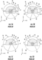
- FIGS. 1A through 1D are cross-sectional views of different examples of prior art polymer clad optical fibers ("fibers") 10.
- Each example fiber 10 includes a central axis AC and has an overall diameter DF.
- Each fiber 10 includes a glass portion defined by a glass core 18 and a glass inner cladding 54.
- the fiber includes an outer cladding 58 positioned around the glass portion 16 and in particular around the glass inner cladding 54.
- the outer cladding 58 is made of a polymer and so is referred to hereinafter as the polymeric outer cladding 58 to distinguish from the glass inner cladding 54.
- the polymeric outer cladding 58 can be composed of two parts: an inner, softer layer and an outer harder layer.
- the polymeric material that makes up the polymeric outer cladding 58 may include high density acrylate, low density acrylate, polyethylene, polystyrene, polymethylmethacrylate, nylon, silicone, silicone based materials, fluorinated acrylates, polyimide, ethylene tetrafluoroethylene, fluoroacrylate, fluoromethacrylate and combinations thereof.
- the polymeric material may be optically transparent.
- the polymeric outer cladding 58 may have a diameter ranging from between about 50 ⁇ m and about 900 ⁇ m, between about 80 ⁇ m and about 250 ⁇ m or between about 100 ⁇ m and 150 ⁇ m.
- the glass inner cladding 54 and the polymeric outer cladding 58 cooperate to form a cladding 22 disposed around the core 18.
- the fiber 10 has an outer surface 24, which in various examples can be defined either by: i) the polymeric outer cladding 58; ii) a portion of the polymeric outer cladding 58 and a portion of the glass inner cladding 54; or iii) a portion of the polymeric outer cladding 58 and a portion of the glass inner cladding 54 and a portion of the core 18; iv) the glass inner cladding 54; (v) a portion of the glass inner cladding 54 and a portion of the core 18.
- the glass portion 16 has a glass-portion surface 62 formed when the fiber 10 is processed to remove some of the glass portion. In an example, this removal process is carried out prior to drawing the fiber 10. Note that in some examples, the glass-portion surface 62 exists only within the glass inner cladding 54 while in other examples the glass-portion surface exists in both the glass inner cladding and the core 18.
- the flat glass-portion surface 62 may be aligned such as generally parallel with the central axis AC of the fiber 10 and/or may extend coaxially with the fiber for either a portion of the fiber 10 or the entire length of the fiber. In an example, the glass core 18 is centered on the central axis.
- the fiber 10 may include one or more stripped portions 28 as shown in FIG. 1D , where a portion, or all of the polymeric outer cladding 58 (e.g., all or part of the cladding 22) along a given length of the fiber has been removed or stripped from the fiber to define the glass-portion surface 62.
- the glass-portion surface 62 is flat, it is referred to as the flat glass-portion surface 62.
- the glass portion 16 includes sides 17 that reside adjacent the glass-portion surface 62. In some cases, for the sake of reference and ease of description, the glass-portion surface 62 can be considered the "bottom" of the glass portion 16.
- the core 18 may be composed of pure silica, doped silica (e.g., doped with germanium, aluminum, titanium, and/or chlorine) and/or other optically transparent materials.
- the glass inner cladding 54 may be composed of pure silica, doped silica (e.g., fluorine, boron, and/or titanium) or other optically transparent materials.
- the fiber 10 may be a single mode fiber or may be a multi-mode fiber.
- the core 18 has a higher refractive index than the glass inner cladding 54.
- the core 18 may have a relative refractive index change, or delta, relative to the glass inner cladding 54 in the range of about 0.2% to about 3.0%, for example about 0.34%, about 0.5%, about 1.0%, about 1.5%, about 2.0%, about 2.5% or about 3.0%.
- the core may also be surrounded by one or more moat or angular rings where the index of refraction is lowered or raised.
- the cladding 22 may be a composite (e.g., glass inner cladding 54 is composed of glass and the polymeric outer cladding 58/polymeric outer cladding 58 is composed of a polymer).
- the refractive indexes of the materials of the cladding 22 generally have a lower refractive index than the core 18. It will be understood that the fiber 10, as described herein, may simply be a connection or connector to another longer or larger optical fiber (not shown).
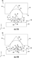
- FIG. 1E is a front-on view that shows the fiber 10 of FIG. 1D operably disposed relative to a photonic device 120 to form an example evanescent coupler 100.
- the photonic device 120 has a support body 121 with a surface 122.
- FIGS. 1F , 1G, and 1H are side views of two example evanescent coupler configurations based on the optical coupler 100 of FIG. 1E .
- the photonic device 120 operably supports within the support body 121 a waveguide core 128 that defines, along with the immediately surrounding portion of the support body, a waveguide 130.
- the waveguide 130 has a surface 132 that resides at or closely proximate to the surface 122.
- the waveguide 130 is planar, i.e., constitutes a planar waveguide.
- the flat glass-portion surface 62 of the fiber 10 is disposed in close, intimate, contact with the surface 132 of the waveguide 130 such that optical signals OS initially carried mainly in the core 18 of the fiber may be transferred to the waveguide or vice versa.
- the fiber 10 extends beyond the left edge of the photonic device 120 and is shown truncated at the left-side edge for ease of illustration.
- the fiber 10 extends beyond the left edge of the photonic device 120 and is shown truncated at the left-side edge for ease of illustration.
- the core 18 of the fiber 10 and the waveguide core 128 reside within a distance DR of each other that allows for an evanescent field of light associated with the optical signals OS propagating through the fiber 10 to enter the waveguide 130, or vice versa.
- the glass-portion surface 62 overlaps the surface 132 of the waveguide 130 in a coupling region 30 by a length LC to facilitate the evanescent coupling.
- the distance DR is called the "coupling distance” while the length LC is called the "coupling length.”
- the fiber 10 bends away from the photonic device 120 to define the coupling region 30.
- the coupling region can also be terminated in FIG. 1F by the photonic device 120 having a right-side edge.
- the coupling region 30 is terminated at the tip (end) 13 of the fiber 10.
- the coupling length LC is the distance over which evanescent coupling occurs between the fiber 10 and the waveguide 130. In an example, the coupling length LC is selected to provide the maximum amount of transfer of energy between the fiber 10 and the waveguide 130. In other examples, the coupling length LC is selected to provide a partial transfer of energy between the fiber 10 and the waveguide 130.
- the optical signals OS are shown initially traveling in fiber 10 and being transferred to the waveguide 130. The optical signals OS can also travel initially in the waveguide 130 and be evanescently coupled into the optical fiber.
- Tapering of the waveguide 130 such that the effective index of the waveguide matches that of the core 18 of the fiber may facilitate or increase the power transfer between the fiber 10 and the waveguide 130. Examples of such tapering are described below.
- the glass portion 16 may take a variety of cross-sectional shapes configured to expose the core surface 26 and/or the cladding surface 62 of the fiber 10 once some of the polymeric outer cladding 58 has been stripped off.
- the cross-sectional shape of the core 18 may be square ( FIG. 1A ), round or circular ( FIG. 1B ), a truncated circle ( FIG. 1C ), or triangular, rectangular, truncated triangular or other polygons configured to define the core surface 26 which extends along a length of the core 18.
- the cross-sectional shape of the core 18 may extend the entire length of the core 18 or may only extend for a portion of the core 18 (e.g., the area intended to be the stripped portion 28 as shown in FIG. 1D ).
- the cross-sectional shape of the core 18 and/or the glass portion 16 may be developed in the preform stage of the fiber 10, and the core 18 and/or the glass portion 16 of the preform may have specific geometries (e.g., corners removed) applied to maintain the core surfaces 26 of the core 18 during production of the fiber 10.
- the core 18 may have a diameter D1 (i.e., the largest straight line dimension or width of the flat core surface 26) of about 6 ⁇ m, about 7 ⁇ m, about 8 ⁇ m, about 9 ⁇ m, about 10 ⁇ m, about 11 ⁇ m, about 12 ⁇ m, about 13 ⁇ m, about 14 ⁇ m or about 50 ⁇ m.
- the core diameter D1 may be large enough such that the mode field diameter of the core 18 is approximately that of a single mode fiber.
- the diameter D1 of the core 18 may also be configured for specific design purposes to have a larger or smaller mode field diameter than standard single mode fiber.
- the diameter of the fiber 10 may be greater than about 50 ⁇ m, greater than about 100 ⁇ m, greater than about 110 ⁇ m, greater than about 120 ⁇ m, greater than about 130 ⁇ m or greater than about 140 ⁇ m. In a specific example, the diameter of the fiber 10 may be about 125 ⁇ m.
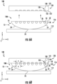
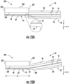
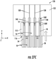
- FIG. 2A is a partially exploded cross-sectional view and FIG. 2B is an assembled cross-sectional view of an example evanescent coupler 100.
- the evanescent coupler 100 includes one or more fibers 10 each having an exposed glass portion 16 at an end section 12 of the fiber.
- the exposed glass portion (hereinafter, simply “glass portion") 16 includes the aforementioned flat glass-portion surface 62 that is aligned to the central axis AC (e.g., runs generally parallel).
- Each fiber 10 also includes an alignment surface 70 that in the example of FIG. 2A is a flat surface that is opposite to and aligned (e.g., generally parallel) to the flat glass-portion surface 62. In some cases, the alignment surface 70 can be considered to reside at the "top" of the glass portion 16.
- the glass-portion surface 62 and the alignment surface 70 can be said to reside on opposite sides of the glass portion 16.
- the alignment surface 70, as well as other alignment features of the fiber 10 discussed below are defined in a fiber preform used to form the fiber.
- the evanescent coupler 100 includes an alignment member 110 that in an example has a planar surface 112 (or alternatively one or more planar sections).
- the alignment member 110 supports the one or more fibers 10 with the alignment surfaces 70 in contact with the planar surface 112.
- the alignment member 100 and the one or more fibers 10 operably supported thereon constitute an alignment assembly 116.
- the evanescent coupler 100 also includes the aforementioned photonic device 120, which can comprise for example a photonic integrated circuit (PIC) or a photonic lightwave circuit (PLC).
- the photonic device 120 operably supports an array of one or more of the waveguide cores 128 within the body 121 of the support body and at or immediately adjacent the surface 122 to define an array of one or more waveguides 130.
- PIC photonic integrated circuit
- PLC photonic lightwave circuit
- each waveguide surface 132 is co-planar with the surface 122 of the support body 121.
- the alignment assembly 116 is disposed relative to the photonic device 120 such that the surface 112 of the alignment member 110 and the surface 122 of the photonic device reside in generally parallel x-y planes. As used herein, generally parallel or parallel means within ⁇ 2 degrees of parallel.
- the alignment assembly 116 and the photonic device 120 are brought together (e.g., by moving the alignment assembly in the z-direction) until the flat glass-portion surfaces 62 of the fibers 10 contact the surface 122 of the photonic device 120, as shown in FIG. 2B .
- the fibers 10 are spaced apart with a period A and the waveguides 130 are also spaced apart with this same period A so that the cores 18 of the fibers align in the x-direction with the cores 128 of the waveguides 130 of the photonic device 120.
- the flat glass-portion surfaces 62 are formed to allow for the respective cores 18 to reside sufficiently close to the corresponding cores 128 of the waveguides 130 (e.g., within the coupling distance DR) to allow for evanescent coupling between the fibers 10 and the waveguides 130.
- the core surface 26 can reside at the glass-portion surface 62 while in another example the core surface 26 can reside within the glass inner cladding 54 in close proximity to the glass-portion surface.
- the flat alignment surfaces 70 of the fibers 10 allows for the flat glass-portion surface 62 and the surface 122 of the photonic device 120 to reside in generally parallel x-y planes so that the fibers and waveguides can be brought into contact without a substantial angular misalignment, i.e., without a substantial relative angular rotation about the y-axis of the two contacting surfaces 62 and 122.
- fiber 10 can be formed with the flat alignment surface 70 and the flat glass-portion surface 62 being generally parallel by machining of the fiber blank used to make the fiber before the blank is drawn into the fiber.
- the two flat surfaces 62 and 70 can be made by extruding a cladding and sleeving the core into it or by soot pressing a cladding of the right shape around a core cane, i.e., cane with the core and a small amount of the cladding.
- the ellipses in FIG. 2A denote that two or more fibers 10 are aligned when the alignment assembly 116 is operably positioned relative to the photonic device 120, as shown in FIG. 2B .
- the surface 112 of the alignment member 110 is flat to less than approximately one micron over the area occupied by the fibers 10.
- the alignment member 110 comprises a rigid material such as glass.
- the surface 112 of the alignment member 110 comprises a compliant material, such as a polymer film, which allows for some small rotational movement of the fibers 10 as they are being pressed into the waveguides 130. Allowance of a small rotational movement allows for a slight adjustment in the position of each fiber 10 if there is slight misalignment when interfacing the alignment assembly 116 with the photonic device 120 (e.g., the surface 112 of the alignment member is not perfectly parallel with the surface 122 of the photonic device).
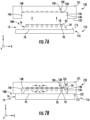
- FIG. 3A is a partially exploded cross-sectional view and FIG. 3B is an assembled cross-sectional view of an example evanescent coupler 100 wherein the photonic device 120 includes alignment channels 140 formed in the surface 122 of the support body and 121, wherein the alignment channels serve as example alignment features.
- the alignment channels 140 run in the y-direction and each includes opposing sidewalls 146 and a bottom surface 148.
- the alignment channels 140 are sized to closely accommodate respective fibers 10 supported on the alignment member 110 of the alignment assembly 116 so that the cores 18 of the fibers align with respective cores 128 of the waveguides 130 of the photonic device 120.
- the cores 128 are centered within the alignment channels 140, i.e., midway between the sidewalls 146.
- the outer surface 24 of the fiber 10 can include angled flat side surfaces 74 on the sides 17 that give the fiber a tapered cross-sectional shape.
- the taper is narrowest at the flat glass-surface portion 62.
- This tapered cross-sectional shape facilitates inserting the fibers 10 into the respective alignment channels 140 to form the assembled evanescent coupler 100, as shown in FIG. 3B.
- FIG. 3B shows by way of example the entire glass portion 16 of each fiber 10 residing within the corresponding alignment channel 140.
- each glass portion 16 can reside partially within its alignment channel 140.
- the glass portions 16 can be said to reside at least partially within its corresponding alignment channel 140.
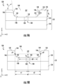
- FIG. 4A is similar to FIG. 3A and shows an example wherein the alignment surface 70 is replaced with or is modified to include an alignment feature in the form of a groove 75 that runs in the y-direction.
- the groove has outside corners 76.
- the surface 112 of the alignment member 110 is modified to include a protrusion 115.
- the protrusion 115 is sized to closely fit within the groove 75 of the fiber 10.
- the protrusion 115 can either be a localized bump or a ridge that runs in the y-direction.
- multiple protrusions 115 can be formed along the y-direction rather than having a single ridge, where the additional protrusions help align and stabilize the fiber by their contact with fiber side surfaces or ridges 77.
- FIG. 4B is a close-up cross-sectional view of a portion of the alignment assembly of FIG. 4A showing the example fiber 10 and a portion of the alignment member 110 that includes the protrusion 115 as received by the groove 75.
- the groove 75 can be used to define two side ridges 77 that can contact the surface 112 of the alignment member 110.
- the outside corners 76 of the groove 75 can contact the surface 112 of the alignment member 110.
- FIG. 4C shows the assembled evanescent coupler 100 formed by operably engaging (interfacing) the alignment assembly 116 and the photonic device 120 of FIG. 4A .
- An advantage of providing alignment features in the form of the groove 75 and the protrusion 115 is that they can provide either point contact or line contact between the fiber 10 and the alignment member 110. Such point contact or line contact makes the evanescent coupler 110 less susceptible to particulate contamination between two flat surfaces, which can cause the fibers 10 to not fully seat on the surface 112 of the alignment member 100. Improper seating can result in a rotational or translational misalignment between the fiber 10 and the waveguide 130.
- the groove 75 can be machined into a fiber blank before draw so that when the fiber is drawn from the blank, the groove 75 will run the length of the fiber.
- the protrusion 115 can be formed on the alignment member 110 with high precision using a laser, especially in the case where the alignment member is made of glass that is amenable to laser-bump formation, such as described for example in U.S. Patent No. 9,359,252 .
- the protrusion 115 can be omitted from the surface 112 of the alignment member 110 so that the two side ridges 77 defined by the groove 75 can rest directly on the surface 112 of the alignment member 110.
- the outside corners 76 defined by the groove 75 can provide lines of contact on the surface 112 of the alignment member 110 of the alignment assembly 116.
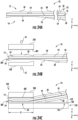
- FIG. 5A is a cross-sectional view of an example multicore fiber 10M that includes multiple cores 18 that reside within a single glass inner cladding 54.
- the single inner cladding is surrounded by a single polymeric outer cladding 58 to define the multipart cladding 22.
- the polymeric outer cladding could also consist of two cladding layers.
- the glass portion 16 comprises the multiple cores 18 and the glass inner cladding 54.
- the cross-sectional shape of the multicore fiber 10M is shown by way of example as rectangular with a height HM and a width WM.
- the cores 18 all reside in a common x-y plane at or immediately adjacent the flat glass-portion surface 62 and have a period ⁇ .
- Example multicore fibers suitable for use in the alignment assembly 116 are disclosed in U.S Patent No. 9,120,693 .
- FIG 5B is a partially exploded side view of an example of the evanescent coupler 100 that shows an example configuration of the alignment assembly 116 wherein the single fibers 10 are replaced by the multicore fiber 10M of FIG. 5A .
- the multicore fiber 10M includes the flat alignment surface 70, which is generally parallel to the flat glass-portion surface 62 and is supported on the top surface 112 of the alignment member 110. Note that the flat glass-portion surface 62 has been formed by processing (e.g., laser processing) the multicore fiber 10M to remove the outer cladding 58 at an end section 12 of the multicore fiber so that only the glass portion 16 remains, with the cores 18 located at or closely proximate to the flat glass-portion surface 62.
- processing e.g., laser processing
- FIG. 5C shows the alignment assembly 116 operably arranged (interfaced) relative to the photonic device 120 to form the evanescent coupler 100, with the cores 18 aligned in the x-direction with corresponding cores 128 of the waveguides 130 of the photonic device, which also have a period ⁇ .
- the respective fiber and waveguide cores 18 and 128 reside sufficiently close to one another (i.e., within the coupling distance DR) to allow for evanescent coupling between the corresponding fibers 10 and the waveguides 130.
- flat glass-portion surface 62 and the flat alignment surface 70 being generally parallel allows for the flat glass-portion surface 62 and the surface 122 of the photonic device 120 to both reside in generally parallel x-y planes and to be brought into contact without a substantial angular misalignment, i.e., without a substantial relative angular rotation about the y-axis of the two contacting surfaces.
- FIGS. 6A and 6B are similar to FIGS. 5B and 5C , respectively, and illustrate an embodiment where the multicore fiber 10M has a non-rectangular cross-sectional shape, with the flat alignment surface 70 being smaller than the flat glass-portion surface 62, and with the remaining portion of the outer surface 24 of the glass section 16 being curved.
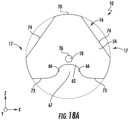
- FIG. 7A and 7B are similar to FIGS. 5B and 5C and illustrate an embodiment similar to that shown in FIGS. 3A and 3B in that the photonic device 120 includes the alignment channel 140.
- the multicore fiber 10M is provided with a tapered cross-sectional shape that is narrowest at the flat glass-portion surface 62. As with the single-fiber embodiment of FIGS. 3A and 3B , the tapered cross-sectional shape of the multicore fiber 10M facilitates inserting the multicore fiber into the alignment channel 140.
- the cores 128 of the waveguides 130 are disposed at or immediately proximate to the bottom 148 of the channel, and the cores 18 of the multicore fiber 10M are brought into alignment with the cores 128 of the waveguides 130, to form the assembled evanescent coupler 100, as shown in FIG. 7B .
- the cores 18 of the multicore fiber 10M need to be placed to with submicron accuracy with respect to the cores 128 of the waveguides 130 to obtain efficient evanescent coupling. Consequently, the flat glass-portion surface 62 and the alignment surface 70 need to be flat to this same sub-micron tolerance.
- the multicore fiber 10M has a form factor (i.e., width to height ratio WM:HM) of 5:1 or less (i.e., WM ⁇ 5HM), and preferably less than 2:1.
- a form factor i.e., width to height ratio WM:HM
- An example of such a multicore fiber 10M has eight cores 18 on a 125 micron pitch A with WM ⁇ HM dimensions of 1.125 mm ⁇ 1.125 mm (i.e., a square or 1:1 form factor) drawn. The dimensions are too large to be wound on a fiber spool.
- the height of the fiber can be reduced for example to 225 microns to allow the fiber to be wound on a fiber spool along the short dimension.
- multicore fiber 10M has eight cores 18 on a 25 micron pitch A with WM ⁇ HM dimensions of 0.225 mm ⁇ 0.225 mm (i.e., a square or 1: 1 form factor) drawn and wound using a conventional fiber draw process.
- a modified draw furnace with axially symmetric heating on both sides of the multicore fiber can be used for fabricating multicore fibers 10M with a greater width-to-height ratio.
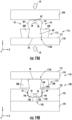
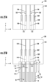
- FIG. 8A is a cross-sectional view of an example photonic device 120 that shows more detail than the photonic devices described above.
- the support body 121 comprises a support substrate 123, an underclad layer 124 disposed atop the support substrate, and an overclad layer 125 disposed atop the underclad layer.
- the waveguide core 128 resides within the overclad layer 125.
- the overclad layer 125 defines the surface 122 of the support body 121.
- An air space 127 is shown adjacent the surface 122.
- the overclad layer 125 includes an alignment channel 140, with the core 128 residing within the channel at or immediately proximate to the bottom 148 of the channel.
- the channel 140 has a width wC and a depth dC.
- the waveguide 130 is defined by the core 128, the underclad layer 124, the overclad layer 125 and the air space 127 adjacent the channel bottom 128.
- the alignment channel 140 can be formed by selectively etching the overclad layer 125.
- the core 128 can be defined by etching a slot in the bottom 148 of the alignment channel 140 and then filling the slot with a relatively high index material as compared to the underclad layer 124 and overclad layer 125.
- the underclad layer 124, the overclad layer 125 and the core 128 are all made of different dielectric materials.
- FIG. 8B is a cross-sectional view of another example photonic device 120 wherein the support body 121 is defined by a unitary support substrate 123 that supports non-optical spacers 126 that define the alignment channel 140.
- the core 128 can be formed in the unitary support substrate 123 by an ion-exchange process into its surface and then the non-optical spacers 126 added to the unitary support substrate.
- the non-optical spacers 126 can be formed using an etch process on either a photoresist layer or a metal layer.
- the etch process that defines the alignment channel 140 can be performed with an alignment accuracy relative to the position of the core 128 of less than 0.5 microns.
- the example photonic devices 120 of FIGS. 8A and 8B show the alignment channel 140 having vertical sidewalls 146.
- the sidewalls 146 need not be vertical and can include other features that facilitate the positioning and alignment of a fiber 10 within the alignment channel 140 so that the fiber core 18 is optimally aligned with the waveguide core 128 of the waveguide 130 of the photonic device 120.
- FIGS. 9A and 9B are similar to FIG. 8A and illustrate an example configuration of the photonic device 120 and in particular the alignment channel 140.
- the sidewalls 146 of the alignment channel 140 can have an angle ⁇ s ⁇ 90° relative to the surface 122 of the photonic device 120.
- the alignment channel 140 can have inside corners 142 that are rounded, e.g., with a radius of curvature in the range from 0.5 micron to 2.0 micron, depending on the etch process conditions.
- the bottom 148 of the alignment channel 140 can be made flat over a reduced width wB (wB ⁇ wC) centered on the waveguide core 128.
- the alignment channel 140 can have rounded outside corners 144 and the sidewalls 146 can be made flat over a select length LS.
- FIG. 9B also shows an example where the alignment channel 140 has two sidewall contact points p1 and p2 that serve as suitable alignment datum locations formed at a known vertical offset y p from the channel bottom 148.
- the sidewall contact points p1 and p2 can be positioned relative to the waveguide core 128 (e.g., at distances x1 and x2 as shown) using precision photolithographic processes.
- x1 x2.
- FIG. 10 shows a fiber 10 having a tapered cross-sectional shape with angled flat surfaces 74 (see also FIG. 3A ) being inserted into the alignment channel 140 of the example photonic device 120 of FIG. 9A .
- the rounded outer corners 144 of the alignment channel 140 help prevent the angled flat surface 74 of the fiber 10 from touching the outer corners as the fiber is inserted into the alignment channel.
- the angled flat surfaces make contact with the rounded outer corners 144 at contact points p1 and p2.
- FIGS. 11A through 11C are schematic close-up views of the fiber core 18 and the waveguide core 128 that show different coupling distances DR for the evanescent coupler 100. Some of the other components of the evanescent coupler 100 are omitted from FIGS. 11A through 11C for clarity.
- the thickness variation in the overclad layer 125 can translate directly to a variation in the coupling distance DR between the waveguide core 128 and the bottom 148 of the alignment channel 140 in the coupling region 30.
- FIG. 11A assumes that the core 18 of fiber 10 is located at the flat glass-portion surface 62 and thus at the bottom 148 of the alignment channel 140.
- FIG. 11B shows an example where the core 18 of the fiber 10 is located in close proximity to the flat glass-portion surface 62. In this case, the waveguide core 128 needs to reside closer to the bottom 148 of the alignment channel 140 so that it is within the coupling distance DR from the core 18 of the fiber 10.
- FIG. 11C shows an example configuration wherein the core surface 26 of core 18 of the fiber 10 is flat and resides at the flat glass-portion surface 62 while the surface 132 of the waveguide resides at the bottom 148 of the alignment channel. In this case, the coupling distance DR ⁇ 0, so that there is greater tolerance for variations in the thickness of the overclad layer 125.
- FIG. 12A is similar to FIG. 10 and shows an example wherein the glass portion 16 of the fiber 10 defines the tapered cross-sectional shape for the fiber and also defines the outer surface 24 of the fiber for an end section 12 of the fiber.
- the tapered cross-sectional shape of the glass portion 16 includes two profile points pp1 and pp2 that define a maximum width WG of the glass portion.
- the tapered cross-sectional shape of the fiber 10 as defined by the glass cladding 16 is formed so that the two profile points pp1 and pp2 contact the contact points p1 and p2 of the sidewalls 146 of the alignment channel 140.
- the widest part of the glass portion 16 resides below the surface 122 of the photonic device 120 and the glass portion does contact the rounded outer corners 144 of the alignment channel 140.
- Precise lateral alignment of the core 18 of the fiber 10 to the core 128 of the waveguide 130 can be achieved by controlling the width wC of the alignment channel 140 so that it substantially matches the maximum width wG of the glass portion 16.
- the widths wC and wG can be in the range from about 10 ⁇ m to 40 ⁇ m and can be controlled to about 0.5 ⁇ m.
- FIG. 12B is similar to FIG. 12A and illustrates an example configuration wherein the polymeric outer cladding 58 of the cladding 22 is configured (e.g., by laser ablation) to also have a tapered configuration.
- the tapered polymeric outer cladding 58 is substantially larger than the tapered glass portion 16 and is used to provide coarse alignment of the glass portion 16 with the alignment channel 140 of the photonic device 120.
- the coarse alignment utilizes a guide layer 200 formed on the surface 122 as defined by the overclad layer 125.
- the guide layer 200 includes a guide slot 210 centered on the alignment channel 140 of the overclad layer 125.
- the guide slot 210 has a width wS that is smaller than the maximum width wT of the tapered polymeric outer cladding 58 (e.g., 70-90% of the width wT), where it serves as a guide feature for placing the fiber 10 in coarse alignment with the alignment channel 140.
- the position of the guide slot 210 does not need to be controlled very precisely to provide suitable coarse alignment of the fiber 10 with the photonic device 120.
- the guide slot 210 can be centered to within 5 ⁇ m to 15 um of the center of the alignment channel 140 and still provide an adequate degree of course alignment.
- FIG. 12C is similar to FIG. 12B and shows an example wherein the polymeric outer cladding 58 of cladding 22 is formed (e.g., via laser ablation) to have a semi-circular cross-sectional shape while the glass portion 16 has a rounded rectangular cross-sectional shape that substantially matches the size and shape of the alignment channel 140.
- the glass portion 16 includes the flat glass-portion surface 62 at which the core 18 resides.
- the polymeric outer cladding 58 has a bottom surface 21 that confronts the surface 122 of the photonic device 120 when the glass cladding 16 is operably positioned in the alignment channel 140.
- FIG. 13A is similar to FIG. 12A and illustrates an example wherein the fiber 10 has a glass portion 16 with cross-sectional shape similar to that shown in FIG. 1B .
- the polymeric outer cladding 58 has been removed (e.g., via laser ablation) from the end section 12 to define the flat glass-portion surface 62 of the glass portion 16.
- the glass portion 16 of the fiber 10 of FIG. 13A has rounded outer corners 63 each having a radius of curvature the same as or less than that of the rounded inside corners 142 of the alignment channel 140. This allows for the glass portion 16 to reside within the alignment channel 140 with the flat glass-portion surface 62 in contact with the bottom 148.
- the (maximum) width wG of the glass portion 16 is substantially equal to the width wC of the alignment channel 140 so that the profile points pp1 and pp2 of the glass portion contact the contact points p1 and p2 of the sidewalls 146, noting that some space is shown between the glass portion and sidewalls for ease of illustration.
- FIG. 13B is similar to FIG. 13A and illustrates an example wherein the otherwise flat glass-portion surface 62 includes a central section 61 wherein the core 18 resides within the coupling distance DR.
- the central section 61 can also be referred to as the coupling section since the evanescent coupling occurs through this part of the glass-portion surface 62. In an example, this is accomplished by the central section 61 having a central ridge 65C aligned with the core 18.
- the central ridge 65C can be formed by selectively laser ablating the flat glass-portion surface 62 so that the core 18 resides partially within the central ridge.
- the central ridge 65C is used to ensure that the glass portion 16 at which the core 18 resides contacts the bottom 148 of the alignment channel 140 at which the waveguide core 128 resides.
- the central ridge 65C can be also serve to provide a more concentrated force between the glass portion 16 and the bottom 148 of the alignment channel 140. The more concentrated force can ensure close contact, especially in the presence of debris, which can form an unwanted gap (or increase the size of the desired coupling distance DR) between the fiber core 18 and the waveguide core 128 in the coupling region 30. Note that the central ridge 65C remains in contact with the bottom 148 of the alignment channel 140 even if the glass portion 16 rotates about the fiber central axis AC within the alignment channel.
- FIG. 13C is similar to FIG. 13B and shows an example where the flat glass-portion surface 62 is further processed to have two outboard or "side" bumps 65S in addition to the central ridge 65C.
- the side ridges 65S are formed to provide additional precision contact points p3 and p4 for alignment of the core 18 of the fiber 10 to the core 128 of the waveguide 130 when the fiber 10 is operably disposed in the alignment channel 140.
- the side ridges 65S can allow for the fiber 10 to rotate slightly upon insertion into the alignment channel 140 so that the fiber core 18 is always precisely aligned to waveguide core 128.
- the side ridges 65S and the central ridge 65C define two longitudinal gaps GD between the flat glass-portion surface 62 of the glass portion 16 and the bottom 148 of the alignment channel 140.
- the gaps GD provide a place for debris to migrate during the insertion of the fiber 10 into the alignment channel 140.
- FIG. 13D is similar to FIGS. 13B and 13C and illustrates an embodiment wherein the glass-portion surface 62 of the glass portion 16 is rounded rather than flat.
- This configuration for the glass portion 16 may be easier to fabricate than the configuration that has the central ridge 65C while still providing gaps DG for debris collection.
- This rounded configuration tolerates modest fiber rotational misalignment about the fiber central axis AC without significantly changing the coupling distance DR.
- FIG. 13D also shows an example where alignment member 110 of the alignment assembly 116 includes an alignment feature 115 in the form of a V-groove 115V formed in the surface 112 of the alignment member 110.
- the V-groove 115V makes contact with a now curved alignment surface 70 of the glass portion 16 at two contact points p5 and p6.
- Use of the alignment member 110 in the alignment assembly 116 allows for a looser fit of the glass portion 16 within the alignment channel 140.
- FIG. 13E is similar to FIG. 13A and illustrates an embodiment where the glass portion 16 includes the flat glass-portion surface 62 and the flat alignment surface 70 generally parallel to the flat glass-portion surface, similar also to the embodiment of fiber 10 of FIG. 10 described above. Having generally parallel surfaces 62 and 70 makes the cladding profile more symmetric so that it can be more readily formed without distortion during the drawing process. Making the sides 17 of the glass portion 16 that reside adjacent the sidewalls 146 of the alignment channel 140 symmetrical about the z-axis axis can further improve the ability to maintain the desired cladding profile of the fiber 10 during the drawing process, as well as providing for symmetric contact points p1 and p2 on sidewalls 146 of the channel 140.
- FIG. 14A shows an example alignment member 110 initially positioned above the flat alignment surface 70 of the glass portion 16 of an example fiber 10 as a first step in fabricating an example evanescent coupler 100.
- an alignment jig 320 having a top surface 322 in which an alignment groove 324 is formed.
- the alignment groove 324 has a bottom 326.
- the glass portion 16 is shown supported in the alignment groove 324, with the core 18 located closest to the bottom 326 of the alignment groove.
- the alignment jig 320 can include multiple alignment grooves 324 having the same period A as the alignment channels 140 of the photonic device 120.
- the alignment member 110 includes a support sheet 302, an elastomeric layer 304 supported by the support sheet, and an adhesive layer 306 supported by the elastomeric layer.
- the adhesive layer defines the surface 112 of the alignment member 110.
- the alignment member 110 is disposed with the adhesive layer 306 confronting the flat alignment surface 70 of the glass portion 16.
- FIG. 14B shows the next step in the fabrication process, wherein the alignment member 110 is brought into contact with the glass portion 16 so that the flat alignment surface 70 of the glass portion bonds to the adhesive layer 306.
- the alignment jig 320 is then removed, leaving the structure shown in FIG. 14C , which forms an alignment assembly 116.
- the alignment member 110 and the glass portion 16 bonded thereto is used to deploy the glass portion 16 into the alignment channel 140 of the photonic device 120 to form the final evanescent coupler 100.
- the elastomeric layer 304 is optional and used to allow the glass portion 16 to be deflected slightly during the deployment process.
- the fabrication process can be applied to an array of fibers 10 to ensure that the glass portions 16 of the fibers are positioned in respective alignment channels 140 of the photonic device 120 with a precise center-to-center pitch (i.e., period) A.
- FIG. 15A is a cross-sectional view that shows a first step in an example assembly process for forming an example evanescent coupler 100.
- the alignment surface 70 of the glass portion 16 of the fiber 10 has a V-shape profile while the alignment member 110 is similar to that of FIG. 13D and includes the V-shaped alignment groove 115V complementary to the V-shape alignment surface.
- the alignment member 110 can include multiple spaced-apart V-shaped alignment grooves 115V having a select period ⁇ .
- the V-shaped alignment surface 70 of the glass portion 16 is urged into the V-shaped alignment groove 115V using a pressing member 350, which in an example can comprise the another alignment member 110 as described above but without the adhesive layer 306 so that the elastomeric layer 304 contacts the flat glass-portion surface 62 of the glass portion 16.
- the optional elastomeric material 304 of the pressing member 350 helps prevent damage to the flat glass-portion surface 62 of the glass portion 16 that could occur if a hard material (e.g., a glass sheet) is used.
- the elastomeric material 304 also allows the V-shaped alignment surface 70 of the glass portion 16 to rotate slightly about the central axis AC of the fiber 10 as it is forced into the V-shaped alignment groove 115V.
- An adhesive material 307 is used to bond the V-shaped alignment surface 70 of the glass portion 16 within the V-shaped alignment groove 115V of the alignment member 110.
- the application of the adhesive material 307 is controlled to prevent excess adhesive material from reaching the flat glass-portion surface 62 of the glass portion 16.
- at least one thin layer of the adhesive material 307 may be applied to the top surface 112 of the alignment member 110 and in the V-shaped alignment groove 115V prior to inserting the V-shaped alignment surface 70 into the alignment channel.
- the adhesive material 307 may be applied using a spin-on technique.
- the alignment member 110 can be configured with multiple V-shaped grooves 115V to support an array of fibers 10 having the select period ⁇ .
- FIG. 15C shows the next step in the fabrication process, wherein the alignment assembly 116 is inverted and aligned with the alignment channel 140 of the photonic device 120.
- the alignment assembly 116 and the photonic device 120 are then brought together (interfaced) so that the part of the glass portion 16 that includes the flat glass-portion surface 62 resides within the alignment channel 140, with the flat glass-portion surface in contact with or in close proximity to the bottom 148 of the alignment channel, thereby forming the evanescent coupler 100.
- the core 18 of the fiber 10 resides sufficiently close to the core 128 of the waveguide 130 (e.g., within the coupling distance DR) to enable evanescent coupling as described above.
- FIG. 15D is similar to FIG. 15C and illustrates an example wherein the alignment surface 70 of the glass portion 16 has a modified V-shape that provides for multiple contact points p5, p6 and p7 between the glass portion and the V-shaped alignment groove 115V of the alignment member 110, in addition to the aforementioned contact points p1 and p2 between the glass portion and the channel sidewalls 146.
- This can be accomplished for example by introducing a slight curvature to the otherwise flat surfaces that define the general V-shape of the alignment surface 70.
- FIG. 15E is similar to FIG. 15D and shows an example configuration of the evanescent coupler 100 wherein the alignment surface 70 of the glass portion 16 has a rounded V-shape that provides two contact points p5 and p6 with the V-shaped alignment groove 115V of the alignment member 110.
- the glass portion 16 can be rotated within the V-shaped alignment groove 115V so that the flat glass-portion surface 62 of the glass portion 16 is generally parallel with the top surface 112 of the alignment member 110. This ensures that if the top surface 112 of the alignment member 110 is generally parallel with the top surface 122 of the photonic device 120, the glass portion 16 will be properly seated within the alignment channel 140 of the photonic device for evanescent coupling.
- Fibers 10 used in evanescent coupling to planar waveguides 130 of a photonic device 120 can extend to remote locations where optical connectors are required.
- Most commercially available optical connector ferrules e.g., MTP, LC, and SC connector ferrules
- MTP, LC, and SC connector ferrules are designed to accept fibers that have a standard outside diameter (e.g. 125 ⁇ m for SMF-28 fiber). It may therefore be desirable for the fiber 10 to have a cladding 22 configured for dual use, i.e., for use at one end in evanescent coupling configurations of the evanescent couplers 100 as well as for use at its other end with standard optical connector ferrules.
- FIG. 16A is a cross-sectional view of an example fiber 10 residing within an interior 372 of a ferrule 370.
- the glass portion 16 of the fiber 10, which includes the core 18 and glass inner cladding 54, has a D-shape (i.e., semi-circular shape) with a diameter D2, which in an example is 125 ⁇ m.
- a dashed circle is used to show the perimeter of the glass portion 16 for clarity.
- the core 18 of the fiber 10 is located at or in close proximity to the flat glass-portion surface 62 as well as centered on the central axis AC so that it can be coaxially aligned with a standard SMF-28 optical fiber within the ferrule 370.
- FIG. 16B shows a modified profile for the glass portion 16 of cladding 22 of the fiber 10, wherein the glass-portion surface 62 is shaped such that 75% or greater of the glass portion 16 is curved with the diameter D2.
- the glass portion 16 fills substantially greater than 50% of the interior 372 of the ferrule 370. This in turn greatly reduces the amount of vertical play when the glass portion 16 is held within the standard ferrule 370.
- the profile of the glass portion 16 of FIG. 16B includes a groove 67 in the central section 61 of the glass-portion surface 62 so that the core 18 of the fiber 10 resides at or closely proximate to flat glass-portion surface 62 for evanescent coupling to exterior waveguides 130, which in an example can be another optical fiber.
- the groove 67 can be designed to serve as an alignment feature for aligning to an exterior waveguide 130.
- FIG. 17A shows an example alignment assembly 116 with the glass portion 16 of fiber 10 of FIG. 16B held within the V-shaped alignment groove 115V of the alignment member 110.
- the alignment assembly 116 is shown in position relative to an example photonic device 120 in anticipation of interfacing the alignment assembly to the photonic device to form an evanescent coupler 100.
- the waveguide 130 resides atop the underclad layer 124 and has the form of a ridge waveguide.
- the overclad layer 125 surrounds the core 128 on three sides and is processed (e.g., etched) so that the ridge waveguide 130 has a select width wR and a select height hR so that the cross-sectional shape of the ridge waveguide is substantially complementary to the cross-sectional shape of the groove 67 formed in the glass portion of the fiber 10.
- FIG. 17B shows the assembled evanescent coupler 100 with the ridge waveguide 130 residing within the groove 67 of the glass portion 16 so that the core 18 of the fiber is sufficiently close to the core 128 of the ridge waveguide (e.g., within the coupling distance DR) for evanescent coupling.
- the groove 67 can have tapered sidewalls 66 (see FIG. 17A ) that facilitate guiding the ridge waveguide 130 into the groove.
- External alignment aids (not shown) can also be employed when operably interfacing the alignment assembly 116 with the photonic device 120.
- the groove 67 in the glass portion 16 defines two bumps 73 at the glass-portion surface 62.
- the bumps 73 may be designed to either contact the surface 122 of the photonic device 120 or to reside just above the surface to ensure that the ridge waveguide 130 is properly situated within the groove 67 for evanescent coupling to occur between the fiber 10 and the ridge waveguide.
- FIG. 18A is a cross-sectional view of an example fiber 10 wherein the glass portion 16 of the cladding 22 has a profile similar to that of FIG. 16B , except that the round portion of the outer surface 24 at the sides 17 now includes two flat angled sections 74 (see also FIGS. 3A and 3B ) that give the glass portion 16 a generally triangular or V shape.
- FIGS. 18B and 18C are similar to FIGS. 17A and 17B and show the glass portion 16 of the cladding 22 of the fiber 10 of FIG. 18A held by the alignment member 110 to form an example alignment assembly 116.
- the flat sections 80 of the glass portion 16 are configured so that the glass portion closely fits within the V-shaped alignment grooves 115V of the alignment member 110.
- FIG. 19A shows an example fiber 10 wherein the glass portion 16 has a keyhole cross-sectional shape with a dovetail section 82 that includes the alignment surface 70 and a bulbous section 84 that includes the glass-portion surface 62.
- the alignment assembly 116 is formed by inserting the dovetail section 82 into an alignment feature 115 in the form of an alignment channel 115D that has a complementary cross-sectional shape to the dovetail section.
- the alignment channel 115D is defined by two generally parallel-running flexible gripping elements 328 supported on the surface 112 of the alignment member.
- a pressing member 350 e.g., a glass sheet or glass member is used to press against the flat glass-portion surface 62 to push the glass portion 16 into the alignment channel 115D to form the example alignment assembly 116.
- the flexible gripping elements 328 simultaneously center the glass portion 16 and hold it down in contact with the alignment member 110.
- the flexible gripping elements 328 can be made of a polymer or other elastomeric material.
- the alignment assembly 116 of FIG. 19A can be inverted and then operably interfaced with a photonic device 120 to form an example evanescent coupler 100, shown in FIG. 19B .
- the bulbous section 82 of the glass portion 16 is shown contacting the sidewalls 146 of the alignment channel 140 at the two contact points p1 and p2 while the flat glass-portion surface 62 is in contact with the bottom 148 of the alignment channel 140. This aligns the core 18 of the fiber 10 with the core 128 of the waveguide 130 of the photonic device 120.
- the keyhole-shaped glass portion 16 is free to defect laterally (left-right) while inserting the glass portion into the alignment channel 140.
- the keyhole shaped profile of the glass portion 16 of the fiber 10 forms a tongue-and-groove type of joint with the polymeric outer cladding 58 of the cladding 22 that serves to keep these two cladding portions together for the part of the fiber 10 outside of the coupling region 30 where the inner and outer claddings 54 and 58 remain intact to define cladding 22.
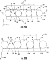
- FIG. 20A is similar to FIG. 19A and illustrates an example alignment assembly 116 that supports multiple fibers 10 each having a glass portion 16 with the keyhole cross-sectional shape described above.
- the alignment assembly 116 includes multiple spaced-apart (e.g., interdigitated) optical fibers 400 supported on surface 112 of the alignment member 110 and that serve as spacers that define spaced apart alignment channels 115D having the select period ⁇ .
- the optical fibers 400 are thus referred to hereinafter as "optical-fiber spacers.”
- the dovetail sections 82 of the glass portions 16 of the fibers 10 reside within the alignment channels 115D, with the flat alignment surfaces 70 in contact with the surface 112 of the alignment member 110, while the flat glass-portion surface 62 face upward.
- An adhesive material 307 can be used to secure the optical fiber spacers 400, the support substrate 110 and the dovetail sections 82 of the glass portions 16 to one another.
- Squeezing forces FS can be applied in the horizontal and vertical directions while the adhesive material 307 cures (e.g., via UV radiation).
- a temporary pressing member 350 such as a glass sheet, can be employed at the flat glass-portion surfaces 62 to facilitate the even application of the vertical squeezing forces and to set the dovetail sections 82 within the optical fiber spacers 400.
- the temporary pressing member 350 can be removed, exposing the flat glass-portion surfaces 62 of the keyhole-shaped glass portions 16 of the fibers 10 in the alignment assembly 116, as shown in FIG. 20B .
- the alignment assembly 116 can then be flipped over so that the flat glass-portion surfaces 62 face downward. Since the squeeze assembly approach ensures that the glass portions 16 are arranged on the precise period A, the flat glass-portion surfaces 62 can be aligned to the same-period alignment channels 140 of a photonic device 120 in the manner discussed above.
- U.S. Patent Application No. 15/405,396 discusses examples of stripping a portion of the polymer cladding 22 of the fiber 10 (e.g. some or all of the polymeric outer cladding 58) using laser processing. The discussion below is directed to improved methods of forming an alignment assembly 116 using such laser processing.
- FIG. 21A is a partially exploded top-elevated view of an example array of fibers 10 each having an end section 12 where the polymeric outer cladding 58 of the cladding 22 is stripped away to reveal the glass portion 16.
- a shaping member 330 is shown disposed below the glass portions 16 of the fibers 10.
- the shaping member 330 has a top 332, a bottom 334, a front end 335 and a back end 337.
- the shaping member 330 can be formed from a drawn glass sheet having a desired cross-sectional shape and that is cut to the desired size.
- the shaping member 330 can also be formed using one or more other processes alone or in combination, such as a fusion draw process, a redraw process, a hot pressing process and a flame working process.
- FIGS. 21B and 21C are top and bottom elevated views of the resulting alignment assembly 116, with the glass portions 16 bonded to the bottom 335 of the shaping member 330 using an adhesive material 307.
- FIGS. 22A and 22B are side views of the alignment assembly 116 shown in FIGS. 21B and 21C .
- the end sections 12 of the fibers 10 need to be shaped so that the flat glass-portion surface 62 of the glass portion 16 can be used to establish contact with the corresponding waveguides 130 of a photonic device 120 for evanescent coupling. In some cases such as shown in FIGS. 22A and 22B , the shaping extends beyond the portion of the fiber 10 that constitutes the coupling region 30. Note that in FIGS. 22A and 22B , the end section 12 of the glass portion includes a thin portion of the glass inner cladding 54, as shown in the close-up inset of FIG. 22A .
- the shaping of the end sections 12 of fibers 10 can be achieved by removing (e.g., via laser ablation) select parts of the polymeric outer cladding 58 of the cladding 22 that resides adjacent the back end 337 of the shaping member 330, as shown by the dashed line in FIG. 22A .
- This allows for the fiber 10 to be bent as shown in FIG. 22B so that the flat glass-portion surface 62 can reside in the x-y plane over the coupling length LC to define the coupling region 30.
- the bending process also defines a flat cladding section 22F that resides immediately adjacent and in the same plane as flat-glass portion 62 associated with the coupling region 30.
- FIG. 23A is an elevated view of an example shaping member 330 that has a curved bottom 334 that gives the shaping member a curved y-z cross-sectional shape.
- the curved bottom 334 is bonded with the glass portions 16 of the fibers 10 so that after bonding, the glass portions 16 conform to the curved bottom of the shaping member 330 to define an axially extending section of the flat glass-portion surface 62 of the glass portion 16 that serves to define the coupling region 30.
- the curved bottom 334 of the shaping member 330 helps minimize local stresses where glass portion 16 is bent.
- the shaping member 330 can be extended in size so that it supports the unstripped fiber 10.
- Application of the adhesive material 307 at and near the bend in the glass portions 16 at the back end 337 of the shaping member 330 can be used to further reduce local bend stresses.
- FIGS. 23B and 23C are similar to FIGS. 22A and 22B but show the use of the curved shaping member 330.
- FIG. 24A is a cross-sectional view of the end section 12 of an example fiber 10 wherein the cladding 22 has been processed using a laser beam to create a select cladding profile amenable for shaping the end section 12 of the fiber.
- FIG. 24B shows the processed cladding 22 of the fiber 10 disposed between the shaping member 330 and a shaping jig 430 as part of a shaping process for the end section 12 of the fiber 10.
- the bottom 334 of the support substrate 330 is flat and includes a layer of adhesive material 307.
- the select cladding profile is such that when a squeezing force FS is applied to the shaping member 330 and the shaping jig 430, the glass portion 16 bends so that the top part of the cladding 22 conforms to the flat bottom 334 of the shaping member 330.
- the layer of adhesive material 307 maintains the conformal shape, allowing for the shaping jig 430 to be removed.
- the layer of adhesive material 307 can comprise a UV-curable adhesive, and the process can include irradiation of the UV-curable adhesive with UV light.
- FIG. 24C The result of the shaping process is shown in FIG. 24C , wherein the end section 12 of the fiber 10 takes on a U-shaped profile.
- An axial section of the flat glass-portion surface 62 has the coupling length LC and defines the coupling region 30 when the fiber 10 is operably arranged relative to the waveguide 130 of the photonic device 120 when forming the evanescent coupler 100.
- each fiber 10 includes adjacent the fiber tip 13 a triangular shaped piece 20T of the polymeric outer cladding 58 of cladding 22.
- This triangular shaped piece 20T of the polymeric outer cladding 58 serves as a bumper after the end sections 12 of the fibers 10 are bonded to the shaping member 330.
- the bumper 20T serves as small elastic feature that can limit the leftward travel of the fibers 10 during alignment with the waveguides 130 of the photonic device 120.
- FIGS. 25A and 25B are similar to FIG. 24C and show an example wherein the front end section 12 of the fiber 10 is processed (e.g., laser processed with a laser beam LB or polished) to form an angled tip 13 at the front end section 12.
- This process can also be used to define or control the coupling length LC of axially extending glass-portion surface 62 that defines the coupling region 30.
- FIG. 26 is a top down view of an example alignment assembly 116 that shows the glass portions 16 of four fibers 10 supported on the top 112 of an example alignment member 110.
- the alignment member 110 is made of a transparent material such as glass.
- the polymeric outer claddings 58 of the claddings 22 of each fiber 10 have been processed as described above so that the axially extending flat glass-portion surface 62 has a desired coupling length LC.
- FIG. 27A is a plan view of an example photonic device 120 having four cores 128 that define planer waveguides 130, wherein the cores are terminated by respective tapered ends 128T that define a tapered waveguide portions 130T of waveguides 130.
- the tapered waveguide portions 130T extend into the alignment channels 140 of the photonic device 120, with the tapered cores 128T residing at or proximate to the bottoms 148 of the alignment channels.
- the tapered waveguide portions 130T define the coupling regions 30 for the resulting evanescent coupler 100 as described below.
- FIG. 27B shows the alignment assembly 116 in position to be interfaced with the photonic device 120.
- the alignment channels 140 have open ends 141 into which the glass portions 16 of the fibers 10 are respectively inserted.
- FIG. 27C shows the alignment assembly 116 in operable position with the photonic device 120 to form the evanescent coupler 100.
- the cores 18 of the fibers 10 are aligned with and in close proximity to the tapered waveguide portions 130T so that evanescent coupling can occur between each fiber and the corresponding tapered waveguide portion of the waveguide 130.
- FIG. 28A is similar to FIG. 27B and shows an example wherein the alignment channels 140 of the photonic device 120 have flared open ends 141 to facilitate inserting the glass portions 16 of the fibers 10 into the corresponding alignment channels by allowing for a degree of lateral misalignment during the initial insertion.
- the lateral misalignment tolerance may be as large as ⁇ 50-100 ⁇ m using the flared ends 141 of the alignment channels 140.
- FIG. 28B shows the glass portions 16 fully inserted into the corresponding alignment channels 140 to form the evanescent coupler 100.
- FIG. 29A is similar to FIG. 27A and illustrates an embodiment wherein the alignment channels 140 include flared open ends 141 and are also made excessively wide (i.e., wider than the glass portion 16 of the fiber 10) and also with the waveguide cores 128 offset from the center of the channels so that only one sidewall 146 of the alignment channel serves as a precision reference (alignment) surface.
- This approach enables different motion paths for the alignment assembly 116 relative to the photonic device 120 when interfacing the alignment with the photonic device to form the evanescent coupler 100.
- a first example of a motion path MP includes a first movement of the alignment assembly 116 in an axial direction that positions the glass portions 16 adjacent the leftmost sidewalls 146 of the alignment channels 140.
- the motion path also includes a second movement of the alignment assembly 116 in the +x (lateral) direction, which forces the glass portions 16 into the opposite sidewalls 146 of the alignment channels 140 to cause alignment of the cores 18 of the fibers 10 with the tapered cores 128T of the tapered waveguide portions 130T of the waveguides 130.
- the configuration may also reduce the likelihood of debris being trapped between the glass portions 16 and the sidewalls 146 of the alignment channels 140 since the motion of the glass portions during the insertion and alignment process provides a sweeping motion that may move debris away from critical reference surfaces prior to contact.
- the axial and lateral motions are combined to define a second example motion path MP with a single angled direction of motion.
- the axial and lateral motions are replaced with curved, J-shaped motion path MP.
- the motion paths MP for the alignment assembly 116 are defined in the plane of the photonic device 120.
- the motion paths can be determined by mechanical features (not shown) of connector elements that hold the alignment assembly 116. These mechanical features can include slot, rail, and cam structures that guide the alignment assembly 116 into position during coarse and fine alignment operations.
- the motion paths MP can have small movement components that are out of the plane of the photonic device 120.
- the term "coupled” in all of its forms: couple, coupling, coupled, etc. generally means the joining of two components (optical, electrical or mechanical) directly or indirectly to one another. Such joining may be stationary in nature or movable in nature. Such joining may be achieved with the two components (optical, electrical or mechanical) and any additional intermediate members being integrally formed as a single unitary body with one another or with the two components. Such joining may be permanent in nature, or may be removable or releasable in nature, unless otherwise stated. It will be apparent to those skilled in the art that various modifications and variations can be made without departing from the scope of the claims.
Landscapes
- Physics & Mathematics (AREA)
- General Physics & Mathematics (AREA)
- Optics & Photonics (AREA)
- Optical Couplings Of Light Guides (AREA)
Claims (13)
- Procédé de mise en oeuvre d'un couplage optique évanescent, comprenant :fournir au moins une fibre optique (10) ayant un axe central (AC), un coeur de verre (18) et un revêtement (54, 58), le revêtement (54, 58) comprenant un revêtement interne (54) fait de verre et un revêtement externe (58) fait d'un polymère, et dans lequel le coeur de verre (18) et le revêtement interne de verre (54) définissent une partie en verre (16) de la fibre ;traiter la au moins une fibre optique (10) pour définir une partie dépouillée (28) sensiblement dépourvue du revêtement externe (58) et configurée pour exposer la partie en verre (16), dans lequel la partie en verre exposée (16) définit : i) une première surface plate parallèle à l'axe central (AC), dans lequel le coeur de verre (18) réside à ou est étroitement proche de la première surface plate ; et ii) une surface comprenant une caractéristique d'alignement (70, 75) ;retirer au moins une partie du revêtement externe (58) adjacent à la partie en verre exposée (16) pour permettre de courber la fibre optique (10) ; etcourber la fibre optique (10) pour définir une longueur de couplage axial (LC) pour la partie en verre exposée (16) ; engager de manière opérationnelle la caractéristique d'alignement (70, 75) avec un membre d'alignement (115) de manière à ce que le membre d'alignement (115) soutienne de manière opérationnelle la partie dépouillée (28) pour définir un ensemble d'alignement (116) ;caractérisé en ce que le procédé comprend en outre l'étape consistant àrapprocher l'ensemble d'alignement (116) et un dispositif photonique (120) de manière à ce que le coeur de verre (18) soit rapproché suffisamment près de et en alignement relatif avec un coeur de guide d'ondes (128) d'au moins un guide d'ondes afin d'établir un couplage évanescent entre la au moins une fibre optique (10) et le au moins un guide d'ondes (130) sur la distance de la longueur de couplage axial.
- Procédé selon la revendication 1, dans lequel la au moins une fibre optique (10) comprend de multiples fibres optiques (10), le au moins un guide d'ondes comprend de multiples guides d'ondes (128) soutenus de manière opérationnelle dans des canaux d'alignement respectifs (140) du dispositif photonique (120), et insérer les parties en verre (16) des multiples fibres optiques dans des canaux respectifs des canaux d'alignement (140).
- Procédé selon la revendication 2, dans lequel insérer les parties en verre (16) des multiples fibres optiques dans des canaux respectifs des canaux d'alignement (140) comprend insérer les parties en verre dans des extrémités ouvertes évasées respectives des canaux d'alignement (140).
- Procédé selon la revendication 3, dans lequel chaque canal d'alignement comprend une première et une deuxième paroi latérale opposées (146) et est plus large que la partie en verre (16), dans lequel les guides d'ondes résident chacun respectivement le plus près de la première paroi latérale, et comprenant en outre :
déplacer l'ensemble d'alignement (116) sur un chemin de déplacement ce qui fait que les parties en verre de chaque fibre optique (10) sont déplacées en une position alignée lorsque entrant en contact avec la première paroi latérale. - Procédé selon l'une quelconque des revendications précédentes, où le procédé comprend retirer une partie du revêtement externe à une section d'extrémité (12) de la fibre (10) pour définir la partie en verre exposée (16).
- Procédé selon l'une quelconque des revendications précédentes, dans lequel ledit fait de retirer comprend un ablation au laser.
- Procédé selon l'une quelconque des revendications précédentes, dans lequel ledit fait de courber la fibre optique comprend presser la partie en verre exposée (16) contre une surface courbée (334) d'un membre de mise en forme (330).
- Procédé selon l'une quelconque des revendications précédentes, dans lequel ledit fait de courber la fibre optique (10) comprend mettre la partie en verre exposée (16) en sandwich entre un membre de mise en forme (330) et un gabarit de mise en forme (430) et appliquer une force de compression au membre de mise en forme (330) et au gabarit de mise en forme (430).
- Procédé selon l'une quelconque des revendications 1-8, comprenant en outre soutenir les multiples parties en verre par rapport à des rainures d'alignement (324) d'un gabarit d'alignement (320), dans lequel les rainures d'alignement (324) ont une même période A que les canaux d'alignement (14) du dispositif photonique (120) ; et
utiliser le gabarit d'alignement (320) pour positionner les multiples parties en verre sur le membre d'alignement (115) de sorte que les multiples parties en verre définissent la période A. - Procédé selon la revendication 9, comprenant en outre recevoir les multiples parties en verre sur une surface résiliente du membre d'alignement (115).
- Procédé selon l'une quelconque des revendications 1-10, dans lequel la partie en verre exposée a un profil en forme de clé avec une partie bulbeuse (84) qui comprend la première surface plate et une partie en queue d'aronde (82) qui comprend la caractéristique d'alignement (70), et comprenant en outre :
gripper la partie en queue d'aronde (82) avec des éléments de grippage soutenus par le membre d'alignement (115). - Procédé selon la revendication 11, dans lequel la au moins une fibre optique comprend de multiples fibres optiques ayant une période A sélectionnée, dans lequel la partie en verre exposée de chaque fibre optique a un profil en forme de clé avec une partie bulbeuse (84) qui comprend la première surface plate et une partie en queue d'aronde (84) qui comprend la caractéristique d'alignement (70), et comprenant en outre :
arranger les parties en verre exposées des multiples fibres optiques (10) sur le substrat d'alignement avec des pièces d'écartement de fibres optiques (400) résidant entre les parties en verre exposées afin de définir des canaux d'alignement espacés ayant la période A sélectionnée. - Procédé selon l'une quelconque des revendications 1-12, comprenant en outre définir la première surface plate et la caractéristique d'alignement dans une préforme utilisée pour dessiner la au moins une fibre optique.
Applications Claiming Priority (2)
| Application Number | Priority Date | Filing Date | Title |
|---|---|---|---|
| US15/884,622 US10514506B2 (en) | 2018-01-31 | 2018-01-31 | Optical couplers for evanescent coupling of polymer clad fibers to optical waveguides using alignment features |
| PCT/US2019/015756 WO2019152455A1 (fr) | 2018-01-31 | 2019-01-30 | Coupleurs optiques destinés au couplage évanescent de fibres revêtues de polymère à des guides d'ondes optiques à l'aide de caractéristiques d'alignement |
Publications (2)
| Publication Number | Publication Date |
|---|---|
| EP3746826A1 EP3746826A1 (fr) | 2020-12-09 |
| EP3746826B1 true EP3746826B1 (fr) | 2023-11-29 |
Family
ID=65409623
Family Applications (1)
| Application Number | Title | Priority Date | Filing Date |
|---|---|---|---|
| EP19705050.3A Active EP3746826B1 (fr) | 2018-01-31 | 2019-01-30 | Coupleurs optiques destinés au couplage évanescent de fibres revêtues de polymère à des guides d'ondes optiques à l'aide de caractéristiques d'alignement |
Country Status (3)
| Country | Link |
|---|---|
| US (1) | US10514506B2 (fr) |
| EP (1) | EP3746826B1 (fr) |
| WO (1) | WO2019152455A1 (fr) |
Families Citing this family (15)
| Publication number | Priority date | Publication date | Assignee | Title |
|---|---|---|---|---|
| US10545290B2 (en) * | 2016-01-18 | 2020-01-28 | Corning Incorporated | Polymer clad fiber for evanescent coupling |
| US10962720B2 (en) * | 2018-07-17 | 2021-03-30 | The Trustees Of Columbia University In The City Of New York | 3D funnel photonic structure for fiber to waveguide coupling |
| US11275213B2 (en) * | 2018-10-31 | 2022-03-15 | Corning Research & Development Corporation | Methods of forming optical fibers having an expanded core for evanescent optical coupling |
| WO2020112645A1 (fr) * | 2018-11-30 | 2020-06-04 | Commscope Technologies Llc | Dispositfs, systèmes et procédés d'alignement de fibres optiques |
| US11353659B2 (en) | 2019-03-29 | 2022-06-07 | Rochester Institute Of Technology | Photonic chip features for fiber attachment |
| TWM584438U (zh) * | 2019-07-03 | 2019-10-01 | 建毅科技股份有限公司 | 光纖連接器 |
| EP4044380A4 (fr) * | 2019-10-08 | 2023-10-25 | Fujikura Ltd. | Structure de fixation de fibre optique et dispositif laser |
| US11204466B2 (en) | 2019-11-22 | 2021-12-21 | Corning Research & Development Corporation | Optical fiber photonic integrated chip connector interfaces, photonic integrated chip assemblies, and methods of fabricating the same |
| US11480736B2 (en) * | 2020-01-09 | 2022-10-25 | The Regents Of The University Of Colorado, A Body Corporate | Fiber-to-chip coupler |
| JPWO2021166263A1 (fr) * | 2020-02-21 | 2021-08-26 | ||
| US11500160B2 (en) * | 2020-05-29 | 2022-11-15 | Corning Research & Development Corporation | Multicore optical fiber fan-out assemblies and apparatuses |
| US20230296828A1 (en) * | 2020-07-06 | 2023-09-21 | Nippon Telegraph And Telephone Corporation | Optical fiber and its connection method |
| EP4365650A1 (fr) * | 2021-06-28 | 2024-05-08 | Nippon Telegraph And Telephone Corporation | Circuit d'entrée/sortie de lumière latérale |
| JPWO2023106167A1 (fr) * | 2021-12-08 | 2023-06-15 | ||
| US11892680B2 (en) * | 2022-06-29 | 2024-02-06 | Globalfoundries U.S. Inc. | Edge couplers with a high-elevation assistance feature |
Family Cites Families (29)
| Publication number | Priority date | Publication date | Assignee | Title |
|---|---|---|---|---|
| US4097117A (en) * | 1975-10-30 | 1978-06-27 | Rca Corporation | Optical coupler having improved efficiency |
| US5046809A (en) | 1989-09-29 | 1991-09-10 | Siemens Aktiengesellschaft | Coupling arrangement for optically coupling a fiber to a planar optical waveguide integrated on a substrate |
| CA2127861C (fr) | 1993-07-14 | 2004-09-21 | Shinji Ishikawa | Structure de couplage pour fibres optiques et guides de lumiere |
| US6064783A (en) | 1994-05-25 | 2000-05-16 | Congdon; Philip A. | Integrated laser and coupled waveguide |
| US5854864A (en) | 1996-07-16 | 1998-12-29 | The Regents Of The University Of California | In-line polymeric construct for modulators, filters, switches and other electro-optic devices |
| US5703980A (en) * | 1996-09-20 | 1997-12-30 | Northern Telecom | Method for low-loss insertion of an optical signal from an optical fibre to a waveguide integrated on to a semiconductor wafer |
| US5815309A (en) | 1997-01-21 | 1998-09-29 | Molecular Optoelectronics Corporation | Optical amplifier and process for amplifying an optical signal propagating in a fiber optic |
| US6996316B2 (en) * | 1999-09-20 | 2006-02-07 | Cidra Corporation | Large diameter D-shaped optical waveguide and coupler |
| US6625349B2 (en) | 2000-06-27 | 2003-09-23 | Oluma, Inc. | Evanescent optical coupling between a waveguide formed on a substrate and a side-polished fiber |
| US6490391B1 (en) | 2000-07-12 | 2002-12-03 | Oluma, Inc. | Devices based on fibers engaged to substrates with grooves |
| US6661949B1 (en) | 2001-03-01 | 2003-12-09 | Kenneth A. James | Totally photonic evanescent switch for optical fibers |
| US6912343B1 (en) | 2001-10-11 | 2005-06-28 | Oluma, Inc. | Adjustable fiber optical filters |
| JP2005508021A (ja) | 2001-10-30 | 2005-03-24 | イクスポーネント フォトニクス,インコーポレイティド | 光電力トランスバース伝送を用いた光接合装置及び方法 |
| US6801693B1 (en) | 2002-10-16 | 2004-10-05 | International Business Machines Corporation | Optical backplane array connector |
| CN100422776C (zh) | 2005-06-17 | 2008-10-01 | 陈南光 | 激光微加工处理全光纤型元件的制作方法 |
| US20070122087A1 (en) | 2005-11-30 | 2007-05-31 | Finisar Corporation | Optical bus |
| US7373052B2 (en) | 2006-05-05 | 2008-05-13 | Sioptical, Inc. | Passive fiber alignment arrangement for coupling to nano-taper optical waveguides |
| US9120693B2 (en) | 2010-11-08 | 2015-09-01 | Corning Incorporated | Multi-core optical fiber ribbons and methods for making the same |
| WO2013103431A2 (fr) | 2011-10-17 | 2013-07-11 | The Trustees Of Columbia University In The City Of New York | Systèmes et procédés permettant de coupler un rayonnement électromagnétique provenant de matrices de fibres dans des guides d'ondes et puces photoniques |
| US20130230274A1 (en) | 2012-03-05 | 2013-09-05 | Gregory Alan Fish | Photonic flexible interconnect |
| CN102866461A (zh) | 2012-09-29 | 2013-01-09 | 武汉光迅科技股份有限公司 | 光子芯片与光纤的耦合方法 |
| US9455111B2 (en) * | 2012-10-17 | 2016-09-27 | Abb Inc. | Method and structure for monitoring breaker status contacts on circuit breaker applications |
| CN105026968A (zh) | 2012-12-13 | 2015-11-04 | 康涅狄格州大学 | 光纤耦合器阵列 |
| US9746612B2 (en) * | 2013-04-22 | 2017-08-29 | Cornell University | Fiber-waveguide evanescent coupler |
| EP3180643A1 (fr) | 2014-08-15 | 2017-06-21 | Corning Optical Communications LLC | Procédés de couplage de guides d'ondes ayant différents diamètres de champ de mode et appareils, composants et systèmes associés |
| US9563018B2 (en) * | 2014-10-09 | 2017-02-07 | International Business Machines Corporation | Tapered photonic waveguide to optical fiber proximity coupler |
| US20160223750A1 (en) | 2015-02-03 | 2016-08-04 | Cisco Technology, Inc. | System for optically coupling optical fibers and optical waveguides |
| US9359252B1 (en) | 2015-07-24 | 2016-06-07 | Corning Incorporated | Methods for controlled laser-induced growth of glass bumps on glass articles |
| US10545290B2 (en) * | 2016-01-18 | 2020-01-28 | Corning Incorporated | Polymer clad fiber for evanescent coupling |
-
2018
- 2018-01-31 US US15/884,622 patent/US10514506B2/en active Active
-
2019
- 2019-01-30 WO PCT/US2019/015756 patent/WO2019152455A1/fr unknown
- 2019-01-30 EP EP19705050.3A patent/EP3746826B1/fr active Active
Also Published As
| Publication number | Publication date |
|---|---|
| EP3746826A1 (fr) | 2020-12-09 |
| US10514506B2 (en) | 2019-12-24 |
| WO2019152455A1 (fr) | 2019-08-08 |
| US20190235171A1 (en) | 2019-08-01 |
Similar Documents
| Publication | Publication Date | Title |
|---|---|---|
| EP3746826B1 (fr) | Coupleurs optiques destinés au couplage évanescent de fibres revêtues de polymère à des guides d'ondes optiques à l'aide de caractéristiques d'alignement | |
| US9784930B2 (en) | Optical interface device having a curved waveguide using laser writing and methods of forming | |
| EP1856567B1 (fr) | Guides d ondes optiques planes a coeurs multiples et leurs procedes de fabrication et d utilisation | |
| US4979970A (en) | Method of manufacturing integrated optical component | |
| EP3171206B1 (fr) | Dispositifs d'interface optique et procédés utilisant des fibres optiques et un élément de support ayant une section coudée | |
| CA1305343C (fr) | Composant a optique integree et sa methode de fabrication | |
| JP2533014Y2 (ja) | リボン状多心光ファイバの永久接続器 | |
| EP3874309B1 (fr) | Ensembles de viroles d'alignement et connecteurs pour coupleurs optiques évanescents et coupleurs optiques évanescents les utilisant | |
| CA3073803A1 (fr) | Procede et appareil de connexion a alignement automatique de fibre a un guide d'ondes de circuit integre photonique | |
| US8915100B2 (en) | Optical fiber end processing method and optical fiber end processing apparatus | |
| JP2005345708A (ja) | 光導波路フィルムおよびその作製方法と接続方法 | |
| JPH06130242A (ja) | 2つの光ファイバケーブルをスプライスによって接続する方法 | |
| JPH09230167A (ja) | 光ガイドの接続構造 | |
| CN111819481A (zh) | 光纤阵列、光纤固定用基板以及光纤阵列的制造方法 | |
| WO2022003880A1 (fr) | Composant optique | |
| JPH02181709A (ja) | 平面光導波路と光ファイバとの結合方法 | |
| EP1302795A1 (fr) | Dispositif et procédé de connexion d'une fibre optique à un guide d'ondes optique | |
| JPH05196839A (ja) | 光導波路と光ファイバの結合機構 | |
| JPH0836118A (ja) | 光導波路モジュールの製造方法 |
Legal Events
| Date | Code | Title | Description |
|---|---|---|---|
| STAA | Information on the status of an ep patent application or granted ep patent |
Free format text: STATUS: UNKNOWN |
|
| STAA | Information on the status of an ep patent application or granted ep patent |
Free format text: STATUS: THE INTERNATIONAL PUBLICATION HAS BEEN MADE |
|
| PUAI | Public reference made under article 153(3) epc to a published international application that has entered the european phase |
Free format text: ORIGINAL CODE: 0009012 |
|
| STAA | Information on the status of an ep patent application or granted ep patent |
Free format text: STATUS: REQUEST FOR EXAMINATION WAS MADE |
|
| 17P | Request for examination filed |
Effective date: 20200729 |
|
| AK | Designated contracting states |
Kind code of ref document: A1 Designated state(s): AL AT BE BG CH CY CZ DE DK EE ES FI FR GB GR HR HU IE IS IT LI LT LU LV MC MK MT NL NO PL PT RO RS SE SI SK SM TR |
|
| AX | Request for extension of the european patent |
Extension state: BA ME |
|
| RIN1 | Information on inventor provided before grant (corrected) |
Inventor name: SUTHERLAND, JAMES SCOTT Inventor name: BRUSBERG, LARS MARTIN OTFRIED Inventor name: BUTLER, DOUGLAS LLEWELLYN Inventor name: LI, MING-JUN Inventor name: EVANS, ALAN FRANK |
|
| DAV | Request for validation of the european patent (deleted) | ||
| DAX | Request for extension of the european patent (deleted) | ||
| GRAP | Despatch of communication of intention to grant a patent |
Free format text: ORIGINAL CODE: EPIDOSNIGR1 |
|
| STAA | Information on the status of an ep patent application or granted ep patent |
Free format text: STATUS: GRANT OF PATENT IS INTENDED |
|
| INTG | Intention to grant announced |
Effective date: 20230322 |
|
| GRAJ | Information related to disapproval of communication of intention to grant by the applicant or resumption of examination proceedings by the epo deleted |
Free format text: ORIGINAL CODE: EPIDOSDIGR1 |
|
| STAA | Information on the status of an ep patent application or granted ep patent |
Free format text: STATUS: REQUEST FOR EXAMINATION WAS MADE |
|
| INTC | Intention to grant announced (deleted) | ||
| GRAP | Despatch of communication of intention to grant a patent |
Free format text: ORIGINAL CODE: EPIDOSNIGR1 |
|
| STAA | Information on the status of an ep patent application or granted ep patent |
Free format text: STATUS: GRANT OF PATENT IS INTENDED |
|
| GRAS | Grant fee paid |
Free format text: ORIGINAL CODE: EPIDOSNIGR3 |
|
| GRAA | (expected) grant |
Free format text: ORIGINAL CODE: 0009210 |
|
| STAA | Information on the status of an ep patent application or granted ep patent |
Free format text: STATUS: THE PATENT HAS BEEN GRANTED |
|
| INTG | Intention to grant announced |
Effective date: 20231004 |
|
| AK | Designated contracting states |
Kind code of ref document: B1 Designated state(s): AL AT BE BG CH CY CZ DE DK EE ES FI FR GB GR HR HU IE IS IT LI LT LU LV MC MK MT NL NO PL PT RO RS SE SI SK SM TR |
|
| REG | Reference to a national code |
Ref country code: GB Ref legal event code: FG4D |
|
| REG | Reference to a national code |
Ref country code: CH Ref legal event code: EP |
|
| REG | Reference to a national code |
Ref country code: DE Ref legal event code: R096 Ref document number: 602019042306 Country of ref document: DE |
|
| REG | Reference to a national code |
Ref country code: IE Ref legal event code: FG4D |
|
| PGFP | Annual fee paid to national office [announced via postgrant information from national office to epo] |
Ref country code: FR Payment date: 20231214 Year of fee payment: 6 |
|
| REG | Reference to a national code |
Ref country code: LT Ref legal event code: MG9D |
|
| REG | Reference to a national code |
Ref country code: NL Ref legal event code: MP Effective date: 20231129 |
|
| PG25 | Lapsed in a contracting state [announced via postgrant information from national office to epo] |
Ref country code: GR Free format text: LAPSE BECAUSE OF FAILURE TO SUBMIT A TRANSLATION OF THE DESCRIPTION OR TO PAY THE FEE WITHIN THE PRESCRIBED TIME-LIMIT Effective date: 20240301 |
|
| PG25 | Lapsed in a contracting state [announced via postgrant information from national office to epo] |
Ref country code: IS Free format text: LAPSE BECAUSE OF FAILURE TO SUBMIT A TRANSLATION OF THE DESCRIPTION OR TO PAY THE FEE WITHIN THE PRESCRIBED TIME-LIMIT Effective date: 20240329 |
|
| PG25 | Lapsed in a contracting state [announced via postgrant information from national office to epo] |
Ref country code: LT Free format text: LAPSE BECAUSE OF FAILURE TO SUBMIT A TRANSLATION OF THE DESCRIPTION OR TO PAY THE FEE WITHIN THE PRESCRIBED TIME-LIMIT Effective date: 20231129 |
|
| PG25 | Lapsed in a contracting state [announced via postgrant information from national office to epo] |
Ref country code: ES Free format text: LAPSE BECAUSE OF FAILURE TO SUBMIT A TRANSLATION OF THE DESCRIPTION OR TO PAY THE FEE WITHIN THE PRESCRIBED TIME-LIMIT Effective date: 20231129 |
|
| PG25 | Lapsed in a contracting state [announced via postgrant information from national office to epo] |
Ref country code: LT Free format text: LAPSE BECAUSE OF FAILURE TO SUBMIT A TRANSLATION OF THE DESCRIPTION OR TO PAY THE FEE WITHIN THE PRESCRIBED TIME-LIMIT Effective date: 20231129 Ref country code: IS Free format text: LAPSE BECAUSE OF FAILURE TO SUBMIT A TRANSLATION OF THE DESCRIPTION OR TO PAY THE FEE WITHIN THE PRESCRIBED TIME-LIMIT Effective date: 20240329 Ref country code: GR Free format text: LAPSE BECAUSE OF FAILURE TO SUBMIT A TRANSLATION OF THE DESCRIPTION OR TO PAY THE FEE WITHIN THE PRESCRIBED TIME-LIMIT Effective date: 20240301 Ref country code: ES Free format text: LAPSE BECAUSE OF FAILURE TO SUBMIT A TRANSLATION OF THE DESCRIPTION OR TO PAY THE FEE WITHIN THE PRESCRIBED TIME-LIMIT Effective date: 20231129 Ref country code: BG Free format text: LAPSE BECAUSE OF FAILURE TO SUBMIT A TRANSLATION OF THE DESCRIPTION OR TO PAY THE FEE WITHIN THE PRESCRIBED TIME-LIMIT Effective date: 20240229 |
|
| PGFP | Annual fee paid to national office [announced via postgrant information from national office to epo] |
Ref country code: DE Payment date: 20231215 Year of fee payment: 6 |
|
| REG | Reference to a national code |
Ref country code: AT Ref legal event code: MK05 Ref document number: 1636713 Country of ref document: AT Kind code of ref document: T Effective date: 20231129 |
|
| PG25 | Lapsed in a contracting state [announced via postgrant information from national office to epo] |
Ref country code: NL Free format text: LAPSE BECAUSE OF FAILURE TO SUBMIT A TRANSLATION OF THE DESCRIPTION OR TO PAY THE FEE WITHIN THE PRESCRIBED TIME-LIMIT Effective date: 20231129 |
|
| PG25 | Lapsed in a contracting state [announced via postgrant information from national office to epo] |
Ref country code: SE Free format text: LAPSE BECAUSE OF FAILURE TO SUBMIT A TRANSLATION OF THE DESCRIPTION OR TO PAY THE FEE WITHIN THE PRESCRIBED TIME-LIMIT Effective date: 20231129 Ref country code: RS Free format text: LAPSE BECAUSE OF FAILURE TO SUBMIT A TRANSLATION OF THE DESCRIPTION OR TO PAY THE FEE WITHIN THE PRESCRIBED TIME-LIMIT Effective date: 20231129 Ref country code: PL Free format text: LAPSE BECAUSE OF FAILURE TO SUBMIT A TRANSLATION OF THE DESCRIPTION OR TO PAY THE FEE WITHIN THE PRESCRIBED TIME-LIMIT Effective date: 20231129 Ref country code: NO Free format text: LAPSE BECAUSE OF FAILURE TO SUBMIT A TRANSLATION OF THE DESCRIPTION OR TO PAY THE FEE WITHIN THE PRESCRIBED TIME-LIMIT Effective date: 20240229 Ref country code: NL Free format text: LAPSE BECAUSE OF FAILURE TO SUBMIT A TRANSLATION OF THE DESCRIPTION OR TO PAY THE FEE WITHIN THE PRESCRIBED TIME-LIMIT Effective date: 20231129 Ref country code: LV Free format text: LAPSE BECAUSE OF FAILURE TO SUBMIT A TRANSLATION OF THE DESCRIPTION OR TO PAY THE FEE WITHIN THE PRESCRIBED TIME-LIMIT Effective date: 20231129 Ref country code: HR Free format text: LAPSE BECAUSE OF FAILURE TO SUBMIT A TRANSLATION OF THE DESCRIPTION OR TO PAY THE FEE WITHIN THE PRESCRIBED TIME-LIMIT Effective date: 20231129 |
|
| PG25 | Lapsed in a contracting state [announced via postgrant information from national office to epo] |
Ref country code: DK Free format text: LAPSE BECAUSE OF FAILURE TO SUBMIT A TRANSLATION OF THE DESCRIPTION OR TO PAY THE FEE WITHIN THE PRESCRIBED TIME-LIMIT Effective date: 20231129 |
|
| PG25 | Lapsed in a contracting state [announced via postgrant information from national office to epo] |
Ref country code: CZ Free format text: LAPSE BECAUSE OF FAILURE TO SUBMIT A TRANSLATION OF THE DESCRIPTION OR TO PAY THE FEE WITHIN THE PRESCRIBED TIME-LIMIT Effective date: 20231129 Ref country code: AT Free format text: LAPSE BECAUSE OF FAILURE TO SUBMIT A TRANSLATION OF THE DESCRIPTION OR TO PAY THE FEE WITHIN THE PRESCRIBED TIME-LIMIT Effective date: 20231129 |
|
| PG25 | Lapsed in a contracting state [announced via postgrant information from national office to epo] |
Ref country code: SK Free format text: LAPSE BECAUSE OF FAILURE TO SUBMIT A TRANSLATION OF THE DESCRIPTION OR TO PAY THE FEE WITHIN THE PRESCRIBED TIME-LIMIT Effective date: 20231129 |
|
| PG25 | Lapsed in a contracting state [announced via postgrant information from national office to epo] |
Ref country code: SM Free format text: LAPSE BECAUSE OF FAILURE TO SUBMIT A TRANSLATION OF THE DESCRIPTION OR TO PAY THE FEE WITHIN THE PRESCRIBED TIME-LIMIT Effective date: 20231129 Ref country code: SK Free format text: LAPSE BECAUSE OF FAILURE TO SUBMIT A TRANSLATION OF THE DESCRIPTION OR TO PAY THE FEE WITHIN THE PRESCRIBED TIME-LIMIT Effective date: 20231129 Ref country code: RO Free format text: LAPSE BECAUSE OF FAILURE TO SUBMIT A TRANSLATION OF THE DESCRIPTION OR TO PAY THE FEE WITHIN THE PRESCRIBED TIME-LIMIT Effective date: 20231129 Ref country code: IT Free format text: LAPSE BECAUSE OF FAILURE TO SUBMIT A TRANSLATION OF THE DESCRIPTION OR TO PAY THE FEE WITHIN THE PRESCRIBED TIME-LIMIT Effective date: 20231129 Ref country code: EE Free format text: LAPSE BECAUSE OF FAILURE TO SUBMIT A TRANSLATION OF THE DESCRIPTION OR TO PAY THE FEE WITHIN THE PRESCRIBED TIME-LIMIT Effective date: 20231129 Ref country code: DK Free format text: LAPSE BECAUSE OF FAILURE TO SUBMIT A TRANSLATION OF THE DESCRIPTION OR TO PAY THE FEE WITHIN THE PRESCRIBED TIME-LIMIT Effective date: 20231129 Ref country code: CZ Free format text: LAPSE BECAUSE OF FAILURE TO SUBMIT A TRANSLATION OF THE DESCRIPTION OR TO PAY THE FEE WITHIN THE PRESCRIBED TIME-LIMIT Effective date: 20231129 Ref country code: AT Free format text: LAPSE BECAUSE OF FAILURE TO SUBMIT A TRANSLATION OF THE DESCRIPTION OR TO PAY THE FEE WITHIN THE PRESCRIBED TIME-LIMIT Effective date: 20231129 |
|
| PG25 | Lapsed in a contracting state [announced via postgrant information from national office to epo] |
Ref country code: PT Free format text: LAPSE BECAUSE OF FAILURE TO SUBMIT A TRANSLATION OF THE DESCRIPTION OR TO PAY THE FEE WITHIN THE PRESCRIBED TIME-LIMIT Effective date: 20240401 |
|
| PG25 | Lapsed in a contracting state [announced via postgrant information from national office to epo] |
Ref country code: MC Free format text: LAPSE BECAUSE OF FAILURE TO SUBMIT A TRANSLATION OF THE DESCRIPTION OR TO PAY THE FEE WITHIN THE PRESCRIBED TIME-LIMIT Effective date: 20231129 |
|
| PG25 | Lapsed in a contracting state [announced via postgrant information from national office to epo] |
Ref country code: PT Free format text: LAPSE BECAUSE OF FAILURE TO SUBMIT A TRANSLATION OF THE DESCRIPTION OR TO PAY THE FEE WITHIN THE PRESCRIBED TIME-LIMIT Effective date: 20240401 Ref country code: MC Free format text: LAPSE BECAUSE OF FAILURE TO SUBMIT A TRANSLATION OF THE DESCRIPTION OR TO PAY THE FEE WITHIN THE PRESCRIBED TIME-LIMIT Effective date: 20231129 |
|
| REG | Reference to a national code |
Ref country code: CH Ref legal event code: PL |
|
| PG25 | Lapsed in a contracting state [announced via postgrant information from national office to epo] |
Ref country code: LU Free format text: LAPSE BECAUSE OF NON-PAYMENT OF DUE FEES Effective date: 20240130 |
|
| PG25 | Lapsed in a contracting state [announced via postgrant information from national office to epo] |
Ref country code: LU Free format text: LAPSE BECAUSE OF NON-PAYMENT OF DUE FEES Effective date: 20240130 |