EP3738766A1 - Electromagnetic wave transmissive metallic luster film - Google Patents
Electromagnetic wave transmissive metallic luster film Download PDFInfo
- Publication number
- EP3738766A1 EP3738766A1 EP19738582.6A EP19738582A EP3738766A1 EP 3738766 A1 EP3738766 A1 EP 3738766A1 EP 19738582 A EP19738582 A EP 19738582A EP 3738766 A1 EP3738766 A1 EP 3738766A1
- Authority
- EP
- European Patent Office
- Prior art keywords
- metallic luster
- film
- layer
- electromagnetic wave
- metal layer
- Prior art date
- Legal status (The legal status is an assumption and is not a legal conclusion. Google has not performed a legal analysis and makes no representation as to the accuracy of the status listed.)
- Pending
Links
- 239000002932 luster Substances 0.000 title claims abstract description 110
- 239000010410 layer Substances 0.000 claims abstract description 137
- 229910052751 metal Inorganic materials 0.000 claims abstract description 101
- 239000002184 metal Substances 0.000 claims abstract description 101
- 239000000758 substrate Substances 0.000 claims abstract description 55
- 239000000853 adhesive Substances 0.000 claims abstract description 30
- 230000001070 adhesive effect Effects 0.000 claims abstract description 30
- 239000012790 adhesive layer Substances 0.000 claims abstract description 30
- 229910003437 indium oxide Inorganic materials 0.000 claims description 35
- PJXISJQVUVHSOJ-UHFFFAOYSA-N indium(iii) oxide Chemical compound [O-2].[O-2].[O-2].[In+3].[In+3] PJXISJQVUVHSOJ-UHFFFAOYSA-N 0.000 claims description 35
- 229910052782 aluminium Inorganic materials 0.000 claims description 14
- XAGFODPZIPBFFR-UHFFFAOYSA-N aluminium Chemical compound [Al] XAGFODPZIPBFFR-UHFFFAOYSA-N 0.000 claims description 14
- 229910000838 Al alloy Inorganic materials 0.000 claims description 10
- 230000003678 scratch resistant effect Effects 0.000 abstract description 4
- 239000010408 film Substances 0.000 description 149
- 239000000049 pigment Substances 0.000 description 13
- XCJYREBRNVKWGJ-UHFFFAOYSA-N copper(II) phthalocyanine Chemical compound [Cu+2].C12=CC=CC=C2C(N=C2[N-]C(C3=CC=CC=C32)=N2)=NC1=NC([C]1C=CC=CC1=1)=NC=1N=C1[C]3C=CC=CC3=C2[N-]1 XCJYREBRNVKWGJ-UHFFFAOYSA-N 0.000 description 11
- 238000005259 measurement Methods 0.000 description 11
- -1 polyethylene terephthalate Polymers 0.000 description 11
- 239000000463 material Substances 0.000 description 10
- 230000005540 biological transmission Effects 0.000 description 9
- 238000000034 method Methods 0.000 description 9
- 239000000203 mixture Substances 0.000 description 9
- 238000004544 sputter deposition Methods 0.000 description 9
- IJGRMHOSHXDMSA-UHFFFAOYSA-N Atomic nitrogen Chemical compound N#N IJGRMHOSHXDMSA-UHFFFAOYSA-N 0.000 description 8
- XEKOWRVHYACXOJ-UHFFFAOYSA-N Ethyl acetate Chemical compound CCOC(C)=O XEKOWRVHYACXOJ-UHFFFAOYSA-N 0.000 description 6
- 238000006243 chemical reaction Methods 0.000 description 6
- 238000002834 transmittance Methods 0.000 description 6
- 238000005034 decoration Methods 0.000 description 5
- 239000010409 thin film Substances 0.000 description 5
- 229920000089 Cyclic olefin copolymer Polymers 0.000 description 4
- 238000003917 TEM image Methods 0.000 description 4
- 239000010949 copper Substances 0.000 description 4
- 238000005516 engineering process Methods 0.000 description 4
- 239000000178 monomer Substances 0.000 description 4
- 229910052757 nitrogen Inorganic materials 0.000 description 4
- 229920000058 polyacrylate Polymers 0.000 description 4
- 239000005020 polyethylene terephthalate Substances 0.000 description 4
- 229920000139 polyethylene terephthalate Polymers 0.000 description 4
- 239000011241 protective layer Substances 0.000 description 4
- 239000007787 solid Substances 0.000 description 4
- 238000003756 stirring Methods 0.000 description 4
- 239000004743 Polypropylene Substances 0.000 description 3
- 238000004040 coloring Methods 0.000 description 3
- 230000000694 effects Effects 0.000 description 3
- 238000004519 manufacturing process Methods 0.000 description 3
- 238000000691 measurement method Methods 0.000 description 3
- 239000004417 polycarbonate Substances 0.000 description 3
- 229920000515 polycarbonate Polymers 0.000 description 3
- 229920001155 polypropylene Polymers 0.000 description 3
- 239000000126 substance Substances 0.000 description 3
- OZAIFHULBGXAKX-UHFFFAOYSA-N 2-(2-cyanopropan-2-yldiazenyl)-2-methylpropanenitrile Chemical compound N#CC(C)(C)N=NC(C)(C)C#N OZAIFHULBGXAKX-UHFFFAOYSA-N 0.000 description 2
- SMZOUWXMTYCWNB-UHFFFAOYSA-N 2-(2-methoxy-5-methylphenyl)ethanamine Chemical compound COC1=CC=C(C)C=C1CCN SMZOUWXMTYCWNB-UHFFFAOYSA-N 0.000 description 2
- NIXOWILDQLNWCW-UHFFFAOYSA-N 2-Propenoic acid Natural products OC(=O)C=C NIXOWILDQLNWCW-UHFFFAOYSA-N 0.000 description 2
- NIXOWILDQLNWCW-UHFFFAOYSA-M Acrylate Chemical compound [O-]C(=O)C=C NIXOWILDQLNWCW-UHFFFAOYSA-M 0.000 description 2
- 239000004342 Benzoyl peroxide Substances 0.000 description 2
- OMPJBNCRMGITSC-UHFFFAOYSA-N Benzoylperoxide Chemical compound C=1C=CC=CC=1C(=O)OOC(=O)C1=CC=CC=C1 OMPJBNCRMGITSC-UHFFFAOYSA-N 0.000 description 2
- RYGMFSIKBFXOCR-UHFFFAOYSA-N Copper Chemical compound [Cu] RYGMFSIKBFXOCR-UHFFFAOYSA-N 0.000 description 2
- BQCADISMDOOEFD-UHFFFAOYSA-N Silver Chemical compound [Ag] BQCADISMDOOEFD-UHFFFAOYSA-N 0.000 description 2
- ATJFFYVFTNAWJD-UHFFFAOYSA-N Tin Chemical compound [Sn] ATJFFYVFTNAWJD-UHFFFAOYSA-N 0.000 description 2
- 239000003522 acrylic cement Substances 0.000 description 2
- 239000004676 acrylonitrile butadiene styrene Substances 0.000 description 2
- 229920000122 acrylonitrile butadiene styrene Polymers 0.000 description 2
- 235000019400 benzoyl peroxide Nutrition 0.000 description 2
- CQEYYJKEWSMYFG-UHFFFAOYSA-N butyl acrylate Chemical compound CCCCOC(=O)C=C CQEYYJKEWSMYFG-UHFFFAOYSA-N 0.000 description 2
- 238000001816 cooling Methods 0.000 description 2
- 229910052802 copper Inorganic materials 0.000 description 2
- 239000003431 cross linking reagent Substances 0.000 description 2
- 238000000151 deposition Methods 0.000 description 2
- 229910001873 dinitrogen Inorganic materials 0.000 description 2
- 239000002270 dispersing agent Substances 0.000 description 2
- 230000005684 electric field Effects 0.000 description 2
- 239000011521 glass Substances 0.000 description 2
- 229910052738 indium Inorganic materials 0.000 description 2
- APFVFJFRJDLVQX-UHFFFAOYSA-N indium atom Chemical compound [In] APFVFJFRJDLVQX-UHFFFAOYSA-N 0.000 description 2
- 239000012948 isocyanate Substances 0.000 description 2
- 150000002513 isocyanates Chemical class 0.000 description 2
- 238000010030 laminating Methods 0.000 description 2
- 239000007788 liquid Substances 0.000 description 2
- 238000002844 melting Methods 0.000 description 2
- 230000008018 melting Effects 0.000 description 2
- QJGQUHMNIGDVPM-UHFFFAOYSA-N nitrogen group Chemical group [N] QJGQUHMNIGDVPM-UHFFFAOYSA-N 0.000 description 2
- 239000011112 polyethylene naphthalate Substances 0.000 description 2
- 239000003505 polymerization initiator Substances 0.000 description 2
- 238000006116 polymerization reaction Methods 0.000 description 2
- 229920002635 polyurethane Polymers 0.000 description 2
- 239000004814 polyurethane Substances 0.000 description 2
- 238000012545 processing Methods 0.000 description 2
- 238000001878 scanning electron micrograph Methods 0.000 description 2
- 229910052709 silver Inorganic materials 0.000 description 2
- 239000004332 silver Substances 0.000 description 2
- 238000006467 substitution reaction Methods 0.000 description 2
- JBQYATWDVHIOAR-UHFFFAOYSA-N tellanylidenegermanium Chemical compound [Te]=[Ge] JBQYATWDVHIOAR-UHFFFAOYSA-N 0.000 description 2
- XOLBLPGZBRYERU-UHFFFAOYSA-N tin dioxide Chemical compound O=[Sn]=O XOLBLPGZBRYERU-UHFFFAOYSA-N 0.000 description 2
- 238000012546 transfer Methods 0.000 description 2
- 238000007666 vacuum forming Methods 0.000 description 2
- ZTISORAUJJGACZ-UHFFFAOYSA-N 2-[(2-methoxy-4-nitrophenyl)diazenyl]-n-(2-methoxyphenyl)-3-oxobutanamide Chemical compound COC1=CC=CC=C1NC(=O)C(C(C)=O)N=NC1=CC=C([N+]([O-])=O)C=C1OC ZTISORAUJJGACZ-UHFFFAOYSA-N 0.000 description 1
- 229920002799 BoPET Polymers 0.000 description 1
- JOYRKODLDBILNP-UHFFFAOYSA-N Ethyl urethane Chemical compound CCOC(N)=O JOYRKODLDBILNP-UHFFFAOYSA-N 0.000 description 1
- 239000004952 Polyamide Substances 0.000 description 1
- 239000004698 Polyethylene Substances 0.000 description 1
- 239000004721 Polyphenylene oxide Substances 0.000 description 1
- 239000004793 Polystyrene Substances 0.000 description 1
- XLOMVQKBTHCTTD-UHFFFAOYSA-N Zinc monoxide Chemical compound [Zn]=O XLOMVQKBTHCTTD-UHFFFAOYSA-N 0.000 description 1
- 238000010521 absorption reaction Methods 0.000 description 1
- 229910045601 alloy Inorganic materials 0.000 description 1
- 239000000956 alloy Substances 0.000 description 1
- 238000005452 bending Methods 0.000 description 1
- 230000015572 biosynthetic process Effects 0.000 description 1
- 239000003086 colorant Substances 0.000 description 1
- 238000004891 communication Methods 0.000 description 1
- 229920001577 copolymer Polymers 0.000 description 1
- 238000005260 corrosion Methods 0.000 description 1
- 230000007797 corrosion Effects 0.000 description 1
- 230000008021 deposition Effects 0.000 description 1
- 238000011161 development Methods 0.000 description 1
- 238000009792 diffusion process Methods 0.000 description 1
- 229920001971 elastomer Polymers 0.000 description 1
- 229920006332 epoxy adhesive Polymers 0.000 description 1
- 238000011156 evaluation Methods 0.000 description 1
- 238000010438 heat treatment Methods 0.000 description 1
- 229920001519 homopolymer Polymers 0.000 description 1
- 230000001771 impaired effect Effects 0.000 description 1
- AMGQUBHHOARCQH-UHFFFAOYSA-N indium;oxotin Chemical compound [In].[Sn]=O AMGQUBHHOARCQH-UHFFFAOYSA-N 0.000 description 1
- 238000011835 investigation Methods 0.000 description 1
- 238000007733 ion plating Methods 0.000 description 1
- 239000005001 laminate film Substances 0.000 description 1
- 238000001755 magnetron sputter deposition Methods 0.000 description 1
- 239000002923 metal particle Substances 0.000 description 1
- 150000002739 metals Chemical class 0.000 description 1
- 238000012986 modification Methods 0.000 description 1
- 230000004048 modification Effects 0.000 description 1
- 238000009832 plasma treatment Methods 0.000 description 1
- 229920003023 plastic Polymers 0.000 description 1
- 239000004033 plastic Substances 0.000 description 1
- 229920003207 poly(ethylene-2,6-naphthalate) Polymers 0.000 description 1
- 229920003229 poly(methyl methacrylate) Polymers 0.000 description 1
- 229920003050 poly-cycloolefin Polymers 0.000 description 1
- 229920002647 polyamide Polymers 0.000 description 1
- 229920001707 polybutylene terephthalate Polymers 0.000 description 1
- 229920000728 polyester Polymers 0.000 description 1
- 229920000570 polyether Polymers 0.000 description 1
- 229920000573 polyethylene Polymers 0.000 description 1
- 239000004926 polymethyl methacrylate Substances 0.000 description 1
- 229920002223 polystyrene Polymers 0.000 description 1
- 229920000915 polyvinyl chloride Polymers 0.000 description 1
- 239000004800 polyvinyl chloride Substances 0.000 description 1
- 239000013464 silicone adhesive Substances 0.000 description 1
- 239000002356 single layer Substances 0.000 description 1
- 238000001228 spectrum Methods 0.000 description 1
- YKENVNAJIQUGKU-UHFFFAOYSA-N tetraazaporphin Chemical compound C=1C(C=N2)=NC2=NC(NN2)=NC2=CC(C=C2)=NC2=CC2=NC=1C=C2 YKENVNAJIQUGKU-UHFFFAOYSA-N 0.000 description 1
- 238000013519 translation Methods 0.000 description 1
- 238000001771 vacuum deposition Methods 0.000 description 1
- YVTHLONGBIQYBO-UHFFFAOYSA-N zinc indium(3+) oxygen(2-) Chemical compound [O--].[Zn++].[In+3] YVTHLONGBIQYBO-UHFFFAOYSA-N 0.000 description 1
Images

Classifications
-
- B—PERFORMING OPERATIONS; TRANSPORTING
- B32—LAYERED PRODUCTS
- B32B—LAYERED PRODUCTS, i.e. PRODUCTS BUILT-UP OF STRATA OF FLAT OR NON-FLAT, e.g. CELLULAR OR HONEYCOMB, FORM
- B32B15/00—Layered products comprising a layer of metal
- B32B15/04—Layered products comprising a layer of metal comprising metal as the main or only constituent of a layer, which is next to another layer of the same or of a different material
- B32B15/08—Layered products comprising a layer of metal comprising metal as the main or only constituent of a layer, which is next to another layer of the same or of a different material of synthetic resin
-
- C—CHEMISTRY; METALLURGY
- C08—ORGANIC MACROMOLECULAR COMPOUNDS; THEIR PREPARATION OR CHEMICAL WORKING-UP; COMPOSITIONS BASED THEREON
- C08J—WORKING-UP; GENERAL PROCESSES OF COMPOUNDING; AFTER-TREATMENT NOT COVERED BY SUBCLASSES C08B, C08C, C08F, C08G or C08H
- C08J7/00—Chemical treatment or coating of shaped articles made of macromolecular substances
- C08J7/04—Coating
- C08J7/042—Coating with two or more layers, where at least one layer of a composition contains a polymer binder
- C08J7/0423—Coating with two or more layers, where at least one layer of a composition contains a polymer binder with at least one layer of inorganic material and at least one layer of a composition containing a polymer binder
-
- B—PERFORMING OPERATIONS; TRANSPORTING
- B32—LAYERED PRODUCTS
- B32B—LAYERED PRODUCTS, i.e. PRODUCTS BUILT-UP OF STRATA OF FLAT OR NON-FLAT, e.g. CELLULAR OR HONEYCOMB, FORM
- B32B15/00—Layered products comprising a layer of metal
- B32B15/20—Layered products comprising a layer of metal comprising aluminium or copper
-
- B—PERFORMING OPERATIONS; TRANSPORTING
- B32—LAYERED PRODUCTS
- B32B—LAYERED PRODUCTS, i.e. PRODUCTS BUILT-UP OF STRATA OF FLAT OR NON-FLAT, e.g. CELLULAR OR HONEYCOMB, FORM
- B32B27/00—Layered products comprising a layer of synthetic resin
- B32B27/36—Layered products comprising a layer of synthetic resin comprising polyesters
-
- B—PERFORMING OPERATIONS; TRANSPORTING
- B32—LAYERED PRODUCTS
- B32B—LAYERED PRODUCTS, i.e. PRODUCTS BUILT-UP OF STRATA OF FLAT OR NON-FLAT, e.g. CELLULAR OR HONEYCOMB, FORM
- B32B3/00—Layered products comprising a layer with external or internal discontinuities or unevennesses, or a layer of non-planar shape; Layered products comprising a layer having particular features of form
- B32B3/10—Layered products comprising a layer with external or internal discontinuities or unevennesses, or a layer of non-planar shape; Layered products comprising a layer having particular features of form characterised by a discontinuous layer, i.e. formed of separate pieces of material
- B32B3/18—Layered products comprising a layer with external or internal discontinuities or unevennesses, or a layer of non-planar shape; Layered products comprising a layer having particular features of form characterised by a discontinuous layer, i.e. formed of separate pieces of material characterised by an internal layer formed of separate pieces of material which are juxtaposed side-by-side
- B32B3/20—Layered products comprising a layer with external or internal discontinuities or unevennesses, or a layer of non-planar shape; Layered products comprising a layer having particular features of form characterised by a discontinuous layer, i.e. formed of separate pieces of material characterised by an internal layer formed of separate pieces of material which are juxtaposed side-by-side of hollow pieces, e.g. tubes; of pieces with channels or cavities
-
- B—PERFORMING OPERATIONS; TRANSPORTING
- B32—LAYERED PRODUCTS
- B32B—LAYERED PRODUCTS, i.e. PRODUCTS BUILT-UP OF STRATA OF FLAT OR NON-FLAT, e.g. CELLULAR OR HONEYCOMB, FORM
- B32B7/00—Layered products characterised by the relation between layers; Layered products characterised by the relative orientation of features between layers, or by the relative values of a measurable parameter between layers, i.e. products comprising layers having different physical, chemical or physicochemical properties; Layered products characterised by the interconnection of layers
- B32B7/04—Interconnection of layers
- B32B7/12—Interconnection of layers using interposed adhesives or interposed materials with bonding properties
-
- C—CHEMISTRY; METALLURGY
- C08—ORGANIC MACROMOLECULAR COMPOUNDS; THEIR PREPARATION OR CHEMICAL WORKING-UP; COMPOSITIONS BASED THEREON
- C08J—WORKING-UP; GENERAL PROCESSES OF COMPOUNDING; AFTER-TREATMENT NOT COVERED BY SUBCLASSES C08B, C08C, C08F, C08G or C08H
- C08J7/00—Chemical treatment or coating of shaped articles made of macromolecular substances
- C08J7/04—Coating
- C08J7/0427—Coating with only one layer of a composition containing a polymer binder
-
- C—CHEMISTRY; METALLURGY
- C09—DYES; PAINTS; POLISHES; NATURAL RESINS; ADHESIVES; COMPOSITIONS NOT OTHERWISE PROVIDED FOR; APPLICATIONS OF MATERIALS NOT OTHERWISE PROVIDED FOR
- C09J—ADHESIVES; NON-MECHANICAL ASPECTS OF ADHESIVE PROCESSES IN GENERAL; ADHESIVE PROCESSES NOT PROVIDED FOR ELSEWHERE; USE OF MATERIALS AS ADHESIVES
- C09J7/00—Adhesives in the form of films or foils
- C09J7/20—Adhesives in the form of films or foils characterised by their carriers
- C09J7/29—Laminated material
-
- B—PERFORMING OPERATIONS; TRANSPORTING
- B32—LAYERED PRODUCTS
- B32B—LAYERED PRODUCTS, i.e. PRODUCTS BUILT-UP OF STRATA OF FLAT OR NON-FLAT, e.g. CELLULAR OR HONEYCOMB, FORM
- B32B2255/00—Coating on the layer surface
- B32B2255/10—Coating on the layer surface on synthetic resin layer or on natural or synthetic rubber layer
-
- B—PERFORMING OPERATIONS; TRANSPORTING
- B32—LAYERED PRODUCTS
- B32B—LAYERED PRODUCTS, i.e. PRODUCTS BUILT-UP OF STRATA OF FLAT OR NON-FLAT, e.g. CELLULAR OR HONEYCOMB, FORM
- B32B2255/00—Coating on the layer surface
- B32B2255/20—Inorganic coating
-
- B—PERFORMING OPERATIONS; TRANSPORTING
- B32—LAYERED PRODUCTS
- B32B—LAYERED PRODUCTS, i.e. PRODUCTS BUILT-UP OF STRATA OF FLAT OR NON-FLAT, e.g. CELLULAR OR HONEYCOMB, FORM
- B32B2311/00—Metals, their alloys or their compounds
- B32B2311/24—Aluminium
-
- B—PERFORMING OPERATIONS; TRANSPORTING
- B32—LAYERED PRODUCTS
- B32B—LAYERED PRODUCTS, i.e. PRODUCTS BUILT-UP OF STRATA OF FLAT OR NON-FLAT, e.g. CELLULAR OR HONEYCOMB, FORM
- B32B2457/00—Electrical equipment
-
- C—CHEMISTRY; METALLURGY
- C08—ORGANIC MACROMOLECULAR COMPOUNDS; THEIR PREPARATION OR CHEMICAL WORKING-UP; COMPOSITIONS BASED THEREON
- C08J—WORKING-UP; GENERAL PROCESSES OF COMPOUNDING; AFTER-TREATMENT NOT COVERED BY SUBCLASSES C08B, C08C, C08F, C08G or C08H
- C08J2369/00—Characterised by the use of polycarbonates; Derivatives of polycarbonates
-
- C—CHEMISTRY; METALLURGY
- C08—ORGANIC MACROMOLECULAR COMPOUNDS; THEIR PREPARATION OR CHEMICAL WORKING-UP; COMPOSITIONS BASED THEREON
- C08J—WORKING-UP; GENERAL PROCESSES OF COMPOUNDING; AFTER-TREATMENT NOT COVERED BY SUBCLASSES C08B, C08C, C08F, C08G or C08H
- C08J2433/00—Characterised by the use of homopolymers or copolymers of compounds having one or more unsaturated aliphatic radicals, each having only one carbon-to-carbon double bond, and only one being terminated by only one carboxyl radical, or of salts, anhydrides, esters, amides, imides, or nitriles thereof; Derivatives of such polymers
- C08J2433/04—Characterised by the use of homopolymers or copolymers of compounds having one or more unsaturated aliphatic radicals, each having only one carbon-to-carbon double bond, and only one being terminated by only one carboxyl radical, or of salts, anhydrides, esters, amides, imides, or nitriles thereof; Derivatives of such polymers esters
-
- C—CHEMISTRY; METALLURGY
- C08—ORGANIC MACROMOLECULAR COMPOUNDS; THEIR PREPARATION OR CHEMICAL WORKING-UP; COMPOSITIONS BASED THEREON
- C08K—Use of inorganic or non-macromolecular organic substances as compounding ingredients
- C08K3/00—Use of inorganic substances as compounding ingredients
- C08K3/18—Oxygen-containing compounds, e.g. metal carbonyls
- C08K3/20—Oxides; Hydroxides
- C08K3/22—Oxides; Hydroxides of metals
-
- C—CHEMISTRY; METALLURGY
- C09—DYES; PAINTS; POLISHES; NATURAL RESINS; ADHESIVES; COMPOSITIONS NOT OTHERWISE PROVIDED FOR; APPLICATIONS OF MATERIALS NOT OTHERWISE PROVIDED FOR
- C09J—ADHESIVES; NON-MECHANICAL ASPECTS OF ADHESIVE PROCESSES IN GENERAL; ADHESIVE PROCESSES NOT PROVIDED FOR ELSEWHERE; USE OF MATERIALS AS ADHESIVES
- C09J2203/00—Applications of adhesives in processes or use of adhesives in the form of films or foils
- C09J2203/326—Applications of adhesives in processes or use of adhesives in the form of films or foils for bonding electronic components such as wafers, chips or semiconductors
-
- C—CHEMISTRY; METALLURGY
- C09—DYES; PAINTS; POLISHES; NATURAL RESINS; ADHESIVES; COMPOSITIONS NOT OTHERWISE PROVIDED FOR; APPLICATIONS OF MATERIALS NOT OTHERWISE PROVIDED FOR
- C09J—ADHESIVES; NON-MECHANICAL ASPECTS OF ADHESIVE PROCESSES IN GENERAL; ADHESIVE PROCESSES NOT PROVIDED FOR ELSEWHERE; USE OF MATERIALS AS ADHESIVES
- C09J2301/00—Additional features of adhesives in the form of films or foils
- C09J2301/10—Additional features of adhesives in the form of films or foils characterized by the structural features of the adhesive tape or sheet
- C09J2301/12—Additional features of adhesives in the form of films or foils characterized by the structural features of the adhesive tape or sheet by the arrangement of layers
- C09J2301/122—Additional features of adhesives in the form of films or foils characterized by the structural features of the adhesive tape or sheet by the arrangement of layers the adhesive layer being present only on one side of the carrier, e.g. single-sided adhesive tape
-
- C—CHEMISTRY; METALLURGY
- C09—DYES; PAINTS; POLISHES; NATURAL RESINS; ADHESIVES; COMPOSITIONS NOT OTHERWISE PROVIDED FOR; APPLICATIONS OF MATERIALS NOT OTHERWISE PROVIDED FOR
- C09J—ADHESIVES; NON-MECHANICAL ASPECTS OF ADHESIVE PROCESSES IN GENERAL; ADHESIVE PROCESSES NOT PROVIDED FOR ELSEWHERE; USE OF MATERIALS AS ADHESIVES
- C09J2301/00—Additional features of adhesives in the form of films or foils
- C09J2301/40—Additional features of adhesives in the form of films or foils characterized by the presence of essential components
- C09J2301/41—Additional features of adhesives in the form of films or foils characterized by the presence of essential components additives as essential feature of the carrier layer
-
- C—CHEMISTRY; METALLURGY
- C09—DYES; PAINTS; POLISHES; NATURAL RESINS; ADHESIVES; COMPOSITIONS NOT OTHERWISE PROVIDED FOR; APPLICATIONS OF MATERIALS NOT OTHERWISE PROVIDED FOR
- C09J—ADHESIVES; NON-MECHANICAL ASPECTS OF ADHESIVE PROCESSES IN GENERAL; ADHESIVE PROCESSES NOT PROVIDED FOR ELSEWHERE; USE OF MATERIALS AS ADHESIVES
- C09J2400/00—Presence of inorganic and organic materials
- C09J2400/10—Presence of inorganic materials
- C09J2400/16—Metal
- C09J2400/163—Metal in the substrate
Definitions
- Such a film is generally used by adhering to a surface on a visually recognized side of an adherend, that is, an outside surface, and therefore, the film is present on the outermost surface in a product obtained by adhering the film to the adherend.
- the metallic luster film 1 of this embodiment includes a substrate film 10, a metal layer 11 which is formed on the substrate film 10 and is a discontinuous layer containing a metal, and an adhesive layer 12 which is formed on the metal layer 11 and is a layer containing a transparent adhesive.
- the thickness of the metal layer 11 having an island structure is not particularly limited, but is preferably 20 nm or more and more preferably 30 nm or more from the standpoint of the improvement of metallic luster feeling.
- the thickness is preferably 100 nm or less and more preferably 70 nm or less from the standpoint of the improvement of electromagnetic wave transmitting property.
- the equivalent circle diameter of the metal part 11a in the metal layer 11 having an island structure is not particularly limited, but is generally about 10 to 1000 nm. Furthermore, the distance between the metal parts 11a is not particularly limited, but is generally about 10 to 1000 nm.
Landscapes
- Chemical & Material Sciences (AREA)
- Organic Chemistry (AREA)
- Health & Medical Sciences (AREA)
- Chemical Kinetics & Catalysis (AREA)
- Medicinal Chemistry (AREA)
- Polymers & Plastics (AREA)
- Inorganic Chemistry (AREA)
- Laminated Bodies (AREA)
Abstract
Description
- The present invention relates to an electromagnetic wave transmissive metallic luster film.
- A decorative film having electromagnetic wave transmitting property and metallic luster, in which a substrate film, a metal layer, an adhesive layer and the like are laminated, is conventionally known.
- Such a film has both high-quality feeling of appearance originated from its metallic luster and electromagnetic wave transmitting property, and is therefore suitably used in decoration of an instrument sending and receiving radio waves. For example, such film is used in a casing of mobile phones, smart phone, computers and the like, and declaration of a front part of automobiles. Furthermore, in recent years, with the development of IoT technologies, household electric appliances, living equipment and the like have communication facility, and such film is expected to be applied to wider fields.
- For example,
Patent Literature 1 discloses a metallic luster non-conductive transfer film including a protective layer, a printed layer laminated on the protective layer, a non-conductive metal deposited layer deposited in an island structure on the printed layer and an adhesive layer laminated on the metal deposited layer, as a transfer film that is transferred to an injection-molded product. - Patent Literature 1:
JP-T-2014-509268 - Such a film is generally used by adhering to a surface on a visually recognized side of an adherend, that is, an outside surface, and therefore, the film is present on the outermost surface in a product obtained by adhering the film to the adherend.
- A protective layer is generally provided on the outermost surface of a film for the improvement of scratch resistance, but scratch resistance was not yet sufficient.
- In a film having metallic luster, the high-quality feeling of appearance is sometimes greatly impaired by slight scratches formed on the surface of the film. Therefore, a further scratch-resistance film is desired. In particular, for example in the case where a film is applied to products frequently contacting with the outside, such as mobile phones and smart phones, this demand is remarkable.
- Furthermore, needs to texture of products become diverse, and there are needs of utilizing the original texture of an adherend in products. However, the conventional films present on the outermost surface of products could not answer the needs.
- The present invention has been completed in view of the above, and an object of the present invention is to provide a film that has metallic luster and electromagnetic wave transmitting property, can be used in scratch-resistant situations and can utilize the original texture of an adherend during use of products.
- As a result of extensive and intensive investigations, the present inventors have found that in an electromagnetic wave transmissive metallic luster film having a discontinuous metal layer, the above problem can be solved by forming an adhesive layer containing a transparent adhesive on the metal layer.
- Specifically, the electromagnetic wave transmissive metallic luster film of the present invention includes a substrate film, a metal layer formed on one surface of the substrate film and an adhesive layer formed on the metal layer, wherein the metal layer is a discontinuous layer containing a metal and the adhesive layer is a layer containing a transparent adhesive.
- One embodiment of the electromagnetic wave transmissive metallic luster film of the present invention may further include an indium oxide-containing layer between the substrate film and the metal layer.
- In one embodiment of the electromagnetic wave transmissive metallic luster film of the present invention, the indium oxide-containing layer may be provided in a continuous state.
- In one embodiment of the electromagnetic wave transmissive metallic luster film of the present invention, the transparent adhesive may be colored.
- In one embodiment of the electromagnetic wave transmissive metallic luster film of the present invention, the metal layer may have an island structure.
- In one embodiment of the electromagnetic wave transmissive metallic luster film of the present invention, the metal layer may contain aluminum or an aluminum alloy.
- In one embodiment of the electromagnetic wave transmissive metallic luster film of the present invention, the aluminum alloy may contain aluminum in an amount of 50 wt% or more.
- One embodiment of the electromagnetic wave transmissive metallic luster film of the present invention may include a light-shielding layer formed on a surface of the substrate film that is opposite the surface thereof on which the metal layer is formed.
- In one embodiment of the electromagnetic wave transmissive metallic luster film of the present invention, the substrate film may have light-shielding property.
- One embodiment of the electromagnetic wave transmissive metallic luster film of the present invention may be used by adhering, via the adhesive layer, to a surface of a transparent member that is opposite a visually recognized surface thereof.
- A casing of the present invention includes a transparent casing substrate and the electromagnetic wave transmissive metallic luster film of the present invention, wherein the electromagnetic wave transmissive metallic luster film is adhered, via the adhesive layer, to a surface of the transparent casing substrate that is opposite a visually recognized surface thereof.
- An electronic device of the present invention includes the casing of the present invention.
- The electromagnetic wave transmissive metallic luster film of the present invention has metallic luster and electromagnetic wave transmitting property, can use in scratch-resistant situations and can utilize the original texture of an adherend during use of a product.
-
-
FIG. 1 is a schematic cross-sectional view of the electromagnetic wave transmissive metallic luster film according to one embodiment of the present invention. -
FIG. 2 is a schematic cross-sectional view of the state of the electromagnetic wave transmissive metallic luster film according to one embodiment the present invention, adhered to an adherend. -
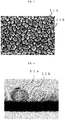
FIG. 3 is SEM image of a metal layer in one embodiment of the present invention. -
FIG. 4 is TEM image of a cross-section of a metal layer in one embodiment of the present invention. -
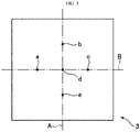
FIG. 5 is a view showing measurement points of a thickness of the metal layer in the examples. - Embodiments for carrying out the present invention are described in detail below. However, the present invention is not construed as being limited to the embodiments described below.
- Schematic cross-sectional view of the electromagnetic wave transmissive metallic luster film (hereinafter simply referred to as a "metallic luster film") 1 according to one embodiment of the present invention is shown in
FIG. 1 . Themetallic luster film 1 of this embodiment includes asubstrate film 10, ametal layer 11 which is formed on thesubstrate film 10 and is a discontinuous layer containing a metal, and an adhesive layer 12 which is formed on themetal layer 11 and is a layer containing a transparent adhesive. -
FIG. 2 is a schematic cross-sectional view of the state that themetallic luster film 1 according to one embodiment of the present invention is adhered to anadherend 2. Since themetallic luster film 1 of this embodiment has the above configuration, even in the case where the film is used by adhering to a surface 2b on the side (hereinafter sometimes referred to as "inside") opposite a surface 2a of the visually recognized side (hereinafter sometimes referred to as "outside") of atransparent adherend 2 via the adhesive layer 12, themetal layer 11 can be visually recognized through theadherend 2 and the adhesive layer 12. In other words, themetallic luster film 1 can decorate thetransparent adherend 2 from the inside. - By adhering the
metallic luster film 1 of this embodiment to the inside of theadherend 2, the film is not brought into contact with the outside of a product that is obtained by adhering themetallic luster film 1 of this embodiment to theadherend 2 and is thus scratch-resistant. Additionally, the film can decorate theadherend 2 while utilizing the original texture of theadherend 2. - The
substrate film 10 that can be used includes films including a homopolymer or a copolymer such as polyethylene terephthalate (PET), polyethylene naphthalate (PEN), polybutylene terephthalate, polyamide, polyvinyl chloride, polycarbonate (PC), cycloolefin polymer (COP), polystyrene, polypropylene (PP), polyethylene, polycycloolefin, polyurethane, acryl (PMMA) and ABS. Those members do not affect brilliancy and electromagnetic wave transmitting property. However, to form themetal layer 11 later, thesubstrate film 10 is preferably films that can withstand high temperature such as deposition or sputtering. Therefore, of the above materials, polyethylene terephthalate, polyethylene naphthalate, acryl, polycarbonate, cycloolefin polymer, ABS, polypropylene and polyurethane are preferred. Above all, polyethylene terephthalate, cycloolefin polymer, polycarbonate and acryl are preferred from good balance between heat resistance and costs. Thesubstrate film 10 may be a single layer film and may be a laminate film. The thickness of thesubstrate film 10 is preferably, for example, about 6 µm to 250 µm from easy processing and the like. Furthermore, plasma treatment, easy adhesion processing or the like may be applied to thesubstrate film 10 in order to increase adhesion to the metal layer and an indium oxide-containing layer described hereinafter. Furthermore, thesubstrate film 10 may have a light-shielding property, although the detail is described hereinafter. - The
metal layer 11 is a discontinuous layer containing a metal, which is formed on thesubstrate film 10. - The metal constituting the
metal layer 11 in this embodiment is not particularly limited. For example, at least one metal selected from aluminum (Al), zinc (Zn), lead (Pb), copper (Cu) and silver (Ag), and an alloy containing the metal as a main component can be used. - The
metallic luster film 1 of this embodiment has metallic luster due to themetal layer 11 and can impart an appearance of high-quality feeling to the adherend. A metal having high reflectance in a visible light region is preferably used in the metal constituting themetal layer 11 from the standpoint of the improvement of the high-quality feeling, and aluminum or an aluminum alloy is preferably used from this standpoint. In the case of using an aluminum alloy, the content of aluminum is preferably 50 wt% or more. - The
metal layer 11 in this embodiment only needs to have a discontinuous structure having metal parts 11a and a gap 11b, and has, for example, an island structure or a crack structure described hereinafter. Themetallic luster film 1 of this embodiment has electromagnetic wave transmitting property due to the presence of the gap 11b in themetal layer 11. As a result, themetallic luster film 1 of this embodiment can be suitably used in the decoration of a device sending and receiving radio wave, such as mobile phones or smart phones. - The island structure is a structure in which metal particles are independent to each other, are slightly separated from each other or are laid in the state of partially contacting with each other. SEM image of the
metal layer 11 having an island structure in one embodiment of the present invention is shown inFIG. 3 . Furthermore, TEM image of a cross-sectional view of themetal layer 11 having an island structure in one embodiment of the present invention is shown inFIG. 4 . - The
metal layer 11 having an island structure can be formed by, for example, depositing or sputtering a metal on thesubstrate film 10. In this case, when an indium oxide-containing layer is previously provided on thesubstrate film 10, themetal layer 11 having an island structure can be easily obtained and this is preferred. The detail of the indium oxide-containing layer is described hereinafter. - The thickness of the
metal layer 11 having an island structure is not particularly limited, but is preferably 20 nm or more and more preferably 30 nm or more from the standpoint of the improvement of metallic luster feeling. - On the other hand, the thickness is preferably 100 nm or less and more preferably 70 nm or less from the standpoint of the improvement of electromagnetic wave transmitting property.
- The thickness of the
metal layer 11 in the present description means the value measured by the method described in the item of "Examples". - The equivalent circle diameter of the metal part 11a in the
metal layer 11 having an island structure is not particularly limited, but is generally about 10 to 1000 nm. Furthermore, the distance between the metal parts 11a is not particularly limited, but is generally about 10 to 1000 nm. - The crack structure is a structure in which a metal thin film is divided by cracks.
- The
metal layer 11 of the crack structure can be formed by, for example, providing a metal thin film on thesubstrate film 10, and bending and stretching, thereby generating cracks in the metal thin film. In this case, themetal layer 11 having a crack structure can be easily formed by providing a brittle layer formed of a material having poor stretchability, that is, a material easily forming cracks by stretching, between thesubstrate film 10 and the metal thin film. - As described above, embodiments in which the
metal layer 11 is discontinuous are not particularly limited, but an island structure is preferred from the standpoint of productivity. - The adhesive layer 12 is a layer containing a transparent adhesive, which is formed on the
metal layer 11. Themetallic luster film 1 of this embodiment is used by adhering to theadherend 2 through the adhesive layer 12. - An adhesive forming the adhesive layer 12 is not particularly limited so long as it is a transparent adhesive. For example, an acrylic adhesive, a rubber adhesive, a silicone adhesive, a polyester adhesive, a urethane adhesive, an epoxy adhesive and a polyether adhesive can be used alone or as mixtures of two or more kinds. The acrylic adhesive is preferably used from the standpoints of transparency, processability, durability and the like.
- The thickness of the adhesive layer 12 is not particularly limited. Small thickness can improve visible light transmitting property, film thickness precision and flatness. Therefore, the thickness is preferably 100 µm or less, more preferably 75 µm or less and still more preferably 50 µm or less.
- The total light transmittance of the whole adhesive layer 12 is not particularly limited, but is preferably 10% or more, more preferably 30% or more and still more preferably 50% or more, as the value in optional visible light wavelength measured according to JIS K7361. Higher total light transmittance of the adhesive layer 12 is preferred.
- The transparent adhesive constituting the adhesive layer 12 may be colored.
- In this case, the
metal layer 11 is viewed through the colored adhesive layer 12, and as a result, colored metallic luster can be expressed. - In general, in the case of expressing colored metallic luster, a layer for coloring should be provided separately, and this increases the overall thickness of the metallic luster film. However, use of the colored transparent adhesive can express colored metallic luster without involving the increase of the thickness.
- The
metallic luster film 1 of this embodiment is used by adhering to the inside of theadherend 2. In the case where theadherend 2 is a casing substrate of precision equipment such as mobile phones and smart phones, smaller thickness of themetallic luster film 1 is preferred in order to suppress the space in the casing from being oppressed. Therefore, in the case of expressing colored metallic luster using themetallic luster film 1 of this embodiment, colored transparent adhesive is preferably used. - A method of coloring the transparent adhesive is not particularly limited. For example, the transparent adhesive can be colored by adding a slight amount of a colorant.
- A release liner is preferably provided on the adhesive layer 12 in order to protect the adhesive layer 12 until adhering to the
adherend 2. - The
metallic luster film 1 of the present invention may have layers other than thesubstrate film 10, themetal layer 11 and the adhesive layer 12 so long as the effect of the present invention is achieved. For example, the metallic luster film may have the layers exemplified below. - The
metallic luster film 1 of this embodiment may have a light-shielding layer having no visible light transmitting property on the surface of thesubstrate film 10 that is opposite the surface thereof on which themetal layer 11 is formed. When the light-shielding layer is provided, for example, in the case where themetallic luster film 10 of this embodiment is used in decoration of a casing of electronic devices, a circuit in the casing can be prevented from being viewed through themetallic luster film 1. - Material of the light-shielding layer is not particularly limited, and for example, the materials exemplified as the materials that can be used in the
substrate film 10 described before is colored in black and can be used. - Even in the metallic luster film having no light-shielding layer, the same effect as the case of having the light-shielding layer can be achieved by making the
substrate film 10 light-shielding. - The
metallic luster film 1 of this embodiment may have an indium oxide-containing layer between thesubstrate film 10 and themetal layer 11. When the indium oxide-containing layer is present between thesubstrate film 10 and themetal layer 11, that is, the indium oxide-containing layer is formed on thesubstrate film 10 and themetal layer 11 is then formed thereon, themetal layer 11 having an island structure is easily formed by sputtering. - The indium oxide-containing layer may be directly provided on the surface of the
substrate film 10 and may be indirectly provided on the surface of thesubstrate film 10 through a protective layer or the like. The indium oxide-containing layer is preferably provided on the surface of thesubstrate film 10 in a continuous state, that is, without a gap. By providing the indium oxide-containing layer in a continuous state, smoothness and corrosion resistance of the indium oxide-containing layer, eventually, themetal layer 11 and themetallic luster film 1, can be improved, and furthermore, the indium oxide-containing layer is easily film-formed without in-plane fluctuation. - Indium oxide (In2O3) itself can be used as the indium oxide-containing layer, and, for example, a metal-containing material such as indium tin oxide (ITO) or indium zinc oxide (IZO) can be used as the indium oxide-containing layer. ITO or IZO that contains a metal other than indium is more preferably used from that discharge stability in sputtering is high.
- The content of tin (Sn) to the weight of In2O3 in ITO is not particularly limited, but is, for example, 2.5 wt% to 30 wt% and more preferably 3 wt% to 10 wt%. The content of zinc oxide (ZnO) to the weight of In2O3 in IZO is, for example, 2 wt% to 20 wt%.
- As described above, aluminum or an aluminum alloy is preferably used in the
metal layer 11 in themetallic luster film 1 of this embodiment. However, aluminum or an aluminum alloy has been difficult to form an island structure, different from indium, tin and the like. In other words, when aluminum or an aluminum alloy was laminated on thesubstrate film 10 by sputtering, a continuous metal layer is liable to be formed. - On the other hand, a discontinuous layer of aluminum can be relatively easily obtained by forming an indium oxide-containing layer on the
substrate film 10 and then laminating aluminum or an aluminum alloy thereon by sputtering. - The mechanism that the
metal layer 11 having a discontinuous structure can be easily obtained by providing the indium oxide-containing layer onto thesubstrate film 10 is not yet clear, but it is assumed to be as follows. - In a thin film forming process of the
metal layer 11, easiness of the formation of a discontinuous structure has the correlation with surface diffusion on an object member to which themetal layer 11 is given (in this embodiment, the indium oxide-containing layer formed on the substrate film 10), and a discontinuous structure is easily formed as the temperature of the object member is high, wettability of the metal layer to the object member is small and a melting point of the material of themetal layer 11 is low. In other words, the indium oxide-containing layer has small wettability to a metal as compared with thesubstrate film 10. Therefore, it is considered that themetal layer 11 having a discontinuous structure is easy to be formed by forming the indium oxide-containing layer on thesubstrate film 10. - Furthermore, regarding metals other than aluminum (Al) particularly used in the examples mentioned later, it is considered that a metal having relatively low melting point, such as zinc (Zn), lead (Pb), copper (Cu) or silver (Ag), can easily form a discontinuous structure in the same method.
- The thickness of the indium oxide-containing layer is generally preferably 1000 nm or less, more preferably 50 nm or less and still more preferably 20 nm or less, from the standpoints of electromagnetic wave transmission property and productivity. On the other hand, the thickness of the indium oxide-containing layer is preferably 1 nm or more such that the
metal layer 11 to be laminated becomes easy to be a discontinuous state, more preferably 2 nm or more in order to certainly become a discontinuous state and still more preferably 5 nm or more. - The ratio between the thickness of the
metal layer 11 and the thickness of the indium oxide-containing layer (thickness ofmetal layer 11/thickness of indium oxide-containing layer) is preferably a range of 0.1 to 100 and more preferably a range of 0.3 to 35. - The indium oxide-containing layer can be formed by vacuum deposition, sputtering, ion plating or the like, but is preferably formed by sputtering from that the thickness can be strictly controlled even though large area.
- Properties of the
metallic luster film 1 of this embodiment are described below. - The value of sheet resistance of the
metallic luster film 1 of this embodiment is not particularly limited. In the case where the metallic luster sheet is used in a device sending and receiving radio wave, the film preferably has excellent electromagnetic wave transmitting property. From this standpoint, the value of sheet resistance is preferably 100 Ω/square or more and more preferably 200 Ω/square or more. - The sheet resistance value of the
metallic luster film 1 can be measured by an eddy current measurement method according to JIS Z2316-1: 2014. - The value of electromagnetic wave transmission attenuation of the
metallic luster film 1 of this embodiment is not particularly limited. However, in case of using the film in the decoration of a device sending and receiving radio wave, the value is preferably small. For example, microwave electric field transmission attenuation measured by the method described in the item of Examples is preferably 10 [-dB] or less and more preferably 5 [-dB] or less. - The electromagnetic wave transmitting property in microwave band (1 GHz) has the correlation with the electromagnetic wave transmitting property in frequency band (76 to 80 GHz) of millimeter wave radar, and those properties show relatively near value. Therefore, the metallic luster film having small microwave electric field transmission attenuation and excellent electromagnetic wave transmitting property in microwave band also has excellent electromagnetic wave transmitting property in frequency band of millimeter wave radar, as described above.
- The visible light reflectance of the
metallic luster film 1 of this embodiment is not particularly limited, but metallic luster feeling is excellent as the visible light reflectance is large. Thus, larger visible light reflectance is preferred. Therefore, in the metallic luster film of this embodiment, for example, the reflectance in a wavelength of 550 nm is preferably 20% or more, more preferably 40% or more and still more preferably 50% or more, when the reflectance of Al-deposited mirror measured according to the method described in the item of Examples is 100% as a reference. - The thickness of the
metallic luster film 10 of this embodiment is not particularly limited. However, in the case where theadherend 2 is, for example, a casing of precision devices such as mobile phones or smart phones, the thickness of the metallic luster film is preferably small as described before. Therefore, the thickness of themetallic luster film 1 of this embodiment is preferably 300 µm or less, more preferably 200 µm or less and still more preferably 100 µm or less. - A method of adhering the
metallic luster layer 1 of this embodiment to theadherend 2 is not particularly limited. For example, the film can be adhered by vacuum forming. The vacuum forming is a method of stretching a film while heating and softening, reducing a pressure in a space in the adherend side of the film, pressuring a space in the opposite side as required, and adhering and laminating while forming the film along a three-dimensional shape of the surface of the adherend. - The
metallic luster film 1 of this embodiment is used by adhering to the inside surface of thetransparent adherend 2. As thetransparent adherend 2, a member formed of glass or plastics can be used, but is not limited to those. - The
metallic luster film 1 of this embodiment has electromagnetic wave transmitting property and therefore can be suitably used in the decoration of an exterior member of a device sending and receiving radio wave. For example, a casing obtained by adhering the metallic luster film of this embodiment to the inside surface of a transparent casing substrate can be suitably used as a casing of electronic instruments such as mobile phones, smart phones and computers. - The present invention is described below by reference to examples, but is not construed as being limited to those.
- ITO layer having a thickness of 5 nm was directly formed on PET film O-300E having a thickness 125 µm manufactured by Mitsubishi Chemical Corporation (hereinafter referred to as a substrate film) using DC magnetron sputtering. The temperature of the substrate film when forming the ITO film was set to 130°C. ITO contains SnO2 in an amount of 10 wt% based on In2O3.
- An island-shaped aluminum (Al) layer having a thickness of 50 nm was formed on the ITO layer using AC sputtering (AC: 40 kHz), thereby obtaining a laminate of the substrate film, the indium oxide-containing layer and the metal layer (Al) layer (hereinafter referred to as the laminate). The temperature of the substrate film in forming the Al layer was set to 130°C.
- The thickness of the Al layer is an average value of the thickness of the metal parts 11a measured as follows, considering the variation of the thickness in the layer, in more detail, the variation of the thickness of every metal part 11a. The average value is hereinafter called "the maximum thickness" for convenience.
- A square region 3 having one side of 5 cm as shown in
FIG. 5 was appropriately extracted from the laminate, and the total points "a" to "e" obtained by dividing the respective center lines A and B of the vertical side and the horizontal side of the square region 3 into 4 equal parts were selected as the measurement points. - Cross-sectional image as shown in
FIG. 4 in the respective measurement points selected was measured, and a viewing angle area containing about five metal parts 11a was extracted from the TEM image obtained. Individual thicknesses of the metal parts 11a, that is, individual thickness of about 25 (about 5 × 5) metal parts 11a, in the viewing angle area extracted in the five measurement points were obtained from the TEM image, and the average value of those was designated as the thickness of the Al layer. - The thickness of each metal part 11a was the thickness in the thickest part in a vertical direction from the ITO layer.
- A monomer mixture containing 100 parts by mass of butyl acrylate, 0.01 parts by mass of 2-hydoxyethyl acrylate and 5 parts of acrylic acid were placed in a reaction vessel equipped with a cooling pipe, a nitrogen inlet pipe, a thermometer and a stirring apparatus. 2,2'-Azobisisobutyronitrile as a polymerization initiator in an amount of 0.1 part by mass per 100 parts by mass of the monomer mixture was placed in the reaction vessel together with 100 parts by mass of ethyl acetate, and nitrogen gas was introduced while gently stirring to perform nitrogen substitution. Liquid temperature in the reaction vessel was maintained in the vicinity of 55°C and a polymerization reaction was conducted for 8 hours. Thus, an acrylic polymer solution (solid content concentration 30 wt%) having a weight average molecular weight (Mw): 1,800,000 and Mw/Mn=4.1 was prepared.
- 0.3 Parts by mass of benzoyl peroxide (NYPER BMT manufactured by NOF Corporation), 1 part by mass of an isocyanate crosslinking agent (CORONATE L manufactured by Tosoh Corporation) and 0.25 parts by mass of a tetraazaporphyrin dye (PD-320, having maximum absorption wavelength at wavelength of 595 nm, manufactured by Yamamoto Chemicals Inc.) were added to 100 parts by mass of the solid content of the acrylic polymer solution obtained, and a colored adhesive composition was obtained. The colored adhesive composition obtained was dried at 130°C for 2 minutes, and a colored adhesive sheet having a thickness of 25 µm was obtained.
- The colored adhesive sheet obtained above was applied to the metal layer side-surface of the laminate obtained above by a hand roller to form an adhesive layer. Thus, a metallic luster film of Example 1 having colored metallic luster was obtained.
- Metallic luster film of Example 2 was obtained in the same manner as in Example 1, except for using a colored adhesive sheet obtained as follows.
- A monomer mixture containing 100 parts by mass of butyl acrylate, 0.01 parts by mass of 2-hydoxyethyl acrylate and 5 parts of acrylic acid were placed in a reaction vessel equipped with a cooling pipe, a nitrogen inlet pipe, a thermometer and a stirring apparatus. 2,2'-Azobisisobytyronitrile as a polymerization initiator in an amount of 0.1 parts by mass per 100 parts by mass of the monomer mixture was placed in the reaction vessel together with 100 parts by mass of ethyl acetate, and nitrogen gas was introduced while gently stirring to perform nitrogen substitution. Liquid temperature in the reaction vessel was maintained in the vicinity of 55°C and a polymerization reaction was conducted for 8 hours. Thus, an acrylic polymer solution (solid content concentration 30 wt%) having a weight average molecular weight (Mw): 1,800,000 and Mw/Mn=4.1 was prepared.
- 0.3 Parts by mass of benzoyl peroxide (NYPER BMT manufactured by NOF Corporation), 1 part by mass of an isocyanate crosslinking agent (CORONATE L manufactured by Tosoh Corporation), AJISPER PB821 manufactured by Ajinomoto Fine-Techno Co., Inc. as a dispersant and 0.05 parts by mass of Pigment Blue 15 (manufactured by Tokyo Chemical Industry Co., Ltd.) as a pigment were added to 100 parts by mass of the solid content of the acrylic polymer solution obtained, and a colored adhesive composition was obtained. The colored adhesive composition obtained was dried at 130°C for 2 minutes, and a colored adhesive sheet having a thickness of 25 µm was obtained.
- Metallic luster film of Example 3 was prepared in the same manner as in Example 2, except that the amount of Pigment Blue 15 added was changed to 0.1 parts by mass.
- Metallic luster film of Example 4 was prepared in the same manner as in Example 2, except that the amount of Pigment Blue 15 added was changed to 0.5 parts by mass.
- Metallic luster film of Example 5 was prepared in the same manner as in Example 2, except that the amount of Pigment Blue 15 added was changed to 1.0 part by mass.
- Metallic luster film of Example 6 was prepared in the same manner as in Example 2, except that the amount of Pigment Blue 15 added was changed to 2.5 parts by mass.
- Metallic luster film of Example 7 was prepared in the same manner as in Example 2, except that Pigment Yellow 74 (Dalamar Yellow manufactured by Oakwood Products, Inc.) was added as a pigment in an amount of 0.05 parts by mass in place of Pigment Blue 15.
- Metallic luster film of Example 8 was prepared in the same manner as in Example 7, except that the amount of Pigment Yellow 74 added was changed to 0.1 parts by mass.
- Metallic luster film of Example 9 was prepared in the same manner as in Example 7, except that the amount of Pigment Yellow 74 added was changed to 0.5 parts by mass.
- Metallic luster film of Example 10 was prepared in the same manner as in Example 7, except that the amount of Pigment Yellow 74 added was changed to 1.0 part by mass.
- Metallic luster film of Example 11 was prepared in the same manner as in Example 7, except that the amount of Pigment Yellow 74 added was changed to 2.5 parts by mass.
- Spectrophotometer U4100 manufactured by Hitachi High-Technologies was used. The colored adhesive sheet obtained was adhered to a blue glass sheet having a thickness of 1.2 mm, total light transmittance at 380 to 780 nm was measured with 5 nm pitch, and the maximum value of the transmittance, the average value of 5 nm pitch and the minimum value were obtained. The results are shown in Table 1.
[Table 1] Coloring matter/pigment Dispersant Visible light transmittance (%) Material Concentration (parts by mass) Material Maximum Average Minimum Ex. 1 PD-320 0.25 - 91 80 10 Ex. 2 Pigment Blue 15 0.05 AJISPER PB821 87 77 65 Ex. 3 Pigment Blue 15 0.1 AJISPER PB821 86 69 51 Ex. 4 Pigment Blue 15 0.5 AJISPER PB821 82 39 8 Ex. 5 Pigment Blue 15 1 AJISPER PB821 77 28 2 Ex. 6 Pigment Blue 15 2.5 AJISPER PB821 63 16 0 Ex. 7 Pigment Yellow 74 0.05 AJISPER PB821 83 83 64 Ex. 8 Pigment Yellow 74 0.1 AJISPER PB821 80 80 49 Ex. 9 Pigment Yellow 74 0.5 AJISPER PB821 68 68 3 Ex. 10 Pigment Yellow 74 1 AJISPER PB821 64 64 2 Ex. 11 Pigment Yellow 74 2.5 AJISPER PB821 57 57 0 - Sheet resistance of the metallic luster film of Example 1 was measured by an eddy current measurement method according to JIS Z2316-1: 2014 using a non-contact type resistance measurement instrument NC-80MAP manufactured by Napson Corporation. As a result, the sheet resistance was 4830 Ω/square.
- Radio wave transmission attenuation at 1 GHz of the metallic luster film of Example 1 was evaluated using KEC method measurement evaluation jig and a spectrum analyzer CXA signal Analyzer NA9000A manufactured by Agilent Technologies. As a result, the transmission attenuation was 0.02 [-dB].
- Regular reflectance at a measurement wavelength of 550 µm of the metallic luster film of Example 1 was measured using a spectrophotometer U4100 manufactured by Hitachi High-Technologies. As a result, the regular reflectance was 55%. Reflectance of Al-deposited mirror was considered to be reflectance 100% as a reference.
- As described above, the metallic luster films of the examples had sufficiently high sheet resistance value and showed good results of radio wave transmission attenuation. Therefore, the metallic luster films had excellent electromagnetic wave transmitting property. Furthermore, the metallic luster films of the examples have excellent visible light reflectance and therefore have metallic luster of high-quality feeling.
- Although the present invention has been described in detail and by reference to the specific embodiments, it is apparent to one skilled in the art that various modifications or changes can be made without departing the spirit and scope of the present invention. This application is based on Japanese Patent Application No.
2018-3790 filed January 12, 2018 2018-82506 filed April 23, 2018 -
- 1:
- Metallic luster film
- 10:
- Substrate film
- 11:
- Metal layer
- 11a:
- Metal part
- 11b:
- Gap
- 12:
- Adhesive layer
- 2:
- Adherend
- 2a:
- Surface of visually recognized side (outside)
- 2b:
- Surface (inside) opposite visually recognized surface (outside)
Claims (12)
- An electromagnetic wave transmissive metallic luster film comprising a substrate film, a metal layer formed on one surface of the substrate film and an adhesive layer formed on the metal layer,
wherein the metal layer is a discontinuous layer comprising a metal, and
the adhesive layer is a layer comprising a transparent adhesive. - The electromagnetic wave transmissive metallic luster film according to claim 1, which further comprises an indium oxide-containing layer between the substrate film and the metal layer.
- The electromagnetic wave transmissive metallic luster film according to claim 2, wherein the indium oxide-containing layer is provided in a continuous state.
- The electromagnetic wave transmissive metallic luster film according to any one of claims 1 to 3, wherein the transparent adhesive is colored.
- The electromagnetic wave transmissive metallic luster film according to any one of claims 1 to 4, wherein the metal layer has an island structure.
- The electromagnetic wave transmissive metallic luster film according to any one of claims 1 to 5, wherein the metal layer comprises aluminum or an aluminum alloy.
- The electromagnetic wave transmissive metallic luster film according to claim 6, wherein the aluminum alloy contains aluminum in an amount of 50 wt% or more.
- The electromagnetic wave transmissive metallic luster film according to any one of claims 1 to 7, which comprises a light-shielding layer formed on a surface of the substrate layer that is opposite the surface thereof on which the metal layer is formed.
- The electromagnetic wave transmissive metallic luster film according to any one of claims 1 to 7, wherein the substrate film has light-shielding property.
- The electromagnetic wave transmissive metallic luster film according to any one of claims 1 to 9, which is used by adhering, via the adhesive layer, to a surface of a transparent member that is opposite a visually recognized surface thereof.
- A casing comprising a transparent casing substrate and the electromagnetic wave transmissive metallic luster film of according to any one of claims 1 to 10,
wherein the electromagnetic wave transmissive metallic luster film is adhered, via the adhesive layer, to a surface of the transparent casing substrate that is opposite a visually recognized surface thereof. - An electronic device comprising the casing according to claim 11.
Applications Claiming Priority (3)
| Application Number | Priority Date | Filing Date | Title |
|---|---|---|---|
| JP2018003790 | 2018-01-12 | ||
| JP2018082506 | 2018-04-23 | ||
| PCT/JP2019/000799 WO2019139154A1 (en) | 2018-01-12 | 2019-01-11 | Electromagnetic wave transmissive metallic luster film |
Publications (2)
| Publication Number | Publication Date |
|---|---|
| EP3738766A1 true EP3738766A1 (en) | 2020-11-18 |
| EP3738766A4 EP3738766A4 (en) | 2021-10-20 |
Family
ID=67219590
Family Applications (1)
| Application Number | Title | Priority Date | Filing Date |
|---|---|---|---|
| EP19738582.6A Pending EP3738766A4 (en) | 2018-01-12 | 2019-01-11 | ELECTROMAGNETIC WAVES TRANSMITTING METALLIC GLOSS FOIL |
Country Status (6)
| Country | Link |
|---|---|
| US (1) | US20210078289A1 (en) |
| EP (1) | EP3738766A4 (en) |
| JP (1) | JP7332298B2 (en) |
| KR (1) | KR20200105836A (en) |
| CN (1) | CN111629893A (en) |
| WO (1) | WO2019139154A1 (en) |
Families Citing this family (3)
| Publication number | Priority date | Publication date | Assignee | Title |
|---|---|---|---|---|
| JP2021024251A (en) * | 2019-08-08 | 2021-02-22 | 日東電工株式会社 | Electromagnetic wave transmissible laminate |
| US11339495B2 (en) * | 2020-05-20 | 2022-05-24 | Toyota Motor Engineering & Manufacturing North America, Inc. | Coated discrete metallic particles and multilayer structures comprising reflective core layers |
| CN114635113B (en) * | 2022-03-09 | 2023-04-07 | 北京科技大学 | Preparation method of high-brightness silvery white electromagnetic wave transmission composite film |
Family Cites Families (15)
| Publication number | Priority date | Publication date | Assignee | Title |
|---|---|---|---|---|
| JP3951740B2 (en) * | 2002-02-26 | 2007-08-01 | 豊田合成株式会社 | Manufacturing method of radio wave transmission cover |
| JP2006264315A (en) * | 2005-02-28 | 2006-10-05 | Seiko Epson Corp | Ornaments and watches |
| JP2006281591A (en) * | 2005-03-31 | 2006-10-19 | Nissha Printing Co Ltd | Decorative sheet with metallic gloss and decorative molding using the sheet |
| JP3802041B1 (en) * | 2005-05-25 | 2006-07-26 | 三菱樹脂株式会社 | Laminate for producing nameplates that can prevent fluctuations in reflected light |
| KR101403931B1 (en) * | 2005-08-18 | 2014-06-09 | 도레이 카부시키가이샤 | Laminate film and molded article |
| JP4706596B2 (en) * | 2005-10-31 | 2011-06-22 | 豊田合成株式会社 | Resin product, method for producing the same, and method for forming metal film |
| JP5339700B2 (en) * | 2007-09-14 | 2013-11-13 | 日本写真印刷株式会社 | Radio wave transmitting transfer material and manufacturing method thereof |
| JP2009090507A (en) * | 2007-10-05 | 2009-04-30 | Nissha Printing Co Ltd | Decorative sheet, its manufacturing method, and decorative molded article |
| JP5400454B2 (en) * | 2009-04-13 | 2014-01-29 | 三恵技研工業株式会社 | Method for producing electromagnetically permeable metal composite material |
| KR101377393B1 (en) | 2011-01-13 | 2014-03-25 | (주)엘지하우시스 | Metal-colored and non-conductive transfer film |
| WO2014126135A1 (en) * | 2013-02-13 | 2014-08-21 | 東洋紡株式会社 | Heat ray-reflecting, radio wave-transmitting transparent laminate |
| JPWO2015025963A1 (en) * | 2013-08-23 | 2017-03-02 | 王子ホールディングス株式会社 | Heat ray shielding material |
| WO2016125823A1 (en) * | 2015-02-03 | 2016-08-11 | 王子ホールディングス株式会社 | Heat shielding film, and heat shielding laminated glass and method for manufacturing same |
| JP6380473B2 (en) | 2016-07-07 | 2018-08-29 | トヨタ自動車株式会社 | Intake manifold |
| JP2018082506A (en) | 2016-11-14 | 2018-05-24 | 株式会社オートネットワーク技術研究所 | Dc-dc converter |
-
2019
- 2019-01-11 EP EP19738582.6A patent/EP3738766A4/en active Pending
- 2019-01-11 WO PCT/JP2019/000799 patent/WO2019139154A1/en not_active Ceased
- 2019-01-11 KR KR1020207019519A patent/KR20200105836A/en not_active Withdrawn
- 2019-01-11 JP JP2019003813A patent/JP7332298B2/en active Active
- 2019-01-11 CN CN201980008009.8A patent/CN111629893A/en active Pending
- 2019-09-11 US US16/961,447 patent/US20210078289A1/en not_active Abandoned
Also Published As
| Publication number | Publication date |
|---|---|
| US20210078289A1 (en) | 2021-03-18 |
| JP7332298B2 (en) | 2023-08-23 |
| CN111629893A (en) | 2020-09-04 |
| EP3738766A4 (en) | 2021-10-20 |
| JP2019188798A (en) | 2019-10-31 |
| KR20200105836A (en) | 2020-09-09 |
| WO2019139154A1 (en) | 2019-07-18 |
Similar Documents
| Publication | Publication Date | Title |
|---|---|---|
| JP6400062B2 (en) | Electromagnetic wave transmitting metallic luster member, article using the same, and metallic thin film | |
| JP7319079B2 (en) | Electromagnetic wave permeable metallic luster article and decorative member | |
| EP3738766A1 (en) | Electromagnetic wave transmissive metallic luster film | |
| US11577491B2 (en) | Metallic lustrous member with radio wave transmissibility, article using same, and production method therefor | |
| WO2021025054A1 (en) | Electromagnetic wave transmissive layered product | |
| JP7319077B2 (en) | Electromagnetic wave transparent metallic luster article and metal thin film | |
| WO2019208493A1 (en) | Electromagnetic-wave-permeable metallic-luster article, and decorative member | |
| WO2019208504A1 (en) | Electromagnetic wave transparent metallic luster article, and metal thin film | |
| WO2021006130A1 (en) | Electromagnetic wave transmitting metallic luster article | |
| WO2019208499A1 (en) | Electromagnetically permeable article with metallic gloss | |
| JP7319081B2 (en) | Electromagnetic wave permeable metallic luster article | |
| TW202120323A (en) | Multilayer body | |
| WO2021182380A1 (en) | Electromagnetic-wave-transmissive laminated member and method for manufacturing same | |
| JP2019123224A (en) | Electromagnetic Wave Permeable Half Mirror Film | |
| JP7670684B2 (en) | Electromagnetic wave transparent metallic glossy material | |
| WO2019208488A1 (en) | Electromagnetic wave transmissive metal luster article | |
| JP2019188809A (en) | Electromagnetic wave transmissible metallic sheen article | |
| JP2022131590A (en) | Metallic sheen member, decorative member, and manufacturing method of metallic sheen member | |
| JP2023013743A (en) | Laminate and decorative member | |
| WO2019139122A1 (en) | Radio wave-transmitting lustrous metal member, article using same, and method for producing same | |
| WO2019208494A1 (en) | Electromagnetic wave transmissive metallic luster product and metal thin film | |
| JP2006120916A (en) | Transparent conductive laminate, and filter for display using the same | |
| WO2022181528A1 (en) | Electromagnetically permeable member with metallic gloss, and decorative member | |
| WO2022004671A1 (en) | Electromagnetic wave-permeable metallic luster member, and decorative member | |
| WO2021200292A1 (en) | Layered body, electromagnetic wave permeable layered body, and article |
Legal Events
| Date | Code | Title | Description |
|---|---|---|---|
| STAA | Information on the status of an ep patent application or granted ep patent |
Free format text: STATUS: THE INTERNATIONAL PUBLICATION HAS BEEN MADE |
|
| PUAI | Public reference made under article 153(3) epc to a published international application that has entered the european phase |
Free format text: ORIGINAL CODE: 0009012 |
|
| STAA | Information on the status of an ep patent application or granted ep patent |
Free format text: STATUS: REQUEST FOR EXAMINATION WAS MADE |
|
| 17P | Request for examination filed |
Effective date: 20200708 |
|
| AK | Designated contracting states |
Kind code of ref document: A1 Designated state(s): AL AT BE BG CH CY CZ DE DK EE ES FI FR GB GR HR HU IE IS IT LI LT LU LV MC MK MT NL NO PL PT RO RS SE SI SK SM TR |
|
| AX | Request for extension of the european patent |
Extension state: BA ME |
|
| DAV | Request for validation of the european patent (deleted) | ||
| DAX | Request for extension of the european patent (deleted) | ||
| REG | Reference to a national code |
Ref country code: DE Ref legal event code: R079 Free format text: PREVIOUS MAIN CLASS: B32B0015040000 Ipc: C08J0007040000 |
|
| A4 | Supplementary search report drawn up and despatched |
Effective date: 20210921 |
|
| RIC1 | Information provided on ipc code assigned before grant |
Ipc: B32B 27/36 20060101ALI20210915BHEP Ipc: B32B 27/30 20060101ALI20210915BHEP Ipc: B32B 27/08 20060101ALI20210915BHEP Ipc: C09J 7/22 20180101ALI20210915BHEP Ipc: C08J 7/04 20200101AFI20210915BHEP |
|
| STAA | Information on the status of an ep patent application or granted ep patent |
Free format text: STATUS: EXAMINATION IS IN PROGRESS |
|
| 17Q | First examination report despatched |
Effective date: 20250115 |