EP3738207B1 - Low quiescent current load switch - Google Patents
Low quiescent current load switch Download PDFInfo
- Publication number
- EP3738207B1 EP3738207B1 EP19738707.9A EP19738707A EP3738207B1 EP 3738207 B1 EP3738207 B1 EP 3738207B1 EP 19738707 A EP19738707 A EP 19738707A EP 3738207 B1 EP3738207 B1 EP 3738207B1
- Authority
- EP
- European Patent Office
- Prior art keywords
- gate
- current
- voltage
- charge pump
- load switch
- Prior art date
- Legal status (The legal status is an assumption and is not a legal conclusion. Google has not performed a legal analysis and makes no representation as to the accuracy of the status listed.)
- Active
Links
- 239000003990 capacitor Substances 0.000 claims description 48
- 239000004065 semiconductor Substances 0.000 claims description 6
- 230000007423 decrease Effects 0.000 description 8
- 238000010586 diagram Methods 0.000 description 8
- 230000008859 change Effects 0.000 description 7
- 239000013256 coordination polymer Substances 0.000 description 6
- 230000008901 benefit Effects 0.000 description 5
- 230000000694 effects Effects 0.000 description 5
- 238000000034 method Methods 0.000 description 5
- 230000004913 activation Effects 0.000 description 4
- 238000001514 detection method Methods 0.000 description 4
- 238000013459 approach Methods 0.000 description 3
- 230000000295 complement effect Effects 0.000 description 3
- 238000013461 design Methods 0.000 description 3
- 238000007667 floating Methods 0.000 description 3
- 238000012163 sequencing technique Methods 0.000 description 3
- 230000008569 process Effects 0.000 description 2
- 230000009286 beneficial effect Effects 0.000 description 1
- 230000000903 blocking effect Effects 0.000 description 1
- 238000004891 communication Methods 0.000 description 1
- 230000003247 decreasing effect Effects 0.000 description 1
- 230000001419 dependent effect Effects 0.000 description 1
- 238000011161 development Methods 0.000 description 1
- 230000009977 dual effect Effects 0.000 description 1
- 230000005611 electricity Effects 0.000 description 1
- 238000005516 engineering process Methods 0.000 description 1
- 230000005669 field effect Effects 0.000 description 1
- 230000006870 function Effects 0.000 description 1
- 230000003993 interaction Effects 0.000 description 1
- 238000010330 laser marking Methods 0.000 description 1
- 238000007726 management method Methods 0.000 description 1
- 238000012545 processing Methods 0.000 description 1
- 238000007665 sagging Methods 0.000 description 1
- 238000000926 separation method Methods 0.000 description 1
- 229910052710 silicon Inorganic materials 0.000 description 1
- 239000010703 silicon Substances 0.000 description 1
- 230000007704 transition Effects 0.000 description 1
Images


Classifications
-
- H—ELECTRICITY
- H03—ELECTRONIC CIRCUITRY
- H03K—PULSE TECHNIQUE
- H03K3/00—Circuits for generating electric pulses; Monostable, bistable or multistable circuits
- H03K3/01—Details
- H03K3/012—Modifications of generator to improve response time or to decrease power consumption
-
- H—ELECTRICITY
- H03—ELECTRONIC CIRCUITRY
- H03K—PULSE TECHNIQUE
- H03K17/00—Electronic switching or gating, i.e. not by contact-making and –breaking
- H03K17/16—Modifications for eliminating interference voltages or currents
- H03K17/161—Modifications for eliminating interference voltages or currents in field-effect transistor switches
- H03K17/162—Modifications for eliminating interference voltages or currents in field-effect transistor switches without feedback from the output circuit to the control circuit
- H03K17/163—Soft switching
-
- H—ELECTRICITY
- H02—GENERATION; CONVERSION OR DISTRIBUTION OF ELECTRIC POWER
- H02M—APPARATUS FOR CONVERSION BETWEEN AC AND AC, BETWEEN AC AND DC, OR BETWEEN DC AND DC, AND FOR USE WITH MAINS OR SIMILAR POWER SUPPLY SYSTEMS; CONVERSION OF DC OR AC INPUT POWER INTO SURGE OUTPUT POWER; CONTROL OR REGULATION THEREOF
- H02M1/00—Details of apparatus for conversion
- H02M1/08—Circuits specially adapted for the generation of control voltages for semiconductor devices incorporated in static converters
-
- H—ELECTRICITY
- H02—GENERATION; CONVERSION OR DISTRIBUTION OF ELECTRIC POWER
- H02M—APPARATUS FOR CONVERSION BETWEEN AC AND AC, BETWEEN AC AND DC, OR BETWEEN DC AND DC, AND FOR USE WITH MAINS OR SIMILAR POWER SUPPLY SYSTEMS; CONVERSION OF DC OR AC INPUT POWER INTO SURGE OUTPUT POWER; CONTROL OR REGULATION THEREOF
- H02M3/00—Conversion of dc power input into dc power output
- H02M3/22—Conversion of dc power input into dc power output with intermediate conversion into ac
- H02M3/24—Conversion of dc power input into dc power output with intermediate conversion into ac by static converters
- H02M3/26—Conversion of dc power input into dc power output with intermediate conversion into ac by static converters using discharge tubes without control electrode or semiconductor devices without control electrode to produce the intermediate ac
-
- H—ELECTRICITY
- H03—ELECTRONIC CIRCUITRY
- H03K—PULSE TECHNIQUE
- H03K17/00—Electronic switching or gating, i.e. not by contact-making and –breaking
- H03K17/04—Modifications for accelerating switching
- H03K17/041—Modifications for accelerating switching without feedback from the output circuit to the control circuit
- H03K17/0412—Modifications for accelerating switching without feedback from the output circuit to the control circuit by measures taken in the control circuit
- H03K17/04123—Modifications for accelerating switching without feedback from the output circuit to the control circuit by measures taken in the control circuit in field-effect transistor switches
-
- H—ELECTRICITY
- H03—ELECTRONIC CIRCUITRY
- H03K—PULSE TECHNIQUE
- H03K17/00—Electronic switching or gating, i.e. not by contact-making and –breaking
- H03K17/06—Modifications for ensuring a fully conducting state
- H03K17/063—Modifications for ensuring a fully conducting state in field-effect transistor switches
-
- H—ELECTRICITY
- H03—ELECTRONIC CIRCUITRY
- H03K—PULSE TECHNIQUE
- H03K17/00—Electronic switching or gating, i.e. not by contact-making and –breaking
- H03K17/16—Modifications for eliminating interference voltages or currents
- H03K17/161—Modifications for eliminating interference voltages or currents in field-effect transistor switches
- H03K17/165—Modifications for eliminating interference voltages or currents in field-effect transistor switches by feedback from the output circuit to the control circuit
-
- H—ELECTRICITY
- H03—ELECTRONIC CIRCUITRY
- H03K—PULSE TECHNIQUE
- H03K19/00—Logic circuits, i.e. having at least two inputs acting on one output; Inverting circuits
- H03K19/0008—Arrangements for reducing power consumption
- H03K19/0016—Arrangements for reducing power consumption by using a control or a clock signal, e.g. in order to apply power supply
-
- H—ELECTRICITY
- H03—ELECTRONIC CIRCUITRY
- H03K—PULSE TECHNIQUE
- H03K2217/00—Indexing scheme related to electronic switching or gating, i.e. not by contact-making or -breaking covered by H03K17/00
- H03K2217/0036—Means reducing energy consumption
-
- H—ELECTRICITY
- H03—ELECTRONIC CIRCUITRY
- H03K—PULSE TECHNIQUE
- H03K2217/00—Indexing scheme related to electronic switching or gating, i.e. not by contact-making or -breaking covered by H03K17/00
- H03K2217/0081—Power supply means, e.g. to the switch driver
Definitions
- This relates generally to power regulators, and more particularly to a low quiescent current load switch.
- Power management integrated circuits can be used to drive circuits in applications ranging from automotive to communications and industrial technologies.
- Power switches are commonly used to couple a power supply to a device such as a digital logic circuit or a memory cell.
- Load switches such as integrated load switches, are IC relays used to turn on and off power rails.
- a basic load switch includes four connections: input voltage, output voltage, enable, and ground.
- An IC version of a load switch provides a smaller footprint than a load switch formed from discrete components.
- An IC load switch can be formed using a complementary metal-oxide-semiconductor (CMOS) process to include an output transistor and an output driver, for example.
- CMOS complementary metal-oxide-semiconductor
- a load switch can be used in a system to improve power consumption by reducing current leakage, for example. When the load switch is turned on, current is allowed to flow from the input pin to the output pin, and power is passed to downstream circuitry.
- An example of a load switch circuit according to the preamble of claim 1 is known from CN 107 508 462 A .
- a load switch circuit according to the invention is defined in appended independent claim 1.Further preferred embodiments are defined in dependent claims 2-5.
- Integrated load switches are electronic relays that can be used to turn on and turn off power supply rails in electrical systems.
- Load switches offer many benefits to an electrical system and can include protection features that are often difficult to implement with discrete components.
- load switches can be used to regulate power distribution, power sequencing/power state transition, inrush current control, reduced leakage current in standby mode, controller power down, etc.
- Pass transistor logic such as a pass field-effect transistor (FET) is activated (e.g., "turns ON") when the load switch device is enabled via its "ON" pin. Activation allows current to flow from an input pin to an output pin and power to pass to downstream circuitry connected to the switch.
- FET pass field-effect transistor
- the pass FET of the load switch determines a maximum input voltage and a maximum load current that the load switch can handle.
- An on-resistance of the load switch is a characteristic of the pass FET that can be used in calculating power dissipated by the load switch.
- the pass FET can be either an N-channel or P-channel FET, which will determine the architecture of the load switch.
- a gate driver charges and discharges the gate of the FET in a controlled manner, thereby controlling a voltage supply rise time of a device connected to the load switch.
- Control logic for the load switch is driven by an external logic signal. The control logic controls the turn-on and turn-off of the pass FET and other blocks, such as quick output discharge, a charge pump, and blocks with protection features.
- a charge pump circuit uses capacitors and/or other storage elements to convert and, optionally, regulate voltage to generate an output voltage that can be higher or lower than the charge pump input voltage.
- a charge pump may not be included in a load switch but, if present, the charge pump can be used in load switches with a FET (e.g., a positive charge pump with an N-channel FET or a negative charge pump with a P-channel FET) because a positive differential voltage between the gate and the source (VOUT) is needed to turn on the FET properly.
- a FET e.g., a positive charge pump with an N-channel FET or a negative charge pump with a P-channel FET
- a load switch can include a quick output discharge utilizing an on-chip resistor between VOUT and ground (GND).
- the resistor can be activated (e.g., turned on) when the load switch device is disabled via the ON pin. Activation will discharge the output node, thereby preventing the output from floating at an unpredictable voltage.
- Quick output discharge can be available to a load switch device when an input voltage (VIN) and a bias voltage (VBIAS) are within an operating range.
- Load switches can be used to turn on and off sub-systems of the same input voltage rather than using multiple direct current (DC)/DC converters or low-dropout (LDO) regulators.
- DC direct current
- LDO low-dropout
- load switches can implement power sequencing to meet power-up requirements.
- Load switches can provide independent control of each power path to provide simplified point-of-load control for power sequencing.
- some sub-systems are only used during certain modes of operation.
- Load switches can be used to limit an amount of leakage current and power consumption by turning off power to these sub-systems.
- the circuitry such as DC/DC converters, LDOs, modules, etc., can be disabled and put into standby mode.
- the leakage current of these modules can be relatively high, even in the shutdown state. By placing a load switch before the load, the leakage can be reduced to significantly lower levels. Thus, power consumption can be reduced significantly with a load switch placed in the power path.
- An inrush current (also referred to as an input surge current or switch-on surge) is an instantaneous input current drawn by an electrical device when the device is turned on and can be several times larger than a normal operating current for a few cycles before reducing to normal current levels. Because the inrush current is sudden and larger than a normal operating current for the circuit, the inrush current can damage connected transistor devices (e.g., a FET such as a Power-FET, etc.), power path circuitry through which the input power flows, and/or other connected circuit, etc.
- connected transistor devices e.g., a FET such as a Power-FET, etc.
- a voltage supply rail when turning on a sub-system without any voltage supply slew rate control, can sag (e.g., dip or temporarily decrease) due to an inrush current that can happen from quickly charging capacitance.
- the sagging voltage supply rail can be problematic as this rail may be supplying power to other sub-systems. Load switches solve this issue by controlling the rise time of the output voltage, thereby eliminating the sag on the input voltage.
- the load voltage is left floating and power down is dictated by the load. This can cause unwanted activity as modules downstream are not powered down to a defined state.
- Using a load switch with quick output discharge can mitigate these problems.
- the load can be powered down quickly in a controlled manner and reset to a known good state for the next power up.
- the quick, controlled power down and reset can eliminate floating voltages at the load and help ensure that the device is in a defined power state.
- Certain applications can include fault protection features to be integrated into the load switch.
- Some load switches include integrated features such as reverse current protection, ON pin hysteresis, current limiting, undervoltage lock-out and over temperature protection, etc. Rather than implementing these complex circuits through discrete components, part count, solution size, and development time can be reduced using an integrated load switch.
- Protection features can include reverse current protection to stop current from flowing from the VOUT pin to the VIN pin. In the absence of this feature, current may flow from the VOUT pin to the VIN pin, if the voltage on VOUT is greater than VIN by a diode drop. Thus, reverse current blocking can be beneficial in certain applications, such as in a power mux application, where current should not flow from VOUT to VIN.
- Protection can also include reverse current protection. There are many different methods of implementing reverse current protection.
- the device monitors the voltage levels at the VIN pin and VOUT pin. When this differential voltage exceeds a certain threshold, the switch is disabled, and the body diode is disengaged to prevent any reverse current flow to VIN. Some devices have reverse current protection when the device is disabled.
- ON pin hysteresis allows for more robust GPIO enable. With a voltage difference between a logic level high and logic level low on the ON pin, control circuitry operates as intended when there is noise on the GPIO line.
- over temperature protection disables the switch if the temperature of the device exceeds a threshold temperature.
- the device can operate as a safety switch that turns off when a high temperature is detected.
- Using an integrated load switch can lower the part count of a system. If there are discrete FETs that are used in conjunction with other components, a load switch could be considered to reduce the number of total components in the system. When a load switch is created discretely, there are many resistors, capacitors and transistors required to implement a gate driver, control logic, output discharge and protection features. With an integrated load switch, this is accomplished with a single device, and the part count is significantly reduced.
- Quiescent current is a small current that flows when the load switch device is in an inactive state (e.g., idle, asleep, off, etc.).
- a device that is turned on but in a minimal or reduced state e.g., an amplifier IC that is on and ready to operate (e.g., enabled) but is not currently amplifying anything, etc.
- quiescent current is the current drawn when the load switch device is enabled and there is no load on the output.
- the I Q is a result of the power needed for the many different parts of the load switch, such as charge pump, gate driver, control logic, etc. That is, the load switch can include a quiescent current to provide a low on-resistance (RON) across input voltages.
- Quiescent current dictates minimum power consumption of a circuit, maximum battery life of a device, etc.
- the quiescent current passes through the device to the ground connection, rather than through the pass FET.
- a quiescent current for a load switch is usually in the microamp ( ⁇ A) range, for example.
- ⁇ A microamp
- mA milliamps
- the quiescent current becomes a negligible percentage because the quiescent current is small compared to the current needed to power the entire system.
- the quiescent current is not negligible while the load switch is disabled/off.
- Certain examples described herein provide a low quiescent current, low-cost switch mode power regulator load switch. Certain examples described herein provide an associated zero-I Q , low cost external capacitor-based constant gate slope control method for a load switch powering electronics. While some approaches utilize a current mirror driver, for fast rise time, low quiescent current, and small area, as described herein, a gate driver can be a resistive driver instead of a current mirror driver. Certain examples employ a resistive gate driver to facilitate zero-I Q , constant gate slope load switch control with capacitor current decreasing at the same rate as capacitor voltage (e.g., same slope of decrease or discharge) to provide a stable, low quiescent current to control the load switch without current leakage.
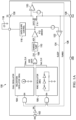
- FIG. 1A illustrates an example load switch circuit 100 to control power delivery to a load from a power supply.
- the example load switch circuit 100 includes an enable or "on" signal input 102 which, in turn, enables dual oscillators 104, 106 to generate clock input 108 for a charge pump 110.
- a first oscillator 104 is a relaxation oscillator (e.g., 10kHz, etc.) providing a slow clock signal that is XORed with a fast clock signal generated by the second oscillator 106 implemented as a ring oscillator (e.g., 2MHz, etc.) to provide the clock signal 108 to the charge pump 110.
- a relaxation oscillator e.g. 10kHz, etc.
- a fast clock signal generated by the second oscillator 106 implemented as a ring oscillator (e.g., 2MHz, etc.) to provide the clock signal 108 to the charge pump 110.
- the charge pump 110 is a power source for a gate driver 112, providing a charge pump voltage, V CP , to driver 112, which can then provide power to a gate 114.
- the driver 112 turns on the load switch 100 with the charge pump 110 to reduce on-resistance.
- a resistive driver 112 can provide smaller area, fast turn-on time, and zero IQ, for example.
- a gate slope control 116 can modify power-up of the gate 114 using an external capacitor 118 to control an in-rush current for soft start-up. Depending on the gate slope control 116, the driver 112 can deliver a fast main switch turn-on from the charge pump 110 in turbo mode.
- a state-of-charge (SOC) detector 122 turns off the oscillator(s) 104, 106 and charge pump 110 with a sleep signal 124 once the gate 114 turns on completely for low power.
- a comparator 120 can generate a turbo signal 126 to boost charging of VOUT 128 to VIN 130.
- the turbo comparator 120 detects when VOUT is smaller than VIN - offset voltage and trips the turbo signal 126 high which enables the ring oscillator 106 (e.g., fast frequency such as 2MHz, etc.).
- a high frequency clock 108 makes the charge pump 110 stronger to support a large driver current for a fast VOUT 128 turn-on feature with a small capacitor CT 118.
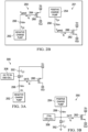
- FIG. 1B illustrates a timing diagram 150 for the example circuit 100 of FIG. 1A .
- the on signal 102 activates the circuit 100 to elevate VOUT 128 to VIN 130.
- VIN 130 powers the reference current IREF and the capacitor CT 118 to generate a controlled voltage slope.
- the turbo signal 126 is used to run the clock 108 faster by enabling the 2MHz ring oscillator 106 to support a large driver current that loads the charge pump 110 when VOUT is lower than VIN, for example.
- the sleep signal 124 is activated (e.g., trips low), allowing the circuit 100 to operate in low power mode.
- FIGS. 2A and 2B illustrate a comparison between different implementations of the driver 112 of the example of FIG. 1A , which are: a pair of current mirror drivers ( FIG. 2A ); and a pair of resistive drivers ( FIG. 2B ).
- FIG. 2A shows an example current mirror driver circuit 200, 201 shown with both a negative charge pump 202 for a P-channel FET-based circuit 200 and a positive charge pump 204 for an N-channel FET-based circuit 201.
- a positive charge pump 202 and negative charge pump 204 would not be used together with the same transistor, they represent complementary implementations to be used with the driver 112 depending on the type of transistor (e.g., the negative charge pump 202 for a P-channel FET 200 and the positive charge pump 204 for an N-channel FET 201, etc.) used to implement the driver 112.
- reference current sources 206 and 208 each provide a reference current, I REF .
- the current at transistor circuit 210, 212 is mirrored at transistor circuit 214, 216, to generate a gate current, Ig, corresponding to the I REF current source 206, 208, for example.
- the gate current, Ig is generated at a ratio of 1 to N (e.g., a current mirror ratio of 1:N) since a width of the transistor device 214, 216 is N times larger than a width of the transistor device 210, 212.
- the charge pumps 202, 204 work with the reference current sources 206, 208 and transistors 210-216 to create a gate current, Ig, that mirrors the reference current, I REF , sources 206, 208 to enable the load switch via a gate 218, 220.
- the switch is disabled and can be enabled by applying Ig to the gate 218, 220.
- Ig When Ig is supplied to the gate 218, 220, the gate 218, 220 is turned “on", which turns on the load switch.
- the gate 218, 220 When the gate 218, 220 is on, current flows through an associated transistor device (e.g., a power-FET, etc.) 222, 224 from source to drain, which provides electricity from a power source (VIN) to a connected load such as an electronic device (VOUT).
- the value of Ig determines how quickly or how slowly the switch 200, 201 turns on (is enabled). For example, the smaller the Ig, the slower the switch turns on, which produces less inrush current.
- drain-extended p-type metal-oxide-semiconductor (PMOS) logic can be used to pull up the gate 218 to disable the PMOS switch
- drain-extended n-type metal-oxide-semiconductor (NMOS) logic can be used to pull down the gate 220 to disable the NMOS switch.
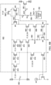
- FIG. 2B shows a pair of example resistive driver circuits 250, 251 including a P-channel FET circuit 250 with a negative charge pump 252 and an N-channel FET circuit 251 with a positive charge pump 254. While both a positive charge pump 252 and negative charge pump 254 would not be used together with the same transistor, they represent complementary implementations to be used with the driver 112 depending on the type of transistor (e.g., the negative charge pump 252 for a P-channel FET and the positive charge pump 254 for an N-channel FET, etc.) used to implement the driver 112.
- the negative charge pump 252 for a P-channel FET and the positive charge pump 254 for an N-channel FET, etc. used to implement the driver 112.
- the resistive drivers 250, 251 include a driver resistor, Rdrv, 256, 258 associated with the negative charge pump 252 and positive charge pump 254, respectively, and attached to a gate 260, 262.
- the charge pumps 252, 254 work with the resistors Rdrv 256, 258 to create a gate current, Ig, to enable the load switch via the gate 260, 262.
- the resistive driver 250, 251 occupies a smaller circuit footprint than the current mirror driver 200, 201, provides faster turn-on than the current mirror driver 200, 201, has lower I Q than the current mirror driver 200, 201, costs less to produce than the current mirror driver 200, 201, etc.
- no reference current, I REF is provided to the charge pump 252, 254, and, therefore, extra quiescent current introduced by the reference current is avoided.
- the resistive driver 250, 251 does not require an isolated drain-extended device to disable the load switch, which is not available in low-cost processes and is required by the current mirror implementation of FIG. 2A .
- the resistive driver 250, 251 provides a current that is not constant.
- the varying current in the resistive driver 250, 251 results in an inrush current applied to the switch when the switch is turned on that is also not constant.
- a varying or unpredictable inrush current can damage the switch when the inrush current is greater than a current capacity or threshold for which the switch was designed.
- a load-switch gate slope and a VOUT slope associated with the resistive driver circuit 250, 251 can also be variable (not constant).
- the load-switch gate slope is a rate of change in gate voltage, Vgate(t), over time. The gate slope depends on driver resistance, gate capacitance, input voltage, and charge pump voltage, for example.
- Gate slope can change exponentially based on driver resistance and gate capacitance, for example.
- the VOUT slope is a rate of change in output voltage, VOUT, over time.
- NMOS load-switch VOUT slope is equal to gate slope, and PMOS load-switch VOUT slope depends on a transconductance, g m (describing a ratio between output current and input voltage of the load switch), output resistance, driver resistance, gate capacitance, input voltage, and charge pump voltage, for example.
- Inrush current peak (e.g., a maximum value of the inrush current) varies with charge pump 252, 254 voltage, V CP , and variation in the driver resistor, Rdrv, 256, 258, so the inrush current is difficult to control.
- An unstable or unpredictable inrush current can be difficult to protect circuitry against, potentially resulting in damage to connected circuit components, for example.
- Inrush current flows from an input power supply (VIN) through a transistor 264, 266 (e.g., power-FET transistor, etc.) channel to an attached electronic device (VOUT).
- the inrush current is problematic because the power supply (VIN), connected transistor 264, 266, connected electronic device(s) (VOUT), and the circuit path between VIN and VOUT (the power path) are designed for a particular current capability. Therefore, an inrush current larger than the current capability for which circuitry is designed can damage that circuitry. Also, the inrush current can cause a decrease or "sag" in the power supply voltage, VIN, which provides power to other sub-systems as well. This power supply sag can trigger a system reset, for example.
- Ig t V CP ⁇ Vgate t Rdrv
- a direct current external capacitor, CT, 302 can be attached to the gate 260 and an electrostatic discharge (ESD) cell 306, which is a protection circuit that protects the device from electrostatic discharge, can be connected as well.
- ESD electrostatic discharge
- the external capacitor 302 at the gate 260 can be used for rise time control of a current mirror load driver switch.
- the presence of the external capacitor CT 302 results in an exponential change in gate slope (e.g., the gate slope is then based on Rdrv(C G + C CT ) time constant, where C G is a capacitance associated with the gate 260 and C CT is a capacitance associated with the capacitor 302) and high quiescent current (e.g., due to leakage current generated by the ESD cell 306) such that a high voltage rating external capacitor is required.
- the gate 260 discharges exponentially with a Rdrv(C G + C CT ) time constant.
- Ig(t) can be defined as in Equation 2
- Equation 3 peak inrush current varies with input supply voltage and Rdrv variation. This is important because a customer uses the single external capacitor CT 302 to prevent a large inrush current in multiple input supply voltage conditions. Also, the wide voltage range (e.g., -VIN to VIN) ESD device 306 creates a leakage current to the load-switch gate 260, and its effect is multiplied by the charge pump 252 gain, so I Q is increased. That is, the circuit of FIG. 3A produces a higher quiescent current due to the leakage current generated by the -VIN to VIN ESD cell 306. The ESD cell 306 can be large and have a wide width, thereby producing a leakage current that is not negligible.
- the wide voltage range e.g., -VIN to VIN
- the leakage current charges the gate 260, and the SOC detector 122 detects the charge on the gate 260.
- the detector 122 wakes the device 100 from sleep mode 124 to run the oscillator 104, 106, charge pump 110, and driver 112 to discharge the charge formed by the leakage current from the ESD cell 306.
- the leakage current from the ESD cell 306 wakes up the device 100 more frequently and increases quiescent current.
- quiescent current is not impacted by an ESD cell leakage current, resulting in a lower quiescent current, for example.
- the example NMOS load switch 350 includes an external capacitor CT 352, attached to the gate 262 and wide voltage range (e.g., 0V to 2*VIN) ESD cell 356.
- the resistor Rdrv 258 is also attached between the positive charge pump 254 and the gate 262.
- FIG. 4 illustrates an example NMOS constant gate slope control and driver circuit 400 with driver cancellation current, Ict.
- the example circuit 400 includes the positive charge pump 254, the driver resistor, Rdrv, 258, the gate 262, a V to I transconductor 408 to convert a voltage to a current, a capacitor, CT, 352, and a reference current, I REF , source 412.
- the charge pump 254 and driver resistor 258 form and/or replace the charge pump 110/driver 112 combination shown in FIG. 1A
- the transconductor 408, capacitor 352, and reference current source 412 form and/or replace the gate slope control 116/capacitor 118 combination shown in FIG. 1A , for example.
- Ict from the capacitor 352 and transconductor 408 helps to stabilize a driver current, Idrv, to provide a constant slope for change in gate 262 voltage (e.g., a constant gate slope), and the transconductor 408 provides separation between the capacitor 352 and the gate 262 to avoid or reduce leakage current, for example.
- Idrv driver current
- the transconductor 408 provides separation between the capacitor 352 and the gate 262 to avoid or reduce leakage current, for example.
- the driver current, Idrv flows through the resistor 258, and a gate current, Ig, flows to the gate 262.
- a capacitor 352 voltage, V CT is converted to a capacitor current, Ict, by the transconductor 408 with a gain of 2/Rdrv.
- a time constant associated with the Ict is larger than a time constant associated with Idrv (e.g., for a large CT 352).
- Equation 14 representing a gate slope for the example circuit 400 of FIG. 4
- Equation 3 representing a gate slope for the example circuit 300 of FIG. 3A
- the example circuit 400 provides a constant gate slope as represented in Equation 14.
- Ict 2*Vct/Rdrv
- Idrv approximately follows Ict.
- Gate Slope 2*Cct/I REF , for example.
- FIG. 5B shows an example magnification of the relationship between Ict and Idrv, with Idrv approximating the slope of Ict.
- N-channel N-channel
- PCH P-channel
- the V to I transconductor gain (1+N)/Rdrv.
- FIG. 6A illustrates a schematic view of an example constant gate slope control and driver circuit 600 including a transconductor 602 to control the gate 260 with the charge pump 252, the resistive driver 256, and an ESD cell 610.
- the transconductor 602 separates the ESD cell 610 from the gate 260 to reduce or avoid leakage current effects.
- the example circuit 600 can be implemented as a chip to provide power to another device, circuit, chip, etc., and/or as part of a system-on-a-chip to provide and regulate power to other parts of the chip, etc.
- FIG. 6B illustrates a schematic view of the example circuit 600 showing component implementation detail for the example transconductor 602 with respect to the charge pump 252 and the gate 260.
- the transductor 602 can be implemented using a plurality of transistors 620-630 (e.g., MOSFETs, other FETs, etc.), including natural N-channel (NCH) transistors (e.g., MOSFETs, etc.) 624-630, and resistors 640, 642 having a quarter of the resistance value of the resistive driver 256 (e.g., Rdrv/4).
- transistors 620-630 e.g., MOSFETs, other FETs, etc.
- NCH natural N-channel transistors
- resistors 640, 642 having a quarter of the resistance value of the resistive driver 256 (e.g., Rdrv/4).
- Each natural or native N-channel transistor 624-630 is a transistor (e.g., a MOSFET) that operates in an intermediate mode between enhancement and depletion modes.
- a natural N-channel MOSFET includes a natural thin oxide film formed over silicon during processing of other layers and has nearly zero threshold voltage, functioning as a weak pull-down in low-voltage applications, etc.
- an enhancement mode MOSFET increases device conductivity when a voltage is applied to the gate and a depletion mode MOSFET reduces conductivity based on a voltage applied to the gate
- a natural or native MOSFET has nearly zero threshold voltage and provide a weak pull-down for low-voltage applications where enhancement mode or depletion mode MOSFETs may be too strong.
- native mode MOSFETs can enable a load switch for low voltage electronic devices using low current and low voltage to avoid leakage and quiescent current effects, etc.
- the current Ict flowing through the transconductor 602 slows down a gate discharge speed through its interaction with the driver current to provide a constant gate slope control, for example.
- Benefits of constant gate slope control include little ESD 610 leakage current loading to the negative charge pump 252, resulting in minimal I Q , for example.
- the (0 to VIN) ESD cell 610 can also be implemented as a low-area cell on a low-cost die, for example.
- a linearly discharged gate also provides a better-controlled inrush current by reducing or eliminating fluctuations and/or other variability in gate voltage, for example. Further, changes enabled in capacitor CT pin rating (e.g., from -VIN ⁇ VIN to 0V ⁇ VIN) reduce system cost.
- FIG. 7A illustrates a zero-I Q implementation of an example NMOS load switch 700 with constant gate slope control according to the invention.
- the example circuit 700 includes shut-off circuitry to shut off the gate slope control circuitry when not needed so that zero quiescent current is produced. More specifically, the example circuit 700 includes a comparator 702, which compares V CT to ground or close to ground (e.g., within 50mV, etc.) to determine when gate 262 voltage has reached maximum charge pump 254 voltage.
- V CT voltage
- the V CT to 50mV comparator 702 detects this condition and triggers a shut-off signal 704, which can be stored in a latch, flip-flop, or register 706, to shut off, deactivate, and/or otherwise disable gate slope control circuitry including the capacitor 352 and the transconductor 408, to make a zero quiescent current.
- V CT is also pulled up to VIN to prepare for a next soft-start, for example.
- FIG. 7B illustrates an example timing diagram 708 reflecting activation of the example circuit 700 and its shut-off signal 704.
- V CT begins to decrease from VIN as the capacitor discharges.
- Gate 262 voltage is correspondingly increasing as current is applied to the gate 262, as is output voltage VOUT.
- the comparator 702 triggers the shut-off signal 704, which initiates a period of zero I Q because the circuit 700 is in steady state at maximum charge pump 254 voltage.
- V CT is increased back to VIN.
- VOUT and gate voltage decrease to ground.
- V CT again decreases to ground as gate voltage and VOUT increase to steady state.
- FIG. 7C depicts an example NMOS transistor implementation of cancellation current circuitry in the transconductor 408 of the circuit 700 for NMOS constant gate slope control through generation of cancellation current Ict.
- the cancellation current Ict correlates with the driver current Idrv and the gate current Ig with respect to the gate 262, charge pump 254, and resistor Rdrv 258, for example.
- An input voltage VIN and the capacitor CT 352 are connected via a plurality of transistors and resistors to generate and relay the current Ict, when enabled, with respect to a reference current I REF , for example.
- a plurality of transistor gates 722-742 including NMOS transistors MN1 740 and MN2 742, and resistors 746, 748 relay current Ict from the capacitor CT 352 to the gate 262.
- FIG. 7D depicts an example NMOS transistor implementation of shut-down detection circuitry, such as the comparator 702, generating the shut-off output signal 704 (represented as disable signals CT_D 704 and CT_DZ 710 in the example of FIG. 7D ) to be stored in and provided by the S-R latch 706 and sent to gates of the transconductor circuit 408, capacitor 352, and comparator 702 to temporarily turn off or disable those components.
- the circuitry 352 ,408, 702 quiescent current I Q can be reduced to zero, resulting in no leakage of current from the circuit 700 to connected component(s). As shown in the example of FIG.
- a CT DZ EN enable or disable signal 716 can be formed by ANDing disable signal CT_DZ 710 and enable signal EN 712.
- a completion signal CT_done 750 can indicate when VCT is approximately ground, and the shut-off signal(s) 704, 710 are to be provided by the latch 706, for example.
- FIGS. 8A-8C depict example PMOS circuitry 800 corresponding to the NMOS circuitry 700 of FIGS. 7A-7D , with a negative charge pump 252 rather than a positive charge pump 254 to provide constant gate slope control to regulate gate voltage during activation using the capacitor 302 and transconductor 602 and help ensure zero to low quiescent current through shut-off circuitry once the gate 260 has been turned on.
- FIG. 8A depicts an example a zero-to implementation of an example PMOS load switch 800 with constant gate slope control according to the invention.
- a shut-off signal 802 can be generated using a comparator 804.
- the comparator 804 of the example circuit 800 compares V CT to ground or close to ground (e.g., within 50mV, etc.) to determine when gate 260 voltage has reached maximum charge pump 252 voltage (e.g., is turned on or activated, which corresponding turns on the load switch to provide an output voltage to a connected electronic device).
- V CT voltage
- the V CT to 50mV comparator 804 detects this condition and triggers a shut-off signal 802, which can be stored in a latch, flip-flop, or register 806, to shut off, deactivate, and/or otherwise disable gate slope control circuitry including the capacitor 302 and the transconductor 602, to make a zero quiescent current.
- V CT is also pulled up to VIN to prepare for a next soft-start, for example.
- FIG. 8B shows an example PMOS transistor implementation of cancellation current generation circuit implementing the transconductor circuit 602.
- the cancellation current Ict correlates with the driver current Idrv and the gate current Ig with respect to the gate 260, charge pump 252, and resistor Rdrv 256, for example.
- An input voltage VIN and the capacitor CT 302 are connected via a plurality of transistors and resistors to generate and relay the current Ict, when enabled, with respect to a reference current I REF , for example.
- a plurality of transistor gates 820-846 including NMOS transistors MN1 834 and MN2 836 and PMOS transistors MP1 842 and MP2 844, and resistors 850, 852 relay current Ict from the capacitor CT 302 to the gate 260.
- FIG. 8C depicts an example PMOS transistor implementation of shut-down detection circuitry, such as the comparator 804, generating the shut-off output signal 802 (represented as disable signals CT_D 802 and CT_DZ 810 in the example of FIG. 8C ) to be stored in and provided by the S-R latch 806 sent to gates of the transconductor circuit 602, capacitor 302, and comparator 804 to temporarily turn off or disable those components.
- the circuitry 302, 602, 804 quiescent current I Q can be reduced to zero, resulting in no leakage of current from the circuit 800 to connected component(s). As shown in the example of FIG.
- a CT_DZ_EN enable or disable signal 816 can be formed by ANDing disable signal CT_DZ 810 and enable signal EN 812.
- a completion signal CT_done 854 can indicate when V CT is approximately ground, and the shut-off signal(s) 802, 810 are to be provided by the latch 806, for example.
- FIG. 9A illustrates an example 4-pin very thin small outline no lead (WSON) package 900 shown in a laser marking view providing contacts for ON 902, ground 904, input voltage VIN 906, and output voltage VOUT 908 to implement a load switch.
- a power supply can be connected to the input voltage contact 906, and an electronic device to be powered can be connected to the output voltage contact 908, for example.
- the example package 900 can be used to provide a power FET in a wafer-level chip-scale package (WCSP) using the load switch circuit described herein to regulate power to another device such as a haptic driver, biosensor, light sensor, converter, regulator, etc.
- WCSP wafer-level chip-scale package
- Such a FET can handle high power levels while also providing good efficiency at low voltages and with high commutation speed.
- FIG. 9B illustrates an example 6-pin small outline transistor (SOT-23) package 950 to house load switch circuitry 100-800 shown in a top view including pins for VIN 952, VOUT 954, ground GND 956, quick output discharge (QOD) 958, ON 960, and external capacitor CT connection 962 to implement a load switch.
- the example package 950 can also be used to provide a power FET using the load switch circuit described herein to regulate power to another device such as an active antenna system, remote radio unit, set top box, digital video recorder, etc.
- a charge pump can be included in the package 900, 950 and/or provided as an external charge pump to be connected via an additional package pin (not shown) to the resistive driver (Rdrv) in the load-switch circuitry of the package 900, 950.
- the charge pump can be eliminated from a PMOS load switch. Instead, the resistive driver can be connected to ground and the gate of the PMOS load switch, and the transconductor gain, K, can be 1/Rdrv, for example.
- the charge pump is used to turn on the NMOS load switch.
- Certain examples provide a constant load-switch gate slope control and driver with a novel external capacitor time constant-based driver cancellation current for a resistive driver load-switch that enables a wide range turn-on time with a small area.
- Certain examples provide digital loop circuitry that detects when gate slope control is completed and shuts off circuitry to make zero quiescent current. The digital loop circuit also pulls up capacitor voltage to input voltage (VIN) for a next rise time control.
- Certain examples provide technical advantages through a wide range of turn-on times including fast with no external capacitor and slow with a large capacitor.
- Certain examples generate no quiescent current using a shut-down or shut-off technique once gate slope control is complete.
- inrush current does not vary with supply voltage and poly resistor variation.
- the driver and gate slope control can be provided in a small footprint, and a voltage rating of the external capacitor can be reduced (e.g., based on a number of charge pump stages included in the circuit) over a traditional external capacitor.
- Certain examples improve upon prior current mirror driver circuit designs by providing a resistive gate driver circuit including a transconductor and comparator to facilitate load switch gate driving, gate slope control, and shut-off once gate slope control is complete.
- circuitry e.g., the transconductor, comparator, etc.
- circuitry can be implemented using N-type metal-oxide-semiconductor logic components or P-type metal-oxide-semiconductor logic components.
- Implementing the load switch circuit as an NMOS load switch with a positive charge pump or as a PMOS load switch with a negative charge pump has different advantages and disadvantages.
- implementing an NMOS load-switch with a positive charge pump provides advantages including that VOUT follows GATE since the NMOS load-switch is acting as source follower amplifier.
- constant gate slope corresponds to a constant VOUT slope.
- the NMOS load-switch is smaller than the equivalent PMOS load-switch, for example.
- the NMOS load-switch allows a higher leakage current than the PMOS load-switch when the load switch is turned off.
- the PMOS load switch can be turned on at low VIN (e.g., 1V) with a single stage charge pump.
- VIN e.g. 1V
- VIN 1V
Description
- This relates generally to power regulators, and more particularly to a low quiescent current load switch.
- Power management integrated circuits (ICs) can be used to drive circuits in applications ranging from automotive to communications and industrial technologies. Power switches are commonly used to couple a power supply to a device such as a digital logic circuit or a memory cell. Load switches, such as integrated load switches, are IC relays used to turn on and off power rails. A basic load switch includes four connections: input voltage, output voltage, enable, and ground. An IC version of a load switch provides a smaller footprint than a load switch formed from discrete components. An IC load switch can be formed using a complementary metal-oxide-semiconductor (CMOS) process to include an output transistor and an output driver, for example. A load switch can be used in a system to improve power consumption by reducing current leakage, for example. When the load switch is turned on, current is allowed to flow from the input pin to the output pin, and power is passed to downstream circuitry.
- An example of a load switch circuit according to the preamble of
claim 1 is known fromCN 107 508 462 A . - A load switch circuit according to the invention is defined in appended independent claim 1.Further preferred embodiments are defined in dependent claims 2-5.
-
-
FIG. 1A illustrates an example load switch circuit to control power delivery to a load from a power supply. -
FIG. 1B illustrates a timing diagram for the example circuit ofFIG. 1A . -
FIG. 2A illustrates an example current mirror driver implementation of the driver ofFIG. 1A . -
FIG. 2B illustrates an example resistive driver implementation of the driver ofFIG. 1A . -
FIG. 3A illustrates an example PMOS load switch. -
FIG. 3B illustrates an example NMOS load switch. -
FIG. 4 illustrates an example NMOS constant gate slope control and driver circuit. -
FIGS. 5A-5B show an example timing diagram for the circuit ofFIG. 4 . -
FIGS. 6A-6B illustrate an example constant gate slope control and driver circuit for a PMOS load switch. -
FIG. 7A illustrates a zero quiescent current implementation of an example NMOS load switch with constant gate slope control according to the invention. -
FIG. 7B depicts an example timing diagram associated with operation of the circuit ofFIG. 7A . -
FIG. 7C depicts an example NMOS transistor implementation of cancellation current circuitry for the load switch ofFIG. 7A . -
FIG. 7D depicts an example NMOS transistor implementation of shut-down detection circuitry for the load switch ofFIG. 7A . -
FIG. 8A illustrates a zero quiescent current implementation of an example PMOS load switch with constant gate slope control. control according to the invention. -
FIG. 8B depicts an example PMOS transistor implementation of cancellation current circuitry for the load switch ofFIG. 8A . -
FIG. 8C depicts an example PMOS transistor implementation of shut-down detection circuitry for the load switch ofFIG. 8A . -
FIGS. 9A-9B illustrate example device packages including circuitry to implement a load switch. - The drawings are not to scale. Wherever possible, the same reference numbers are used throughout the drawing(s) and accompanying written description to refer to the same or like parts.
- Logical, mechanical, electrical and/or other changes may be made without departing from the scope of the subject matter of this description. Certain features from different aspects of this description may be combined to form additional aspects of the subject matter described below.
- Integrated load switches are electronic relays that can be used to turn on and turn off power supply rails in electrical systems. Load switches offer many benefits to an electrical system and can include protection features that are often difficult to implement with discrete components. For example, load switches can be used to regulate power distribution, power sequencing/power state transition, inrush current control, reduced leakage current in standby mode, controller power down, etc. Pass transistor logic, such as a pass field-effect transistor (FET), is activated (e.g., "turns ON") when the load switch device is enabled via its "ON" pin. Activation allows current to flow from an input pin to an output pin and power to pass to downstream circuitry connected to the switch.
- The pass FET of the load switch determines a maximum input voltage and a maximum load current that the load switch can handle. An on-resistance of the load switch is a characteristic of the pass FET that can be used in calculating power dissipated by the load switch. The pass FET can be either an N-channel or P-channel FET, which will determine the architecture of the load switch. A gate driver charges and discharges the gate of the FET in a controlled manner, thereby controlling a voltage supply rise time of a device connected to the load switch. Control logic for the load switch is driven by an external logic signal. The control logic controls the turn-on and turn-off of the pass FET and other blocks, such as quick output discharge, a charge pump, and blocks with protection features.
- A charge pump circuit uses capacitors and/or other storage elements to convert and, optionally, regulate voltage to generate an output voltage that can be higher or lower than the charge pump input voltage. A charge pump may not be included in a load switch but, if present, the charge pump can be used in load switches with a FET (e.g., a positive charge pump with an N-channel FET or a negative charge pump with a P-channel FET) because a positive differential voltage between the gate and the source (VOUT) is needed to turn on the FET properly.
- A load switch can include a quick output discharge utilizing an on-chip resistor between VOUT and ground (GND). The resistor can be activated (e.g., turned on) when the load switch device is disabled via the ON pin. Activation will discharge the output node, thereby preventing the output from floating at an unpredictable voltage. Quick output discharge can be available to a load switch device when an input voltage (VIN) and a bias voltage (VBIAS) are within an operating range.
- For example, many systems have limited control of sub-system power distribution. Load switches can be used to turn on and off sub-systems of the same input voltage rather than using multiple direct current (DC)/DC converters or low-dropout (LDO) regulators. By using a load switch, power can be distributed across different loads with control for each individual load.
- In some systems, such as systems including a processor, there is a strict power-up sequence to be followed. By using a general-purpose input/output (GPIO) or inter-integrated circuit (I2C) interface, load switches can implement power sequencing to meet power-up requirements. Load switches can provide independent control of each power path to provide simplified point-of-load control for power sequencing.
- In certain examples, some sub-systems are only used during certain modes of operation. Load switches can be used to limit an amount of leakage current and power consumption by turning off power to these sub-systems. In some applications, the circuitry, such as DC/DC converters, LDOs, modules, etc., can be disabled and put into standby mode. However, the leakage current of these modules can be relatively high, even in the shutdown state. By placing a load switch before the load, the leakage can be reduced to significantly lower levels. Thus, power consumption can be reduced significantly with a load switch placed in the power path.
- An inrush current (also referred to as an input surge current or switch-on surge) is an instantaneous input current drawn by an electrical device when the device is turned on and can be several times larger than a normal operating current for a few cycles before reducing to normal current levels. Because the inrush current is sudden and larger than a normal operating current for the circuit, the inrush current can damage connected transistor devices (e.g., a FET such as a Power-FET, etc.), power path circuitry through which the input power flows, and/or other connected circuit, etc.
- In certain examples, when turning on a sub-system without any voltage supply slew rate control, a voltage supply rail can sag (e.g., dip or temporarily decrease) due to an inrush current that can happen from quickly charging capacitance. The sagging voltage supply rail can be problematic as this rail may be supplying power to other sub-systems. Load switches solve this issue by controlling the rise time of the output voltage, thereby eliminating the sag on the input voltage.
- In certain examples, when a DC/DC converter or LDO without quick output discharge turns off, the load voltage is left floating and power down is dictated by the load. This can cause unwanted activity as modules downstream are not powered down to a defined state. Using a load switch with quick output discharge can mitigate these problems. The load can be powered down quickly in a controlled manner and reset to a known good state for the next power up. The quick, controlled power down and reset can eliminate floating voltages at the load and help ensure that the device is in a defined power state.
- Certain applications can include fault protection features to be integrated into the load switch. Some load switches include integrated features such as reverse current protection, ON pin hysteresis, current limiting, undervoltage lock-out and over temperature protection, etc. Rather than implementing these complex circuits through discrete components, part count, solution size, and development time can be reduced using an integrated load switch.
- Protection features can include reverse current protection to stop current from flowing from the VOUT pin to the VIN pin. In the absence of this feature, current may flow from the VOUT pin to the VIN pin, if the voltage on VOUT is greater than VIN by a diode drop. Thus, reverse current blocking can be beneficial in certain applications, such as in a power mux application, where current should not flow from VOUT to VIN.
- Protection can also include reverse current protection. There are many different methods of implementing reverse current protection. In some example, the device monitors the voltage levels at the VIN pin and VOUT pin. When this differential voltage exceeds a certain threshold, the switch is disabled, and the body diode is disengaged to prevent any reverse current flow to VIN. Some devices have reverse current protection when the device is disabled.
- In some example, ON pin hysteresis allows for more robust GPIO enable. With a voltage difference between a logic level high and logic level low on the ON pin, control circuitry operates as intended when there is noise on the GPIO line.
- In certain examples, over temperature protection disables the switch if the temperature of the device exceeds a threshold temperature. With this feature, the device can operate as a safety switch that turns off when a high temperature is detected.
- Using an integrated load switch can lower the part count of a system. If there are discrete FETs that are used in conjunction with other components, a load switch could be considered to reduce the number of total components in the system. When a load switch is created discretely, there are many resistors, capacitors and transistors required to implement a gate driver, control logic, output discharge and protection features. With an integrated load switch, this is accomplished with a single device, and the part count is significantly reduced.
- Quiescent current (IQ) is a small current that flows when the load switch device is in an inactive state (e.g., idle, asleep, off, etc.). For example, a device that is turned on but in a minimal or reduced state (e.g., an amplifier IC that is on and ready to operate (e.g., enabled) but is not currently amplifying anything, etc.) consumes IQ. For example, quiescent current is the current drawn when the load switch device is enabled and there is no load on the output. The IQ is a result of the power needed for the many different parts of the load switch, such as charge pump, gate driver, control logic, etc. That is, the load switch can include a quiescent current to provide a low on-resistance (RON) across input voltages. Quiescent current dictates minimum power consumption of a circuit, maximum battery life of a device, etc.
- In certain examples involving load switches, the quiescent current passes through the device to the ground connection, rather than through the pass FET. A quiescent current for a load switch is usually in the microamp (µA) range, for example. In such examples, for an output load in milliamps (mA) or higher, such as an LED, the quiescent current becomes a negligible percentage because the quiescent current is small compared to the current needed to power the entire system. However, the quiescent current is not negligible while the load switch is disabled/off.
- Certain examples described herein provide a low quiescent current, low-cost switch mode power regulator load switch. Certain examples described herein provide an associated zero-IQ, low cost external capacitor-based constant gate slope control method for a load switch powering electronics. While some approaches utilize a current mirror driver, for fast rise time, low quiescent current, and small area, as described herein, a gate driver can be a resistive driver instead of a current mirror driver. Certain examples employ a resistive gate driver to facilitate zero-IQ, constant gate slope load switch control with capacitor current decreasing at the same rate as capacitor voltage (e.g., same slope of decrease or discharge) to provide a stable, low quiescent current to control the load switch without current leakage.
-
FIG. 1A illustrates an exampleload switch circuit 100 to control power delivery to a load from a power supply. The exampleload switch circuit 100 includes an enable or "on"signal input 102 which, in turn, enablesdual oscillators clock input 108 for acharge pump 110. In the example ofFIG. 1A , afirst oscillator 104 is a relaxation oscillator (e.g., 10kHz, etc.) providing a slow clock signal that is XORed with a fast clock signal generated by thesecond oscillator 106 implemented as a ring oscillator (e.g., 2MHz, etc.) to provide theclock signal 108 to thecharge pump 110. - The
charge pump 110 is a power source for agate driver 112, providing a charge pump voltage, VCP, todriver 112, which can then provide power to agate 114. Thedriver 112 turns on theload switch 100 with thecharge pump 110 to reduce on-resistance. Aresistive driver 112 can provide smaller area, fast turn-on time, and zero IQ, for example. Agate slope control 116 can modify power-up of thegate 114 using anexternal capacitor 118 to control an in-rush current for soft start-up. Depending on thegate slope control 116, thedriver 112 can deliver a fast main switch turn-on from thecharge pump 110 in turbo mode. A state-of-charge (SOC)detector 122 turns off the oscillator(s) 104, 106 andcharge pump 110 with asleep signal 124 once thegate 114 turns on completely for low power. Once thegate 114 is activated, acomparator 120 can generate aturbo signal 126 to boost charging ofVOUT 128 toVIN 130. Theturbo comparator 120 detects when VOUT is smaller than VIN - offset voltage and trips theturbo signal 126 high which enables the ring oscillator 106 (e.g., fast frequency such as 2MHz, etc.). Ahigh frequency clock 108 makes thecharge pump 110 stronger to support a large driver current for afast VOUT 128 turn-on feature with asmall capacitor CT 118. -
FIG. 1B illustrates a timing diagram 150 for theexample circuit 100 ofFIG. 1A . As shown in the example diagram 150, the onsignal 102 activates thecircuit 100 to elevateVOUT 128 toVIN 130. Thecapacitor CT 118 charges with a constant reference current IREF which makes a constant CT voltage slope = Cct/IREF, where Cct is a capacitance value of the capacitor CT. In certain examples,VIN 130 powers the reference current IREF and thecapacitor CT 118 to generate a controlled voltage slope. Theturbo signal 126 is used to run theclock 108 faster by enabling the2MHz ring oscillator 106 to support a large driver current that loads thecharge pump 110 when VOUT is lower than VIN, for example. When the main switch is powered on, as verified by theSOC detector 122, thesleep signal 124 is activated (e.g., trips low), allowing thecircuit 100 to operate in low power mode. -
FIGS. 2A and2B illustrate a comparison between different implementations of thedriver 112 of the example ofFIG. 1A , which are: a pair of current mirror drivers (FIG. 2A ); and a pair of resistive drivers (FIG. 2B ).FIG. 2A shows an example currentmirror driver circuit negative charge pump 202 for a P-channel FET-basedcircuit 200 and apositive charge pump 204 for an N-channel FET-basedcircuit 201. While both apositive charge pump 202 andnegative charge pump 204 would not be used together with the same transistor, they represent complementary implementations to be used with thedriver 112 depending on the type of transistor (e.g., thenegative charge pump 202 for a P-channel FET 200 and thepositive charge pump 204 for an N-channel FET 201, etc.) used to implement thedriver 112. In the example pair of currentmirror driver circuits current sources transistor circuit transistor circuit current source - As shown in the example of
FIG. 2A , the gate current, Ig, is generated at a ratio of 1 to N (e.g., a current mirror ratio of 1:N) since a width of thetransistor device transistor device 
FIG. 2A , the charge pumps 202, 204 work with the referencecurrent sources sources gate - As shown in the example of
FIG. 2A , the switch is disabled and can be enabled by applying Ig to thegate gate gate gate switch gate 218 to disable the PMOS switch, and drain-extended n-type metal-oxide-semiconductor (NMOS) logic can be used to pull down thegate 220 to disable the NMOS switch. -
FIG. 2B shows a pair of exampleresistive driver circuits channel FET circuit 250 with anegative charge pump 252 and an N-channel FET circuit 251 with apositive charge pump 254. While both apositive charge pump 252 andnegative charge pump 254 would not be used together with the same transistor, they represent complementary implementations to be used with thedriver 112 depending on the type of transistor (e.g., thenegative charge pump 252 for a P-channel FET and thepositive charge pump 254 for an N-channel FET, etc.) used to implement thedriver 112. Rather than the current mirror ofcircuits resistive drivers negative charge pump 252 andpositive charge pump 254, respectively, and attached to agate FIG. 2B , the charge pumps 252, 254 work with theresistors Rdrv gate - The
resistive driver current mirror driver current mirror driver current mirror driver current mirror driver resistive driver charge pump resistive driver FIG. 2A . - However, the
resistive driver resistive driver resistive driver circuit - An inrush current peak (e.g., a maximum value of the inrush current) varies with
charge pump transistor 264, 266 (e.g., power-FET transistor, etc.) channel to an attached electronic device (VOUT). The inrush current is problematic because the power supply (VIN), connectedtransistor - Gate current, Ig(t), can be calculated using a charge pump voltage, VCP, a gate voltage Vgate(t), and driver resistance, Rdrv, as:

circuit resistive driver circuit circuit - As shown in the example
PMOS load switch 300 ofFIG. 3A , a direct current external capacitor, CT, 302 can be attached to thegate 260 and an electrostatic discharge (ESD)cell 306, which is a protection circuit that protects the device from electrostatic discharge, can be connected as well. Theexternal capacitor 302 at thegate 260 can be used for rise time control of a current mirror load driver switch. However, in a resistive driver load switch with thedriver resistor Rdrv 256 coupled between thenegative charge pump 252 and thegate 260, the presence of theexternal capacitor CT 302 results in an exponential change in gate slope (e.g., the gate slope is then based on Rdrv(CG + CCT) time constant, where CG is a capacitance associated with thegate 260 and CCT is a capacitance associated with the capacitor 302) and high quiescent current (e.g., due to leakage current generated by the ESD cell 306) such that a high voltage rating external capacitor is required. - For example, the
gate 260 discharges exponentially with a Rdrv(CG + CCT) time constant. Ig(t) can be defined as inEquation 2, and a change ingate 260 voltage over time, referred to as gate slope, can be defined as:
- As shown in
Equation 3, peak inrush current varies with input supply voltage and Rdrv variation. This is important because a customer uses the singleexternal capacitor CT 302 to prevent a large inrush current in multiple input supply voltage conditions. Also, the wide voltage range (e.g., -VIN to VIN)ESD device 306 creates a leakage current to the load-switch gate 260, and its effect is multiplied by thecharge pump 252 gain, so IQ is increased. That is, the circuit ofFIG. 3A produces a higher quiescent current due to the leakage current generated by the -VIN toVIN ESD cell 306. TheESD cell 306 can be large and have a wide width, thereby producing a leakage current that is not negligible. The leakage current charges thegate 260, and theSOC detector 122 detects the charge on thegate 260. Thedetector 122 wakes thedevice 100 fromsleep mode 124 to run theoscillator charge pump 110, anddriver 112 to discharge the charge formed by the leakage current from theESD cell 306. Thus, the leakage current from theESD cell 306 wakes up thedevice 100 more frequently and increases quiescent current. As described further below, by isolating a capacitor, CT, to thegate 260, quiescent current is not impacted by an ESD cell leakage current, resulting in a lower quiescent current, for example. - Similar effects are exhibited in an
NMOS load switch 350 such as shown in the example ofFIG. 3B . The exampleNMOS load switch 350 includes anexternal capacitor CT 352, attached to thegate 262 and wide voltage range (e.g., 0V to 2*VIN)ESD cell 356. Theresistor Rdrv 258 is also attached between thepositive charge pump 254 and thegate 262. -
FIG. 4 illustrates an example NMOS constant gate slope control anddriver circuit 400 with driver cancellation current, Ict. Theexample circuit 400 includes thepositive charge pump 254, the driver resistor, Rdrv, 258, thegate 262, a V to I transconductor 408 to convert a voltage to a current, a capacitor, CT, 352, and a reference current, IREF,source 412. Thecharge pump 254 anddriver resistor 258 form and/or replace thecharge pump 110/driver 112 combination shown inFIG. 1A , and thetransconductor 408,capacitor 352, and referencecurrent source 412 form and/or replace thegate slope control 116/capacitor 118 combination shown inFIG. 1A , for example. The introduction of Ict from thecapacitor 352 andtransconductor 408 helps to stabilize a driver current, Idrv, to provide a constant slope for change ingate 262 voltage (e.g., a constant gate slope), and thetransconductor 408 provides separation between thecapacitor 352 and thegate 262 to avoid or reduce leakage current, for example. - As shown in the example of
FIG. 4 , the driver current, Idrv, flows through theresistor 258, and a gate current, Ig, flows to thegate 262. Using theexample circuit 400, acapacitor 352 voltage, VCT, is converted to a capacitor current, Ict, by thetransconductor 408 with a gain of 2/Rdrv. Initially, Ict and Idrv can be equal so that no current flows to the gate 262 (Ig = 0), but a slowly changing linear Ict (cancellation current) interacts with a fast-changing Idrv from theresistive driver 258 such that thegate 262 voltage has a linear (constant slope). In certain examples, a time constant associated with the Ict is larger than a time constant associated with Idrv (e.g., for a large CT 352). As a result, Idrv tracks Ict closely and becomes a constant slope for thegate 262, with a gate slope, dVgate/dt, with respect to apower supply 422 providing an input voltage VIN and anelectronic device 424 connected to an output voltage VOUT, constant at twice VCT slope, for example:
- In certain examples, a determination of NMOS load-switch constant gate slope can be calculated over time, t, for an input voltage, VIN, as follows:


example circuit 400 ofFIG. 4 , can be compared toEquation 3, representing a gate slope for theexample circuit 300 ofFIG. 3A . Rather than the exponential gate slope ofEquation 3, theexample circuit 400 provides a constant gate slope as represented in Equation 14. - As shown in the example timing diagram 500 of
FIG. 5A , when thecircuit 400 is activated or turned "on" 502, Vct begins to decrease from input voltage VIN with a slope of Vct Slope = Cct/IREF. After an initial ramp-up with power on 502 (Ict = 2*Vct/Rdrv), Ict similarly decreases with a slope of Ict Slope = 2*Cct/IREF., and Idrv approximately follows Ict. Gate current Ig stays relatively constant at Ig = Ict - Idrv, andgate 262 slope increases along with VOUT, which plateaus as Vct and Ict reach the end of their downward slope. Thus, Gate Slope = 2*Cct/IREF, for example.FIG. 5B shows an example magnification of the relationship between Ict and Idrv, with Idrv approximating the slope of Ict. - While the above equations are determined for a single-
stage charge pump 254, a number of stages can be used depending upon the circuit implementation. The equations can be extended for an N-stage charge pump 254 (e.g., 2-stage, 3-stage, etc.). Thus, more generally, for an N-stage charge pump 254, V to I transconductor 408 gain can be represented as: (1+N)/Rdrv. That is, with a single-stage charge pump 254 (e.g., positive charge pump Vcp = 2*VIN for an N-channel (NCH) load switch and negative charge pump Vcp = -VIN for a P-channel (PCH) load switch with initial gate to charge pump voltage difference = 2*VIN). If a two-stage charge pump 254 is used, the positive charge pump Vcp = 3*VIN for an NCH load switch and the negative charge pump Vcp = -2VIN for PCH load switch with an initial gate to charge pump voltage difference = 3*VIN. For such a two-stage charge pump 254, the current input is to be 3Vct/Rdrv (e.g., a transconductor gain of 3/Rdrv and resistors = Rdrv/3, etc.). Thus, given an N-stage charge pump, the V to I transconductor gain = (1+N)/Rdrv. Similarly, with an N-stage charge pump, gate slope, GATE(t), can be represented as: GATE(t) = dVgate/dt = (N+1)*IREF/CCT, where input voltage VIN powers the reference current IREF and the capacitor CT provides a capacitance CCT to generate a controlled voltage slope. -
FIG. 6A illustrates a schematic view of an example constant gate slope control anddriver circuit 600 including atransconductor 602 to control thegate 260 with thecharge pump 252, theresistive driver 256, and anESD cell 610. Thetransconductor 602 separates theESD cell 610 from thegate 260 to reduce or avoid leakage current effects. Theexample circuit 600 can be implemented as a chip to provide power to another device, circuit, chip, etc., and/or as part of a system-on-a-chip to provide and regulate power to other parts of the chip, etc. -
FIG. 6B illustrates a schematic view of theexample circuit 600 showing component implementation detail for theexample transconductor 602 with respect to thecharge pump 252 and thegate 260. As shown in the example ofFIG. 6B , thetransductor 602 can be implemented using a plurality of transistors 620-630 (e.g., MOSFETs, other FETs, etc.), including natural N-channel (NCH) transistors (e.g., MOSFETs, etc.) 624-630, andresistors - Each natural or native N-channel transistor 624-630 is a transistor (e.g., a MOSFET) that operates in an intermediate mode between enhancement and depletion modes. For example, a natural N-channel MOSFET includes a natural thin oxide film formed over silicon during processing of other layers and has nearly zero threshold voltage, functioning as a weak pull-down in low-voltage applications, etc. While an enhancement mode MOSFET increases device conductivity when a voltage is applied to the gate and a depletion mode MOSFET reduces conductivity based on a voltage applied to the gate, a natural or native MOSFET has nearly zero threshold voltage and provide a weak pull-down for low-voltage applications where enhancement mode or depletion mode MOSFETs may be too strong. Thus, native mode MOSFETs can enable a load switch for low voltage electronic devices using low current and low voltage to avoid leakage and quiescent current effects, etc.
- The
transconductor 602, including transistors 620-630 and resistors 640-642, allows current Ict to flow through thetransconductor 602 with a current Ict = 2VCT/Rdrv to impact gate current Ig and gate voltage Vgate = 2VCT - VIN, for example. A corresponding Idrv current flowing through theresistor Rdrv 256 becomes Idrv = (Vgate + VIN)/Rdrv, for example. - The current Ict flowing through the
transconductor 602 slows down a gate discharge speed through its interaction with the driver current to provide a constant gate slope control, for example. Benefits of constant gate slope control includelittle ESD 610 leakage current loading to thenegative charge pump 252, resulting in minimal IQ, for example. The (0 to VIN)ESD cell 610 can also be implemented as a low-area cell on a low-cost die, for example. A linearly discharged gate also provides a better-controlled inrush current by reducing or eliminating fluctuations and/or other variability in gate voltage, for example. Further, changes enabled in capacitor CT pin rating (e.g., from -VIN~VIN to 0V~VIN) reduce system cost. -
FIG. 7A illustrates a zero-IQ implementation of an exampleNMOS load switch 700 with constant gate slope control according to the invention. To further refine the improved circuit design and reduce or eliminate unwanted quiescent current, theexample circuit 700 includes shut-off circuitry to shut off the gate slope control circuitry when not needed so that zero quiescent current is produced. More specifically, theexample circuit 700 includes acomparator 702, which compares VCT to ground or close to ground (e.g., within 50mV, etc.) to determine whengate 262 voltage has reachedmaximum charge pump 254 voltage. Whencapacitor 352 voltage (VCT) approaches ground, gate voltage has reached maximum charge pump voltage, so the VCT to50mV comparator 702 detects this condition and triggers a shut-off signal 704, which can be stored in a latch, flip-flop, or register 706, to shut off, deactivate, and/or otherwise disable gate slope control circuitry including thecapacitor 352 and thetransconductor 408, to make a zero quiescent current. VCT is also pulled up to VIN to prepare for a next soft-start, for example. -
FIG. 7B illustrates an example timing diagram 708 reflecting activation of theexample circuit 700 and its shut-off signal 704. As shown in the example diagram 708, when thecircuit 700 is turned on, VCT begins to decrease from VIN as the capacitor discharges.Gate 262 voltage is correspondingly increasing as current is applied to thegate 262, as is output voltage VOUT. When a rate of change in VCT plateaus, and VCT is close to ground (e.g., within 50mV, etc.) (e.g., indicating that the gate voltage has reached its maximum and is "on"), thecomparator 702 triggers the shut-off signal 704, which initiates a period of zero IQ because thecircuit 700 is in steady state atmaximum charge pump 254 voltage. During the shut-off 704 period, VCT is increased back to VIN. When thecircuit 700 is off, VOUT and gate voltage decrease to ground. Upon start or on, VCT again decreases to ground as gate voltage and VOUT increase to steady state. -
FIG. 7C depicts an example NMOS transistor implementation of cancellation current circuitry in thetransconductor 408 of thecircuit 700 for NMOS constant gate slope control through generation of cancellation current Ict. The cancellation current Ict correlates with the driver current Idrv and the gate current Ig with respect to thegate 262,charge pump 254, andresistor Rdrv 258, for example. An input voltage VIN and thecapacitor CT 352 are connected via a plurality of transistors and resistors to generate and relay the current Ict, when enabled, with respect to a reference current IREF, for example. When enabled and/or otherwise activated 704, 710-716, a plurality of transistor gates 722-742, including NMOS transistors MN1 740 andMN2 742, andresistors capacitor CT 352 to thegate 262. -
FIG. 7D depicts an example NMOS transistor implementation of shut-down detection circuitry, such as thecomparator 702, generating the shut-off output signal 704 (represented as disable signals CT_D 704 andCT_DZ 710 in the example ofFIG. 7D ) to be stored in and provided by theS-R latch 706 and sent to gates of thetransconductor circuit 408,capacitor 352, andcomparator 702 to temporarily turn off or disable those components. By turning off thecircuitry circuit 700 to connected component(s). As shown in the example ofFIG. 7D , a CT DZ EN enable or disablesignal 716 can be formed by ANDing disablesignal CT_DZ 710 and enablesignal EN 712. Acompletion signal CT_done 750 can indicate when VCT is approximately ground, and the shut-off signal(s) 704, 710 are to be provided by thelatch 706, for example. -
FIGS. 8A-8C depictexample PMOS circuitry 800 corresponding to theNMOS circuitry 700 ofFIGS. 7A-7D , with anegative charge pump 252 rather than apositive charge pump 254 to provide constant gate slope control to regulate gate voltage during activation using thecapacitor 302 and transconductor 602 and help ensure zero to low quiescent current through shut-off circuitry once thegate 260 has been turned on. For example,FIG. 8A depicts an example a zero-to implementation of an examplePMOS load switch 800 with constant gate slope control according to the invention. As shown in the example ofFIG. 8A , a shut-off signal 802 can be generated using acomparator 804. More specifically, thecomparator 804 of theexample circuit 800 compares VCT to ground or close to ground (e.g., within 50mV, etc.) to determine whengate 260 voltage has reachedmaximum charge pump 252 voltage (e.g., is turned on or activated, which corresponding turns on the load switch to provide an output voltage to a connected electronic device). Whencapacitor 302 voltage (VCT) approaches ground, gate voltage has reached maximum charge pump voltage, so the VCT to50mV comparator 804 detects this condition and triggers a shut-off signal 802, which can be stored in a latch, flip-flop, or register 806, to shut off, deactivate, and/or otherwise disable gate slope control circuitry including thecapacitor 302 and thetransconductor 602, to make a zero quiescent current. VCT is also pulled up to VIN to prepare for a next soft-start, for example. -
FIG. 8B shows an example PMOS transistor implementation of cancellation current generation circuit implementing thetransconductor circuit 602. The cancellation current Ict correlates with the driver current Idrv and the gate current Ig with respect to thegate 260,charge pump 252, andresistor Rdrv 256, for example. An input voltage VIN and thecapacitor CT 302 are connected via a plurality of transistors and resistors to generate and relay the current Ict, when enabled, with respect to a reference current IREF, for example. When enabled and/or otherwise activated 804, 810-816, a plurality of transistor gates 820-846, including NMOS transistors MN1 834 andMN2 836 andPMOS transistors MP1 842 and MP2 844, andresistors capacitor CT 302 to thegate 260. -
FIG. 8C depicts an example PMOS transistor implementation of shut-down detection circuitry, such as thecomparator 804, generating the shut-off output signal 802 (represented as disable signals CT_D 802 andCT_DZ 810 in the example ofFIG. 8C ) to be stored in and provided by theS-R latch 806 sent to gates of thetransconductor circuit 602,capacitor 302, andcomparator 804 to temporarily turn off or disable those components. By turning off thecircuitry circuit 800 to connected component(s). As shown in the example ofFIG. 8C , a CT_DZ_EN enable or disablesignal 816 can be formed by ANDing disablesignal CT_DZ 810 and enablesignal EN 812. Acompletion signal CT_done 854 can indicate when VCT is approximately ground, and the shut-off signal(s) 802, 810 are to be provided by thelatch 806, for example. - The example circuits 100-800 described above can be packaged in a variety of packages or housings with interface pins to connect the load switch to a power supply, electronic device, other circuitry, etc.
FIG. 9A illustrates an example 4-pin very thin small outline no lead (WSON)package 900 shown in a laser marking view providing contacts forON 902,ground 904,input voltage VIN 906, andoutput voltage VOUT 908 to implement a load switch. A power supply can be connected to theinput voltage contact 906, and an electronic device to be powered can be connected to theoutput voltage contact 908, for example. Theexample package 900 can be used to provide a power FET in a wafer-level chip-scale package (WCSP) using the load switch circuit described herein to regulate power to another device such as a haptic driver, biosensor, light sensor, converter, regulator, etc. Such a FET can handle high power levels while also providing good efficiency at low voltages and with high commutation speed. -
FIG. 9B illustrates an example 6-pin small outline transistor (SOT-23)package 950 to house load switch circuitry 100-800 shown in a top view including pins forVIN 952,VOUT 954,ground GND 956, quick output discharge (QOD) 958,ON 960, and externalcapacitor CT connection 962 to implement a load switch. Theexample package 950 can also be used to provide a power FET using the load switch circuit described herein to regulate power to another device such as an active antenna system, remote radio unit, set top box, digital video recorder, etc. - In certain examples, a charge pump can be included in the
package package - From the foregoing, persons of ordinary skill in the art will further appreciate that the above-described apparatus, systems, and devices that provide constant gate slope for a load switch circuit while also providing zero quiescent current through shutdown of the circuit once gate slope control is completed. Certain examples provide a constant load-switch gate slope control and driver with a novel external capacitor time constant-based driver cancellation current for a resistive driver load-switch that enables a wide range turn-on time with a small area. Certain examples provide digital loop circuitry that detects when gate slope control is completed and shuts off circuitry to make zero quiescent current. The digital loop circuit also pulls up capacitor voltage to input voltage (VIN) for a next rise time control.
- Certain examples provide technical advantages through a wide range of turn-on times including fast with no external capacitor and slow with a large capacitor. Certain examples generate no quiescent current using a shut-down or shut-off technique once gate slope control is complete. By providing a constant gate slope, inrush current does not vary with supply voltage and poly resistor variation. At the same time, the driver and gate slope control can be provided in a small footprint, and a voltage rating of the external capacitor can be reduced (e.g., based on a number of charge pump stages included in the circuit) over a traditional external capacitor. Certain examples improve upon prior current mirror driver circuit designs by providing a resistive gate driver circuit including a transconductor and comparator to facilitate load switch gate driving, gate slope control, and shut-off once gate slope control is complete.
- While both NMOS and PMOS components have been described herein, circuitry (e.g., the transconductor, comparator, etc.) can be implemented using N-type metal-oxide-semiconductor logic components or P-type metal-oxide-semiconductor logic components. Implementing the load switch circuit as an NMOS load switch with a positive charge pump or as a PMOS load switch with a negative charge pump has different advantages and disadvantages. For example, implementing an NMOS load-switch with a positive charge pump provides advantages including that VOUT follows GATE since the NMOS load-switch is acting as source follower amplifier. Thus, constant gate slope corresponds to a constant VOUT slope. Also, for the same on-resistance, the NMOS load-switch is smaller than the equivalent PMOS load-switch, for example. However, the NMOS load-switch allows a higher leakage current than the PMOS load-switch when the load switch is turned off.
- Conversely, when a PMOS load-switch is implemented, when the load switch is turned off, its leakage current is much smaller than that of the NMOS load-switch. This can be due to the PMOS load switch having a higher source resistance, slower mobility (hole), and higher threshold voltage than the equivalent NMOS load switch, for example. Further, a current limit design is easier to implement in PMOS since the PMOS load-switch is acting as a common source amplifier. However, a constant gate slope does not produce a constant VOUT slope since the PMOS load-switch is acting as a common source amplifier. Nonetheless, with a given output resistance and output capacitance, a slower gate slope produces a slower VOUT rise time.
- Also, the PMOS load switch can be turned on at low VIN (e.g., 1V) with a single stage charge pump. For example, when VIN = 1V, an NMOS load switch Vgs is 1V (e.g., Vout = 1V and charge pump voltage = 2V), which is close to Vt. However, when VIN=1V, a Vgs of the PMOS load switch is -2V with a single stage charge pump (e.g., VIN = 1V, charge pump voltage = -1V).
Claims (5)
- A load switch circuit comprising:a transistor (260, 262) including a gate, a source and a drain;a transconductor (408, 602) connected to the gate of the transistor:a comparator (702, 804) connected to an input of the transconductor; anda resistor (258, 256) including a first terminal and a second terminal, the first terminal connected to the gate of the transistor, and the second terminal connected to a charge pump;characterised in that the comparator is configured to disable the transconductor when a voltage of the transistor gate reaches a charge pump voltage of the charge pump.
- The circuit of claim 1, wherein: the transconductor is configured to convert a voltage to a current input for the transistor gate; the current input to the transistor gate is to control the transistor gate to deliver power to a load from a power supply; and the resistor is to provide power from the charge pump to the transistor gate as controlled by the transconductor.
- The circuit of claim 1, further including a latch (706, 806) connected to the comparator; and optionally, wherein the latch is configured to store and provide a signal to disable the transconductor.
- The circuit of claim 1, further including a capacitor (352, 302) connected to the transconductor:
and, or optionally, wherein the capacitor is to provide the voltage to the transconductor. - The circuit of claim 1, wherein the transconductor and comparator are to be implemented using N-type metal-oxide-semiconductor logic components.
Applications Claiming Priority (3)
| Application Number | Priority Date | Filing Date | Title |
|---|---|---|---|
| US201862615728P | 2018-01-10 | 2018-01-10 | |
| US16/119,457 US10432175B2 (en) | 2018-01-10 | 2018-08-31 | Low quiescent current load switch |
| PCT/US2019/013085 WO2019140113A1 (en) | 2018-01-10 | 2019-01-10 | Low quiescent current load switch |
Publications (3)
| Publication Number | Publication Date |
|---|---|
| EP3738207A1 EP3738207A1 (en) | 2020-11-18 |
| EP3738207A4 EP3738207A4 (en) | 2021-07-28 |
| EP3738207B1 true EP3738207B1 (en) | 2024-03-13 |
Family
ID=67141066
Family Applications (1)
| Application Number | Title | Priority Date | Filing Date |
|---|---|---|---|
| EP19738707.9A Active EP3738207B1 (en) | 2018-01-10 | 2019-01-10 | Low quiescent current load switch |
Country Status (5)
| Country | Link |
|---|---|
| US (2) | US10432175B2 (en) |
| EP (1) | EP3738207B1 (en) |
| JP (1) | JP2021518061A (en) |
| CN (1) | CN111801893B (en) |
| WO (1) | WO2019140113A1 (en) |
Families Citing this family (14)
| Publication number | Priority date | Publication date | Assignee | Title |
|---|---|---|---|---|
| US10432175B2 (en) * | 2018-01-10 | 2019-10-01 | Texas Instruments Incorporated | Low quiescent current load switch |
| TWI660564B (en) * | 2018-06-01 | 2019-05-21 | 杰力科技股份有限公司 | Voltage converting circuit and control circuit thereof |
| US10756725B2 (en) * | 2018-06-21 | 2020-08-25 | Texas Instruments Incorporated | Load switch having a controlled slew rate |
| US11831307B2 (en) * | 2018-08-08 | 2023-11-28 | Inventchip Technology Co., Ltd. | Power switch drive circuit and device |
| US10826386B2 (en) * | 2018-10-26 | 2020-11-03 | Nxp B.V. | Multi-stage charge pump regulation architecture |
| US10594202B1 (en) * | 2019-02-15 | 2020-03-17 | Psemi Corporation | Current in-rush limiter |
| US11495984B2 (en) * | 2019-12-31 | 2022-11-08 | Texas Instruments Incorporated | Dual role port automatic role reversal prevention |
| US11469663B2 (en) * | 2020-03-06 | 2022-10-11 | Infineon Technologies LLC | Dual regulation-loop ramp-controlled DC-DC converter |
| TWI783513B (en) * | 2021-06-09 | 2022-11-11 | 杰力科技股份有限公司 | Control device of power switch |
| TWI817284B (en) * | 2021-12-10 | 2023-10-01 | 北京歐錸德微電子技術有限公司 | Soft start circuit, DC-DC converter, power supply device and information processing device |
| US11757431B2 (en) | 2021-12-29 | 2023-09-12 | International Business Machines Corporation | Current-mode signal path of an integrated radio frequency pulse generator |
| US11641188B1 (en) | 2021-12-29 | 2023-05-02 | International Business Machines Corporation | Current-mode signal path of an integrated radio frequency pulse generator |
| CN117134296A (en) * | 2022-05-20 | 2023-11-28 | 安世半导体科技(上海)有限公司 | Load switch and power supply system |
| CN116545422B (en) * | 2023-06-28 | 2023-09-05 | 杰夫微电子(四川)有限公司 | Ultra-low power consumption load switch based on timer control and control method thereof |
Family Cites Families (26)
| Publication number | Priority date | Publication date | Assignee | Title |
|---|---|---|---|---|
| KR880013321A (en) * | 1987-04-07 | 1988-11-30 | 언윈 엘. 콰텍 | Method and apparatus for reducing transient noise in integrated circuits |
| US5828245A (en) * | 1996-10-24 | 1998-10-27 | Stmicroelectronics, Inc. | Driver circuit including amplifier operated in a switching mode |
| US6011416A (en) * | 1997-02-19 | 2000-01-04 | Harness System Technologies Research Ltd. | Switch circuit having excess-current detection function |
| US6130541A (en) * | 1997-10-10 | 2000-10-10 | International Microcircuits Inc. | Adaptive driver with capacitive load sensing and method of operation |
| JP3808265B2 (en) * | 1999-02-12 | 2006-08-09 | 矢崎総業株式会社 | Power supply control device and power supply control method |
| US6400203B1 (en) * | 2000-08-07 | 2002-06-04 | Maxim Integrated Products, Inc. | Hot swap current limit circuits and methods |
| US6396334B1 (en) * | 2000-08-28 | 2002-05-28 | Marvell International, Ltd. | Charge pump for reference voltages in analog to digital converter |
| US6832356B1 (en) * | 2001-05-04 | 2004-12-14 | Ixys Corporation | Gate driver for power device |
| JP2003304678A (en) * | 2002-04-10 | 2003-10-24 | Nissan Motor Co Ltd | Drive device for voltage-driven element |
| US7479770B2 (en) | 2005-04-28 | 2009-01-20 | Texas Instruments Incorporated | System and method for driving a power field-effect transistor (FET) |
| JP4595670B2 (en) * | 2005-05-19 | 2010-12-08 | トヨタ自動車株式会社 | Driving device for voltage-driven switching element |
| JP4776368B2 (en) * | 2005-12-20 | 2011-09-21 | 矢崎総業株式会社 | On-fault detection device for power supply circuit |
| US7821328B2 (en) * | 2008-12-18 | 2010-10-26 | Texas Instruments Incorporated | Dynamic charge pump system for front end protection circuit |
| US8633755B2 (en) * | 2010-11-22 | 2014-01-21 | Denso Corporation | Load driver with constant current variable structure |
| JP6164429B2 (en) * | 2012-05-01 | 2017-07-19 | 大島俊蔵 | Overcurrent protection power supply |
| US9287835B2 (en) * | 2012-09-07 | 2016-03-15 | Broadcom Corporation | Low-quiescent current headset driver |
| EP2965426A1 (en) * | 2013-03-09 | 2016-01-13 | Microchip Technology Incorporated | Inductive load driver slew rate controller |
| US9413234B2 (en) * | 2013-06-20 | 2016-08-09 | Silicon Laboratories Inc. | Switching regulator system with low power operation |
| JP6117640B2 (en) * | 2013-07-19 | 2017-04-19 | ルネサスエレクトロニクス株式会社 | Semiconductor device and drive system |
| US9268350B2 (en) * | 2013-08-08 | 2016-02-23 | Texas Instruments Incorporated | Power management apparatus with rapid short response and full load recovery |
| US9584115B2 (en) * | 2014-06-17 | 2017-02-28 | Texas Instruments Incorporated | Duty cycle-controlled load switch |
| US9571068B1 (en) * | 2015-08-03 | 2017-02-14 | Winbond Electronics Corp. | Power gating circuit and control method for power gating switch thereof |
| US10135430B2 (en) * | 2016-01-19 | 2018-11-20 | Texas Instruments Incorporated | Adjusting drive strength for driving transistor device |
| US9813053B2 (en) * | 2016-02-22 | 2017-11-07 | Texas Instruments Incorporated | Gate capacitance control in a load switch |
| CN107508462B (en) * | 2017-07-10 | 2020-01-07 | 昂宝电子(上海)有限公司 | Load-oriented switching controller and method |
| US10432175B2 (en) * | 2018-01-10 | 2019-10-01 | Texas Instruments Incorporated | Low quiescent current load switch |
-
2018
- 2018-08-31 US US16/119,457 patent/US10432175B2/en active Active
-
2019
- 2019-01-10 CN CN201980016691.5A patent/CN111801893B/en active Active
- 2019-01-10 WO PCT/US2019/013085 patent/WO2019140113A1/en unknown
- 2019-01-10 JP JP2020538647A patent/JP2021518061A/en active Pending
- 2019-01-10 EP EP19738707.9A patent/EP3738207B1/en active Active
- 2019-08-16 US US16/543,110 patent/US10868521B2/en active Active
Also Published As
| Publication number | Publication date |
|---|---|
| CN111801893A (en) | 2020-10-20 |
| WO2019140113A1 (en) | 2019-07-18 |
| US20190214973A1 (en) | 2019-07-11 |
| CN111801893B (en) | 2024-01-09 |
| EP3738207A4 (en) | 2021-07-28 |
| US20190372558A1 (en) | 2019-12-05 |
| EP3738207A1 (en) | 2020-11-18 |
| JP2021518061A (en) | 2021-07-29 |
| US10432175B2 (en) | 2019-10-01 |
| US10868521B2 (en) | 2020-12-15 |
Similar Documents
| Publication | Publication Date | Title |
|---|---|---|
| EP3738207B1 (en) | Low quiescent current load switch | |
| KR101632327B1 (en) | Low drop out(ldo) bypass voltage regulator | |
| US7602162B2 (en) | Voltage regulator with over-current protection | |
| US8018214B2 (en) | Regulator with soft-start using current source | |
| US8148960B2 (en) | Voltage regulator circuit | |
| US8525580B2 (en) | Semiconductor circuit and constant voltage regulator employing same | |
| US7646188B2 (en) | Voltage regulator for generating constant output voltage | |
| US20070241728A1 (en) | Low-dropout voltage regulator with a voltage slew rate efficient transient response boost circuit | |
| US8704506B2 (en) | Voltage regulator soft-start circuit providing reference voltage ramp-up | |
| US20130049721A1 (en) | Linear Regulator and Control Circuit Thereof | |
| JP5406443B2 (en) | Overvoltage protection circuit | |
| WO2010091218A1 (en) | Four-terminal soi mesfet based low dropout regulator | |
| US9627962B2 (en) | Fast blocking switch | |
| US20220011800A1 (en) | Asynchronous Non-Linear Control of Digital Linear Voltage Regulator | |
| JP2012204809A (en) | Overvoltage protection circuit | |
| CN113126690A (en) | Low dropout regulator and control circuit thereof | |
| KR101751547B1 (en) | Output circuit, temperature switch ic, and battery pack | |
| CN111277042A (en) | Chip and dual-power supply circuit | |
| US20210165437A1 (en) | Asynchronous Non-Linear Control of Digital Linear Voltage Regulator | |
| CN115525095A (en) | Voltage regulator power supply circuit and power supply method | |
| CN106980336B (en) | Voltage stabilizer | |
| CN114115408A (en) | Semiconductor integrated circuit for regulator | |
| Rolff et al. | An integrated low drop out regulator with independent self biasing start up circuit | |
| CN117277783B (en) | LDO circuit applied to AC-DC power supply driving chip starting circuit | |
| JP2014089560A (en) | Semiconductor device |
Legal Events
| Date | Code | Title | Description |
|---|---|---|---|
| STAA | Information on the status of an ep patent application or granted ep patent |
Free format text: STATUS: THE INTERNATIONAL PUBLICATION HAS BEEN MADE |
|
| PUAI | Public reference made under article 153(3) epc to a published international application that has entered the european phase |
Free format text: ORIGINAL CODE: 0009012 |
|
| STAA | Information on the status of an ep patent application or granted ep patent |
Free format text: STATUS: REQUEST FOR EXAMINATION WAS MADE |
|
| 17P | Request for examination filed |
Effective date: 20200810 |
|
| AK | Designated contracting states |
Kind code of ref document: A1 Designated state(s): AL AT BE BG CH CY CZ DE DK EE ES FI FR GB GR HR HU IE IS IT LI LT LU LV MC MK MT NL NO PL PT RO RS SE SI SK SM TR |
|
| AX | Request for extension of the european patent |
Extension state: BA ME |
|
| RIC1 | Information provided on ipc code assigned before grant |
Ipc: H03K 17/16 20060101ALI20210211BHEP Ipc: H03K 17/284 20060101ALI20210211BHEP Ipc: H03K 19/00 20060101ALI20210211BHEP Ipc: G05F 1/66 20060101ALI20210211BHEP Ipc: H03K 17/08 20060101AFI20210211BHEP Ipc: H02M 3/157 20060101ALI20210211BHEP Ipc: H02M 3/145 20060101ALI20210211BHEP Ipc: H03K 17/06 20060101ALI20210211BHEP |
|
| DAV | Request for validation of the european patent (deleted) | ||
| DAX | Request for extension of the european patent (deleted) | ||
| A4 | Supplementary search report drawn up and despatched |
Effective date: 20210624 |
|
| RIC1 | Information provided on ipc code assigned before grant |
Ipc: H03K 17/08 20060101AFI20210618BHEP Ipc: H03K 17/284 20060101ALI20210618BHEP Ipc: H02M 3/145 20060101ALI20210618BHEP Ipc: H02M 3/157 20060101ALI20210618BHEP Ipc: G05F 1/66 20060101ALI20210618BHEP Ipc: H03K 17/06 20060101ALI20210618BHEP Ipc: H03K 17/16 20060101ALI20210618BHEP Ipc: H03K 19/00 20060101ALI20210618BHEP |
|
| GRAJ | Information related to disapproval of communication of intention to grant by the applicant or resumption of examination proceedings by the epo deleted |
Free format text: ORIGINAL CODE: EPIDOSDIGR1 |
|
| STAA | Information on the status of an ep patent application or granted ep patent |
Free format text: STATUS: GRANT OF PATENT IS INTENDED |
|
| GRAP | Despatch of communication of intention to grant a patent |
Free format text: ORIGINAL CODE: EPIDOSNIGR1 |
|
| INTG | Intention to grant announced |
Effective date: 20231024 |
|
| RAP3 | Party data changed (applicant data changed or rights of an application transferred) |
Owner name: TEXAS INSTRUMENTS INCORPORATED |
|
| P01 | Opt-out of the competence of the unified patent court (upc) registered |
Effective date: 20231122 |
|
| GRAS | Grant fee paid |
Free format text: ORIGINAL CODE: EPIDOSNIGR3 |
|
| GRAA | (expected) grant |
Free format text: ORIGINAL CODE: 0009210 |
|
| STAA | Information on the status of an ep patent application or granted ep patent |
Free format text: STATUS: THE PATENT HAS BEEN GRANTED |
|
| AK | Designated contracting states |
Kind code of ref document: B1 Designated state(s): AL AT BE BG CH CY CZ DE DK EE ES FI FR GB GR HR HU IE IS IT LI LT LU LV MC MK MT NL NO PL PT RO RS SE SI SK SM TR |
|
| REG | Reference to a national code |
Ref country code: GB Ref legal event code: FG4D |
|
| REG | Reference to a national code |
Ref country code: CH Ref legal event code: EP |
|
| REG | Reference to a national code |
Ref country code: DE Ref legal event code: R096 Ref document number: 602019048214 Country of ref document: DE |