JP4776368B2 - On-fault detection device for power supply circuit - Google Patents
On-fault detection device for power supply circuit Download PDFInfo
- Publication number
- JP4776368B2 JP4776368B2 JP2005366416A JP2005366416A JP4776368B2 JP 4776368 B2 JP4776368 B2 JP 4776368B2 JP 2005366416 A JP2005366416 A JP 2005366416A JP 2005366416 A JP2005366416 A JP 2005366416A JP 4776368 B2 JP4776368 B2 JP 4776368B2
- Authority
- JP
- Japan
- Prior art keywords
- fet
- voltage
- gate
- failure
- power supply
- Prior art date
- Legal status (The legal status is an assumption and is not a legal conclusion. Google has not performed a legal analysis and makes no representation as to the accuracy of the status listed.)
- Expired - Fee Related
Links
Images


Classifications
-
- H—ELECTRICITY
- H02—GENERATION; CONVERSION OR DISTRIBUTION OF ELECTRIC POWER
- H02M—APPARATUS FOR CONVERSION BETWEEN AC AND AC, BETWEEN AC AND DC, OR BETWEEN DC AND DC, AND FOR USE WITH MAINS OR SIMILAR POWER SUPPLY SYSTEMS; CONVERSION OF DC OR AC INPUT POWER INTO SURGE OUTPUT POWER; CONTROL OR REGULATION THEREOF
- H02M1/00—Details of apparatus for conversion
- H02M1/08—Circuits specially adapted for the generation of control voltages for semiconductor devices incorporated in static converters
-
- H—ELECTRICITY
- H03—ELECTRONIC CIRCUITRY
- H03K—PULSE TECHNIQUE
- H03K17/00—Electronic switching or gating, i.e. not by contact-making and –breaking
- H03K17/08—Modifications for protecting switching circuit against overcurrent or overvoltage
- H03K17/081—Modifications for protecting switching circuit against overcurrent or overvoltage without feedback from the output circuit to the control circuit
- H03K17/0812—Modifications for protecting switching circuit against overcurrent or overvoltage without feedback from the output circuit to the control circuit by measures taken in the control circuit
- H03K17/08122—Modifications for protecting switching circuit against overcurrent or overvoltage without feedback from the output circuit to the control circuit by measures taken in the control circuit in field-effect transistor switches
-
- H—ELECTRICITY
- H02—GENERATION; CONVERSION OR DISTRIBUTION OF ELECTRIC POWER
- H02H—EMERGENCY PROTECTIVE CIRCUIT ARRANGEMENTS
- H02H7/00—Emergency protective circuit arrangements specially adapted for specific types of electric machines or apparatus or for sectionalised protection of cable or line systems, and effecting automatic switching in the event of an undesired change from normal working conditions
- H02H7/10—Emergency protective circuit arrangements specially adapted for specific types of electric machines or apparatus or for sectionalised protection of cable or line systems, and effecting automatic switching in the event of an undesired change from normal working conditions for converters; for rectifiers
- H02H7/12—Emergency protective circuit arrangements specially adapted for specific types of electric machines or apparatus or for sectionalised protection of cable or line systems, and effecting automatic switching in the event of an undesired change from normal working conditions for converters; for rectifiers for static converters or rectifiers
-
- H—ELECTRICITY
- H03—ELECTRONIC CIRCUITRY
- H03K—PULSE TECHNIQUE
- H03K17/00—Electronic switching or gating, i.e. not by contact-making and –breaking
- H03K17/18—Modifications for indicating state of switch
Description
本発明は、電源と負荷との間にスイッチ用の半導体素子を設けた電力供給回路に係り、特に、半導体素子のオン故障を検出するオン故障検出装置に関する。 The present invention relates to a power supply circuit in which a semiconductor element for switching is provided between a power source and a load, and more particularly to an on-failure detection device that detects an on-failure of a semiconductor element.
電源と負荷の間にMOSFET等の半導体素子を設置し、該半導体素子のオン、オフを切り換えて負荷への電力供給をオン、オフ制御する電力供給回路では、半導体素子がオン故障すると制御不能になり、負荷への通電を遮断できなくなる。同時に、半導体素子が正常に遮断されることを前提とした過電流保護機能が設けられている場合には、過電流保護機能が損なわれ、この状態で半導体素子の下流側で配線の短絡接地等の故障が併発すると、半導体素子及び配線を保護できなくなるというトラブルが生じることになる。 In a power supply circuit in which a semiconductor element such as a MOSFET is installed between a power supply and a load, and the semiconductor element is turned on / off to control on / off of power supply to the load, it becomes uncontrollable when the semiconductor element is turned on / off. It becomes impossible to cut off the power supply to the load. At the same time, if an overcurrent protection function is provided on the premise that the semiconductor element is normally cut off, the overcurrent protection function is impaired. When these failures occur at the same time, a trouble occurs that the semiconductor element and the wiring cannot be protected.
そこで、従来より、負荷のハイサイド(電源側)に半導体素子を設置した電力供給回路における、半導体素子のオン故障対策として、以下に示す(a)〜(d)に示す方法が考えられている。 Therefore, conventionally, the following methods (a) to (d) have been considered as countermeasures against the on failure of the semiconductor element in the power supply circuit in which the semiconductor element is installed on the high side (power supply side) of the load. .
(a)半導体素子の上流側(電源側)にヒューズを設ける。 (A) A fuse is provided on the upstream side (power supply side) of the semiconductor element.
(b)2個の半導体素子を直列に接続して、このうち1個の半導体素子がオン故障した場合には他の1個の半導体素子を用いて回路を遮断する。 (B) Two semiconductor elements are connected in series, and when one of these semiconductor elements is on-failed, the circuit is shut off using the other one semiconductor element.
(c)半導体素子及び制御回路の信頼性を向上させ、使用過程におけるオン故障の要因を排除して、オン故障の発生確率を低減する。 (C) The reliability of the semiconductor element and the control circuit is improved, the cause of the on failure in the use process is eliminated, and the probability of occurrence of the on failure is reduced.
(d)半導体素子にオン故障が発生した場合には、これを検出し、故障情報を出力して外部から電力供給回路を遮断する構成とする。 (D) When an on-failure occurs in the semiconductor element, this is detected, failure information is output, and the power supply circuit is shut off from the outside.
上記対策のうち、(a)、(b)は、部品点数が増え、スペースが嵩み、且つ、コストアップとなるので、実用的ではない。また、(c)に示す方法では、対策としては間接的であり、オン故障対策として十分であるか否かを判断できない。(d)は、外部に監視及び制御機能が必要となり、上記(a)、(b)と同様に、部品点数の増大、設置スペースの大規模化、コストアップにつながるという問題がある。 Of the above measures, (a) and (b) are not practical because the number of parts increases, the space increases, and the cost increases. In the method shown in (c), the countermeasure is indirect, and it cannot be determined whether the countermeasure is sufficient as an on-fault countermeasure. (D) requires an external monitoring and control function, and there is a problem in that, like (a) and (b), the number of parts increases, the installation space becomes larger, and the cost increases.
また、FETのオン故障を検出する装置の従来例として、例えば、特開2000−152691号公報(特許文献1)に記載されたものが知られている。該特許文献1では、オン故障を検出するために電圧検出手段等の高価な装置が必要となり、部品点数の増大、コストアップ等の問題が発生するので、実用的ではない。
Further, as a conventional example of an apparatus for detecting an on failure of an FET, for example, one described in Japanese Patent Application Laid-Open No. 2000-152691 (Patent Document 1) is known. In
更に、負荷のハイサイドでスイッチングを行う他の方法として、ヒューズとリレー(接点式のスイッチ)を組み合わせる構成としたものが使用されている。この方式では、リレーにオン故障が発生してもヒューズ機能が独立しているので、過電流保護機能が損なわれることはなく、信頼性の面では問題ない。 Furthermore, as another method for switching on the high side of the load, a method in which a fuse and a relay (contact type switch) are combined is used. In this method, even if an ON failure occurs in the relay, the fuse function is independent, so the overcurrent protection function is not impaired and there is no problem in terms of reliability.
しかし、今後ヒューズとリレーからなるスイッチ構成を小型化、発熱低減のためにFET等の半導体素子に置き換えようとするとき、FETのオン故障は大きな障害になる。スイッチング素子のFET化を進める上でオン故障対策は必須となるが、上記したように、現状では効果的な対策が見つかっていない。
上述したように、従来における電力供給回路においては、スイッチ手段としてFET等の半導体素子を用いる場合には、オン故障、即ち、半導体素子をオフとするように制御しているにも関わらずオン状態が維持されてしまう故障が発生した場合に、有効な対策が考えられておらず、何とかオン故障の兆候を見つけ、実際にオン故障が発生する前にこれを検出したいという要望が高まりつつあった。 As described above, in a conventional power supply circuit, when a semiconductor element such as an FET is used as a switching means, an on-failure, that is, an on-state is controlled even though the semiconductor element is controlled to be turned off. In the event of a failure that would maintain the level of failure, no effective countermeasures were considered, and there was an increasing demand to detect signs of on failure somehow and detect them before actual on failure occurred. .
本発明は、このような従来の課題を解決するためになされたものであり、その目的とするところは、電源供給回路のオン、オフを切り換えるスイッチング素子として用いられる半導体素子のオン故障の兆候を検出し、回路の遮断機能が不能となる前の時点で半導体素子をオフとすることにより、電力供給回路を保護することが可能な電力供給回路のオン故障検出装置を提供することにある。 The present invention has been made to solve such a conventional problem, and an object of the present invention is to provide an indication of an on failure of a semiconductor element used as a switching element for switching on and off of a power supply circuit. An object of the present invention is to provide an on-fault detection device for a power supply circuit capable of protecting the power supply circuit by turning off the semiconductor element before the detection and the circuit cutoff function is disabled.
上記目的を達成するため、本願請求項1に記載の発明は、電源と負荷との間にN型MOSFETを配置し、且つ、該N型MOSFETのドレインを前記電源側に接続し、ソースを前記負荷側に接続し、前記N型MOSFETのオン、オフを切り換えることにより、前記負荷の駆動、停止を制御する電力供給回路の、前記N型MOSFETのオン故障を検出するオン故障検出装置において、前記N型MOSFETのゲート端子に、該N型MOSFETのオン、オフを切り換えるための、前記電源電圧に基づく駆動信号を供給する駆動回路と、前記駆動回路と前記ゲート端子との間に設けられる抵抗体と、前記ゲート端子に駆動信号を供給し始めてから一定時間経過後の、前記ゲート端子に生じる電圧に基づいて生成される第1電圧、及び前記電源電圧に基づいて生成される第2電圧との差分電圧を検出し、この差分電圧が所定値を超えている場合に、前記N型MOSFETにオン故障が生じているものと判定するオン故障判定手段と、を備えることを特徴とする。 In order to achieve the above object, according to the first aspect of the present invention, an N-type MOSFET is arranged between a power source and a load, a drain of the N-type MOSFET is connected to the power source side, and a source is connected to the power source. In an on-failure detecting device for detecting an on-failure of the N-type MOSFET of a power supply circuit connected to a load side and controlling the driving and stopping of the load by switching on and off of the N-type MOSFET , A drive circuit for supplying a drive signal based on the power supply voltage for switching on and off of the N-type MOSFET to a gate terminal of the N-type MOSFET ; and a resistor provided between the drive circuit and the gate terminal When the after a certain time has elapsed from the start of supplying the driving signal to the gate terminal, a first voltage is generated based on the voltage generated at the gate terminal, and the collector Detecting a differential voltage between the second voltage generated based on the voltage, when the difference voltage exceeds the predetermined value, determines ON failure determining means shall ON failure occurs in the N-type MOSFET And.
請求項2に記載の発明は、前記オン故障判定手段は、前記第1電圧と前記第2電圧とを比較する比較手段を有し、前記比較手段による比較結果に基づいて、前記差分電圧が所定値を超えているか否かを判定することを特徴とする。 According to a second aspect of the present invention, the on-failure determining unit includes a comparing unit that compares the first voltage with the second voltage, and the differential voltage is predetermined based on a comparison result by the comparing unit. It is characterized by determining whether it exceeds the value.
請求項3に記載の発明は、前記オン故障判定手段は、前記N型MOSFETにオン故障が発生していると判定した際に、前記駆動回路よりの駆動信号を停止させると共に、前記ゲート端子を前記抵抗体の抵抗値よりも小さい抵抗でグランドに接地する接地手段を備えたことを特徴とする。 According to a third aspect of the present invention, when the on-failure determining unit determines that an on-failure has occurred in the N-type MOSFET, the on-failure determining unit stops the drive signal from the drive circuit and the gate terminal There is provided a grounding means for grounding with a resistance smaller than the resistance value of the resistor .
請求項1の発明では、N型MOSFETに絶縁破壊が発生してリーク電流が流れ、このリーク電流が抵抗体を流れることによって生じる電圧降下を測定し、この電圧降下が所定値を超えたときには、N型MOSFETにオン故障が発生していることを検出するので、オン故障に至る前の時点で、オン故障発生の兆候を検出することができる。更に、N型MOSFETをオフとすれば、N型MOSFETに遮断能力が存在する時点で回路を遮断することができるので、回路を確実に保護することができる。また、N型MOSFETのドレインと接続される電源の電圧と、該N型MOSFETのゲート電圧とに基づいて、抵抗体に生じる電圧が所定値を超えているか否かを判定するので、高精度なオン故障検出が可能となる。また、駆動回路がチャージポンプを備える場合には、該チャージポンプの出力電圧の低下をも併せて検出することができる。
In the invention of
請求項2の発明では、オン故障判定手段が比較手段を備え、該比較手段にて抵抗体の両端に発生する電圧を比較し、電圧降下が所定値以上であると判定されたときに、オン故障であることを検出するので、高精度なオン故障検出が可能となる。 In the invention of claim 2, the on-failure determination means includes a comparison means, and the comparison means compares the voltages generated at both ends of the resistor, and when it is determined that the voltage drop is a predetermined value or more, the on-failure determination means Since a failure is detected, it is possible to detect an on-failure with high accuracy.
請求項3の発明では、オン故障判定手段により、N型MOSFETにオン故障が発生していることが検出された際には、接地手段により、N型MOSFETのゲートを、該ゲートに接続される抵抗体よりも小さい抵抗を介してグランドに接地するので、N型MOSFETのゲートをより確実にグランドレベルに近づけることができ、N型MOSFETを確実にオフ状態とすることができる。 In the invention of claim 3, the ON failure determining means, when the ON failure in the N-type MOSFET is detected to have occurred, the grounding means, the gate of the N-type MOSFET, is connected to the gate Since the ground is connected to the ground through a resistor smaller than the resistor, the gate of the N-type MOSFET can be brought closer to the ground level more reliably, and the N-type MOSFET can be reliably turned off.
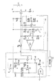
以下、本発明の実施形態を図面に基づいて説明する。まず、車両に搭載されるランプ、モータ等の負荷を駆動させるときに用いる一般的な電力供給回路(オン故障検出装置を備えていない回路)において、スイッチ用のFETにオン故障が発生する過程について説明する。 Hereinafter, embodiments of the present invention will be described with reference to the drawings. First, in a general power supply circuit (a circuit without an on-failure detection device) used when driving a load such as a lamp or a motor mounted on a vehicle, a process in which an on-failure occurs in a switching FET explain.
図1に示すように、負荷RLに駆動用の電力を供給する電力供給回路は、車両に搭載される電源としてのバッテリE(出力電圧VB;例えば直流12ボルト)と、該バッテリEのプラス側出力端子と負荷RLとの間に設けられるN型MOSFET(以下、単に「FET」という)(T1)と、該FET(T1)のゲート(駆動端子)に駆動信号を出力するドライバ回路(駆動回路)1とを備えている。 As shown in FIG. 1, a power supply circuit that supplies driving power to a load RL includes a battery E (output voltage VB; for example, 12 VDC) as a power source mounted on the vehicle, and a positive side of the battery E. An N-type MOSFET (hereinafter simply referred to as “FET”) (T1) provided between the output terminal and the load RL, and a driver circuit (drive circuit) that outputs a drive signal to the gate (drive terminal) of the FET (T1) ) 1.
FET(T1)のドレインは、バッテリEのプラス側端子に接続され、ソースは、負荷RLの一端に接続され、負荷RLの他端はグランドに接地されている。また、バッテリEのプラス側端子はドライバ回路1に接続され、ドライバ回路1に駆動用の電力が供給される。
The drain of the FET (T1) is connected to the positive terminal of the battery E, the source is connected to one end of the load RL, and the other end of the load RL is grounded. The positive terminal of the battery E is connected to the
ドライバ回路1は、チャージポンプ2(出力電圧Vcp;例えば直流10ボルト)と、トランジスタTd1,Td2と、FET(Td3〜Td5)と、抵抗Rd1〜Rd4と、ダイオードDd1と、を備えている。なお、各抵抗Rd1〜Rd4の符号の近傍に記載している数値は、抵抗値の具体例を示す。例えば、抵抗Rd1の抵抗値は、50[KΩ]に設定されていることを示す。
The
ドライバ回路1の具体的な構成について説明すると、バッテリEのプラス側の電源ラインは、ドライバ回路1内で2系統に分岐され、一方の分岐線はチャージポンプ2のマイナス側端子に接続され、他方の分岐線は、ダイオードDd1、抵抗Rd4を介してFET(Td4)(N型)のドレインに接続され、該FET(Td4)のソースはグランドに接地されている。また、FET(Td4)のゲートには、ローアクティブの入力信号電圧Viが供給される。
The specific configuration of the
チャージポンプ2のプラス側端子は、2系統に分岐され、一方の分岐線はトランジスタTd1(NPN型)のコレクタに接続され、そのエミッタはトランジスタTd2(PNP型)のエミッタに接続され、そのコレクタはグランドに接地されている。他方の分岐線は、FET(Td3)(P型)のソースに接続され、そのドレインは抵抗Rd2を介してFET(Td4)のドレインに接続されている。 The positive side terminal of the charge pump 2 is branched into two systems, one branch line is connected to the collector of the transistor Td1 (NPN type), its emitter is connected to the emitter of the transistor Td2 (PNP type), and its collector is Grounded to ground. The other branch line is connected to the source of the FET (Td3) (P-type), and its drain is connected to the drain of the FET (Td4) via the resistor Rd2.
FET(Td3)のゲート・ソース間には抵抗Rd1が設けられ、更に、FET(Td3)のゲートは、抵抗Rd3を介してFET(Td5)(N型)のドレインに接続され、そのソースは、グランドに接地されている。また、FET(Td5)のゲートは、FET(Td4)のドレインに接続されている。 A resistor Rd1 is provided between the gate and source of the FET (Td3), and the gate of the FET (Td3) is connected to the drain of the FET (Td5) (N-type) via the resistor Rd3. Grounded to ground. The gate of the FET (Td5) is connected to the drain of the FET (Td4).
更に、各トランジスタTd1,Td2のベースは、FET(Td4)のドレインに接続されている。また、トランジスタTd1のエミッタとトランジスタTd2のエミッタとの接続点に、駆動信号出力用の配線が接続され、この配線はゲート抵抗Rg(抵抗体)を介してFET(T1)のゲートに接続されている。 Further, the bases of the transistors Td1 and Td2 are connected to the drain of the FET (Td4). Also, a drive signal output wiring is connected to a connection point between the emitter of the transistor Td1 and the emitter of the transistor Td2, and this wiring is connected to the gate of the FET (T1) via a gate resistor Rg (resistor). Yes.
次に、図1に示した電力供給回路の動作について説明する。入力信号電圧Viは、LレベルのときにFET(T1)をオン、HレベルのときにFET(T1)をオフとする、アクティブローで動作する。入力信号電圧ViがLレベルになると、FET(Td4)がオフとなり、トランジスタTd2がオフとなる。更に、FET(Td5),(Td3)、及びトランジスタTd1がオンとなり、バッテリEの電圧VBと約10Vとされているチャージポンプ2の出力電圧Vcpとを加算した電圧(VB+Vcp)が、ドライバ回路1の出力電圧VDとなって、ゲート抵抗Rgを経由してT1のゲートに供給される。これにより、FET(T1)がオンとなり、バッテリEより負荷RLに電力が供給されて該負荷RLが駆動する。
Next, the operation of the power supply circuit shown in FIG. 1 will be described. The input signal voltage Vi operates in an active low state in which the FET (T1) is turned on when it is at L level and the FET (T1) is turned off when it is at H level. When the input signal voltage Vi becomes L level, the FET (Td4) is turned off and the transistor Td2 is turned off. Further, the FETs (Td5), (Td3) and the transistor Td1 are turned on, and the voltage (VB + Vcp) obtained by adding the voltage VB of the battery E and the output voltage Vcp of the charge pump 2 which is about 10 V is added to the
また、入力信号電圧ViがHレベルになると、FET(Td4),トランジスタTd2がオンとなり、FET(Td5),(Td3)、及びトランジスタTd1がオフとなるので、FET(T1)のゲートはゲート抵抗Rg及びトランジスタTd2を経由してグランドに接地される。これにより、FET(T1)はオフとなり、負荷RLへの電力供給が遮断される。 Further, when the input signal voltage Vi becomes H level, the FET (Td4) and the transistor Td2 are turned on, and the FETs (Td5), (Td3) and the transistor Td1 are turned off, so that the gate of the FET (T1) has a gate resistance. It is grounded via Rg and transistor Td2. As a result, the FET (T1) is turned off and the power supply to the load RL is interrupted.
ここで、負荷RLを駆動させるためのFET(T1)が故障する原因の1つとして、ゲートの絶縁層が破壊され、電流のリークが発生することが挙げられる。これはゲートの絶縁層が非常に薄いことがその根源であるので、FET(T1)が故障する原因の中でも大きな割合を占めると考えられている。絶縁層が破壊されるとゲート・ドレイン間、或いはゲート・ソース間に電流のリークが発生する。このうち、ゲート・ソース間での電流のリークでは、ゲート・ソース間が短絡されることになるので、故障が発生したときFET(T1)はオフ状態になり、フェールセーフとなる。従って、安全上の問題は少ない。 Here, one of the causes of failure of the FET (T1) for driving the load RL is that the gate insulating layer is destroyed and current leakage occurs. This is based on the fact that the gate insulating layer is very thin, and is considered to account for a large proportion of the causes of failure of the FET (T1). When the insulating layer is destroyed, current leakage occurs between the gate and the drain or between the gate and the source. Of these, the leakage of current between the gate and the source causes a short circuit between the gate and the source, so that when a failure occurs, the FET (T1) is turned off and becomes fail-safe. Therefore, there are few safety problems.
ところが、ゲート・ドレイン間に生じる電流のリークは、オン故障に繋がるのでフェールセーフとはならず、トラブル発生の原因となってしまう。 However, current leakage between the gate and the drain leads to an on-failure, so that it is not fail-safe and causes trouble.
一般に、電力制御用に用いられるFETは、要素となるFET(以下、「要素FET」という)が複数個並列接続された構成となっており、その要素FETの数は数十万から百万を超えるものになる。従って、絶縁破壊が発生しても、全ての要素FETのゲート・ドレイン間が一度に破壊されるのではなく、一部の要素FETの絶縁破壊から始まり、それが徐々に拡大して行き、最終的にFETのオン故障に至ると考えられる。 In general, FETs used for power control have a structure in which a plurality of FETs as elements (hereinafter referred to as “element FETs”) are connected in parallel, and the number of element FETs ranges from several hundred thousand to one million. It will exceed. Therefore, even if dielectric breakdown occurs, the gate-drain between all the element FETs is not destroyed at once, but it starts with the dielectric breakdown of some element FETs, which gradually expands to the final In particular, it is thought that it leads to an on failure of the FET.
上記の内容を踏まえると、図1に示した回路において、ゲート・ドレイン間の絶縁破壊により、オン故障に至る過程は次の(a)〜(c)に示すようであると推定する。 Based on the above contents, in the circuit shown in FIG. 1, it is presumed that the process leading to the on failure due to the dielectric breakdown between the gate and the drain is as shown in the following (a) to (c).
(a)FET(T1)がオン状態にあるとき、何らかの要因で一部の要素FETがゲート・ドレイン間で絶縁破壊すると、絶縁破壊した要素FETを経由してゲートとドレインが電気的に結合される。ゲート・ドレイン間のリーク抵抗をRa(図1に示す抵抗Raは、このリーク抵抗を等価的に示している)とすると、正常状態では無限大であったRaが絶縁破壊により低下して有限な値となる。但し、リーク抵抗Raは絶縁破壊の程度及びその範囲に依存し、大部分のケースではゲート抵抗Rg(1〜2[KΩ])に比べると初期段階では十分に大きな抵抗値に留まると考えられる。 (A) When the FET (T1) is in an ON state, if some element FET breaks down between the gate and the drain due to some factor, the gate and the drain are electrically coupled via the breakdown element FET. The Assuming that the leakage resistance between the gate and the drain is Ra (the resistance Ra shown in FIG. 1 is equivalent to this leakage resistance), Ra, which is infinite in the normal state, decreases due to dielectric breakdown and becomes finite. Value. However, the leakage resistance Ra depends on the degree and range of dielectric breakdown, and in most cases, it is considered that the leakage resistance Ra remains at a sufficiently large resistance value in the initial stage as compared with the gate resistance Rg (1-2 [KΩ]).
正常状態ではドライバ回路1の出力電圧VDと、FET(T1)のゲート電圧VGが等しくなるが、絶縁破壊が発生してリーク抵抗Raが有限な値になると、該リーク抵抗Raを介してゲートからドレインにリーク電流Igが流れる。そして、リーク電流Igが流れることによりゲート抵抗Rgに電圧降下が発生し、ゲート電圧VGはドライバ回路1の出力電圧VDより低下する。このとき、ゲート電圧VGは、次の(1)式で示される。
In the normal state, the output voltage VD of the
VG=VD−Rg*Ig ・・・(1)
また、絶縁破壊の範囲が広くなるとリーク抵抗Raが小さくなり、リーク電流Igが大きくなって、ゲート電圧VGの低下が大きくなる。従って、リーク電流Igの大きさ、或いはゲート抵抗Rgの電圧降下の大きさを検出することで、FET(T1)に生じる絶縁破壊の程度を把握できることになる。通常、FET(T1)のスレッショルド電圧Vthは4V以下であるので、VG>VB+4V以上であれば、一部の要素FETに絶縁破壊が生じている場合でも、FET(T1)のオン抵抗は正常に近い値に維持され、FET(T1)の発熱量はそれほど増大せず、FET(T1)の熱破壊が急速に進行することはない。
VG = VD-Rg * Ig (1)
Further, when the dielectric breakdown range is widened, the leak resistance Ra is reduced, the leak current Ig is increased, and the gate voltage VG is greatly decreased. Accordingly, by detecting the magnitude of the leakage current Ig or the magnitude of the voltage drop of the gate resistance Rg, the degree of dielectric breakdown occurring in the FET (T1) can be grasped. Normally, the threshold voltage Vth of the FET (T1) is 4 V or less, so if VG> VB + 4 V or more, the on-resistance of the FET (T1) is normal even if some element FETs have dielectric breakdown. It is maintained at a close value, the amount of heat generated by the FET (T1) does not increase so much, and the thermal destruction of the FET (T1) does not proceed rapidly.
(b)FET(T1)をオフとすると、絶縁破壊のない正常な場合はゲート電圧VGがドライバ回路1に設けられたトランジスタTd2を介してグランドに接地され、ゲート電圧VGが約0.6[V]まで低下し、FET(T1)のスレッショルド電圧Vthよりも低くなるので、FET(T1)は遮断される。ところが、FET(T1)が上記(a)の状態、即ち、絶縁破壊されているときは、ドライバ回路1に供給される入力信号電圧ViがHレベルとなり、トランジスタTd2がオンとなっても、FET(T1)のゲート電圧VGは0.6[V]まで低下できず、リーク抵抗Raが小さいときには、ゲート電圧VGが浮き上がってしまい、FET(T1)がオフとならない状態になる。つまり、オン故障となる。
(B) When the FET (T1) is turned off, the gate voltage VG is grounded through the transistor Td2 provided in the
このときのゲート電圧VGは、次の(2)式で示される。 The gate voltage VG at this time is represented by the following equation (2).
VG=VB*Rg/(Ra+Rg) ・・・(2)
なお、(2)式ではトランジスタTd2のエミッタ・ベース間電圧降下を無視している。
VG = VB * Rg / (Ra + Rg) (2)
In the equation (2), the emitter-base voltage drop of the transistor Td2 is ignored.
ゲート電圧VGが、FET(T1)のスレッショルド電圧Vthより大きくなると、ドライバ回路1に供給される入力信号電圧ViがHレベルとなっても、FET(T1)がオフとならないことになる。ここで、ゲート電圧VGがスレッショルド電圧Vthと等しくなるようなリーク抵抗Raを求めると、次の(3)式のようになる。
When the gate voltage VG becomes larger than the threshold voltage Vth of the FET (T1), the FET (T1) is not turned off even if the input signal voltage Vi supplied to the
VG=VB*Rg/(Ra+Rg)=Vth
Ra=Rg(VB−Vth)/Vth ・・・(3)
そして、(3)式より、入力信号電圧ViがHレベルのときに、FET(T1)がオフとならない条件は、次の(3′)式となる。
VG = VB * Rg / (Ra + Rg) = Vth
Ra = Rg (VB−Vth) / Vth (3)
From the equation (3), the condition that the FET (T1) is not turned off when the input signal voltage Vi is at the H level is the following equation (3 ′).
Ra≦Rg(VB−Vth)/Vth ・・・(3′)
通常のN型MOSFETは、スレッショルド電圧Vthは、Vth=2〜4[V]程度である。従って、(3′)式より、ゲート抵抗Rgが大きいほど、バッテリEの電圧VBが大きいほど、及びスレッショルド電圧Vthが小さいほど、リーク抵抗Raが大きくてもFET(T1)はオフとならないことになる。
Ra ≦ Rg (VB−Vth) / Vth (3 ′)
A normal N-type MOSFET has a threshold voltage Vth of about Vth = 2 to 4 [V]. Therefore, from equation (3 ′), the larger the gate resistance Rg, the larger the voltage VB of the battery E, the smaller the threshold voltage Vth, and the larger the leakage resistance Ra, the more the FET (T1) is not turned off. Become.
また、VG>Vthになると、FET(T1)はソースフォロアの動作となり、ドレイン電流をID(負荷RLに流れる電流)とすると、VG−Vth=RL*IDとなるから、ドレイン・ソース間電圧VDSは、次の(4)式で示される。 Further, when VG> Vth, the FET (T1) operates as a source follower, and when the drain current is ID (current flowing through the load RL), VG−Vth = RL * ID, so the drain-source voltage VDS. Is expressed by the following equation (4).
VDS=VB−(VG−Vth)=VB−RL*ID ・・・(4)
このとき、FET(T1)に発生する電力損失をP[W]とすると、電力損失Pは次の(5)式で示される。
VDS = VB- (VG-Vth) = VB-RL * ID (4)
At this time, if the power loss generated in the FET (T1) is P [W], the power loss P is expressed by the following equation (5).
P=VDS*ID
={VB−(VG−Vth)}*ID
={VB−(VG−Vth)}*(VG−Vth)/RL ・・・(5)
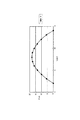
ここで、一例として、VB=12[V]、Vth=2[V]、RL=2[Ω]とし、ゲート電圧VGに対するFET(T1)の電力損失Pをグラフで表すと、図2のようになる。
P = VDS * ID
= {VB- (VG-Vth)} * ID
= {VB- (VG-Vth)} * (VG-Vth) / RL (5)
Here, as an example, when VB = 12 [V], Vth = 2 [V], RL = 2 [Ω], and the power loss P of the FET (T1) with respect to the gate voltage VG is represented by a graph, FIG. become.
図2から理解されるように、ゲート電圧VGがVth=2[V]を超えると電力損失が発生し始め、VG=8[V]で最大となる。具体例としてVG=4[V]を考えると、このとき10[W]の電力損失が発生する。そして、FET(T1)のチャンネルから大気への熱抵抗を20℃/Wとすると200℃の温度上昇となる。ゲート抵抗Rgが1.5[KΩ]の場合は、VG=4Vになるリーク抵抗Raは(2)式より、Ra=3[KΩ]となる。リーク抵抗Raがかなり大きな抵抗値となっている状態から、FET(T1)をオフとした際に、FET(T1)が通電を始める(ドレイン電流が流れる)ことが判る。 As can be understood from FIG. 2, when the gate voltage VG exceeds Vth = 2 [V], power loss starts to occur and becomes maximum at VG = 8 [V]. Considering VG = 4 [V] as a specific example, a power loss of 10 [W] occurs at this time. When the thermal resistance from the FET (T1) channel to the atmosphere is 20 ° C./W, the temperature rises to 200 ° C. When the gate resistance Rg is 1.5 [KΩ], the leakage resistance Ra at which VG = 4 V is Ra = 3 [KΩ] from the equation (2). From the state in which the leak resistance Ra has a considerably large resistance value, it can be seen that when the FET (T1) is turned off, the FET (T1) starts energization (drain current flows).
FET(T1)のオフ時の発熱は、絶縁破壊した要素FETのみならず、正常な要素FETでも同様に発生する。ドレイン電流が流れ始めるとそれがわずかな電流であっても、電圧VDSが大きいので大きな電力損失をもたらし、FET(T1)がオフからオンへ移行する中間領域で大きな電力損失が発生し、VDS=VB/2で最大の電力損失となる。これは絶縁破壊により、ドレイン電流が流れ始めてから、完全にオンとなる、即ち、オン故障状態に至る途中の過程で最大の電力損失となって、大きな発熱を発生させる過程が存在することになり、この過程に滞在する時間が長くなると、FET(T1)がオン故障に至る前にが焼損する可能性があること示す。 The heat generated when the FET (T1) is turned off is generated not only in the element FET that has undergone breakdown but also in a normal element FET. When the drain current starts to flow, even if it is a small current, the voltage VDS is large, resulting in a large power loss, and a large power loss is generated in the intermediate region where the FET (T1) shifts from OFF to ON. VB / 2 is the largest power loss. This is due to dielectric breakdown, and after drain current begins to flow, it is completely turned on, that is, there is a process of generating a large amount of heat due to maximum power loss in the process of reaching the on-failure state. This shows that if the time staying in this process becomes long, the FET (T1) may be burned out before the on failure occurs.
いずれにせよ、オフ状態のFET(T1)にドレイン電流が流れるようになると、電力損失による発熱により、要素FETの絶縁破壊範囲が拡大したり、正常な要素FETが熱破壊したりする可能性が生じる。 In any case, when the drain current flows through the FET (T1) in the off state, there is a possibility that the breakdown range of the element FET is expanded due to heat generation due to power loss, or the normal element FET is thermally destroyed. Arise.
(c)上記(b)の状態でリーク抵抗Raが小さくなったオフ状態のFET(T1)をオンとすると、ゲート抵抗Rgの電圧降下VD−VGが大きくなり、電圧降下VG−VBがVthに近づく。それに連れてFET(T1)のゲート・ソース間電圧が減少するので、FET(T1)のオン時のドレイン・ソース間電圧VDSonが増大し、オン時のFET(T1)の発熱が急速に増大する。正常時のVDSon=50[mV]、Vth=2[V]とすると、VB=VGになるとVDSonは、ほぼVthに等しくなるので、電力損失は正常なときに比べて2[V]/50[mV]=40倍となる。この状態が継続するとFET(T1)は発熱で破壊し、制御不能、即ち、遮断不能となり、オン故障の状態になる。 (C) When the FET (T1) in the off state in which the leakage resistance Ra is reduced in the state of (b) above is turned on, the voltage drop VD-VG of the gate resistance Rg increases and the voltage drop VG-VB becomes Vth. Get closer. Accordingly, since the gate-source voltage of the FET (T1) decreases, the drain-source voltage VDSon when the FET (T1) is on increases, and the heat generation of the FET (T1) when it is on rapidly increases. . When VDSon at normal time is 50 [mV] and Vth = 2 [V], VDSon is almost equal to Vth when VB = VG, so that the power loss is 2 [V] / 50 [50] compared with the normal case. mV] = 40 times. If this state continues, the FET (T1) breaks down due to heat generation, becomes uncontrollable, that is, cannot be shut off, and enters an on-failure state.
上記の内容をまとめると、要素FETの一部がゲート・ドレイン間の絶縁破壊を起こすと、FET(T1)のオフ時にリーク電流を発生させ、発熱を生じる。オフ時の熱破壊が進行すると、FET(T1)のオン時のゲート・ソース間電圧が低下し、オン時の発熱が増大する。オフ時の発熱とオン時の発熱のメカニズムは異なり、オフ時の発熱は絶縁破壊の前半で大きくなり、オン時の発熱は絶縁破壊が進行した後半で大きくなる。この2つの発熱メカニズムが重なり合って作用し、ついには熱破壊により、オン故障状態に至ると考えられる。 In summary, when a part of the element FET causes breakdown between the gate and the drain, a leak current is generated when the FET (T1) is turned off, and heat is generated. When the thermal breakdown at the OFF time proceeds, the gate-source voltage when the FET (T1) is turned on decreases, and the heat generation at the ON time increases. The heat generation mechanism at the time of off is different from the mechanism of heat generation at the time of on. The heat generation at the time of off is large in the first half of the dielectric breakdown, and the heat generation in the on is large in the latter half of the breakdown. It is thought that these two heat generation mechanisms act in an overlapping manner, and eventually an on-failure state is reached due to thermal destruction.
従って、上記(a)〜(c)に示した内容を踏まえ、本発明では、以下に示す(イ)、(ロ)の考え方を採用する。 Therefore, based on the contents shown in the above (a) to (c), the present invention adopts the following concepts (a) and (b).
(イ)一部の要素FETのゲート・ドレイン間に絶縁破壊が発生し、それがトリガーとなって、その後のFET(T1)の熱破壊を引き起こす過程では、それが進行するに連れてリーク抵抗Raが減少し、Raの減少はゲート抵抗Rgに流れるリーク電流Igの増大となり、ゲート抵抗Rgの電圧降下の増大となる。従って、FET(T1)がオンしているときのゲート抵抗Rgの電圧降下を測定すれば、絶縁破壊に起因したオン故障を事前に察知できる。即ち、完全にオン故障に至る前の段階で、オン故障の兆候を察知できる。そのときの検出感度は、ゲート抵抗Rgが大きいほど良くなる。 (A) In the process where dielectric breakdown occurs between the gate and drain of some element FETs, which triggers the subsequent thermal breakdown of the FET (T1), leakage resistance as it progresses Ra decreases, and the decrease of Ra increases the leakage current Ig flowing through the gate resistance Rg, and increases the voltage drop of the gate resistance Rg. Therefore, by measuring the voltage drop of the gate resistance Rg when the FET (T1) is on, it is possible to detect in advance an on failure due to dielectric breakdown. That is, a sign of an on-failure can be detected at a stage prior to a complete on-failure. The detection sensitivity at that time increases as the gate resistance Rg increases.
(ロ)オン故障に至る現象を上記(イ)に記載した手順で察知したら、FET(T1)を遮断する。遮断するためには、ドライバ回路1の出力信号をグランドに接地したときに、VG<Vthとなるようにしなければならない。これは、FET(T1)のゲートとグランドとの間の抵抗が小さいほど実現し易い。即ち、オフ時のゲート・グランド間の抵抗が、ゲート抵抗Rgよりも小さくなるような回路構成にする。
(B) When a phenomenon leading to an on failure is detected by the procedure described in (a) above, the FET (T1) is shut off. In order to cut off, it is necessary to satisfy VG <Vth when the output signal of the
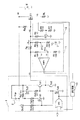
以下、上記の考え方を採用して構成した本発明の実施形態について説明する。図3は、本発明の第1の実施形態に係る電力供給回路のオン故障検出装置の構成を示す回路図である。なお、図3において、図1に示した電力供給回路と同一の構成要素については、同一の符号を付して、その構成説明を省略する。 Hereinafter, an embodiment of the present invention configured by adopting the above concept will be described. FIG. 3 is a circuit diagram showing the configuration of the on-failure detection device for the power supply circuit according to the first embodiment of the present invention. In FIG. 3, the same components as those of the power supply circuit shown in FIG.
図3に示す電力供給回路は、図1に示した回路に対して、オン故障判定回路(オン故障判定手段)11、ゲート接地回路(接地手段)12、及び遅延回路13を備え、且つ、ドライバ回路1がオア回路OR1を備えている点で相違している。
The power supply circuit shown in FIG. 3 includes an on-failure determination circuit (on-failure determination means) 11, a gate grounding circuit (grounding means) 12, and a
オン故障判定回路11は、FET(T1)のゲートとグランドとの間に設けられる抵抗R1とR2との直列接続回路と、バッテリEのプラス側端子(電圧VB)とグランドとの間に設けられる抵抗R3,R4及び直流電源3(出力電圧VA)の直列接続回路を備えている。更に、比較器CMP1(比較手段)を備えており、抵抗R1とR2との接続点P1が比較器CMP1の反転入力端子に接続され、抵抗R3とR4との接続点P2が比較器CMP1の正転入力端子に接続されている。
The on-
また、比較器CMP1の出力端子は、遅延回路13に接続されている。遅延回路13の出力端子は、ドライバ回路1に設けられたオア回路OR1の一方の入力端子に接続され、他方の入力端子には、入力信号電圧Viが供給されるようになっている。遅延回路13は、スタート時、リセットにより出力がLレベルになるように設定されている。なお、図3の各抵抗R1〜R7の近傍に示す値は、各抵抗R1〜R7の抵抗値の具体例を示している。例えば、抵抗R1の抵抗値は100[KΩ]とされている。
The output terminal of the comparator CMP1 is connected to the
ゲート接地回路12は、FET(T1)のゲートをグランドに接地するためのトランジスタT2(NPN型)と、該トランジスタT2のコレクタとFET(T1)のゲートとの間に設けられる抵抗R5と、オア回路OR1の出力端子とグランドとの間に設けられる抵抗R6とR7との直列接続回路とを備えており、抵抗R6とR7の接続点P3は、トランジスタT2のベースに接続されている。なお、抵抗R5の抵抗値は、例えば100[Ω]であり、例えば、1.5[KΩ]の抵抗値を有するゲート抵抗Rgよりも小さい値に設定されている。
The
次に、上記のように構成された本実施形態に係るオン故障検出装置の作用について説明する。ここで、各抵抗R1〜R4を、R1=R2、R3=R4となるように抵抗値を選定する。また、比較器CMP1の反転入力端子(点P1)及び正転入力端子(点P2)の電圧をそれぞれV1、V2とし、直流電源3の出力電圧(これを「基準電圧」という)をVAとする。 Next, the operation of the on-failure detection apparatus according to the present embodiment configured as described above will be described. Here, the resistance values of the resistors R1 to R4 are selected so that R1 = R2 and R3 = R4. Further, the voltages of the inverting input terminal (point P1) and the normal rotation input terminal (point P2) of the comparator CMP1 are V1 and V2, respectively, and the output voltage of the DC power supply 3 (this is referred to as “reference voltage”) is VA. .
いま、R2/(R1+R2)=R4/(R3+R4)=a(aは分圧比)、VG−VB=δとおくと、以下の(6)式が得られる。 Now, assuming that R2 / (R1 + R2) = R4 / (R3 + R4) = a (a is a voltage division ratio) and VG−VB = δ, the following expression (6) is obtained.
V1=VG*a=(VB+δ)a
V2=(VB−VA)a+VA ・・・(6)
上記(6)式から、V1=V2となるときのδを求めると、次の(7)式となる。
V1 = VG * a = (VB + δ) a
V2 = (VB−VA) a + VA (6)
From the above equation (6), when δ when V1 = V2 is obtained, the following equation (7) is obtained.
(VB+δ)a=(VB−VA)a+VA
δ=VA*(1−a)/a ・・・(7)
上記(7)式より、V1=V2となるときのδ、即ち比較器CMP1出力が反転するときのδは、基準電圧VAと分圧比aにより、任意の値に設定できる。例えば、VA=4[V]、a=0.5とすると、δ=4[V]となる。即ち、VG>(VB+4[V])であれば、比較器CMP1の出力はLレベルとなり、VG<(VB+4[V])であれば比較器CMP1の出力はHレベルになる。
(VB + δ) a = (VB−VA) a + VA
δ = VA * (1-a) / a (7)
From the above equation (7), δ when V1 = V2, that is, δ when the output of the comparator CMP1 is inverted can be set to an arbitrary value by the reference voltage VA and the voltage dividing ratio a. For example, if VA = 4 [V] and a = 0.5, then δ = 4 [V]. That is, if VG> (VB + 4 [V]), the output of the comparator CMP1 is L level, and if VG <(VB + 4 [V]), the output of the comparator CMP1 is H level.
一方、FET(T1)がオンとなっているときには、ドライバ回路1の出力電圧VDはVB+Vcpであるから、ゲート抵抗Rgの電圧降下となるRg*Igは、次の(8)式で示される。
On the other hand, since the output voltage VD of the
Rg*Ig=VD−VG=(VB+Vcp)−(VB+δ)=Vcp−δ・・・(8)
よって、Vcp=10[V]、δ=4[V]のときは、6[V]以上の電圧降下がゲート抵抗Rgに発生しているとき、比較器CMP1出力はHレベルになる。比較器CMP1の出力がHレベルになり、それが所定の時間継続するとゲート・ドレイン間に絶縁破壊が発生したと判断して、オア回路OR1出力をHレベルにする。即ち、比較器CMP1の出力信号がHレベルとなると、遅延回路13にて所定時間経過した後に、ドライバ回路1のオア回路OR1の一方の入力端子にHレベルの信号が入力されるので、該オア回路ORの出力信号がHレベルとなる。これにより、ドライバ回路1の出力がトランジスタTd2を介して接地され、同時にトランジスタT2のベースとなる点P3の電圧が一定のレベルに上昇するので、該トランジスタT2がオンとなり、FET(T1)のゲートはゲート抵抗Rgと抵抗R5の並列合成抵抗(「Rg‖R5」と表記する)により接地される。
Rg * Ig = VD−VG = (VB + Vcp) − (VB + δ) = Vcp−δ (8)
Therefore, when Vcp = 10 [V] and δ = 4 [V], when a voltage drop of 6 [V] or more occurs in the gate resistance Rg, the output of the comparator CMP1 becomes H level. When the output of the comparator CMP1 becomes H level and continues for a predetermined time, it is determined that dielectric breakdown has occurred between the gate and the drain, and the OR circuit OR1 output is set to H level. That is, when the output signal of the comparator CMP1 becomes H level, after a predetermined time elapses in the
このときのゲート電圧VGは、次の(9)式で示される。 The gate voltage VG at this time is expressed by the following equation (9).
VG=VB*(Rg‖R5)/{(Rg‖R5)+Ra} ・・・(9)
ここで、抵抗R5を設けないときと比較し、同一のリーク抵抗Raに対してゲート電圧VGが小さくなり、VG<Vthを満足し易くなる。
VG = VB * (Rg‖R5) / {(Rg‖R5) + Ra} (9)
Here, as compared with the case where the resistor R5 is not provided, the gate voltage VG is reduced with respect to the same leakage resistance Ra, and VG <Vth is easily satisfied.
ゲート抵抗Rgを大きくするとゲートからドレインへのリーク電流Igの検出が敏感になり、抵抗R5を小さくするとリーク抵抗Raが小さなところまで、FET(T1)を遮断できるようになる。このように、ゲート抵抗Rg及び抵抗R5の抵抗値を適宜選定することにより、ゲート・ドレイン間の絶縁破壊(要素FETによる部分的な絶縁破壊)を検出し、FET(T1)が未だ遮断能力を有している時点でFET(T1)を遮断して、該FET(T1)がオン故障に至ることを防止することが可能となる。 Increasing the gate resistance Rg makes the detection of the leak current Ig from the gate to the drain sensitive, and decreasing the resistance R5 makes it possible to cut off the FET (T1) up to a point where the leakage resistance Ra is small. Thus, by appropriately selecting the resistance values of the gate resistance Rg and the resistance R5, the dielectric breakdown between the gate and the drain (partial dielectric breakdown due to the element FET) is detected, and the FET (T1) still has the blocking capability. It is possible to prevent the FET (T1) from being turned on by blocking the FET (T1) at the time of holding.
このようにして、第1の実施形態に係るオン故障検出装置では、FET(T1)に絶縁破壊が発生し、リーク電流が増大して点P1の電圧V1が低下し、点P2の電圧V2を下回った場合に、ドライバ回路1の出力をグランドに接地してFET(T1)に供給する駆動信号を停止させるので、FET(T1)がオン故障となる前の時点で該FET(T1)をオフとして、FET(T1)及び負荷、電気配線などの回路構成部品を保護することができる。
In this manner, in the on-failure detection apparatus according to the first embodiment, the breakdown occurs in the FET (T1), the leakage current increases, the voltage V1 at the point P1 decreases, and the voltage V2 at the point P2 is reduced. If the output is lower, the drive signal supplied to the FET (T1) is stopped by grounding the output of the
また、ドライバ回路1の出力をグランドに接地すると同時に、ゲート接地回路12のトランジスタT2をオンとして、FET(T1)のゲートを抵抗R5(R5<Rg)を介してグランドに接地するので、確実にゲート電圧VGをスレッショルド電圧Vthよりも小さくすることができ、確実にFET(T1)をオフとすることができる。
Also, since the output of the
更に、第1の実施形態では、FET(T1)のゲート電圧が低下する、リーク抵抗Raの低下以外の要因として、ドライバ回路1に設けられたチャージポンプ2の電圧降下が挙げられる。つまり、リーク抵抗Raが無限大に大きい状態(絶縁破壊が発生していない状態)でも、チャージポンプ2の出力電圧が低下した場合には、点P1の電圧V1が点P2の電圧V2を下回ってしまい、FET(T1)をオフとする。従って、チャージポンプ2の出力電圧が低下したことも併せて検出することができる。
Furthermore, in the first embodiment, the voltage drop of the charge pump 2 provided in the
次に、本実施形態の第2の実施形態について説明する。図4は、第2の実施形態に係る電力供給回路のオン故障検出装置の構成を示す回路図である。第2の実施形態では、図3に示した第1の実施形態と比較して、オン故障判定回路(オン故障判定手段)11の構成のみが相違しているので、構成については相違点のみ説明する。 Next, a second embodiment of the present embodiment will be described. FIG. 4 is a circuit diagram showing a configuration of the on-failure detection device for the power supply circuit according to the second embodiment. In the second embodiment, only the configuration of the on-failure determination circuit (on-failure determination means) 11 is different from the first embodiment shown in FIG. To do.
図4に示すオン故障判定回路11は、FET(T1)のゲート抵抗Rgのドライバ回路1側となる端子とグランドとの間に、抵抗R1とR2の直列接続回路を備え、且つ、ゲート抵抗RgのFET(T1)側となる端子とグランドとの間に、抵抗R3、R4、及び直流電源3の直列接続回路を備えている。そして、抵抗R1とR2の接続点P11(電圧V1;第1の電圧)が比較器CMP1の正転入力端子に接続され、抵抗R3とR4の接続点P12(電圧V2;第2の電圧)が比較器CMP1の反転入力端子に接続されている。
The on-
そして、直流電源3より出力される基準電圧VAを6[V]に設定すると、この回路ではゲート抵抗Rgの電圧降下が6V以上になると、比較器CMP1の出力信号がLレベルからHレベルに反転し、ドライバ回路1に設けられたトランジスタTd2、及びゲート接地回路12のトランジスタT2をオンとして、FET(T1)のゲートを、ゲート抵抗Rgと抵抗R5の並列経路を介してグランドに接地する。即ち、図4に示す第2の実施形態では、ゲート抵抗Rgの電圧降下を直接測定し、測定された電圧が所定のレベルに達して、所定の時間継続した場合に、FET(T1)のゲート・ドレイン間に絶縁破壊が生じているものと判定し、ゲートを接地してFET(T1)を遮断するようにしている。
When the reference voltage VA output from the DC power supply 3 is set to 6 [V], the output signal of the comparator CMP1 is inverted from the L level to the H level when the voltage drop of the gate resistance Rg becomes 6 V or more in this circuit. Then, the transistor Td2 provided in the
このようにして、第2の実施形態に係る電力供給回路のオン故障検出装置では、ゲート抵抗Rgにおける電圧降下に基づいて、FET(T1)のゲート・ドレイン間に絶縁破壊が生じているか否かを判定し、絶縁破壊が発生している場合には、FET(T1)をオフとするので、絶縁破壊によるオン故障の発生を防止できる。 In this way, in the on-failure detection apparatus for the power supply circuit according to the second embodiment, whether or not dielectric breakdown occurs between the gate and the drain of the FET (T1) based on the voltage drop in the gate resistance Rg. If the dielectric breakdown has occurred, the FET (T1) is turned off, so that an on failure due to the dielectric breakdown can be prevented.
また、ゲート抵抗Rgの両端電圧に基づいて、リーク電流の発生を検出する構成であるので、前述した第1の実施形態と比較して、チャージポンプ2の出力電圧の低下に関係なく、FET(T1)の絶縁破壊のみを検出することができる。 Further, since the generation of the leakage current is detected based on the voltage across the gate resistance Rg, the FET ((2) is not related to the decrease in the output voltage of the charge pump 2 as compared with the first embodiment described above. Only the dielectric breakdown of T1) can be detected.
次に、本発明の第3の実施形態について説明する。図5は、第3の実施形態に係る電力供給回路のオン故障検出装置の構成を示す回路図である。 Next, a third embodiment of the present invention will be described. FIG. 5 is a circuit diagram showing a configuration of an on-fault detection device for a power supply circuit according to the third embodiment.
上述した第1,第2の実施形態では、負荷RLの駆動、停止を切り替えるための半導体素子として、N型MOSFET(T1)を用いる場合を例に挙げて説明したが、第3の実施形態では、P型MOSFET(T11)を用いている点、及びこれに伴う各回路構成が上記第1,第2の実施形態と相違する。 In the first and second embodiments described above, the case where the N-type MOSFET (T1) is used as the semiconductor element for switching between driving and stopping of the load RL has been described as an example, but in the third embodiment, The P-type MOSFET (T11) is used, and each circuit configuration associated therewith is different from the first and second embodiments.
以下、具体的な回路構成について説明する。バッテリEと負荷RLとの間に設けられる半導体素子としてのP型MOSFET(以下、単に「FET」という)(T11)は、ソースがバッテリEのプラス側端子に接続され、ドレインが負荷RLの一端に接続されている。 A specific circuit configuration will be described below. A P-type MOSFET (hereinafter simply referred to as “FET”) (T11) as a semiconductor element provided between the battery E and the load RL has a source connected to the positive terminal of the battery E and a drain connected to one end of the load RL. It is connected to the.
また、FET(T11)のゲートに駆動信号を出力するドライバ回路31と、オン故障判定回路21と、ゲート・電源接続回路(電源接続手段)22と、遅延回路13と、を備えている。
In addition, a
ドライバ回路31は、抵抗Rd1,Rd2と、FET(Td3),(Td4)(N型)と、トランジスタTd1(NPN型),Td2(PNP型)とオア回路OR11と、を備えている。具体的な構成として、ドライバ回路31に接続されるバッテリEの電源線は3系統に分岐され、1つ目は、抵抗Rd2とFET(Td4)を介してグランドに接続され、2つ目は、抵抗Rd1とFET(Td3)を介してグランドに接続され、3つ目は、トランジスタTd1,Td2を介してグランドに接続されている。
The
2つのトランジスタTd1,Td2の各ベースは、FET(Td3)のドレインに接続され、該FET(Td3)のゲートは、FET(Td4)のドレインに接続されている。そして、トランジスタTd1のエミッタと、トランジスタTd2のエミッタとの接続点が、ドライバ回路31の出力電圧VDを出力するための配線に接続されている。
The bases of the two transistors Td1 and Td2 are connected to the drain of the FET (Td3), and the gate of the FET (Td3) is connected to the drain of the FET (Td4). A connection point between the emitter of the transistor Td1 and the emitter of the transistor Td2 is connected to a wiring for outputting the output voltage VD of the
FET(Td4)のゲートは、オア回路OR11の出力端子に接続され、該オア回路OR11の一方の入力端子には、遅延回路13の出力端子が接続され、他方の入力端子には、入力信号電圧Viが供給される。
The gate of the FET (Td4) is connected to the output terminal of the OR circuit OR11, one output terminal of the OR circuit OR11 is connected to the output terminal of the
オン故障判定回路21は、FET(T11)のゲートとグランドとの間に設けられる抵抗R1とR2の直列接続回路と、比較器CMP11(比較手段)と、直流電源23(出力電圧VA)とを備えている。そして、比較器CMP11の正転入力端子には、抵抗R1とR2の接続点P21(電圧V11)が接続され、反転入力端子には、直流電源23のプラス側出力端子が接続されている。また、比較器CMP11の出力端子は、遅延回路13に接続されている。
The on-
ゲート・電源接続回路22は、P型MOSFET(T12)と、抵抗R5の直列接続回路を備えており、FET(T12)のソースはバッテリEのプラス側出力端子に接続され、ドレインは抵抗R5の一端に接続され、該抵抗R5の他端はFET(T11)のゲートに接続されている。また、FET(T12)のゲートは、FET(Td4)のドレインに接続されている。
The gate / power
次に、上記のように構成された第3の実施形態の動作について説明する。入力信号電圧ViがHレベルからLレベルになると、遅延回路13は初期的にLレベルにリセットされるように構成されているので、オア回路OR11の出力信号がLレベルになり、FET(Td4)がオフとなり、これにより、FET(Td3)、及びトランジスタTd2がオンとなって、FET(T11)のゲートがゲート抵抗Rgを経由してグランドに接地される。その結果、FET(T11)がオンとなる。
Next, the operation of the third embodiment configured as described above will be described. When the input signal voltage Vi is changed from the H level to the L level, the
FET(T11)のゲート・ドレイン間の抵抗をリーク抵抗Raとすると、正常状態ではリーク抵抗Raは無限大であるが、FET(T11)のゲート・ドレイン間に絶縁破壊が発生するとリーク抵抗Raが有限の値になり、FET(T11)のドレイン→ゲート→ゲート抵抗Rg→トランジスタTd2→グランドの経路でリーク電流Igが流れ、ゲート抵抗Rgに電圧降下が発生する。 Assuming that the resistance between the gate and drain of the FET (T11) is the leakage resistance Ra, the leakage resistance Ra is infinite in the normal state, but when the dielectric breakdown occurs between the gate and drain of the FET (T11), the leakage resistance Ra is reduced. It becomes a finite value, and a leak current Ig flows through the drain of the FET (T11) → gate → gate resistance Rg → transistor Td2 → ground, and a voltage drop occurs in the gate resistance Rg.
ここで、オン故障判定回路21の抵抗をR1=R2、及び基準電圧VA=3Vに設定しておくと、リーク電流Igが増加してRg*Igが6Vを超えると、比較器CMP11の出力がHレベルになり、その状態が所定の時間継続するとオア回路OR11の出力がHレベルになる。これによりFET(Td4)がオンとなり、FET(Td3)、及びトランジスタTd2が共にオフとなり、トランジスタ(Td1)がオンとなって、FET(T11)のゲートがゲート抵抗Rgを経由してバッテリEの電圧VBに引き上げられる。更に、FET(T2)のゲートがFET(Td4)がオンとなることによりグランドに接地されるので、FET(T2)がオンとなり、FET(T11)のゲートは低抵抗R5を介して電源VBに接続される。これによりRg*Ig>6Vであっても、FET(T11)を確実に遮断することができる。
Here, if the resistance of the on-
このようにして、第3の実施形態に係る電力供給回路のオン故障検出装置では、負荷の駆動、停止を切り替える半導体素子として、P型MOSFET(T11)を用いた場合であっても、前述した第2の実施形態の場合と同様に、FET(T11)のゲート・ドレイン間に絶縁破壊が発生し、リーク電流が流れるようになった場合には、ゲート抵抗Rgに生じる電圧降下を検出して、絶縁破壊の発生をいち早く検出することができ、確実にFET(T11)を遮断させることができる。 As described above, in the on-failure detection device for the power supply circuit according to the third embodiment, even when the P-type MOSFET (T11) is used as the semiconductor element for switching between driving and stopping of the load, the above-described case is described. As in the case of the second embodiment, when a dielectric breakdown occurs between the gate and drain of the FET (T11) and a leak current starts to flow, the voltage drop generated in the gate resistance Rg is detected. Thus, the occurrence of dielectric breakdown can be detected promptly, and the FET (T11) can be reliably cut off.
以上、本発明の電力供給回路のオン故障検出装置を図示の実施形態に基づいて説明したが、本発明はこれに限定されるものではなく、各部の構成は、同様の機能を有する任意の構成のものに置き換えることができる。 As mentioned above, although the on-failure detection device for the power supply circuit of the present invention has been described based on the illustrated embodiment, the present invention is not limited to this, and the configuration of each part is an arbitrary configuration having the same function Can be replaced.
例えば、上述した各実施形態では、電源として車両に搭載されるバッテリ、負荷として車両に搭載されるランプ、モータ等を用いた場合の例について説明したが、本発明はこれに限定されるものではなく、その他の電力供給回路についても適用することができる。 For example, in each of the above-described embodiments, an example in which a battery mounted on a vehicle as a power source, a lamp mounted on the vehicle as a load, a motor, or the like has been described, but the present invention is not limited to this. However, the present invention can be applied to other power supply circuits.
また、上述した実施形態では、スイッチ用の半導体素子としてN型、またはP型のMOSFETを用いる例について説明したが、本発明はこれに限定されるものではなく、IGBT(絶縁ゲートバイポーラトランジスタ)等についても適用が可能である。 In the above-described embodiment, an example in which an N-type or P-type MOSFET is used as a semiconductor element for switching has been described. However, the present invention is not limited to this, and an IGBT (insulated gate bipolar transistor) or the like is used. Is also applicable.
スイッチング用の半導体素子にオン故障が発生する兆候を検出し、遮断機能が損なわれないうちに半導体素子を遮断して、回路を保護する上で極めて有用である。 It is extremely useful for detecting a sign that an on-failure occurs in a semiconductor element for switching and protecting the circuit by shutting off the semiconductor element before the shut-off function is impaired.
1,31 ドライバ回路(駆動回路)
2 チャージポンプ
3,23 直流電源
11,21 オン故障判定回路(オン故障判定手段)
12 ゲート接地回路(接地手段)
22 ゲート・電源接続回路(電源接続手段)
E バッテリ(電源)
T1,T11 MOSFET(半導体素子)
CMP1 比較器(比較手段)
1,31 Driver circuit (Drive circuit)
2
12 Gate grounding circuit (grounding means)
22 Gate / power supply connection circuit (power supply connection means)
E Battery (Power)
T1, T11 MOSFET (semiconductor element)
CMP1 comparator (comparison means)
Claims (3)
前記N型MOSFETのゲート端子に、該N型MOSFETのオン、オフを切り換えるための、前記電源電圧に基づく駆動信号を供給する駆動回路と、
前記駆動回路と前記ゲート端子との間に設けられる抵抗体と、
前記ゲート端子に駆動信号を供給し始めてから一定時間経過後の、前記ゲート端子に生じる電圧に基づいて生成される第1電圧、及び前記電源電圧に基づいて生成される第2電圧との差分電圧を検出し、この差分電圧が所定値を超えている場合に、前記N型MOSFETにオン故障が生じているものと判定するオン故障判定手段と、
を備えることを特徴とする電力供給回路のオン故障検出装置。 An N-type MOSFET is disposed between a power source and a load, the drain of the N-type MOSFET is connected to the power source side, the source is connected to the load side, and the N-type MOSFET is switched on and off. In the on-failure detection device for detecting the on-failure of the N-type MOSFET of the power supply circuit that controls driving and stopping of the load,
A drive circuit for supplying a drive signal based on the power supply voltage for switching on and off the N-type MOSFET to the gate terminal of the N-type MOSFET ;
A resistor provided between the drive circuit and the gate terminal;
Wherein after a predetermined time has elapsed from the start of supplying the driving signal to the gate terminal, a first voltage is generated based on the voltage generated at the gate terminal, and a difference voltage between the second voltage is generated based on the power supply voltage And when the differential voltage exceeds a predetermined value, an on-failure determining means for determining that an on-failure has occurred in the N-type MOSFET ,
An on-failure detection device for a power supply circuit comprising:
Priority Applications (5)
| Application Number | Priority Date | Filing Date | Title |
|---|---|---|---|
| JP2005366416A JP4776368B2 (en) | 2005-12-20 | 2005-12-20 | On-fault detection device for power supply circuit |
| EP06024144A EP1801974B1 (en) | 2005-12-20 | 2006-11-21 | Power supply circuit having on-failure detecting apparatus |
| KR1020060116165A KR101076764B1 (en) | 2005-12-20 | 2006-11-23 | On failure detection apparatus of power supply circuit |
| US11/640,216 US7504849B2 (en) | 2005-12-20 | 2006-12-18 | On failure detecting apparatus of power supply circuit |
| CN2006101690546A CN1988385B (en) | 2005-12-20 | 2006-12-20 | On failure detection apparatus of power supply circuit |
Applications Claiming Priority (1)
| Application Number | Priority Date | Filing Date | Title |
|---|---|---|---|
| JP2005366416A JP4776368B2 (en) | 2005-12-20 | 2005-12-20 | On-fault detection device for power supply circuit |
Publications (2)
| Publication Number | Publication Date |
|---|---|
| JP2007174756A JP2007174756A (en) | 2007-07-05 |
| JP4776368B2 true JP4776368B2 (en) | 2011-09-21 |
Family
ID=37912432
Family Applications (1)
| Application Number | Title | Priority Date | Filing Date |
|---|---|---|---|
| JP2005366416A Expired - Fee Related JP4776368B2 (en) | 2005-12-20 | 2005-12-20 | On-fault detection device for power supply circuit |
Country Status (5)
| Country | Link |
|---|---|
| US (1) | US7504849B2 (en) |
| EP (1) | EP1801974B1 (en) |
| JP (1) | JP4776368B2 (en) |
| KR (1) | KR101076764B1 (en) |
| CN (1) | CN1988385B (en) |
Families Citing this family (23)
| Publication number | Priority date | Publication date | Assignee | Title |
|---|---|---|---|---|
| US8593773B2 (en) | 2008-11-05 | 2013-11-26 | Osram Gesellschaft Mit Berschraenkter Haftung | Half-bridge circuit protected against short circuits and having semiconductor switches |
| JP4973703B2 (en) * | 2009-07-30 | 2012-07-11 | 富士通株式会社 | Failure detection method and monitoring device |
| JP2011071174A (en) | 2009-09-24 | 2011-04-07 | Renesas Electronics Corp | Semiconductor device and method of detecting characteristic degradation of semiconductor device |
| JP5484094B2 (en) * | 2010-01-25 | 2014-05-07 | リンナイ株式会社 | Combustion device |
| KR102005450B1 (en) * | 2012-03-14 | 2019-07-30 | 삼성전자주식회사 | Power module comprising leakage current protecting circuit |
| JP6164429B2 (en) | 2012-05-01 | 2017-07-19 | 大島俊蔵 | Overcurrent protection power supply |
| JP6187904B2 (en) * | 2013-06-11 | 2017-08-30 | ローム株式会社 | Electronic circuit |
| CN104237761B (en) * | 2013-06-13 | 2018-05-04 | 通用电气公司 | The system and method for the failure mode detection and protection of insulated gate bipolar transistor |
| CN104422806B (en) * | 2013-08-21 | 2018-08-07 | 鸿富锦精密工业(深圳)有限公司 | Power sensor detecting circuit |
| JP6396041B2 (en) | 2014-03-11 | 2018-09-26 | 三菱重工サーマルシステムズ株式会社 | Vehicle and failure detection method |
| FR3021823B1 (en) * | 2014-05-27 | 2017-10-20 | Renault Sas | FIELD EFFECT TRANSISTOR AND ASSOCIATED FAILURE DETECTION DEVICE |
| US10371752B2 (en) * | 2015-04-23 | 2019-08-06 | Infineon Technologies Austria Ag | Switch device |
| US10312804B2 (en) | 2016-02-05 | 2019-06-04 | Shunzou Ohshima | Power supply apparatus with power factor correction using fixed on and off periods |
| JPWO2018168328A1 (en) | 2017-03-14 | 2020-01-16 | 日本電産株式会社 | Power semiconductor switching device damage prediction device and damage prediction method, AC-DC converter, DC-DC converter |
| DE112018005588T5 (en) * | 2017-10-17 | 2020-07-16 | Fuji Electric Co., Ltd. | OVERCURRENT DETECTING DEVICE, CONTROL DEVICE AND OVERCURRENT DETECTING METHOD |
| US10432175B2 (en) * | 2018-01-10 | 2019-10-01 | Texas Instruments Incorporated | Low quiescent current load switch |
| JP6770986B2 (en) * | 2018-03-06 | 2020-10-21 | 日本電産モビリティ株式会社 | Inductive load controller |
| KR102382253B1 (en) * | 2018-10-30 | 2022-04-01 | 주식회사 엘지에너지솔루션 | Driver circuit for main transistor and control device including the same |
| CN112054564B (en) * | 2019-06-05 | 2022-07-19 | Oppo广东移动通信有限公司 | Circuit detection method and device, equipment and storage medium |
| DE102020103874B3 (en) | 2020-02-14 | 2021-06-10 | Infineon Technologies Ag | PROCEDURE AND CIRCUIT FOR CHECKING THE FUNCTIONALITY OF A TRANSISTOR COMPONENT |
| WO2021199682A1 (en) * | 2020-03-30 | 2021-10-07 | ローム株式会社 | Mirror clamp circuit |
| CN111474460B (en) * | 2020-05-29 | 2022-03-22 | 中煤科工集团重庆研究院有限公司 | IGBT grid resistance fault detection system |
| JP7414700B2 (en) | 2020-12-01 | 2024-01-16 | 株式会社東芝 | semiconductor equipment |
Family Cites Families (19)
| Publication number | Priority date | Publication date | Assignee | Title |
|---|---|---|---|---|
| JP2914841B2 (en) | 1992-04-14 | 1999-07-05 | リンナイ株式会社 | Electromagnetic safety valve maintenance system |
| US5486772A (en) * | 1994-06-30 | 1996-01-23 | Siliconix Incorporation | Reliability test method for semiconductor trench devices |
| JP3608835B2 (en) | 1995-03-30 | 2005-01-12 | リンナイ株式会社 | Safety monitoring device for electromagnetic safety valve |
| JP3336488B2 (en) * | 1995-04-25 | 2002-10-21 | 株式会社日立製作所 | Gate drive device for voltage driven devices |
| JPH09331625A (en) * | 1996-06-11 | 1997-12-22 | Yazaki Corp | Intelligent power switch and switching device |
| JP3911049B2 (en) * | 1996-07-16 | 2007-05-09 | ソニー株式会社 | Charger |
| US6011416A (en) * | 1997-02-19 | 2000-01-04 | Harness System Technologies Research Ltd. | Switch circuit having excess-current detection function |
| JP4116693B2 (en) | 1998-05-20 | 2008-07-09 | 松下電器産業株式会社 | Low power semiconductor integrated circuit for leak current and leak inspection method |
| US5984394A (en) * | 1998-06-26 | 1999-11-16 | Bergeron; Raymond E. | Power bucket |
| JP3034508B1 (en) * | 1998-11-12 | 2000-04-17 | 本田技研工業株式会社 | Motor drive |
| JP2001211059A (en) | 2000-01-26 | 2001-08-03 | Toshiba Corp | Overcurrent protection circuit for semiconductor switch device |
| JP4434510B2 (en) * | 2001-03-16 | 2010-03-17 | 株式会社東芝 | Fault detection method and fault detection apparatus for insulated gate semiconductor device |
| JP3780898B2 (en) * | 2001-10-16 | 2006-05-31 | 富士電機デバイステクノロジー株式会社 | Power device drive circuit |
| JP3931627B2 (en) * | 2001-11-01 | 2007-06-20 | 株式会社日立製作所 | Gate driving device for semiconductor switching element |
| JP3883925B2 (en) * | 2002-07-30 | 2007-02-21 | 三菱電機株式会社 | Power semiconductor element drive circuit |
| JP2004147405A (en) * | 2002-10-23 | 2004-05-20 | Yazaki Corp | Power controller for vehicle |
| JP4321330B2 (en) * | 2003-07-02 | 2009-08-26 | 株式会社デンソー | Gate drive circuit |
| JP4158112B2 (en) * | 2004-05-31 | 2008-10-01 | 株式会社デンソー | Inrush current limiting power switch circuit for vehicles |
| JP4245567B2 (en) * | 2005-01-17 | 2009-03-25 | 矢崎総業株式会社 | Overcurrent detection device |
-
2005
- 2005-12-20 JP JP2005366416A patent/JP4776368B2/en not_active Expired - Fee Related
-
2006
- 2006-11-21 EP EP06024144A patent/EP1801974B1/en not_active Expired - Fee Related
- 2006-11-23 KR KR1020060116165A patent/KR101076764B1/en not_active IP Right Cessation
- 2006-12-18 US US11/640,216 patent/US7504849B2/en not_active Expired - Fee Related
- 2006-12-20 CN CN2006101690546A patent/CN1988385B/en not_active Expired - Fee Related
Also Published As
| Publication number | Publication date |
|---|---|
| CN1988385B (en) | 2010-12-22 |
| CN1988385A (en) | 2007-06-27 |
| KR20070065788A (en) | 2007-06-25 |
| EP1801974A3 (en) | 2009-04-01 |
| KR101076764B1 (en) | 2011-10-26 |
| US20070139841A1 (en) | 2007-06-21 |
| EP1801974B1 (en) | 2013-01-09 |
| US7504849B2 (en) | 2009-03-17 |
| JP2007174756A (en) | 2007-07-05 |
| EP1801974A2 (en) | 2007-06-27 |
Similar Documents
| Publication | Publication Date | Title |
|---|---|---|
| JP4776368B2 (en) | On-fault detection device for power supply circuit | |
| US8717058B2 (en) | Semiconductor apparatus and method of detecting characteristic degradation of semiconductor apparatus | |
| JP4929020B2 (en) | Overcurrent protection device for load circuit | |
| US11217989B2 (en) | Drive device, power supply system, and method of testing drive device | |
| JP5383426B2 (en) | Rapid discharge circuit when abnormality is detected | |
| US10586791B2 (en) | Adaptive thermal overshoot and current limiting protection for MOSFETs | |
| JPWO2006129548A1 (en) | Power supply control device and semiconductor device | |
| JP4398312B2 (en) | Semiconductor switch control device | |
| JP2008172940A (en) | Power semiconductor device | |
| JP2000012853A (en) | Semiconductor device | |
| JP2004080346A (en) | Current limit circuit and output circuit equipped therewith | |
| EP1137068B1 (en) | Power semiconductor device having a protection circuit | |
| JP2007019812A (en) | Load driving device provided with reverse connection protection function for power source | |
| EP3306767B1 (en) | A circuit protection arrangement | |
| US7199606B2 (en) | Current limiter of output transistor | |
| JP2011018960A (en) | Rapid discharging circuit upon detection of failure | |
| US5576615A (en) | Method and circuit for detecting faulty recirculation diode in a switched mode power supply | |
| EP3731413A1 (en) | Gate driver circuit and method for driving a gate of a field-effect transistor | |
| JP2005312099A (en) | Intelligent power device and its load short circuit protection method | |
| JP2007336620A (en) | Power supply input circuit | |
| US20230411947A1 (en) | Intelligent semiconductor switch | |
| JP3152000B2 (en) | Power transistor protection circuit | |
| JP2001308691A (en) | Load drive circuit | |
| JP2005196636A (en) | Semiconductor circuit apparatus | |
| JP2020137352A (en) | Power supply device |
Legal Events
| Date | Code | Title | Description |
|---|---|---|---|
| A621 | Written request for application examination |
Free format text: JAPANESE INTERMEDIATE CODE: A621 Effective date: 20080306 |
|
| A977 | Report on retrieval |
Free format text: JAPANESE INTERMEDIATE CODE: A971007 Effective date: 20110317 |
|
| A131 | Notification of reasons for refusal |
Free format text: JAPANESE INTERMEDIATE CODE: A131 Effective date: 20110322 |
|
| A521 | Request for written amendment filed |
Free format text: JAPANESE INTERMEDIATE CODE: A523 Effective date: 20110513 |
|
| TRDD | Decision of grant or rejection written | ||
| A01 | Written decision to grant a patent or to grant a registration (utility model) |
Free format text: JAPANESE INTERMEDIATE CODE: A01 Effective date: 20110621 |
|
| A01 | Written decision to grant a patent or to grant a registration (utility model) |
Free format text: JAPANESE INTERMEDIATE CODE: A01 |
|
| A61 | First payment of annual fees (during grant procedure) |
Free format text: JAPANESE INTERMEDIATE CODE: A61 Effective date: 20110628 |
|
| R150 | Certificate of patent or registration of utility model |
Free format text: JAPANESE INTERMEDIATE CODE: R150 |
|
| FPAY | Renewal fee payment (event date is renewal date of database) |
Free format text: PAYMENT UNTIL: 20140708 Year of fee payment: 3 |
|
| R250 | Receipt of annual fees |
Free format text: JAPANESE INTERMEDIATE CODE: R250 |
|
| LAPS | Cancellation because of no payment of annual fees |