EP3737041B1 - Resonance aware performance management - Google Patents
Resonance aware performance management Download PDFInfo
- Publication number
- EP3737041B1 EP3737041B1 EP19207892.1A EP19207892A EP3737041B1 EP 3737041 B1 EP3737041 B1 EP 3737041B1 EP 19207892 A EP19207892 A EP 19207892A EP 3737041 B1 EP3737041 B1 EP 3737041B1
- Authority
- EP
- European Patent Office
- Prior art keywords
- processing device
- performance operation
- voltage level
- power delivery
- delivery network
- Prior art date
- Legal status (The legal status is an assumption and is not a legal conclusion. Google has not performed a legal analysis and makes no representation as to the accuracy of the status listed.)
- Active
Links
Images

Classifications
-
- G—PHYSICS
- G06—COMPUTING OR CALCULATING; COUNTING
- G06F—ELECTRIC DIGITAL DATA PROCESSING
- G06F1/00—Details not covered by groups G06F3/00 - G06F13/00 and G06F21/00
- G06F1/26—Power supply means, e.g. regulation thereof
- G06F1/32—Means for saving power
- G06F1/3203—Power management, i.e. event-based initiation of a power-saving mode
- G06F1/3234—Power saving characterised by the action undertaken
- G06F1/3296—Power saving characterised by the action undertaken by lowering the supply or operating voltage
-
- H—ELECTRICITY
- H04—ELECTRIC COMMUNICATION TECHNIQUE
- H04L—TRANSMISSION OF DIGITAL INFORMATION, e.g. TELEGRAPHIC COMMUNICATION
- H04L43/00—Arrangements for monitoring or testing data switching networks
- H04L43/50—Testing arrangements
-
- G—PHYSICS
- G06—COMPUTING OR CALCULATING; COUNTING
- G06F—ELECTRIC DIGITAL DATA PROCESSING
- G06F1/00—Details not covered by groups G06F3/00 - G06F13/00 and G06F21/00
- G06F1/04—Generating or distributing clock signals or signals derived directly therefrom
- G06F1/06—Clock generators producing several clock signals
-
- G—PHYSICS
- G06—COMPUTING OR CALCULATING; COUNTING
- G06F—ELECTRIC DIGITAL DATA PROCESSING
- G06F1/00—Details not covered by groups G06F3/00 - G06F13/00 and G06F21/00
- G06F1/04—Generating or distributing clock signals or signals derived directly therefrom
- G06F1/08—Clock generators with changeable or programmable clock frequency
-
- G—PHYSICS
- G06—COMPUTING OR CALCULATING; COUNTING
- G06F—ELECTRIC DIGITAL DATA PROCESSING
- G06F1/00—Details not covered by groups G06F3/00 - G06F13/00 and G06F21/00
- G06F1/04—Generating or distributing clock signals or signals derived directly therefrom
- G06F1/10—Distribution of clock signals, e.g. skew
-
- H—ELECTRICITY
- H04—ELECTRIC COMMUNICATION TECHNIQUE
- H04L—TRANSMISSION OF DIGITAL INFORMATION, e.g. TELEGRAPHIC COMMUNICATION
- H04L41/00—Arrangements for maintenance, administration or management of data switching networks, e.g. of packet switching networks
- H04L41/08—Configuration management of networks or network elements
- H04L41/0803—Configuration setting
- H04L41/0813—Configuration setting characterised by the conditions triggering a change of settings
- H04L41/0816—Configuration setting characterised by the conditions triggering a change of settings the condition being an adaptation, e.g. in response to network events
-
- H—ELECTRICITY
- H04—ELECTRIC COMMUNICATION TECHNIQUE
- H04L—TRANSMISSION OF DIGITAL INFORMATION, e.g. TELEGRAPHIC COMMUNICATION
- H04L41/00—Arrangements for maintenance, administration or management of data switching networks, e.g. of packet switching networks
- H04L41/08—Configuration management of networks or network elements
- H04L41/0803—Configuration setting
- H04L41/0823—Configuration setting characterised by the purposes of a change of settings, e.g. optimising configuration for enhancing reliability
- H04L41/0833—Configuration setting characterised by the purposes of a change of settings, e.g. optimising configuration for enhancing reliability for reduction of network energy consumption
Definitions
- Fig. 4 is a flowchart of an example process 400 to determine a resonance parameter value a corresponding minimum operational voltage V min .
- the process 400 may be performed in a computer-controlled testbed that is configured to control the voltage of the power delivery network and control the application of various performance operations to the processing device 102.
- the processing device 102 may execute a test process during the process 400, where the test process causes the processing device 102 to perform at a particular capacity, e.g., at a rated capacity of power consumption, for example.
- the process 400 initializes a voltage level for a power delivery network to an initial voltage level.
- the initial voltage level is greater than a level that is sufficient for the power delivery network to provide adequate power to the processing device 102 without inducing a power-related processing error. For example, assume that the minimum input voltage for the processing device is 1.0 V; the power delivery network may be initialized to 1.3 V.
- the process 400 determines if a failure was induced for the scanning vector (406). For example, for each repetitive sequence, the process determines whether the performance operation applied to the processing device 102 at the repetitive sequence induces a failure condition in the processing device 102. If a failure is not induced, another sequence is tested, until either a failure occurs or the sequences are exhausted.
- the process 400 determines a resonance parameter value (410).
- the resonance parameter value is data that is used by a performance management system to preclude application of a performance operation in a manner that causes resonance in the power delivery network.
- a resonance parameter value can be a value that specifies a resonance frequency or period.
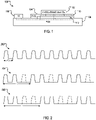
- the period T1 of timing diagram 206 may define a resonance frequency.
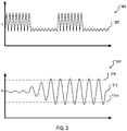
- the period of the resulting load current in the timing diagram 302 may be measured to determine a resonance frequency.
- the parameter value may be a vector that describes a prohibited application pattern of an operation that causes resonance. For example, with reference to Fig.
- precluding application of performance operations in a manner that causes a failure condition to occur may include monitoring, during application of performance operations, a period of a signal resulting from the application of the performance operation.
- a period of the application of the performance operation is adjusted so the periods no longer match. In other words, a signal with a certain periodicity may be avoided to preclude resonance.
- the signal that is monitored may be, for example, a clock signal, or a corresponding load signal.
- a computer storage medium can be, or be included in, a computer-readable storage device, a computer-readable storage substrate, a random or serial access memory array or device, or a combination of one or more of them.
- a computer storage medium is not a propagated signal, a computer storage medium can be a source or destination of computer program instructions encoded in an artificially-generated propagated signal.
- the computer storage medium can also be, or be included in, one or more separate physical components or media (e.g., multiple CDs, disks, or other storage devices).
- the processes and logic flows described in this specification can be performed by one or more programmable processors executing one or more computer programs to perform actions by operating on input data and generating output.
- the processes and logic flows can also be performed by, and apparatus can also be implemented as, special purpose logic circuitry, e.g., a FPGA (field programmable gate array) or an ASIC (application-specific integrated circuit).
- special purpose logic circuitry e.g., a FPGA (field programmable gate array) or an ASIC (application-specific integrated circuit).
Landscapes
- Engineering & Computer Science (AREA)
- Theoretical Computer Science (AREA)
- Physics & Mathematics (AREA)
- General Engineering & Computer Science (AREA)
- General Physics & Mathematics (AREA)
- Computer Networks & Wireless Communication (AREA)
- Signal Processing (AREA)
- Power Sources (AREA)
- Control Of Electric Motors In General (AREA)
- Electron Tubes For Measurement (AREA)
- Liquid Crystal Substances (AREA)
Priority Applications (2)
| Application Number | Priority Date | Filing Date | Title |
|---|---|---|---|
| DK22189521.2T DK4109845T3 (da) | 2019-05-09 | 2019-11-08 | Resonansbevist præstationsstyring |
| EP22189521.2A EP4109845B1 (en) | 2019-05-09 | 2019-11-08 | Resonance aware performance management |
Applications Claiming Priority (1)
| Application Number | Priority Date | Filing Date | Title |
|---|---|---|---|
| US16/408,088 US11054891B2 (en) | 2019-05-09 | 2019-05-09 | Resonance aware performance management |
Related Child Applications (2)
| Application Number | Title | Priority Date | Filing Date |
|---|---|---|---|
| EP22189521.2A Division-Into EP4109845B1 (en) | 2019-05-09 | 2019-11-08 | Resonance aware performance management |
| EP22189521.2A Division EP4109845B1 (en) | 2019-05-09 | 2019-11-08 | Resonance aware performance management |
Publications (2)
| Publication Number | Publication Date |
|---|---|
| EP3737041A1 EP3737041A1 (en) | 2020-11-11 |
| EP3737041B1 true EP3737041B1 (en) | 2022-09-14 |
Family
ID=68501373
Family Applications (2)
| Application Number | Title | Priority Date | Filing Date |
|---|---|---|---|
| EP19207892.1A Active EP3737041B1 (en) | 2019-05-09 | 2019-11-08 | Resonance aware performance management |
| EP22189521.2A Active EP4109845B1 (en) | 2019-05-09 | 2019-11-08 | Resonance aware performance management |
Family Applications After (1)
| Application Number | Title | Priority Date | Filing Date |
|---|---|---|---|
| EP22189521.2A Active EP4109845B1 (en) | 2019-05-09 | 2019-11-08 | Resonance aware performance management |
Country Status (4)
| Country | Link |
|---|---|
| US (2) | US11054891B2 (da) |
| EP (2) | EP3737041B1 (da) |
| DK (2) | DK3737041T3 (da) |
| FI (2) | FI4109845T3 (da) |
Families Citing this family (2)
| Publication number | Priority date | Publication date | Assignee | Title |
|---|---|---|---|---|
| US12494638B2 (en) | 2022-10-28 | 2025-12-09 | Nxp Usa, Inc. | System and method of controlling communication interface to avoid power distribution resonance conflict |
| US12386382B2 (en) * | 2023-06-05 | 2025-08-12 | Qualcomm Incorporated | Reduced training for main band chip module interconnection clock lines |
Family Cites Families (19)
| Publication number | Priority date | Publication date | Assignee | Title |
|---|---|---|---|---|
| JP2901649B2 (ja) * | 1989-07-31 | 1999-06-07 | 株式会社日立製作所 | 半導体装置及びそれを用いたカメラ |
| US5625550A (en) * | 1994-09-27 | 1997-04-29 | Allen-Bradley Company, Inc. | Apparatus used with AC motors for compensating for turn on delay errors |
| FR2811824B1 (fr) * | 2000-07-17 | 2002-10-18 | Sagem | Moteur electrique a deux modes de communication d'alimentation |
| US20070255547A1 (en) * | 2006-04-04 | 2007-11-01 | Xpedion Design Systems, Inc. | Solving the periodic steady-state operating condition of a phase-locked loop or delay-locked loop circuit using a transient estimation method |
| WO2013032753A2 (en) | 2011-08-26 | 2013-03-07 | The Trustees Of Columbia University In The City Of New York | Systems and methods for switched-inductor integrated voltage regulators |
| US8513974B1 (en) | 2012-01-17 | 2013-08-20 | Altera Corporation | Power distribution network noise reduction |
| CN104169879B (zh) * | 2012-04-24 | 2019-01-04 | 英特尔公司 | 用于动态中断重新配置的方法和计算机系统 |
| US9903916B2 (en) | 2012-09-27 | 2018-02-27 | Nxp Usa, Inc. | Scan test system with a test interface having a clock control unit for stretching a power shift cycle |
| US9100047B2 (en) | 2013-09-20 | 2015-08-04 | Intel Corporation | Method and apparatus for mitigating resonant effects within a power delivery network of a printed circuit board |
| DE102014218530B4 (de) * | 2014-09-16 | 2024-11-14 | Siemens Healthineers Ag | Verfahren zum Betrieb einer Magnetresonanzeinrichtung, Magnetresonanzeinrichtung und Computerprogramm |
| US9811143B2 (en) * | 2014-12-23 | 2017-11-07 | Intel Corporation | Systems and methods for dynamic spatial power steering |
| US9778676B2 (en) | 2015-08-03 | 2017-10-03 | Qualcomm Incorporated | Power distribution network (PDN) droop/overshoot mitigation in dynamic frequency scaling |
| US10496141B2 (en) * | 2016-03-17 | 2019-12-03 | Qualcomm Incorporated | System and method for intelligent thermal management in a system on a chip having a heterogeneous cluster architecture |
| US10340123B2 (en) * | 2016-05-26 | 2019-07-02 | Tokyo Electron Limited | Multi-frequency power modulation for etching high aspect ratio features |
| US10310572B2 (en) * | 2016-06-10 | 2019-06-04 | Microsoft Technology Licensing, Llc | Voltage based thermal control of processing device |
| US10009016B1 (en) | 2016-12-28 | 2018-06-26 | Qualcomm Incorporated | Dynamically adaptive voltage-frequency guardband control circuit |
| US10423204B2 (en) * | 2017-03-15 | 2019-09-24 | International Business Machines Corporation | Enforcing power caps on computing devices with multiple power feeds |
| US11080095B2 (en) * | 2017-06-04 | 2021-08-03 | Apple Inc. | Scheduling of work interval objects in an AMP architecture using a closed loop performance controller |
| US11126232B2 (en) * | 2018-11-28 | 2021-09-21 | Intel Corporation | Battery heat balancing during peak power mode |
-
2019
- 2019-05-09 US US16/408,088 patent/US11054891B2/en active Active
- 2019-11-08 DK DK19207892.1T patent/DK3737041T3/da active
- 2019-11-08 EP EP19207892.1A patent/EP3737041B1/en active Active
- 2019-11-08 FI FIEP22189521.2T patent/FI4109845T3/fi active
- 2019-11-08 FI FIEP19207892.1T patent/FI3737041T3/fi active
- 2019-11-08 EP EP22189521.2A patent/EP4109845B1/en active Active
- 2019-11-08 DK DK22189521.2T patent/DK4109845T3/da active
-
2021
- 2021-06-07 US US17/340,878 patent/US11435818B2/en active Active
Also Published As
| Publication number | Publication date |
|---|---|
| US20200356158A1 (en) | 2020-11-12 |
| FI4109845T3 (fi) | 2026-04-01 |
| EP4109845B1 (en) | 2026-02-11 |
| DK3737041T3 (da) | 2022-12-05 |
| EP3737041A1 (en) | 2020-11-11 |
| US11054891B2 (en) | 2021-07-06 |
| US20210294411A1 (en) | 2021-09-23 |
| FI3737041T3 (fi) | 2022-12-15 |
| DK4109845T3 (da) | 2026-03-30 |
| EP4109845A1 (en) | 2022-12-28 |
| US11435818B2 (en) | 2022-09-06 |
Similar Documents
| Publication | Publication Date | Title |
|---|---|---|
| US7142996B2 (en) | Operating voltage determination for an integrated circuit | |
| US9348346B2 (en) | Voltage regulation subsystem | |
| US11435818B2 (en) | Resonance aware performance management | |
| US9342123B2 (en) | Determine voltage supplied to a core | |
| US20160033611A1 (en) | Systems And Methods Of Current Sense Calibration For Voltage Regulator Circuits | |
| CN112732498B (zh) | 模拟设备单点上下电的测试方法、装置、设备及存储介质 | |
| US7610531B2 (en) | Modifying a test pattern to control power supply noise | |
| US8829712B2 (en) | Method and apparatus for controlling a supply current for a circuit or a plurality of circuit blocks | |
| US20230238800A1 (en) | Systems, devices and methods for power management and power estimation | |
| US11360827B2 (en) | Regulating core and un-core processor frequencies of computing node clusters | |
| US6842712B2 (en) | Method for testing an electronic component; computer program product, computer readable medium, and computer embodying the method; and method for downloading the program embodying the method | |
| US20080307282A1 (en) | System and Method for Electronic Device Development | |
| US7694163B1 (en) | System for generating and monitoring voltages generated for a variety of different components on a common printed circuit board | |
| US20050213268A1 (en) | Method and circuit for improving device power up timing and predictability | |
| TWI810984B (zh) | 電源時序控制系統及具有其之電子裝置 | |
| US6715135B2 (en) | Formal verification method | |
| US7321482B2 (en) | Sub-circuit voltage manipulation | |
| TWI819608B (zh) | 具有電源穩定測試機制的多核處理電路及其測試方法 | |
| EP0293261A2 (en) | Digital in-circuit tester having channel-memory erase-preventer | |
| US20230420068A1 (en) | Semiconductor test apparatus capable of inducing reduction of power consumption | |
| CN117174155A (zh) | 具有电源稳定测试机制的多核处理电路及其测试方法 | |
| JP7083728B2 (ja) | 自己診断装置、半導体装置及び自己診断方法 | |
| EP0293260A2 (en) | Digital in-circuit tester having a channel-driver inhibitor | |
| US20210074321A1 (en) | Manufacturing method of magnetic disk device and magnetic disk device | |
| TWM682190U (zh) | 經組態以在半導體裝置測試期間偵測類比電訊號之安定之半導體測試設備及非暫時性電腦儲存媒體 |
Legal Events
| Date | Code | Title | Description |
|---|---|---|---|
| PUAI | Public reference made under article 153(3) epc to a published international application that has entered the european phase |
Free format text: ORIGINAL CODE: 0009012 |
|
| STAA | Information on the status of an ep patent application or granted ep patent |
Free format text: STATUS: REQUEST FOR EXAMINATION WAS MADE |
|
| 17P | Request for examination filed |
Effective date: 20191108 |
|
| AK | Designated contracting states |
Kind code of ref document: A1 Designated state(s): AL AT BE BG CH CY CZ DE DK EE ES FI FR GB GR HR HU IE IS IT LI LT LU LV MC MK MT NL NO PL PT RO RS SE SI SK SM TR |
|
| AX | Request for extension of the european patent |
Extension state: BA ME |
|
| REG | Reference to a national code |
Ref country code: DE Ref legal event code: R079 Ref document number: 602019019536 Country of ref document: DE Free format text: PREVIOUS MAIN CLASS: H04L0012260000 Ipc: H04L0041081600 |
|
| GRAP | Despatch of communication of intention to grant a patent |
Free format text: ORIGINAL CODE: EPIDOSNIGR1 |
|
| RIC1 | Information provided on ipc code assigned before grant |
Ipc: H04L 43/50 20220101ALI20220225BHEP Ipc: H04L 41/0833 20220101ALI20220225BHEP Ipc: H04L 41/0816 20220101AFI20220225BHEP |
|
| STAA | Information on the status of an ep patent application or granted ep patent |
Free format text: STATUS: GRANT OF PATENT IS INTENDED |
|
| INTG | Intention to grant announced |
Effective date: 20220407 |
|
| GRAS | Grant fee paid |
Free format text: ORIGINAL CODE: EPIDOSNIGR3 |
|
| GRAA | (expected) grant |
Free format text: ORIGINAL CODE: 0009210 |
|
| STAA | Information on the status of an ep patent application or granted ep patent |
Free format text: STATUS: THE PATENT HAS BEEN GRANTED |
|
| AK | Designated contracting states |
Kind code of ref document: B1 Designated state(s): AL AT BE BG CH CY CZ DE DK EE ES FI FR GB GR HR HU IE IS IT LI LT LU LV MC MK MT NL NO PL PT RO RS SE SI SK SM TR |
|
| REG | Reference to a national code |
Ref country code: GB Ref legal event code: FG4D |
|
| REG | Reference to a national code |
Ref country code: CH Ref legal event code: EP |
|
| REG | Reference to a national code |
Ref country code: DE Ref legal event code: R096 Ref document number: 602019019536 Country of ref document: DE |
|
| REG | Reference to a national code |
Ref country code: IE Ref legal event code: FG4D |
|
| REG | Reference to a national code |
Ref country code: AT Ref legal event code: REF Ref document number: 1519374 Country of ref document: AT Kind code of ref document: T Effective date: 20221015 |
|
| REG | Reference to a national code |
Ref country code: DK Ref legal event code: T3 Effective date: 20221129 |
|
| REG | Reference to a national code |
Ref country code: NL Ref legal event code: FP |
|
| REG | Reference to a national code |
Ref country code: SE Ref legal event code: TRGR |
|
| REG | Reference to a national code |
Ref country code: LT Ref legal event code: MG9D |
|
| PG25 | Lapsed in a contracting state [announced via postgrant information from national office to epo] |
Ref country code: RS Free format text: LAPSE BECAUSE OF FAILURE TO SUBMIT A TRANSLATION OF THE DESCRIPTION OR TO PAY THE FEE WITHIN THE PRESCRIBED TIME-LIMIT Effective date: 20220914 Ref country code: NO Free format text: LAPSE BECAUSE OF FAILURE TO SUBMIT A TRANSLATION OF THE DESCRIPTION OR TO PAY THE FEE WITHIN THE PRESCRIBED TIME-LIMIT Effective date: 20221214 Ref country code: LV Free format text: LAPSE BECAUSE OF FAILURE TO SUBMIT A TRANSLATION OF THE DESCRIPTION OR TO PAY THE FEE WITHIN THE PRESCRIBED TIME-LIMIT Effective date: 20220914 Ref country code: LT Free format text: LAPSE BECAUSE OF FAILURE TO SUBMIT A TRANSLATION OF THE DESCRIPTION OR TO PAY THE FEE WITHIN THE PRESCRIBED TIME-LIMIT Effective date: 20220914 |
|
| REG | Reference to a national code |
Ref country code: AT Ref legal event code: MK05 Ref document number: 1519374 Country of ref document: AT Kind code of ref document: T Effective date: 20220914 |
|
| PG25 | Lapsed in a contracting state [announced via postgrant information from national office to epo] |
Ref country code: HR Free format text: LAPSE BECAUSE OF FAILURE TO SUBMIT A TRANSLATION OF THE DESCRIPTION OR TO PAY THE FEE WITHIN THE PRESCRIBED TIME-LIMIT Effective date: 20220914 Ref country code: GR Free format text: LAPSE BECAUSE OF FAILURE TO SUBMIT A TRANSLATION OF THE DESCRIPTION OR TO PAY THE FEE WITHIN THE PRESCRIBED TIME-LIMIT Effective date: 20221215 |
|
| PG25 | Lapsed in a contracting state [announced via postgrant information from national office to epo] |
Ref country code: SM Free format text: LAPSE BECAUSE OF FAILURE TO SUBMIT A TRANSLATION OF THE DESCRIPTION OR TO PAY THE FEE WITHIN THE PRESCRIBED TIME-LIMIT Effective date: 20220914 Ref country code: RO Free format text: LAPSE BECAUSE OF FAILURE TO SUBMIT A TRANSLATION OF THE DESCRIPTION OR TO PAY THE FEE WITHIN THE PRESCRIBED TIME-LIMIT Effective date: 20220914 Ref country code: PT Free format text: LAPSE BECAUSE OF FAILURE TO SUBMIT A TRANSLATION OF THE DESCRIPTION OR TO PAY THE FEE WITHIN THE PRESCRIBED TIME-LIMIT Effective date: 20230116 Ref country code: ES Free format text: LAPSE BECAUSE OF FAILURE TO SUBMIT A TRANSLATION OF THE DESCRIPTION OR TO PAY THE FEE WITHIN THE PRESCRIBED TIME-LIMIT Effective date: 20220914 Ref country code: CZ Free format text: LAPSE BECAUSE OF FAILURE TO SUBMIT A TRANSLATION OF THE DESCRIPTION OR TO PAY THE FEE WITHIN THE PRESCRIBED TIME-LIMIT Effective date: 20220914 Ref country code: AT Free format text: LAPSE BECAUSE OF FAILURE TO SUBMIT A TRANSLATION OF THE DESCRIPTION OR TO PAY THE FEE WITHIN THE PRESCRIBED TIME-LIMIT Effective date: 20220914 |
|
| PG25 | Lapsed in a contracting state [announced via postgrant information from national office to epo] |
Ref country code: SK Free format text: LAPSE BECAUSE OF FAILURE TO SUBMIT A TRANSLATION OF THE DESCRIPTION OR TO PAY THE FEE WITHIN THE PRESCRIBED TIME-LIMIT Effective date: 20220914 Ref country code: PL Free format text: LAPSE BECAUSE OF FAILURE TO SUBMIT A TRANSLATION OF THE DESCRIPTION OR TO PAY THE FEE WITHIN THE PRESCRIBED TIME-LIMIT Effective date: 20220914 Ref country code: IS Free format text: LAPSE BECAUSE OF FAILURE TO SUBMIT A TRANSLATION OF THE DESCRIPTION OR TO PAY THE FEE WITHIN THE PRESCRIBED TIME-LIMIT Effective date: 20230114 Ref country code: EE Free format text: LAPSE BECAUSE OF FAILURE TO SUBMIT A TRANSLATION OF THE DESCRIPTION OR TO PAY THE FEE WITHIN THE PRESCRIBED TIME-LIMIT Effective date: 20220914 |
|
| P01 | Opt-out of the competence of the unified patent court (upc) registered |
Effective date: 20230505 |
|
| REG | Reference to a national code |
Ref country code: DE Ref legal event code: R097 Ref document number: 602019019536 Country of ref document: DE |
|
| PG25 | Lapsed in a contracting state [announced via postgrant information from national office to epo] |
Ref country code: MC Free format text: LAPSE BECAUSE OF FAILURE TO SUBMIT A TRANSLATION OF THE DESCRIPTION OR TO PAY THE FEE WITHIN THE PRESCRIBED TIME-LIMIT Effective date: 20220914 Ref country code: AL Free format text: LAPSE BECAUSE OF FAILURE TO SUBMIT A TRANSLATION OF THE DESCRIPTION OR TO PAY THE FEE WITHIN THE PRESCRIBED TIME-LIMIT Effective date: 20220914 |
|
| PLBE | No opposition filed within time limit |
Free format text: ORIGINAL CODE: 0009261 |
|
| STAA | Information on the status of an ep patent application or granted ep patent |
Free format text: STATUS: NO OPPOSITION FILED WITHIN TIME LIMIT |
|
| 26N | No opposition filed |
Effective date: 20230615 |
|
| PG25 | Lapsed in a contracting state [announced via postgrant information from national office to epo] |
Ref country code: SI Free format text: LAPSE BECAUSE OF FAILURE TO SUBMIT A TRANSLATION OF THE DESCRIPTION OR TO PAY THE FEE WITHIN THE PRESCRIBED TIME-LIMIT Effective date: 20220914 Ref country code: LU Free format text: LAPSE BECAUSE OF NON-PAYMENT OF DUE FEES Effective date: 20221108 |
|
| PG25 | Lapsed in a contracting state [announced via postgrant information from national office to epo] |
Ref country code: CY Free format text: LAPSE BECAUSE OF FAILURE TO SUBMIT A TRANSLATION OF THE DESCRIPTION OR TO PAY THE FEE WITHIN THE PRESCRIBED TIME-LIMIT Effective date: 20220914 |
|
| PG25 | Lapsed in a contracting state [announced via postgrant information from national office to epo] |
Ref country code: MK Free format text: LAPSE BECAUSE OF FAILURE TO SUBMIT A TRANSLATION OF THE DESCRIPTION OR TO PAY THE FEE WITHIN THE PRESCRIBED TIME-LIMIT Effective date: 20220914 Ref country code: IT Free format text: LAPSE BECAUSE OF FAILURE TO SUBMIT A TRANSLATION OF THE DESCRIPTION OR TO PAY THE FEE WITHIN THE PRESCRIBED TIME-LIMIT Effective date: 20220914 Ref country code: HU Free format text: LAPSE BECAUSE OF FAILURE TO SUBMIT A TRANSLATION OF THE DESCRIPTION OR TO PAY THE FEE WITHIN THE PRESCRIBED TIME-LIMIT; INVALID AB INITIO Effective date: 20191108 |
|
| PG25 | Lapsed in a contracting state [announced via postgrant information from national office to epo] |
Ref country code: TR Free format text: LAPSE BECAUSE OF FAILURE TO SUBMIT A TRANSLATION OF THE DESCRIPTION OR TO PAY THE FEE WITHIN THE PRESCRIBED TIME-LIMIT Effective date: 20220914 |
|
| PG25 | Lapsed in a contracting state [announced via postgrant information from national office to epo] |
Ref country code: BG Free format text: LAPSE BECAUSE OF FAILURE TO SUBMIT A TRANSLATION OF THE DESCRIPTION OR TO PAY THE FEE WITHIN THE PRESCRIBED TIME-LIMIT Effective date: 20220914 |
|
| PG25 | Lapsed in a contracting state [announced via postgrant information from national office to epo] |
Ref country code: MT Free format text: LAPSE BECAUSE OF FAILURE TO SUBMIT A TRANSLATION OF THE DESCRIPTION OR TO PAY THE FEE WITHIN THE PRESCRIBED TIME-LIMIT Effective date: 20220914 |
|
| REG | Reference to a national code |
Ref country code: CH Ref legal event code: U11 Free format text: ST27 STATUS EVENT CODE: U-0-0-U10-U11 (AS PROVIDED BY THE NATIONAL OFFICE) Effective date: 20251201 |
|
| PGFP | Annual fee paid to national office [announced via postgrant information from national office to epo] |
Ref country code: NL Payment date: 20251126 Year of fee payment: 7 |
|
| PGFP | Annual fee paid to national office [announced via postgrant information from national office to epo] |
Ref country code: DE Payment date: 20251128 Year of fee payment: 7 |
|
| PGFP | Annual fee paid to national office [announced via postgrant information from national office to epo] |
Ref country code: GB Payment date: 20251127 Year of fee payment: 7 |
|
| PGFP | Annual fee paid to national office [announced via postgrant information from national office to epo] |
Ref country code: FI Payment date: 20251125 Year of fee payment: 7 Ref country code: DK Payment date: 20251125 Year of fee payment: 7 |
|
| PGFP | Annual fee paid to national office [announced via postgrant information from national office to epo] |
Ref country code: FR Payment date: 20251125 Year of fee payment: 7 |
|
| PGFP | Annual fee paid to national office [announced via postgrant information from national office to epo] |
Ref country code: BE Payment date: 20251127 Year of fee payment: 7 |
|
| PGFP | Annual fee paid to national office [announced via postgrant information from national office to epo] |
Ref country code: CH Payment date: 20251201 Year of fee payment: 7 Ref country code: SE Payment date: 20251127 Year of fee payment: 7 |
|
| PGFP | Annual fee paid to national office [announced via postgrant information from national office to epo] |
Ref country code: IE Payment date: 20251127 Year of fee payment: 7 |