EP3736620A1 - Hintergrundbeleuchtungsquelle, herstellungsverfahren dafür und anzeigevorrichtung - Google Patents
Hintergrundbeleuchtungsquelle, herstellungsverfahren dafür und anzeigevorrichtung Download PDFInfo
- Publication number
- EP3736620A1 EP3736620A1 EP18889972.8A EP18889972A EP3736620A1 EP 3736620 A1 EP3736620 A1 EP 3736620A1 EP 18889972 A EP18889972 A EP 18889972A EP 3736620 A1 EP3736620 A1 EP 3736620A1
- Authority
- EP
- European Patent Office
- Prior art keywords
- light
- guide plate
- light guide
- layer
- emitting device
- Prior art date
- Legal status (The legal status is an assumption and is not a legal conclusion. Google has not performed a legal analysis and makes no representation as to the accuracy of the status listed.)
- Withdrawn
Links
- 238000004519 manufacturing process Methods 0.000 title claims abstract description 18
- 230000003287 optical effect Effects 0.000 claims abstract description 101
- 230000001902 propagating effect Effects 0.000 claims abstract description 16
- 230000008878 coupling Effects 0.000 claims description 67
- 238000010168 coupling process Methods 0.000 claims description 67
- 238000005859 coupling reaction Methods 0.000 claims description 67
- 239000004973 liquid crystal related substance Substances 0.000 claims description 51
- 238000006243 chemical reaction Methods 0.000 claims description 50
- 239000000463 material Substances 0.000 claims description 42
- 230000000903 blocking effect Effects 0.000 claims description 18
- 230000000875 corresponding effect Effects 0.000 claims description 18
- 238000000034 method Methods 0.000 claims description 14
- 239000000758 substrate Substances 0.000 claims description 14
- 230000010287 polarization Effects 0.000 claims description 12
- 239000012780 transparent material Substances 0.000 claims description 5
- 230000001419 dependent effect Effects 0.000 claims description 4
- 230000005540 biological transmission Effects 0.000 claims description 3
- 230000002596 correlated effect Effects 0.000 claims description 3
- CNQCVBJFEGMYDW-UHFFFAOYSA-N lawrencium atom Chemical compound [Lr] CNQCVBJFEGMYDW-UHFFFAOYSA-N 0.000 description 64
- 238000010586 diagram Methods 0.000 description 14
- 238000004422 calculation algorithm Methods 0.000 description 11
- 230000005684 electric field Effects 0.000 description 7
- 230000008569 process Effects 0.000 description 7
- 238000009826 distribution Methods 0.000 description 5
- 239000011347 resin Substances 0.000 description 5
- 229920005989 resin Polymers 0.000 description 5
- 239000000853 adhesive Substances 0.000 description 4
- 230000001070 adhesive effect Effects 0.000 description 4
- 239000003086 colorant Substances 0.000 description 4
- 239000010408 film Substances 0.000 description 4
- 238000005457 optimization Methods 0.000 description 4
- 229920002120 photoresistant polymer Polymers 0.000 description 4
- 230000001276 controlling effect Effects 0.000 description 3
- 230000000694 effects Effects 0.000 description 3
- 238000005530 etching Methods 0.000 description 3
- 229910052581 Si3N4 Inorganic materials 0.000 description 2
- VYPSYNLAJGMNEJ-UHFFFAOYSA-N Silicium dioxide Chemical compound O=[Si]=O VYPSYNLAJGMNEJ-UHFFFAOYSA-N 0.000 description 2
- 238000000151 deposition Methods 0.000 description 2
- 238000012938 design process Methods 0.000 description 2
- 238000004049 embossing Methods 0.000 description 2
- 239000011521 glass Substances 0.000 description 2
- HQVNEWCFYHHQES-UHFFFAOYSA-N silicon nitride Chemical compound N12[Si]34N5[Si]62N3[Si]51N64 HQVNEWCFYHHQES-UHFFFAOYSA-N 0.000 description 2
- 229910052814 silicon oxide Inorganic materials 0.000 description 2
- 239000010409 thin film Substances 0.000 description 2
- 238000002834 transmittance Methods 0.000 description 2
- 241001270131 Agaricus moelleri Species 0.000 description 1
- -1 and A10 Chemical compound 0.000 description 1
- 230000015572 biosynthetic process Effects 0.000 description 1
- 210000004027 cell Anatomy 0.000 description 1
- 230000000295 complement effect Effects 0.000 description 1
- 210000002858 crystal cell Anatomy 0.000 description 1
- 230000007812 deficiency Effects 0.000 description 1
- 238000011161 development Methods 0.000 description 1
- 230000009189 diving Effects 0.000 description 1
- 230000002068 genetic effect Effects 0.000 description 1
- 238000001093 holography Methods 0.000 description 1
- AMGQUBHHOARCQH-UHFFFAOYSA-N indium;oxotin Chemical compound [In].[Sn]=O AMGQUBHHOARCQH-UHFFFAOYSA-N 0.000 description 1
- 230000031700 light absorption Effects 0.000 description 1
- 239000011159 matrix material Substances 0.000 description 1
- 229910052751 metal Inorganic materials 0.000 description 1
- 239000002184 metal Substances 0.000 description 1
- 238000012986 modification Methods 0.000 description 1
- 230000004048 modification Effects 0.000 description 1
- 238000002161 passivation Methods 0.000 description 1
- 238000002310 reflectometry Methods 0.000 description 1
- 230000008439 repair process Effects 0.000 description 1
- 230000004044 response Effects 0.000 description 1
- 239000004065 semiconductor Substances 0.000 description 1
- 238000002922 simulated annealing Methods 0.000 description 1
- 238000001228 spectrum Methods 0.000 description 1
- 238000006467 substitution reaction Methods 0.000 description 1
- 238000012876 topography Methods 0.000 description 1
Images
Classifications
-
- G—PHYSICS
- G02—OPTICS
- G02F—OPTICAL DEVICES OR ARRANGEMENTS FOR THE CONTROL OF LIGHT BY MODIFICATION OF THE OPTICAL PROPERTIES OF THE MEDIA OF THE ELEMENTS INVOLVED THEREIN; NON-LINEAR OPTICS; FREQUENCY-CHANGING OF LIGHT; OPTICAL LOGIC ELEMENTS; OPTICAL ANALOGUE/DIGITAL CONVERTERS
- G02F1/00—Devices or arrangements for the control of the intensity, colour, phase, polarisation or direction of light arriving from an independent light source, e.g. switching, gating or modulating; Non-linear optics
- G02F1/01—Devices or arrangements for the control of the intensity, colour, phase, polarisation or direction of light arriving from an independent light source, e.g. switching, gating or modulating; Non-linear optics for the control of the intensity, phase, polarisation or colour
- G02F1/19—Devices or arrangements for the control of the intensity, colour, phase, polarisation or direction of light arriving from an independent light source, e.g. switching, gating or modulating; Non-linear optics for the control of the intensity, phase, polarisation or colour based on variable-reflection or variable-refraction elements not provided for in groups G02F1/015 - G02F1/169
-
- G—PHYSICS
- G02—OPTICS
- G02B—OPTICAL ELEMENTS, SYSTEMS OR APPARATUS
- G02B6/00—Light guides; Structural details of arrangements comprising light guides and other optical elements, e.g. couplings
- G02B6/0001—Light guides; Structural details of arrangements comprising light guides and other optical elements, e.g. couplings specially adapted for lighting devices or systems
- G02B6/0011—Light guides; Structural details of arrangements comprising light guides and other optical elements, e.g. couplings specially adapted for lighting devices or systems the light guides being planar or of plate-like form
- G02B6/0033—Means for improving the coupling-out of light from the light guide
- G02B6/005—Means for improving the coupling-out of light from the light guide provided by one optical element, or plurality thereof, placed on the light output side of the light guide
-
- G—PHYSICS
- G02—OPTICS
- G02B—OPTICAL ELEMENTS, SYSTEMS OR APPARATUS
- G02B6/00—Light guides; Structural details of arrangements comprising light guides and other optical elements, e.g. couplings
- G02B6/0001—Light guides; Structural details of arrangements comprising light guides and other optical elements, e.g. couplings specially adapted for lighting devices or systems
- G02B6/0011—Light guides; Structural details of arrangements comprising light guides and other optical elements, e.g. couplings specially adapted for lighting devices or systems the light guides being planar or of plate-like form
- G02B6/0033—Means for improving the coupling-out of light from the light guide
- G02B6/005—Means for improving the coupling-out of light from the light guide provided by one optical element, or plurality thereof, placed on the light output side of the light guide
- G02B6/0055—Reflecting element, sheet or layer
-
- G—PHYSICS
- G02—OPTICS
- G02B—OPTICAL ELEMENTS, SYSTEMS OR APPARATUS
- G02B6/00—Light guides; Structural details of arrangements comprising light guides and other optical elements, e.g. couplings
- G02B6/0001—Light guides; Structural details of arrangements comprising light guides and other optical elements, e.g. couplings specially adapted for lighting devices or systems
- G02B6/0011—Light guides; Structural details of arrangements comprising light guides and other optical elements, e.g. couplings specially adapted for lighting devices or systems the light guides being planar or of plate-like form
- G02B6/0033—Means for improving the coupling-out of light from the light guide
- G02B6/005—Means for improving the coupling-out of light from the light guide provided by one optical element, or plurality thereof, placed on the light output side of the light guide
- G02B6/0051—Diffusing sheet or layer
-
- G—PHYSICS
- G02—OPTICS
- G02B—OPTICAL ELEMENTS, SYSTEMS OR APPARATUS
- G02B6/00—Light guides; Structural details of arrangements comprising light guides and other optical elements, e.g. couplings
- G02B6/0001—Light guides; Structural details of arrangements comprising light guides and other optical elements, e.g. couplings specially adapted for lighting devices or systems
- G02B6/0011—Light guides; Structural details of arrangements comprising light guides and other optical elements, e.g. couplings specially adapted for lighting devices or systems the light guides being planar or of plate-like form
- G02B6/0033—Means for improving the coupling-out of light from the light guide
- G02B6/0056—Means for improving the coupling-out of light from the light guide for producing polarisation effects, e.g. by a surface with polarizing properties or by an additional polarizing elements
-
- G—PHYSICS
- G02—OPTICS
- G02F—OPTICAL DEVICES OR ARRANGEMENTS FOR THE CONTROL OF LIGHT BY MODIFICATION OF THE OPTICAL PROPERTIES OF THE MEDIA OF THE ELEMENTS INVOLVED THEREIN; NON-LINEAR OPTICS; FREQUENCY-CHANGING OF LIGHT; OPTICAL LOGIC ELEMENTS; OPTICAL ANALOGUE/DIGITAL CONVERTERS
- G02F1/00—Devices or arrangements for the control of the intensity, colour, phase, polarisation or direction of light arriving from an independent light source, e.g. switching, gating or modulating; Non-linear optics
- G02F1/01—Devices or arrangements for the control of the intensity, colour, phase, polarisation or direction of light arriving from an independent light source, e.g. switching, gating or modulating; Non-linear optics for the control of the intensity, phase, polarisation or colour
- G02F1/13—Devices or arrangements for the control of the intensity, colour, phase, polarisation or direction of light arriving from an independent light source, e.g. switching, gating or modulating; Non-linear optics for the control of the intensity, phase, polarisation or colour based on liquid crystals, e.g. single liquid crystal display cells
- G02F1/133—Constructional arrangements; Operation of liquid crystal cells; Circuit arrangements
- G02F1/1333—Constructional arrangements; Manufacturing methods
- G02F1/1335—Structural association of cells with optical devices, e.g. polarisers or reflectors
- G02F1/133504—Diffusing, scattering, diffracting elements
-
- G—PHYSICS
- G02—OPTICS
- G02F—OPTICAL DEVICES OR ARRANGEMENTS FOR THE CONTROL OF LIGHT BY MODIFICATION OF THE OPTICAL PROPERTIES OF THE MEDIA OF THE ELEMENTS INVOLVED THEREIN; NON-LINEAR OPTICS; FREQUENCY-CHANGING OF LIGHT; OPTICAL LOGIC ELEMENTS; OPTICAL ANALOGUE/DIGITAL CONVERTERS
- G02F1/00—Devices or arrangements for the control of the intensity, colour, phase, polarisation or direction of light arriving from an independent light source, e.g. switching, gating or modulating; Non-linear optics
- G02F1/01—Devices or arrangements for the control of the intensity, colour, phase, polarisation or direction of light arriving from an independent light source, e.g. switching, gating or modulating; Non-linear optics for the control of the intensity, phase, polarisation or colour
- G02F1/13—Devices or arrangements for the control of the intensity, colour, phase, polarisation or direction of light arriving from an independent light source, e.g. switching, gating or modulating; Non-linear optics for the control of the intensity, phase, polarisation or colour based on liquid crystals, e.g. single liquid crystal display cells
- G02F1/133—Constructional arrangements; Operation of liquid crystal cells; Circuit arrangements
- G02F1/1333—Constructional arrangements; Manufacturing methods
- G02F1/1335—Structural association of cells with optical devices, e.g. polarisers or reflectors
- G02F1/1336—Illuminating devices
- G02F1/133602—Direct backlight
- G02F1/133606—Direct backlight including a specially adapted diffusing, scattering or light controlling members
-
- G—PHYSICS
- G02—OPTICS
- G02F—OPTICAL DEVICES OR ARRANGEMENTS FOR THE CONTROL OF LIGHT BY MODIFICATION OF THE OPTICAL PROPERTIES OF THE MEDIA OF THE ELEMENTS INVOLVED THEREIN; NON-LINEAR OPTICS; FREQUENCY-CHANGING OF LIGHT; OPTICAL LOGIC ELEMENTS; OPTICAL ANALOGUE/DIGITAL CONVERTERS
- G02F1/00—Devices or arrangements for the control of the intensity, colour, phase, polarisation or direction of light arriving from an independent light source, e.g. switching, gating or modulating; Non-linear optics
- G02F1/01—Devices or arrangements for the control of the intensity, colour, phase, polarisation or direction of light arriving from an independent light source, e.g. switching, gating or modulating; Non-linear optics for the control of the intensity, phase, polarisation or colour
- G02F1/13—Devices or arrangements for the control of the intensity, colour, phase, polarisation or direction of light arriving from an independent light source, e.g. switching, gating or modulating; Non-linear optics for the control of the intensity, phase, polarisation or colour based on liquid crystals, e.g. single liquid crystal display cells
- G02F1/133—Constructional arrangements; Operation of liquid crystal cells; Circuit arrangements
- G02F1/1333—Constructional arrangements; Manufacturing methods
- G02F1/1335—Structural association of cells with optical devices, e.g. polarisers or reflectors
- G02F1/1336—Illuminating devices
- G02F1/133615—Edge-illuminating devices, i.e. illuminating from the side
-
- G—PHYSICS
- G02—OPTICS
- G02F—OPTICAL DEVICES OR ARRANGEMENTS FOR THE CONTROL OF LIGHT BY MODIFICATION OF THE OPTICAL PROPERTIES OF THE MEDIA OF THE ELEMENTS INVOLVED THEREIN; NON-LINEAR OPTICS; FREQUENCY-CHANGING OF LIGHT; OPTICAL LOGIC ELEMENTS; OPTICAL ANALOGUE/DIGITAL CONVERTERS
- G02F1/00—Devices or arrangements for the control of the intensity, colour, phase, polarisation or direction of light arriving from an independent light source, e.g. switching, gating or modulating; Non-linear optics
- G02F1/01—Devices or arrangements for the control of the intensity, colour, phase, polarisation or direction of light arriving from an independent light source, e.g. switching, gating or modulating; Non-linear optics for the control of the intensity, phase, polarisation or colour
- G02F1/13—Devices or arrangements for the control of the intensity, colour, phase, polarisation or direction of light arriving from an independent light source, e.g. switching, gating or modulating; Non-linear optics for the control of the intensity, phase, polarisation or colour based on liquid crystals, e.g. single liquid crystal display cells
- G02F1/133—Constructional arrangements; Operation of liquid crystal cells; Circuit arrangements
- G02F1/1333—Constructional arrangements; Manufacturing methods
- G02F1/1335—Structural association of cells with optical devices, e.g. polarisers or reflectors
- G02F1/1336—Illuminating devices
- G02F1/133617—Illumination with ultraviolet light; Luminescent elements or materials associated to the cell
-
- G—PHYSICS
- G02—OPTICS
- G02F—OPTICAL DEVICES OR ARRANGEMENTS FOR THE CONTROL OF LIGHT BY MODIFICATION OF THE OPTICAL PROPERTIES OF THE MEDIA OF THE ELEMENTS INVOLVED THEREIN; NON-LINEAR OPTICS; FREQUENCY-CHANGING OF LIGHT; OPTICAL LOGIC ELEMENTS; OPTICAL ANALOGUE/DIGITAL CONVERTERS
- G02F1/00—Devices or arrangements for the control of the intensity, colour, phase, polarisation or direction of light arriving from an independent light source, e.g. switching, gating or modulating; Non-linear optics
- G02F1/29—Devices or arrangements for the control of the intensity, colour, phase, polarisation or direction of light arriving from an independent light source, e.g. switching, gating or modulating; Non-linear optics for the control of the position or the direction of light beams, i.e. deflection
- G02F1/292—Devices or arrangements for the control of the intensity, colour, phase, polarisation or direction of light arriving from an independent light source, e.g. switching, gating or modulating; Non-linear optics for the control of the position or the direction of light beams, i.e. deflection by controlled diffraction or phased-array beam steering
-
- G—PHYSICS
- G02—OPTICS
- G02B—OPTICAL ELEMENTS, SYSTEMS OR APPARATUS
- G02B6/00—Light guides; Structural details of arrangements comprising light guides and other optical elements, e.g. couplings
- G02B6/0001—Light guides; Structural details of arrangements comprising light guides and other optical elements, e.g. couplings specially adapted for lighting devices or systems
- G02B6/0011—Light guides; Structural details of arrangements comprising light guides and other optical elements, e.g. couplings specially adapted for lighting devices or systems the light guides being planar or of plate-like form
- G02B6/0013—Means for improving the coupling-in of light from the light source into the light guide
- G02B6/0015—Means for improving the coupling-in of light from the light source into the light guide provided on the surface of the light guide or in the bulk of it
- G02B6/0018—Redirecting means on the surface of the light guide
-
- G—PHYSICS
- G02—OPTICS
- G02B—OPTICAL ELEMENTS, SYSTEMS OR APPARATUS
- G02B6/00—Light guides; Structural details of arrangements comprising light guides and other optical elements, e.g. couplings
- G02B6/0001—Light guides; Structural details of arrangements comprising light guides and other optical elements, e.g. couplings specially adapted for lighting devices or systems
- G02B6/0011—Light guides; Structural details of arrangements comprising light guides and other optical elements, e.g. couplings specially adapted for lighting devices or systems the light guides being planar or of plate-like form
- G02B6/0013—Means for improving the coupling-in of light from the light source into the light guide
- G02B6/0023—Means for improving the coupling-in of light from the light source into the light guide provided by one optical element, or plurality thereof, placed between the light guide and the light source, or around the light source
- G02B6/0031—Reflecting element, sheet or layer
-
- G—PHYSICS
- G02—OPTICS
- G02B—OPTICAL ELEMENTS, SYSTEMS OR APPARATUS
- G02B6/00—Light guides; Structural details of arrangements comprising light guides and other optical elements, e.g. couplings
- G02B6/0001—Light guides; Structural details of arrangements comprising light guides and other optical elements, e.g. couplings specially adapted for lighting devices or systems
- G02B6/0011—Light guides; Structural details of arrangements comprising light guides and other optical elements, e.g. couplings specially adapted for lighting devices or systems the light guides being planar or of plate-like form
- G02B6/0033—Means for improving the coupling-out of light from the light guide
- G02B6/005—Means for improving the coupling-out of light from the light guide provided by one optical element, or plurality thereof, placed on the light output side of the light guide
- G02B6/0053—Prismatic sheet or layer; Brightness enhancement element, sheet or layer
Definitions
- the present disclosure relates to a backlight source, a method for manufacturing backlight source, and a display device
- the present disclosure provides a backlight source, a method for manufacturing backlight source, and a display device.
- the technical solutions are as follows:
- the backlight source comprises:
- a surface of the light guide plate comprises one or more coupling gratings; and each of the coupling gratings is configured to convert the parallel beam that is incident to be an emitting beam at a light intensity ratio corresponding to the position where the coupling grating is located, the exiting beam being a collimated beam propagating in a direction away from the light guide plate.
- a surface at the light emitting side of the light guide plate comprises one or more transmission coupling gratings, and a surface away from the light emitting side of the light guide plate comprises one or more reflection coupling gratings; and each of the coupling gratings is configured to convert the parallel beam that is incident to be an emitting beam at a light intensity ratio corresponding to the position where the coupling grating is located, the emitting beam being a collimated beam propagating in a direction away from the light guide plate.
- a surface of the light guide plate comprises a plurality of coupling gratings; a light intensity ratio that corresponds to the coupling gratings is positively correlated to a distance between the coupling gratings and the optical element; and each of the coupling gratings is configured to convert the parallel beam that is incident to be an exiting beam at a light intensity ratio corresponding to the position where the coupling grating is located, the exiting beam being a collimated beam propagating in a direction away from the light guide plate.
- the optical element is of a holographic microstructure that is polarization-dependent.
- the light guide plate is provided with a filling layer on both sides in the thickness direction, and a material refractive index of the light guide plate is greater than a material refractive index of the filling layer.
- the light guide plate and the filling layer are both formed of transparent material.
- the light emitting device is disposed at an edge of the light guide plate; the light guide plate is provided with a light absorbing layer on at least one side in the thickness direction; and the light absorbing layer is disposed at the edge of the light guide plate where the light emitting device is disposed.
- the light guide plate has a first side and a second side in the thickness direction; the light emitting device is disposed on a surface of the first side of the light guide plate; the optical element is disposed on a surface of the second side of the light guide plate; and the light emitting device and the optical element are disposed opposite to each other.
- a method for manufacturing a backlight source comprising:
- a display device comprising any of the backlight source above.
- the light conversion layer in each of the sub-pixels comprises a light transmissive region and a light blocking region, and the collimated beam provided by the backlight source for any of the sub-pixels is directed to the light blocking region of the sub-pixel.
- liquid crystal layer is configured to, under a bright-state bias voltage, deflect the collimated beam to be directed to the light transmissive region of the sub-pixel in which the collimated beam is located.
- the light emitting device is a blue light emitting device
- the light conversion layer comprises the light transmissive region that is red, the light transmissive region that is blue, and the light transmissive region that is green
- the light conversion layer in the light transmissive region that is red comprises a first photoluminescent material for converting blue light into red light
- the light conversion layer in the light transmissive region that is green comprises a second photoluminescent material for converting blue light into green light.
- a grating layer further comprising a grating layer, a liquid crystal layer and a light conversion layer that are sequentially stacked in a direction away from the backlight source, wherein the light conversion layer in each of the sub-pixels comprises a first region and a second region, and the collimated beam provided by the backlight source for any of the sub-pixels is directed to the first region of the sub-pixel; and the grating layer comprises deflection gratings in each of the sub-pixels, and each of the deflection gratings is configured to deflect the collimated beam to be directed to the second region of the sub-pixel in which the collimated beam is located; wherein the first region and the second region are respectively one of a light blocking region and a light transmissive region.
- the liquid crystal layer is configured to, under a dark-state bias voltage, have an edge refractive index that is same as a refractive index of a material for forming the grating layer; and the edge refractive index is a refractive index of the liquid crystal molecules that are close to the grating layer for the collimated beam.
- the light emitting device is a blue light emitting device
- the light conversion layer comprises the light transmissive region that is red, the light transmissive region that is blue, and the light transmissive region that is green
- the light conversion layer in the light transmissive region that is red comprises a first photoluminescent material that converts blue light to be red light
- the light conversion layer in the light transmissive region that is green comprises a second photoluminescent material that converts blue light to be green light.
- a buffer layer further comprising a buffer layer, a transistor device layer, a liquid crystal layer, a planarization layer, and a counter substrate, wherein the buffer layer, the transistor device layer, the liquid crystal layer, the planarization layer, the light conversion layer, and the counter substrate are sequentially disposed in a direction away from the backlight source.
- connection or “connected to” or a similar term is not limited to a physical or mechanical connection but may include an electrical connection that is direct or indirect.
- a typical edge-lit backlight source there is a light emitting device on a side surface of a light guide plate, and the light is coupled in the light guide plate from the side surface and then uniformly emitted from a light emitting surface of the light guide plate via a lens or a prism.
- an excessively thin light guide plate may make it difficult to attach the light emitting device to the side surface or may reduce the luminance of the light.
- the necessary optical auxiliary structures and supporting structures may increase the thickness of the backlight source, which makes it difficult to reduce the thickness of the backlight source and thereby fails to meet the application requirements of the liquid crystal display devices that are thin and light.
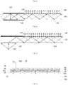
- FIG. 1 is a schematic diagram of a structure of a backlight source according to an example of the present disclosure.
- the backlight source includes a light guide plate 101, a light emitting device 102 and an optical element 103, may further include a filling layer 104, a light absorbing layer 105 and a coupling grating 106.
- the light guide plate 101 is horizontally placed in FIG. 1 , and the upper side and the lower side in FIG. 1 are respectively two sides of the light guide plate in the thickness direction.
- the position shown in FIG. 1 is an edge of the light guide plate 101, and the structure of remaining parts of the light guide plate 101 may be inferred from the structure shown in FIG. 1 .
- the light emitting device 102 is on an edge of the upper side of the light guide plate 101.
- the light emitting side of the light emitting device 102 faces downward, that is, towards the inside of the light guide plate 101.
- the light emitting device 102 is a light emitting diode (LED) chip that is embossed or attached to the light guide plate 101 on the edge of the upper surface.
- the light emitting device 102 is a thin-film light emitting device manufactured and formed at the edge of the upper surface of the light guide plate 101. Taking this as an example, the light emitting device 102 may emit light projected to the inside of the light guide plate 101.
- the optical element herein refers to a structure capable of realizing certain optical functions in a backlight source, which may be, for example, a surface structure that implements optical functions through a surface topography as included, a holographic microstructure (a microstructure achieving optical functions based on holography), or a structure consisting of prisms or lenses.
- the optical element 103 is on the light emitting side of the light emitting device 102 (that is, the optical element 103 is on the side where the light emitting device 102 emits light), and the relative position between the optical element 103 and the light emitting device 102 is fixed.
- the light emitting device 102 is a point light source and emits light in a conical shape.
- the shape, position and size of the optical element 103 may be set according to the pattern that is presented when the light emitted from the light emitting device 102 is irradiated onto the lower surface of the light guide plate 101.
- the optical element 103 is of a circular or elliptical shape centered on the axis of the cone (namely, the cone presented by the light emitted from the point light source), and can receive all of the light emitted from the light emitting device 102 to the lower surface of the light guide plate 101.
- the distance between the light emitting device 102 and the optical element 103 is the thickness h of the light guide plate 101.
- the light emitting device 102 and the optical element 103 are opposite to each other along the propagation direction of the light, so as to fix the relative position between the optical element 103 and the light emitting device 102.
- the optical element 103 may be provided within a range extended to the periphery, so that the range capable of receiving the light is larger than the range on which the light is practically irradiated. In this way, the deficiency in the manufacturing process at the edge or in the reliability of the microstructure at the edge may be prevented from affecting the light energy utilization rate of the optical element 103.
- the light emitting device 102 is a linear light source and emits light in a pyramid shape. At this time, the shape, position and size of the optical element 103 may also be set according to the pattern that is presented when the light emitted from the light emitting device 102 is irradiated onto the lower surface of the light guide plate 101.
- the optical element 103 is of a rectangle shape whose longitudinal direction coincides with the extending direction of the linear light source. Furthermore, the optical element 103 can receive all of the light emitted from the light emitting device 102 to the lower surface of the light guide plate 101. As such, the distance between the light emitting device 102 and the optical element 103 is the thickness h of the light guide plate 101. In addition, the light emitting device 102 and the optical element 103 are opposite to each other along the propagation direction of the light, so as to fix the relative position between the optical element 103 and the light emitting device 102.
- the optical element 103 is configured to reflect the light emitted from the light emitting device 102 to be a parallel beam that propagates in the light guide plate 101 by total reflection.
- the angle between the propagation direction of the parallel beam and the light guide plate 101 is a preset propagation angle ⁇ .
- the optical element 103 is designed in advance regarding the wavefront of the light emitted from the light emitting device 102 by a surface pattern that is of a minute structure and formed by, for example, embossing or etching the lower surface of the light guide plate 101.
- a surface pattern that is of a minute structure and formed by, for example, embossing or etching the lower surface of the light guide plate 101.
- parameters of the optical element 103 may be acquired by calculating by a simulation algorithm combined with a numerical optimization algorithm based on a modulation grating model, .
- the simulation algorithm may be, for example, a scalar theory, an angular spectrum theory, a rigorous coupled wave analysis (RCWA) algorithm, a finite difference time domain (FDTD) algorithm, a finite element (FEM) algorithm or the like;
- the numerical optimization algorithm may be, for example, a genetic algorithm, a simulated annealing algorithm, a Bee colony algorithm or the like. Values of the coefficients of respective powers may be calculated by the aforesaid manner according to the necessary information, such as, the wavelength of the light, the polarization state of the light, the refractive index of the medium on both sides, the incidence angle at different positions and the required reflection angle.
- the optical element 103 may reflect the light emitted from the light emitting device 102 to be a parallel beam having a preset propagation angle ⁇ inside the light guide plate 101.
- the optical element 103 is equivalent or approximately equivalent to a parabolic reflection surface having a focus at the light emitting device 102.
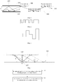
- the aforesaid modulation grating model may have the form shown in FIG. 2 or FIG. 3 in each grating period.
- FIG. 2 shows a grating structure formed by sequentially arranging a plurality of protrusions that have the same height, wherein the width of the protrusions and the interval between adjacent protrusions are modulatable, and optical structures having different functions may be obtained according to different modulation manners.
- FIG. 2 shows a grating structure formed by closely arranging a plurality of steps that have the same width, wherein the height of each step is modulatable, and optical structures having different functions may be obtained under different modulation modes.
- modulatable parameters in each grating period may be calculated and modulated according to the aforesaid design manner based on, for example, the modulation grating model shown in FIG. 2 or FIG. 3 , so as to obtain a grating structure that can convert the light emitted from the light emitting device 102 to be a parallel beam having a preset propagation angle ⁇ , and thereby dispose the grating structure on the light guide plate 101 as the optical element 103.
- the optical element 103 is polarization-dependent on the conversion of the light emitted from the light emitting device 102, so that the parallel beam converted by the optical element 103 may have a determined polarization state.
- the optical element 103 may have a strong response to and a high diffraction efficiency for the light in a certain polarization state, so that the wavefront of the light emitted from the light emitting device 102 may be efficiently converted to be the waveguide mode that the light propagates in the light guide plate 101 by a specific total reflection manner.
- the optical element 103 has a low diffraction efficiency for the light in other polarization states, and has substantially no effect as described above; and most of the light may be transmitted through the lower surface or the upper surface of the light guide plate 101.
- a light absorbing layer may be disposed on at least one side of the light guide plate 101 in the thickness direction.
- a light absorbing layer 105 is disposed at an edge, where the light emitting device 102 on the upper side and lower side is located respectively, of the light guide plate 101, so that the light that is not converted to be the parallel beam having the preset propagation angle ⁇ may be absorbed by the light absorbing layer 105.
- the light absorbing layer 105 may cover the light emitting device 102 and the optical element 103, and extend a predetermined distance along the propagation direction of the parallel beam, so as to ensure the light absorption effect.
- the manner of disposing the light absorbing layer may not be limited to the manner described above.
- the specific value between the conversion effects of the two types of the polarized lights may be used as the main optimization objective function during the stage of adopting the optimization algorithm, so as to achieve the aforesaid polarization-dependent effect.
- FIG. 4 shows an example of the design of the optical element.
- the modulation distribution of the refractive index in the optical element 103 may be designed in a form of diving the grating. That is, the optical element 103 is divided (equally or not equally, for example, equally in FIG. 4 ) into a plurality of regions in the radial direction (lateral direction or longitudinal direction, such as, the left-right direction in FIG. 4 ) to respectively perform the design. For example, if the regions into which the optical element 103 is divided are sufficient and dense enough, it can be approximately considered that the light irradiated onto the regions from the light emitting device 102 forms a parallel beam.
- the optical element 103 in the region may be designed, for example, in a design manner of a common reflection grating.
- n1 is a material refractive index of the light guide plate 101
- ⁇ 0 is a incidence angle of the light (determined by the relative position between the regions and the light emitting device 102)
- m is a diffraction order
- ⁇ is the wavelength of the light.
- the diffraction intensity of the zero-order and/or first-order diffraction of the grating is relatively large, which is much larger than the diffraction intensity of the high-order diffraction order.
- the ratio of the thickness h of the light guide plate 101 to the diameter (such as, the length 1 shown in FIG. 4 ) of the circular light emitting device 102 may be set greater than 5
- the ratio of the diameter (or outer diameter) of the circular optical element 103 to the diameter (or outer diameter) of the circular light emitting device 102 may be set greater than 3, so as to ensure the light coupling efficiency achieved by the optical element 103.
- the regions into which the optical element 103 is divided are increased in number and arrangement, the divergence angle of the light as received on each region of the optical element 103 from the light emitting device 102 may become smaller, and the light coupling efficiency as achieved by the design may become greater.
- the grating structure is required to have a high diffraction efficiency at a large diffraction angle (the diffraction angle shall enable the corresponding diffracted wave to meet the total-reflection conditions in the light guide plate).
- the total reflection angle between the air interface and the medium having a refractive index of 1.5 is about 40 degrees.
- FIG. 5 is a flow chart of steps of a method for manufacturing a backlight source according to an example of the present disclosure. Referring to FIG. 5 , the method includes steps as follows.
- step S1 the light emitting device is formed on a surface of a first side of the light guide plate in a thickness direction.
- the light emitting device is configured to emit light that is irradiated toward the inside of the light guide plate.
- a light emitting diode chip may be formed, by manner of embossing or attaching, at the edge of the upper surface of the light guide plate 101 as the light emitting device 102.
- a thin-film light emitting device may be formed, by a semiconductor manufacturing process, at the edge of the upper surface of the light guide plate 101 as the light emitting device 102.
- the manner in which the light emitting device is formed may not be limited to the aforesaid examples.
- step S2 the optical element is formed on a surface of a second side of the light guide plate in the thickness direction.
- the optical element is disposed opposite to the light emitting device and configured to convert the light emitted from the light emitting device to be a parallel beam propagating in the light guide plate by total reflection.
- the optical element 103 may be formed by an etching process performed on the surface of the light guide plate 101.
- the manufacturing of the optical element 103 on the surface of the light guide plate 101 may be completed by depositing a layer of photoresist on the lower surface of the light guide plate 101, exposing the photoresist with a mask plate having a pattern that corresponds to the grating structure (such as, a grating structure as shown in FIG.
- the optical element 103 may be formed by a micro-nano process performed on a dielectric layer, wherein the dielectric layer is disposed on the surface of the light guide plate 101.
- the manufacturing of the optical element 103 may be completed by: depositing or attaching a layer of dielectric film on the lower surface of the light guide plate 101, and manufacturing the grating structure as designed on the surface of the dielectric film by a micro-nano process after aligning to the region in which the optical element 103 is disposed.
- the optical element 103 is formed by a nanoimprint process, which includes steps of: preparing a template of the optical element 103, and imprinting, by the template, the surface of the light guide plate coated with the imprinting adhesive to thereby generate the desired optical element 103.
- a high-refractive imprinting adhesive may be used (or causing the refractive index difference between the imprinting adhesive and the material under the imprinting adhesive to be great by the selection of the material) to obtain a relatively high diffraction efficiency.
- a parallel beam having a preset propagation angle ⁇ propagates in the light guide plate 101 by total reflection.
- a filling layer 104 may be respective disposed on both sides of the light guide plate 101 in the thickness direction as shown in FIG. 1 .
- the material refractive index of the light guide plate 101 shall be greater than that of the filling layer 104, and the relationship between the preset propagation angle ⁇ , the material refractive index of the light guide plate 101, and the material refractive index of the filling layer 104 shall also meet the total-reflection conditions.
- the light emitting device 102 in FIG. 1 is attached to the upper surface of the light guide plate 101. That is, the light emitting device 102 is disposed on a side of the filling layer 104 close to the light guide plate 101, which is more advantageous for controlling the precision of the distance between the light emitting device 102 and the optical element 103.
- the optical element 103 in FIG. 1 is disposed on a side of the filling layer 104 close to the light guide plate 101, which is more advantageous for controlling the precision of the distance between the light emitting device 102 and the optical element 103.
- the optical element 103 is disposed on a side of the light absorbing layer 105 close to the light guide plate, so that the light is not blocked by the light absorbing layer 105.
- a coupling grating 106 is provided on both sides of the light guide plate 101 in the thickness direction, and configured to convert, according to a light intensity ratio corresponding to the position where the coupling grating 106 is located, the incident parallel beam to be an emitting beam.
- the emitting beam is a collimated beam propagating in a direction away from the light guide plate 101, and an angle between the propagation direction of the emitting beam and the light guide plate 101 is the preset exiting angle.
- the light intensity ratio in the case of reflection may be the reflectivity
- the light intensity ratio in the case of transmission may be the transmissivity.
- the parallel beam propagates, by manner of total reflection, between the upper surface and lower surface of the light guide plate 101 by a preset propagation angle ⁇ , and the coupling grating 106 may reflect or transmit the incident parallel beam to be the emitting beam perpendicular to the light guide plate 101 (for example, as shown by a plurality of upward pointing arrows in FIG. 1 , the preset emitting angle is 90°).
- the light intensity of all the emitting beam is evenly distributed on the light emitting surface of the backlight source.
- the emitting beam arriving at the upper surface of the light guide plate 101 may be configured to have the same light intensity.
- the light intensity of the parallel beam propagating in the light guide plate 101 by total reflection in this case is gradually reduced, and thus light intensities of different coupling gratings 106 that the parallel beam arriving are different.
- the coupling grating 106 shall not only have a function of converting the parallel beam to be the required emitting beam, but also have a light intensity ratio having a corresponding value according to the position.
- the light intensity ratio of the one hundred coupling gratings 106 that are arranged in sequence along the propagation path of the parallel beam shall be sequentially 1/100, 1/99, 1/98,...,1.
- each coupling grating 106 may convert the incident parallel beams to be emitting beams and parallel beams that continue to propagate, wherein all the incidence angle, incident light intensity, reflection angle, reflective light intensity, refraction angle, and refractive light intensity have expected values. Accordingly, each kind of the grating structure of the coupling grating 106 having the expected optical characteristics may be obtained in advance according to, for example, any one of the manners in which the optical element 103 is designed. Then, the coupling grating 106 is manufactured on a surface of the light guide plate 101 in accordance with any one of the manners that the optical element 103 is manufactured. It may be understood that the coupling grating 106 may have a grating structure as shown in FIG.
- the parallel beam has a preset polarization state
- the light intensity ratio corresponding to each coupling grating 106 may be also set by referencing the principle of the polarizer. Due to different application requirements, the coupling grating 106 may also be designed in such a way that the emitting beam is a collimated beam (a beam that propagates in parallel with a divergence angle less than a certain threshold).
- the coupling grating 106 since the coupling grating 106 is disposed at a position where the light needs to be emitted from the backlight source, the coupling grating 106 may be provided in a light emitting region of the backlight source. It should be understood that if the backlight source includes a light absorbing layer 105, the light absorbing layer 105 shall be provided outside the light emitting region of the backlight source. Furthermore, the coupling grating 106 works only when a parallel beam is incident.
- the material for forming the light guide plate 101 may be, for example, transparent material such as glass or resin, and the refractive index may be within the range of 1.5-2.0; especially a material having a refractive index of 1.7-1.8 or 1.8.
- the material for forming the filling layer 104 may be, for example, a resin material having a refractive index of 1.2-1.4, especially a material having a refractive index of 1.2 or 1.2-1.3.
- the backlight source may have good transparency, so as to be applied to transparent display devices.
- FIG. 6 is a schematic diagram of a structure of a backlight source according to another example of the present disclosure. Comparing FIG. 6 and FIG. 1 , it can be seen that all of the coupling gratings 106 in the backlight source shown in FIG. 6 are disposed on the upper side of the light guide plate 101, and the value of the preset propagation angle ⁇ is slightly increased. At this time, in order to meet the total-reflection conditions, the requirement that the material refractive index of the light guide plate 101 shall be sufficiently large and the requirement that the material refractive index of the filling layer 104 shall be sufficiently small both come to be relatively strict.
- the coupling gratings 106 are all configured to be transmissive gratings and are all disposed on the upper surface of the light guide plate.
- the difficulties in design and manufacturing process of the coupling gratings 106 may be somewhat reduced.
- the light emitting device 102 and the optical element 103 are both disposed in such a manner as that: the light guide plate 101 has a first side and a second side in the thickness direction; the light emitting device 102 is disposed on a surface of the first side of the light guide plate 101; the optical element 103 is disposed on a surface of the second side of the light guide plate 102; and the light emitting device 102 and the optical element 103 are disposed opposite to each other.
- a desired distance between the light emitting device 102 and the optical element 103 may be provided by the thickness of the light guide plate 101, which facilitates to reduce the overall thickness of the backlight source.
- the light emitting device 102 may also be disposed inside the light guide plate 101, such as, at a bottom of a groove provided on the upper surface of the light guide plate 101. In this way, the desired distance may be precisely controlled when the desired distance between the light emitting device 102 and the optical element 103 is less than the thickness of the light guide plate 101.
- FIG. 7 is a schematic diagram of a structure of a backlight source according to yet another example of the present disclosure. Comparing FIG. 6 and FIG. 1 , it can be seen that the light absorbing layer provided on the lower surface of the light guide plate 101 is removed on the basis of the backlight source shown in FIG. 6 , and the light emitting device 102 and the optical element 103 are both disposed on the lower side of the light guide plate 101.
- the light emitting device 102 may be fixed on the surface of the side of the filling layer 104 away from the light guide plate 101 by a mechanical structure such as a bracket or a casing, so that the relative positional relationship between the light emitting device 102 and the optical element 103 can be set after the manufacturing of the surface structure of the light guide plate 101 is completed, which facilitates the subsequent adjustments and repairs, and thereby solves the problem that the product yield cannot be guaranteed due to the limitation in precision of the process.
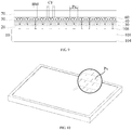
- FIG. 8 is a schematic diagram of a structure of a display device according to an example of the present disclosure.
- the display device includes a backlight source 10, and a buffer layer 20, a transistor device layer 30, a liquid crystal layer 40, a planarization layer 50, a light conversion layer 60, and a counter substrate 70 which are sequentially stackedin a direction away from the backlight source 10.
- the backlight source 10 may have a structure of any one of the backlight source 10 described above. As shown in FIG. 8 , the display device includes a plurality of sub-pixels Px (the specific number is determined according to demands). The backlight source 10 is capable of providing a collimated beam for different sub-pixels Px via different coupling gratings 106, that is, the backlight source 10 provides a separate collimated beam for each of the sub-pixels Px.
- the coupling grating 106 is provided on the upper surface of the light guide plate 101 in a manner (size, shape, positional relationship, etc.) corresponding to the manner in which the sub-pixels Px of the display device are arranged, so that the backlight source 10 provides a separate collimated beam for each sub-pixel Px of the display device via different coupling gratings 106, respectively.
- each coupling grating 106 of the backlight source 10 is aligned with a sub-pixel Px of the display device in the thickness direction, so that each collimated beam that is emitted from the coupling grating 106 and not yet incident to the buffer layer 20 is directed to the corresponding sub-pixel Px.
- each sub-pixel Px in the display region of FIG. 8 are arranged in a manner exactly same with the coupling gratings 106 in the light emitting region, and each emitting beam of the backlight source 10 is vertically incident to the corresponding sub-pixel Px. It may be understood that for a surface-type backlight source that uniformly emits light over the entire surface, each sub-pixel Px may be provided with a separate collimated beam based on the relationship between the backlight source 10 and the sub-pixel Px.
- the light emitted from the backlight source may be utilized by the sub-pixel Px in an increased proportion, which facilitates to improve the utilization of the light energy provided by the light emitting device, and further facilitates to increase the display brightness of the display device and reduce the power consumption.
- the light conversion layer 60 in the display device includes a light transmissive region CF and a light blocking region BM, and all the collimated beam provided by the backlight source 10 for any of the sub-pixels Px is directed to the light blocking region BM of the light conversion layer 60 in the sub-pixel Px.
- the collimated beam may be deflected toward the light transmissive region CF of the light conversion layer 60 as shown in FIG.
- the collimated light may be emitted passing through the light transmissive region CF, thereby enabling the sub-pixel Px to present a bright state.
- the collimated beam may not be deflected.
- the collimated beam may be emitted to and absorbed by the light blocking region BM of the light conversion layer 60, which enables the sub-pixel Px to present a dark state.
- the entire surface of the display device may present a dark state if there is no power supply, which facilitates to improve the contrast degree.
- the collimated beam may also be diverged by the optical structure between the light source 10 and the light conversion layer 60 (a beam having a relatively small divergence angle is converted to a beam having a relatively large divergence angle), so that the collimated beam that is diverged passes through the light transmissive region CF around the light blocking region BM to enable the sub-pixel Px to present a bright state, which may also be applied to enable the sub-pixel Px to switch between the bright state and the dark state.
- the light emitting device in the backlight source 10 is a blue light emitting device
- the light conversion layer 60 includes a red light transmissive region CF, a blue light transmissive region CF, and a green light transmissive region CF.
- the light conversion layer 60 in the red light transmissive region CF includes a first photoluminescent material for converting the blue light into red light
- the light conversion layer 60 in the green light transmissive region CF includes a second photoluminescent material for converting the blue light into green light.
- the sub-pixel Px in the bright state may be red, blue or green according to the type of the material in the light transmissive region, so that the display device may achieve the color display in an appropriate arrangement manner.
- the light transmissive regions CF shown in FIG. 8 may be arranged regularly from left to right in an order of: a red light transmissive region, a blue light transmissive region, a green light transmissive region, a red light transmissive region, a blue light transmissive region, and a green light transmissive region.
- the design manner of the coupling grating 106 may be adjusted with respect to the difference in the conversion efficiency of each color, so that the emitting light intensities of different colors may achieve a balance (that is, the coupling grating 106 is configured to provide emitting beams having different light intensities since the type of the corresponding sub-pixel is different).
- the light intensity of the collimated beam provided for the blue sub-pixel may be appropriately reduced, and the light intensity of the collimated beam provided for the red sub-pixel and the green sub-pixel may be appropriately increased.
- the transistor device layer 30 includes a grating layer 301, and the surface of the grating layer 301 is in contact with the liquid crystal layer 40.
- the collimated beam is directed to the light blocking region BM of the light conversion layer.
- the grating layer 301 includes a deflection grating disposed in each of the sub-pixels Px, and the deflection grating is configured to deflect the transmitted collimated beam toward the light transmissive region CF of the light conversion layer 60.
- the collimated beam is directed to the light transmissive region CF of the light conversion layer.
- the grating layer 301 includes a deflection grating disposed in each of the sub-pixels Px, and the deflection grating is configured to deflect the transmitted collimated beam toward the light blocking region BM of the light conversion layer 60.
- an expected refraction angle of the transmitted beam of the deflection grating in each sub-pixel Px may be determined according to the positional relationship between the center of the light transmissive region CF and the center of the deflection grating in the each sub-pixel Px.
- each kind of the deflection grating structure having expected optical characteristics may be obtained in advance according to, for example, any one of above mentioned design for the optical element.
- the deflection grating is manufactured on the upper surface of the transistor device layer 30 in accordance with any one of the manners that the optical element 103 is manufactured, so as to form a structure having the desired grating layer 301.
- the deflection grating may have a grating structure as shown in FIG. 2 or FIG. 3 , or may have a grating structure of a common grating that only has one valley and one ridge in each grating period, or may be not limited to this.
- the liquid crystal layer 40 may be configured to have, under the dark-state bias voltage, an edge refractive index same as the material refractive index of the grating layer 301.
- the edge refractive index refers to a refractive index for the collimated beam refracted by liquid crystal molecules that are close to the grating layer 301 for the collimated beam.
- the liquid crystal layer 40 when the liquid crystal layer 40 is located in the electric field formed by the dark-state bias voltage by selecting a liquid crystal mode in which the liquid crystal molecules are rotated in a deflection plane of the light or by using a blue phase liquid crystal, the liquid crystal molecules that are close to the grating layer 301 may be polarized in the deflection plane of the light, and the refractive index in the thickness direction of the display device for the light in the wavelength band of the collimated beam is equal to the refractive index of the material for forming the grating layer 301.
- the refractive indexes at both sides of the interface of the deflection grating are the same.
- the light may not deflect as passing through the interface of the deflection grating, which means that the deflection grating loses the function of changing the propagation direction of the collimated beam.
- the collimated beam may continue to propagate along the original propagation direction and is absorbed as arriving at the directed light blocking region BM, thereby causing the sub-pixel Px to present a dark state.
- the liquid crystal molecules in the liquid crystal layer 40 may also be in a state between the two cases.
- the display gray scale of each sub-pixel Px may be controlled by changing the applied bias voltage.
- the backlight source described above is adopted in the display device that implements the aforesaid liquid crystal display mode
- the backlight source in the display device that implements the liquid crystal display mode may not be limited to the manners described above.
- any backlight source that can provide each sub-pixel Px a collimated beam directing to the first region may be used to implement the display device in the aforesaid liquid crystal display mode.
- the extent to which the collimated beam is deflected to the second region may be controlled via different bias voltages, thereby further controlling the display gray scale of each sub-pixel Px.
- the first region and the second region are respectively one of the light blocking region BM and the light transmissive region CF of the light conversion layer 60.
- the display device is manufactured from a first substrate and a second substrate by a liquid crystal cell forming process.
- the first substrate is obtained by sequentially manufacturing the buffer layer 20 and the transistor device layer 30 on the light emitting side of the backlight source 10.
- the second substrate is obtained by sequentially manufacturing the light conversion layer 60 and the planarization layer 50 on the backlight side of the counter substrate 70.
- the buffer layer 20 may be formed of a material, such as a transparent insulating resin, silicon oxide, silicon nitride or the like, may have a refractive index of, for example, 1.2-1.4, and may mainly function to provide a flat surface to prepare for the formation of the transistor device layer 30.
- the transistor device layer 30 may include structures, such as, a gate conductive layer, a gate insulating layer, an active layer, a source/drain conductive layer, a passivation layer, a transparent conductive layer (such as, including a pattern of a pixel electrode formed of an indium tin oxide material), and a planarization layer, and may be implemented within a possible range by referring to an array substrate in any of the display devices of the prior art.
- the aforesaid grating layer 301 may be formed, for example, on the surface of the planarization layer of the transistor device layer 30, or may be disposed, for example, on the interface between two adjacent layers of the transistor device layer 30.
- the material for forming the counter substrate 70 may be, for example, transparent material, such as glass or a transparent resin, and the refractive index may be, for example, 1.5-2.0.
- the light conversion layer 60 may include, for example, a structure of a black matrix layer and a color light conversion layer, and may be implemented within a possible range by referring to a color filter substrate in any of the display devices of the prior art.
- the planarization layer 50 may be formed of a material, such as a transparent insulating resin, silicon oxide, silicon nitride or the like, and have a refractive index of, for example, 1.2-1.4.
- FIG. 9 is a schematic diagram of a structure of a display device according to another example of the present disclosure. Compared with FIG. 8 , it can be seen that settings of the grating layer 301 and the deflection grating are removed from the display device shown in FIG. 9 .
- the central position of the sub-pixel Px is set to correspond to the position of the coupling grating 106, and the liquid crystal lens formed in the liquid crystal layer 40 is adopted to control the display gray scale of each sub-pixel Px.
- the light blocking region BM in the sub-pixel Px is disposed in the center of the sub-pixel Px, and the light transmissive region CF is disposed around the light blocking region BM.
- the liquid crystal lens (such as, an equivalent lenticular lens formed by deflection of the liquid crystal molecules) is formed in the liquid crystal layer 40 to diverge the collimated beam from the coupling grating 106 , so that the collimated beam is transmitted as divergent light, and a part of the divergent light is transmitted through the light transmissive region CF, thereby achieving the bright display of the sub-pixel Px.
- the liquid crystal layer 40 When the liquid crystal layer 40 is not powered or is located in an electric field formed by a dark-state bias voltage, the liquid crystal layer 40 may not have the function to diverge the collimated beam, so that the collimated beam continues to propagate along the original propagation direction and is absorbed by the directed light blocking region BM, thereby causing the sub-pixel Px to present a dark state.
- the light emitting device in the backlight source 10 is a light emitting device of monochromatic light. Based on this, the display device may achieve monochrome display or multicolor display.
- the light conversion layer 60 is a low-haze scattering film layer in the light transmissive region CF, whereby the color of the sub-pixel Px in a bright state is the color of the light emitting device.
- the light emitting direction is not limited to the direction opposite to the propagation direction of the beam. It may be seen that the display device may achieve the monochrome display.
- the light conversion layer 60 in the light transmissive region CF includes a photoluminescent material.
- the light emitting device in the backlight source 10 is a blue light emitting device, and the light conversion layer 60 includes a red light transmissive region CF, a blue light transmissive region CF, and a green light transmissive region CF.
- the light conversion layer 60 in the red light transmissive region CF includes a first photoluminescent material for converting the blue light into red light
- the light conversion layer 60 in the green light transmissive region CF includes a second photoluminescent material for converting the blue light into green light.
- the sub-pixel Px in the bright state may be red, blue or green according to the type of the material in the light transmissive region, so that the display device may achieve the color display in an appropriate arrangement manner.
- the coupling grating 106 may be adjusted with respect to the difference in the conversion efficiency of each color, so that the emitting light intensities of different colors may achieve a balance (that is, the coupling grating 106 is configured to provide emitting beams having different light intensities since the type of the corresponding sub-pixel is different). For example, the light intensity of the collimated beam provided for the blue sub-pixel may be appropriately reduced based on examples described above, and the light intensity of the collimated beam provided for the red sub-pixel and the green sub-pixel may be appropriately increased.
- every n sub-pixels Px in any of the display devices described above constitute a pixel unit (n is a positive integer).
- each sub-pixel Px corresponds to a pixel point in the display screen.
- each pixel unit in the display device is composed of one sub-pixel Px.
- one pixel point in the display screen corresponds to three sub-pixels that are arranged in series but have different colors.
- each pixel unit in the display device is composed of a red sub-pixel, a blue sub-pixel and a green sub-pixel that are arranged in series.
- settings of the microstructure may be omitted from the pixel opening of the display device, so as to avoid the problem that the transparent region may conflict with the display region of the transparent display device, thereby facilitating to achieve a high transmittance of the transparent display device.
- settings of the polarizer or the metal polarization grid may also be omitted from the display device, thereby greatly improving the display transmittance.
- the coupling grating and the sub-pixels may be precisely aligned, thereby preventing the alignment error that occurs as forming the cell from affecting the internal optical path.
Landscapes
- Physics & Mathematics (AREA)
- Nonlinear Science (AREA)
- General Physics & Mathematics (AREA)
- Optics & Photonics (AREA)
- Mathematical Physics (AREA)
- Chemical & Material Sciences (AREA)
- Crystallography & Structural Chemistry (AREA)
- Planar Illumination Modules (AREA)
- Diffracting Gratings Or Hologram Optical Elements (AREA)
Applications Claiming Priority (2)
| Application Number | Priority Date | Filing Date | Title |
|---|---|---|---|
| CN201810004725.6A CN109991775B (zh) | 2018-01-03 | 2018-01-03 | 背光源和显示装置 |
| PCT/CN2018/123573 WO2019134562A1 (zh) | 2018-01-03 | 2018-12-25 | 背光源及其制作方法、显示装置 |
Publications (2)
| Publication Number | Publication Date |
|---|---|
| EP3736620A1 true EP3736620A1 (de) | 2020-11-11 |
| EP3736620A4 EP3736620A4 (de) | 2021-08-25 |
Family
ID=67128408
Family Applications (1)
| Application Number | Title | Priority Date | Filing Date |
|---|---|---|---|
| EP18889972.8A Withdrawn EP3736620A4 (de) | 2018-01-03 | 2018-12-25 | Hintergrundbeleuchtungsquelle, herstellungsverfahren dafür und anzeigevorrichtung |
Country Status (4)
| Country | Link |
|---|---|
| US (1) | US11860400B2 (de) |
| EP (1) | EP3736620A4 (de) |
| CN (1) | CN109991775B (de) |
| WO (1) | WO2019134562A1 (de) |
Cited By (1)
| Publication number | Priority date | Publication date | Assignee | Title |
|---|---|---|---|---|
| GB2585398B (en) * | 2018-12-06 | 2023-03-01 | Lg Display Co Ltd | Backlight unit and display device |
Families Citing this family (4)
| Publication number | Priority date | Publication date | Assignee | Title |
|---|---|---|---|---|
| CN112684629B (zh) * | 2019-10-17 | 2023-05-23 | 京东方科技集团股份有限公司 | 显示模组及其制造方法、显示装置 |
| CN113569597B (zh) * | 2020-04-29 | 2025-03-07 | 华为技术有限公司 | 物体纹路的采集装置及终端设备 |
| US20220163919A1 (en) * | 2020-11-23 | 2022-05-26 | GM Global Technology Operations LLC | Micromirror pixel design to eliminate intensity artifacts in holographic displays |
| TWI819745B (zh) * | 2022-08-11 | 2023-10-21 | 友達光電股份有限公司 | 近眼顯示裝置及其製造方法 |
Family Cites Families (19)
| Publication number | Priority date | Publication date | Assignee | Title |
|---|---|---|---|---|
| US6810176B2 (en) * | 2000-08-07 | 2004-10-26 | Rosemount Inc. | Integrated transparent substrate and diffractive optical element |
| CN101329463B (zh) * | 2007-06-18 | 2011-04-20 | 奇美电子股份有限公司 | 显示装置和液晶显示面板 |
| JP5991053B2 (ja) * | 2011-10-04 | 2016-09-14 | ソニー株式会社 | 表示装置および照明装置 |
| WO2014026923A1 (de) * | 2012-08-13 | 2014-02-20 | Bayer Materialscience Ag | Lichtführungsplatte mit auskoppelelementen |
| KR101731141B1 (ko) | 2013-12-31 | 2017-04-28 | 엘지디스플레이 주식회사 | 평판 표시장치용 박막형 백 라이트 유닛 |
| CN104460115B (zh) | 2014-12-31 | 2017-09-01 | 苏州大学 | 一种多视角像素指向型背光模组及裸眼3d显示装置 |
| KR20160084005A (ko) * | 2015-01-02 | 2016-07-13 | 삼성디스플레이 주식회사 | 액정 디스플레이 장치 |
| KR102411560B1 (ko) * | 2015-01-10 | 2022-06-21 | 레이아 인코포레이티드 | 격자 결합 광 가이드 |
| KR102364848B1 (ko) | 2015-08-20 | 2022-02-18 | 삼성전자주식회사 | 곡면형 백라이트 유닛 및 이를 포함하는 곡면형 디스플레이 장치 |
| KR102526749B1 (ko) * | 2015-09-24 | 2023-04-27 | 삼성전자주식회사 | 홀로그래픽 디스플레이용 백 라이트 유닛 |
| CN205229629U (zh) * | 2015-12-10 | 2016-05-11 | 乐视致新电子科技(天津)有限公司 | 一种背光模组、显示模组及显示设备 |
| CN206096694U (zh) * | 2016-10-24 | 2017-04-12 | 京东方科技集团股份有限公司 | 一种显示面板和装置 |
| CN106292052B (zh) | 2016-10-24 | 2019-04-09 | 京东方科技集团股份有限公司 | 一种显示面板和装置 |
| WO2018105545A1 (ja) * | 2016-12-05 | 2018-06-14 | Dic株式会社 | 液晶表示素子 |
| CN106773218B (zh) * | 2017-01-22 | 2018-07-20 | 京东方科技集团股份有限公司 | 显示装置 |
| CN107167925A (zh) * | 2017-06-08 | 2017-09-15 | 东南大学 | 一种全息光栅背光结构的场序三维显示器 |
| CN107479128A (zh) | 2017-09-21 | 2017-12-15 | 京东方科技集团股份有限公司 | 背光模组和显示装置 |
| CN107450211B (zh) * | 2017-09-29 | 2021-04-16 | 京东方科技集团股份有限公司 | 灰阶控制结构及其方法、液晶显示面板、显示装置 |
| CN107450234A (zh) * | 2017-10-10 | 2017-12-08 | 京东方科技集团股份有限公司 | 显示基板、显示面板及显示装置 |
-
2018
- 2018-01-03 CN CN201810004725.6A patent/CN109991775B/zh not_active Expired - Fee Related
- 2018-12-25 EP EP18889972.8A patent/EP3736620A4/de not_active Withdrawn
- 2018-12-25 WO PCT/CN2018/123573 patent/WO2019134562A1/zh not_active Ceased
- 2018-12-25 US US16/474,574 patent/US11860400B2/en active Active
Cited By (1)
| Publication number | Priority date | Publication date | Assignee | Title |
|---|---|---|---|---|
| GB2585398B (en) * | 2018-12-06 | 2023-03-01 | Lg Display Co Ltd | Backlight unit and display device |
Also Published As
| Publication number | Publication date |
|---|---|
| CN109991775A (zh) | 2019-07-09 |
| CN109991775B (zh) | 2020-06-30 |
| EP3736620A4 (de) | 2021-08-25 |
| WO2019134562A1 (zh) | 2019-07-11 |
| US20220011497A1 (en) | 2022-01-13 |
| US11860400B2 (en) | 2024-01-02 |
Similar Documents
| Publication | Publication Date | Title |
|---|---|---|
| US11860400B2 (en) | Backlight component, method for manufacturing backlight component, and display device | |
| US10976595B2 (en) | Optical substrate and display device | |
| US10768481B2 (en) | Direct type backlight and method of manufacturing the same, and display device | |
| US11487057B2 (en) | Optical substrate and display device | |
| CN107817629B (zh) | 一种液晶显示装置 | |
| CN109239965B (zh) | 一种显示器件及其控制方法 | |
| US11537004B2 (en) | Transparent display substrate and transparent display device | |
| CN109765721B (zh) | 一种前置光源模组、显示装置、显示方法及制作方法 | |
| CN110389469B (zh) | 显示装置及其显示方法 | |
| CN109799568B (zh) | 一种背光模组及显示装置 | |
| US11150398B2 (en) | Edge-lit type backlight module and display device | |
| CN108646338A (zh) | 一种背光模组及显示装置 | |
| US11391877B2 (en) | Backlight source and manufacturing method thereof, and display device | |
| KR20150079800A (ko) | 조명 디바이스 | |
| WO2019029349A1 (zh) | 背光组件及其制备方法和显示装置 | |
| US20190285935A1 (en) | Display panel and method for fabricating the same, display device and display method | |
| CN108646493A (zh) | 一种显示装置 | |
| CN107315280A (zh) | 背光模组及其制作方法、显示装置 | |
| CN104704407A (zh) | 带有退耦元件的光引导板 | |
| CN107247365A (zh) | 背光模组及显示装置 | |
| CN105929591B (zh) | 量子点显示基板及其制造方法和量子点显示装置 | |
| US11327360B2 (en) | Display panel, display apparatus, driving method of the display panel, and storage medium | |
| KR20080062766A (ko) | 반사 투과형 디스플레이 패널 및 이를 채용한 디스플레이장치 | |
| CN108663858A (zh) | 背光模组、显示装置及其驱动方法 | |
| US20200379163A1 (en) | Display panel and display device |
Legal Events
| Date | Code | Title | Description |
|---|---|---|---|
| STAA | Information on the status of an ep patent application or granted ep patent |
Free format text: STATUS: UNKNOWN |
|
| STAA | Information on the status of an ep patent application or granted ep patent |
Free format text: STATUS: THE INTERNATIONAL PUBLICATION HAS BEEN MADE |
|
| PUAI | Public reference made under article 153(3) epc to a published international application that has entered the european phase |
Free format text: ORIGINAL CODE: 0009012 |
|
| STAA | Information on the status of an ep patent application or granted ep patent |
Free format text: STATUS: REQUEST FOR EXAMINATION WAS MADE |
|
| 17P | Request for examination filed |
Effective date: 20190628 |
|
| AK | Designated contracting states |
Kind code of ref document: A1 Designated state(s): AL AT BE BG CH CY CZ DE DK EE ES FI FR GB GR HR HU IE IS IT LI LT LU LV MC MK MT NL NO PL PT RO RS SE SI SK SM TR |
|
| AX | Request for extension of the european patent |
Extension state: BA ME |
|
| DAV | Request for validation of the european patent (deleted) | ||
| DAX | Request for extension of the european patent (deleted) | ||
| A4 | Supplementary search report drawn up and despatched |
Effective date: 20210727 |
|
| RIC1 | Information provided on ipc code assigned before grant |
Ipc: G02F 1/1335 20060101AFI20210721BHEP Ipc: G02F 1/1343 20060101ALI20210721BHEP Ipc: G02B 6/34 20060101ALI20210721BHEP Ipc: G02F 1/13357 20060101ALI20210721BHEP Ipc: G02B 6/00 20060101ALI20210721BHEP |
|
| STAA | Information on the status of an ep patent application or granted ep patent |
Free format text: STATUS: THE APPLICATION HAS BEEN WITHDRAWN |
|
| 18W | Application withdrawn |
Effective date: 20220928 |