EP3731288B1 - Use of an electric field for detaching a piezoelectric layer from a donor substrate - Google Patents
Use of an electric field for detaching a piezoelectric layer from a donor substrate Download PDFInfo
- Publication number
- EP3731288B1 EP3731288B1 EP20180045.5A EP20180045A EP3731288B1 EP 3731288 B1 EP3731288 B1 EP 3731288B1 EP 20180045 A EP20180045 A EP 20180045A EP 3731288 B1 EP3731288 B1 EP 3731288B1
- Authority
- EP
- European Patent Office
- Prior art keywords
- piezoelectric
- donor substrate
- substrate
- electric field
- detaching
- Prior art date
- Legal status (The legal status is an assumption and is not a legal conclusion. Google has not performed a legal analysis and makes no representation as to the accuracy of the status listed.)
- Active
Links
- 239000000758 substrate Substances 0.000 title claims description 101
- 230000005684 electric field Effects 0.000 title claims description 30
- 150000001875 compounds Chemical class 0.000 claims description 10
- 238000010438 heat treatment Methods 0.000 claims description 10
- 239000000919 ceramic Substances 0.000 claims description 3
- 238000000034 method Methods 0.000 description 22
- UNILWMWFPHPYOR-KXEYIPSPSA-M 1-[6-[2-[3-[3-[3-[2-[2-[3-[[2-[2-[[(2r)-1-[[2-[[(2r)-1-[3-[2-[2-[3-[[2-(2-amino-2-oxoethoxy)acetyl]amino]propoxy]ethoxy]ethoxy]propylamino]-3-hydroxy-1-oxopropan-2-yl]amino]-2-oxoethyl]amino]-3-[(2r)-2,3-di(hexadecanoyloxy)propyl]sulfanyl-1-oxopropan-2-yl Chemical compound O=C1C(SCCC(=O)NCCCOCCOCCOCCCNC(=O)COCC(=O)N[C@@H](CSC[C@@H](COC(=O)CCCCCCCCCCCCCCC)OC(=O)CCCCCCCCCCCCCCC)C(=O)NCC(=O)N[C@H](CO)C(=O)NCCCOCCOCCOCCCNC(=O)COCC(N)=O)CC(=O)N1CCNC(=O)CCCCCN\1C2=CC=C(S([O-])(=O)=O)C=C2CC/1=C/C=C/C=C/C1=[N+](CC)C2=CC=C(S([O-])(=O)=O)C=C2C1 UNILWMWFPHPYOR-KXEYIPSPSA-M 0.000 description 9
- 238000007669 thermal treatment Methods 0.000 description 9
- 230000010287 polarization Effects 0.000 description 6
- 229910012463 LiTaO3 Inorganic materials 0.000 description 5
- 230000000694 effects Effects 0.000 description 5
- 150000002500 ions Chemical class 0.000 description 5
- 230000003313 weakening effect Effects 0.000 description 5
- 229910003327 LiNbO3 Inorganic materials 0.000 description 4
- 230000007547 defect Effects 0.000 description 3
- 239000000463 material Substances 0.000 description 3
- 229910052594 sapphire Inorganic materials 0.000 description 3
- 239000010980 sapphire Substances 0.000 description 3
- 239000002131 composite material Substances 0.000 description 2
- 230000002950 deficient Effects 0.000 description 2
- 238000005468 ion implantation Methods 0.000 description 2
- 238000004519 manufacturing process Methods 0.000 description 2
- 239000002184 metal Substances 0.000 description 2
- 239000004065 semiconductor Substances 0.000 description 2
- 238000000926 separation method Methods 0.000 description 2
- 229910052710 silicon Inorganic materials 0.000 description 2
- 239000010703 silicon Substances 0.000 description 2
- 230000000295 complement effect Effects 0.000 description 1
- 239000012212 insulator Substances 0.000 description 1
- 239000000203 mixture Substances 0.000 description 1
Images

Classifications
-
- H—ELECTRICITY
- H10—SEMICONDUCTOR DEVICES; ELECTRIC SOLID-STATE DEVICES NOT OTHERWISE PROVIDED FOR
- H10N—ELECTRIC SOLID-STATE DEVICES NOT OTHERWISE PROVIDED FOR
- H10N30/00—Piezoelectric or electrostrictive devices
- H10N30/01—Manufacture or treatment
- H10N30/08—Shaping or machining of piezoelectric or electrostrictive bodies
- H10N30/085—Shaping or machining of piezoelectric or electrostrictive bodies by machining
-
- H—ELECTRICITY
- H10—SEMICONDUCTOR DEVICES; ELECTRIC SOLID-STATE DEVICES NOT OTHERWISE PROVIDED FOR
- H10N—ELECTRIC SOLID-STATE DEVICES NOT OTHERWISE PROVIDED FOR
- H10N30/00—Piezoelectric or electrostrictive devices
- H10N30/01—Manufacture or treatment
- H10N30/07—Forming of piezoelectric or electrostrictive parts or bodies on an electrical element or another base
- H10N30/072—Forming of piezoelectric or electrostrictive parts or bodies on an electrical element or another base by laminating or bonding of piezoelectric or electrostrictive bodies
-
- H—ELECTRICITY
- H10—SEMICONDUCTOR DEVICES; ELECTRIC SOLID-STATE DEVICES NOT OTHERWISE PROVIDED FOR
- H10N—ELECTRIC SOLID-STATE DEVICES NOT OTHERWISE PROVIDED FOR
- H10N30/00—Piezoelectric or electrostrictive devices
- H10N30/01—Manufacture or treatment
- H10N30/06—Forming electrodes or interconnections, e.g. leads or terminals
-
- H—ELECTRICITY
- H10—SEMICONDUCTOR DEVICES; ELECTRIC SOLID-STATE DEVICES NOT OTHERWISE PROVIDED FOR
- H10N—ELECTRIC SOLID-STATE DEVICES NOT OTHERWISE PROVIDED FOR
- H10N30/00—Piezoelectric or electrostrictive devices
- H10N30/1051—Piezoelectric or electrostrictive devices based on piezoelectric or electrostrictive films or coatings
-
- H—ELECTRICITY
- H10—SEMICONDUCTOR DEVICES; ELECTRIC SOLID-STATE DEVICES NOT OTHERWISE PROVIDED FOR
- H10N—ELECTRIC SOLID-STATE DEVICES NOT OTHERWISE PROVIDED FOR
- H10N30/00—Piezoelectric or electrostrictive devices
- H10N30/80—Constructional details
- H10N30/85—Piezoelectric or electrostrictive active materials
- H10N30/853—Ceramic compositions
- H10N30/8536—Alkaline earth metal based oxides, e.g. barium titanates
-
- H—ELECTRICITY
- H10—SEMICONDUCTOR DEVICES; ELECTRIC SOLID-STATE DEVICES NOT OTHERWISE PROVIDED FOR
- H10N—ELECTRIC SOLID-STATE DEVICES NOT OTHERWISE PROVIDED FOR
- H10N30/00—Piezoelectric or electrostrictive devices
- H10N30/80—Constructional details
- H10N30/85—Piezoelectric or electrostrictive active materials
- H10N30/853—Ceramic compositions
- H10N30/8542—Alkali metal based oxides, e.g. lithium, sodium or potassium niobates
-
- H—ELECTRICITY
- H10—SEMICONDUCTOR DEVICES; ELECTRIC SOLID-STATE DEVICES NOT OTHERWISE PROVIDED FOR
- H10N—ELECTRIC SOLID-STATE DEVICES NOT OTHERWISE PROVIDED FOR
- H10N30/00—Piezoelectric or electrostrictive devices
- H10N30/80—Constructional details
- H10N30/85—Piezoelectric or electrostrictive active materials
- H10N30/853—Ceramic compositions
- H10N30/8548—Lead based oxides
- H10N30/8554—Lead zirconium titanate based
-
- H—ELECTRICITY
- H01—ELECTRIC ELEMENTS
- H01L—SEMICONDUCTOR DEVICES NOT COVERED BY CLASS H10
- H01L2221/00—Processes or apparatus adapted for the manufacture or treatment of semiconductor or solid state devices or of parts thereof covered by H01L21/00
- H01L2221/67—Apparatus for handling semiconductor or electric solid state devices during manufacture or treatment thereof; Apparatus for handling wafers during manufacture or treatment of semiconductor or electric solid state devices or components; Apparatus not specifically provided for elsewhere
- H01L2221/683—Apparatus for handling semiconductor or electric solid state devices during manufacture or treatment thereof; Apparatus for handling wafers during manufacture or treatment of semiconductor or electric solid state devices or components; Apparatus not specifically provided for elsewhere for supporting or gripping
- H01L2221/68304—Apparatus for handling semiconductor or electric solid state devices during manufacture or treatment thereof; Apparatus for handling wafers during manufacture or treatment of semiconductor or electric solid state devices or components; Apparatus not specifically provided for elsewhere for supporting or gripping using temporarily an auxiliary support
- H01L2221/68363—Apparatus for handling semiconductor or electric solid state devices during manufacture or treatment thereof; Apparatus for handling wafers during manufacture or treatment of semiconductor or electric solid state devices or components; Apparatus not specifically provided for elsewhere for supporting or gripping using temporarily an auxiliary support used in a transfer process involving transfer directly from an origin substrate to a target substrate without use of an intermediate handle substrate
-
- H—ELECTRICITY
- H10—SEMICONDUCTOR DEVICES; ELECTRIC SOLID-STATE DEVICES NOT OTHERWISE PROVIDED FOR
- H10N—ELECTRIC SOLID-STATE DEVICES NOT OTHERWISE PROVIDED FOR
- H10N30/00—Piezoelectric or electrostrictive devices
- H10N30/01—Manufacture or treatment
- H10N30/04—Treatments to modify a piezoelectric or electrostrictive property, e.g. polarisation characteristics, vibration characteristics or mode tuning
-
- Y—GENERAL TAGGING OF NEW TECHNOLOGICAL DEVELOPMENTS; GENERAL TAGGING OF CROSS-SECTIONAL TECHNOLOGIES SPANNING OVER SEVERAL SECTIONS OF THE IPC; TECHNICAL SUBJECTS COVERED BY FORMER USPC CROSS-REFERENCE ART COLLECTIONS [XRACs] AND DIGESTS
- Y10—TECHNICAL SUBJECTS COVERED BY FORMER USPC
- Y10T—TECHNICAL SUBJECTS COVERED BY FORMER US CLASSIFICATION
- Y10T29/00—Metal working
- Y10T29/42—Piezoelectric device making
Definitions
- a method for transferring a piezoelectric layer onto a support substrate, that is not part of the invention, is described.
- the invention relates to a detaching chamber for carrying out at least a part of the method.
- patent document US2010088868 discloses a supporting substrate bonded to the surface of the piezoelectric substrate to form a bonded substrate body, the bonded substrate body is separated at the defective layer formed in the piezoelectric substrate so that a separation layer between the surface of the piezoelectric substrate and the defective layer is separated from the piezoelectric substrate and bonded to the supporting substrate to form a composite piezoelectric substrate, and the surface of the separation layer of the composite piezoelectric substrate is smoothed.
- the process could make use of a piezoelectric donor substrate with a predetermined splitting area inside the donor substrate.
- the predetermined splitting area can be obtained by implanting ions into the donor substrate.
- the donor substrate is subsequently attached to the support substrate and undergoes a thermal treatment to strengthen the bond between the donor and the support substrate and to detach the remainder of the donor substrate at the predetermined splitting area to thereby transfer a layer of the piezoelectric donor substrate onto the support substrate.
- the defaults created in the predetermined splitting area by the implanted ions grow leading to local strain which at a given thermal budget leads to the detachment and thereby to the layer transfer onto the support substrate.
- This object is achieved with the method of transferring a piezoelectric layer onto a support substrate and which comprises the steps of: a) providing a predetermined splitting area in a piezoelectric donor substrate, b) attaching the piezoelectric donor substrate to a support substrate to form a compound, and c) detaching the piezoelectric layer from the piezoelectric donor substrate comprising applying an electric field.
- an electric field use is made of the piezoelectric properties of the donor substrate to weaken the predetermined splitting area, as the electric field will introduce a deformation within the piezoelectric donor substrate and further weaken the area of the defaults in the predetermined splitting area due to building up complementary strain. As a consequence, the thermal budget necessary for the complete detachment of the piezoelectric layer to be detached can be lower.
- the piezoelectric donor substrate may be made of a single piezoelectric material, a so-called bulk piezoelectric substrate.
- the piezoelectric donor substrate may be made of a layer of piezoelectric material provided on a handle substrate.
- a handle substrate may be chosen with a similar CTE with respect to the support substrate. A difference in CTE between handle and support substrate that is lower than 10%, with respect to the larger of the two CTE, allows a higher thermal budget for the thermal treatments assisting the above described method compared to higher differences in the CTE and/or compared to the use of bulk piezoelectric substrates with a higher CTE difference with respect to the support substrate.
- the method can further comprise an ion implantation step to form the predetermined splitting area and a thermal treatment step of the ion implanted piezoelectric donor substrate wherein the thermal treatment step can be carried out in a temperature range of 0°C to 200°C for a duration between 1h to 24h.
- the thermal treatment step thereby may allow the defects in the predetermined splitting area to grow.
- step b) can comprise a heat treatment with a temperature of at most 100°C or at most 50°C or in a variant can be carried out at room temperature in between 15°C to 25°C.
- the bonding interface needs to be stabilized prior to the detachment step to prevent unwanted bonding defects at the moment of detachment.
- the enhancement of the bonding is obtained by heating the compound prior to detachment. As already mentioned above such a heat treatment leads to problems related to the difference in thermal expansion coefficient in case of a piezoelectric donor substrate.
- the bonding energy between the donor substrate and the support substrate can be lower compared to the bonding energy necessary for a thermally induced detachment only. This due to the fact that the impact of the mechanical distortion due to the presence of the electric field is very much limited to the piezoelectric donor substrate and has a lower impact on the interface with the support substrate.
- step b) can be carried out at a pressure below 10 -2 mbar.
- step c) can be carried out at a temperature of less than 100°C, more in particular less than 50°C, even more in particular at room temperature in between 15°C to 25°C.
- the detachment can be obtained at lower temperature compared to a detachment process that is not assisted by an electric field.
- the electric field can be applied using a chuck comprising at least one electrode.
- a chuck comprising at least one electrode.
- the chuck may comprise holding means which are independent of such electrodes and being implemented by for instance vacuum or electrostatic properties.
- the surface of the piezoelectric donor substrate of the compound can be placed onto the chuck.
- the process can be carried out independently of the electric properties of the support substrate.
- the chuck can comprise interdigitated electrodes separated by an electric isolator, in particular a ceramic.
- an electric isolator in particular a ceramic.
- this geometry it is possible to create a suitable electric field using only one electrode. This keeps the design of the processing chamber simple.
- the voltage applied to the chuck can be of up to 10kV, in particular in a range between 1kV and 5kV. In this voltage range a sufficiently strong electric field is formed in order to deform the piezoelectric donor substrate such that detachment can occur at a lower thermal budget.
- the donor substrate - support substrate compound can be sandwiched between the chuck and a second electrode, in particular being comprised in a second chuck.
- the voltage applied to the first and second electrodes can be lower than in case of only one electrode.
- the voltage applied to the electrostatic chuck can be of up to 5kV, in particular in a range between 200V and 1kV.
- the electric field lines can be essentially parallel to the polarization direction of the piezoelectric donor substrate. By aligning the electric field to the polarization direction of the piezoelectric donor substrate the amplitude of the resulting distortion can be enhanced and the detachment step facilitated.
- the piezoelectric donor substrate can be one of LiTaO 3 (LTO), AIN, ZnO,
- the support substrate can be a semiconductor substrate, in particular a Si wafer, or an isolator, in particular a sapphire wafer, or a metal, in particular a Mo wafer.
- the object of the invention is achieved with a detaching chamber for carrying out step c) as described above and which comprises one or two chucks for applying an electric field to a piezoelectric layer.
- the detaching chamber could, according to a variant, also be used for carrying out step b).
- the use of the chuck allows the creation of an electrical field which leads to a deformation in the piezoelectric substrate thereby weakening the predetermined splitting area.
- the thermal budget necessary to perform the detachment of the piezoelectric layer from the remainder of the donor substrate can be lower compared to a process using only the thermal energy for the detachment step.
- the negative impact of a large difference in the thermal expansion coefficient between the donor substrate and the support substrate can be reduced.
- the object of the invention is also achieved with a chuck that comprises holding means for holding the compound, in particular vacuum and/or electrostatic holding means and electrodes for applying an electric field for weakening a predetermined splitting area inside the compound.
- the electrostatic holding means and the electrodes for applying the electrical filed can be independent from each other. In this way, the holding action and the weakening action as described above with respect to the method can be optimized with respect to each other.
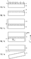
- Figures 1a to 1e illustrate an embodiment of the method, not part of the invention, of transferring a piezoelectric layer onto a support substrate.
- a predetermined splitting area 1 is created in a piezoelectric donor substrate 3 by implanting ions 5.
- the piezoelectric donor substrate 3 can e.g. be LiTaO 3 (LTO), AIN, ZnO, Pb[Zr x Ti 1-x ]O 3 (0 ⁇ x ⁇ 1) (PZT) and LiNbO 3 (LNO).
- the piezoelectric donor substrate is a bulk piezoelectric substrate made of LTO.
- the donor substrate could comprise a handle substrate with a piezoelectric layer on top of it.
- the predetermined splitting area 1 inside the piezoelectric donor substrate 3 5*10 16 to 2*10 17 H + or He + or a mix of H + /He + ions/cm 2 are implanted with an energy of about 10keV to 1 MeV as a function of the desired depth d of the predetermined splitting area 1. Under the implanting conditions mentioned above, the depth d is of the order of 60nm to 6 ⁇ m.
- the next step, illustrated in Figure 1b is a first thermal treatment step to let the defects 7 forming the predetermined splitting area 1 created by the ion implantation, grow.
- the roughness of the surface 9 is below 5nm RMS.
- this first thermal treatment step is carried out at temperatures between 0°C and 200°C for a duration of about 1 to 24hrs.
- Step b) is illustrated in Figure 1c . It consists in attaching, in particular by bonding, the piezoelectric donor substrate 3 to a support substrate 11 to thereby form a compound 13.
- the support substrate 11 can be semiconductor substrate, like a Si wafer, or an isolator, like sapphire, or a metal, like Mo.
- the bonding step is carried out at ambient pressure or under vacuum, typically a primary vacuum of below 10 -2 mbar, in particular of the order of 10 -3 to 10 -4 mbar.
- the bonding is carried out at a temperature of up to 100°C.
- FIG. 1d illustrates the next step in the manufacturing process.
- This step corresponds to step c).
- An electric field is applied to the compound 13, with the electric field lines 15 essentially perpendicular to the predetermined splitting area 1.
- the electric field lines 15 are essentially parallel to the polarization axis 17 (or poling axis) of the piezoelectric donor substrate 3 to optimize the piezoelectric effect. Due to the piezoelectric properties, the presence of the electric field 15 will lead to a mechanical deformation in the direction z inside the piezoelectric support substrate 3. This deformation further weakens the predetermined splitting area 1.
- voltages of up to 10kV are applied (see description further down with respect to figures 2 and 3 ).
- a complete detachment of the remainder 19 of the piezoelectric donor substrate from the modified compound 13' comprising the support substrate 11 and a transferred piezoelectric layer 21 can occur at the predetermined splitting area as illustrated in Figure 1e .
- the detachment as shown in Figure 1e can also be obtained by heating the compound 13 during or after the application of the electric field 15.
- temperatures of up to 100°C are used for the final detachment. The choice of the temperature depends on the conditions of first heat treatment step and the strength of the electric field 15.
- the remainder 19 of the piezoelectric donor substrate can then be reused as a donor substrate 3 to restart the process as described with respect to Figures 1a to 1e .
- Figure 2 schematically illustrates a setup according to a second embodiment of the invention.
- Figure 2 shows a detaching chamber 31 used to carry out at least step c) of the method according to the invention as illustrated in Figure 1d .
- the detaching chamber comprises a chuck 33 comprising positive electrodes 35 and negative electrodes 37 to be able to apply an electric field 39 to the compound 13 comprising the piezoelectric donor substrate 3 and the support substrate 11 as described in detail with respect to the first embodiment, not part of the invention.
- the description of the features of the first embodiment, not part of the invention, will not be repeated again, but is incorporated herewith by reference.
- the chuck may comprise further means for holding the compound 13, e.g. vacuum of electrostatic means. In this embodiment, those are independent of the electrodes 35 and 37.
- the compound 13 is positioned on the chuck 33 such that the piezoelectric donor substrate 3 of the compound 13 is placed onto the chuck 33.
- the positive and negative electrodes 35, 37 are arranged such that the electric field 39 is essentially perpendicular to the surface of the chuck 33 at least within the thickness d' of the piezoelectric donor substrate 3. With the polarization axis 17 of the piezoelectric donor substrate also being perpendicular to the chuck 33, the piezoelectric effect can be optimized thereby creating mechanical strain in the predetermined splitting area 1 further leading to weakening.
- the support substrate that is positioned on the chuck 33, especially in case the electric field is strong enough.
- the positive electrodes 35 and negative electrodes 37 are interdigitated with an electric isolator (not shown), e.g. a thin ceramic layer, positioned in between.
- the control unit of the splitting chamber 31 is configured such that electric tensions of up to 10kV can be applied to the electrodes, preferably, 1kV to 5kV. In this embodiment only one electrostatic chuck is necessary which simplifies the design of the detaching chamber 31.
- Figure 3 schematically illustrates a setup according to a third embodiment of the invention.
- Figure 3 shows a second embodiment of a detaching chamber 51 used to carry out at least step c) of the method not according to the invention as illustrated in Figure 1d .
- the description of the features of the first and second embodiment will not be repeated again, but is incorporated herewith by reference.
- two chucks 53 and 55 are used.
- the lower chuck 53 comprises a positive electrode 57; the upper chuck 55 comprises a negative electrode 59.
- the polarization can be exchanged.
- the compound 13 is sandwiched between the two chucks 53, 55.
- the electric field lines 61 are parallel to the polarization direction 17 of the piezoelectric donor substrate to optimize the piezoelectric effect leading to optimized weakening in the predetermined splitting area 1.
- the detaching chamber 31, 51 of the second and third embodiment may, according to further variants, be used for step b) of the method not according to the invention, thus to realize the attachment step as illustrated in Figure 1c . Furthermore it may, according to additional variants, also comprise heating means and/or a vacuum pump to be able to carry out the heat treatments and/or carry out the process steps under vacuum.
Description
- A method for transferring a piezoelectric layer onto a support substrate, that is not part of the invention, is described. The invention, relates to a detaching chamber for carrying out at least a part of the method.
- There is raising interest in compound structures comprising a support substrate, like Silicon or Sapphire, with a thin piezoelectric layer attached thereto. It has been proposed to use a SmartCut™ type process, known from Silicon on Insulator substrates, to obtain such a compound structure. An example of the prior art may be found in patent document
US2010088868 which discloses a supporting substrate bonded to the surface of the piezoelectric substrate to form a bonded substrate body, the bonded substrate body is separated at the defective layer formed in the piezoelectric substrate so that a separation layer between the surface of the piezoelectric substrate and the defective layer is separated from the piezoelectric substrate and bonded to the supporting substrate to form a composite piezoelectric substrate, and the surface of the separation layer of the composite piezoelectric substrate is smoothed. - The process could make use of a piezoelectric donor substrate with a predetermined splitting area inside the donor substrate. The predetermined splitting area can be obtained by implanting ions into the donor substrate. The donor substrate is subsequently attached to the support substrate and undergoes a thermal treatment to strengthen the bond between the donor and the support substrate and to detach the remainder of the donor substrate at the predetermined splitting area to thereby transfer a layer of the piezoelectric donor substrate onto the support substrate.
- Under the effect of the higher temperature during the thermal treatment, the defaults created in the predetermined splitting area by the implanted ions grow leading to local strain which at a given thermal budget leads to the detachment and thereby to the layer transfer onto the support substrate.
- In case of a piezoelectric donor substrate, it is, however, difficult to transfer the layer without breakage. This is due to the large difference in thermal expansion coefficients between the piezoelectric donor substrate and the support substrate (CTE mismatch). Thus, strain develops during the heat treatment at the interface of the donor and support substrate which suddenly relaxes at the moment of detachment and leads to the breakage of the transferred layer.
- There is provided, an alternative layer transferring method which is particularly important to reduce breakage of the transferred piezoelectric layer due to CTE mismatch.
- This object is achieved with the method of transferring a piezoelectric layer onto a support substrate and which comprises the steps of: a) providing a predetermined splitting area in a piezoelectric donor substrate, b) attaching the piezoelectric donor substrate to a support substrate to form a compound, and c) detaching the piezoelectric layer from the piezoelectric donor substrate comprising applying an electric field. By applying an electric field use is made of the piezoelectric properties of the donor substrate to weaken the predetermined splitting area, as the electric field will introduce a deformation within the piezoelectric donor substrate and further weaken the area of the defaults in the predetermined splitting area due to building up complementary strain. As a consequence, the thermal budget necessary for the complete detachment of the piezoelectric layer to be detached can be lower.
- According to certain embodiments, the piezoelectric donor substrate may be made of a single piezoelectric material, a so-called bulk piezoelectric substrate. According to other embodiments, the piezoelectric donor substrate may be made of a layer of piezoelectric material provided on a handle substrate. In the second case, a handle substrate may be chosen with a similar CTE with respect to the support substrate. A difference in CTE between handle and support substrate that is lower than 10%, with respect to the larger of the two CTE, allows a higher thermal budget for the thermal treatments assisting the above described method compared to higher differences in the CTE and/or compared to the use of bulk piezoelectric substrates with a higher CTE difference with respect to the support substrate.
- According to an embodiment, the method can further comprise an ion implantation step to form the predetermined splitting area and a thermal treatment step of the ion implanted piezoelectric donor substrate wherein the thermal treatment step can be carried out in a temperature range of 0°C to 200°C for a duration between 1h to 24h. The thermal treatment step thereby may allow the defects in the predetermined splitting area to grow.
- According to a preferred variant, step b) can comprise a heat treatment with a temperature of at most 100°C or at most 50°C or in a variant can be carried out at room temperature in between 15°C to 25°C. In a manufacturing process in which the detachment is achieved by a thermal treatment only, the bonding interface needs to be stabilized prior to the detachment step to prevent unwanted bonding defects at the moment of detachment. In the prior art, the enhancement of the bonding is obtained by heating the compound prior to detachment. As already mentioned above such a heat treatment leads to problems related to the difference in thermal expansion coefficient in case of a piezoelectric donor substrate. By using an electric field during the detachment, the bonding energy between the donor substrate and the support substrate can be lower compared to the bonding energy necessary for a thermally induced detachment only. This due to the fact that the impact of the mechanical distortion due to the presence of the electric field is very much limited to the piezoelectric donor substrate and has a lower impact on the interface with the support substrate.
- According to a preferred variant, step b) can be carried out at a pressure below 10-2 mbar.
- Preferably, step c) can be carried out at a temperature of less than 100°C, more in particular less than 50°C, even more in particular at room temperature in between 15°C to 25°C. Thus, the detachment can be obtained at lower temperature compared to a detachment process that is not assisted by an electric field.
- According to a preferred embodiment, the electric field can be applied using a chuck comprising at least one electrode. By using such chuck, the electric field can be made available in a simple manner. The chuck may comprise holding means which are independent of such electrodes and being implemented by for instance vacuum or electrostatic properties.
- Advantageously, the surface of the piezoelectric donor substrate of the compound can be placed onto the chuck. In this arrangement, the process can be carried out independently of the electric properties of the support substrate.
- According to a variant, the chuck can comprise interdigitated electrodes separated by an electric isolator, in particular a ceramic. In this geometry it is possible to create a suitable electric field using only one electrode. This keeps the design of the processing chamber simple.
- According to an embodiment, the voltage applied to the chuck can be of up to 10kV, in particular in a range between 1kV and 5kV. In this voltage range a sufficiently strong electric field is formed in order to deform the piezoelectric donor substrate such that detachment can occur at a lower thermal budget.
- According to a variant, the donor substrate - support substrate compound can be sandwiched between the chuck and a second electrode, in particular being comprised in a second chuck. In a design using an electrode on both sides of the compound, the voltage applied to the first and second electrodes can be lower than in case of only one electrode. Preferably, in this variant of the invention, the voltage applied to the electrostatic chuck can be of up to 5kV, in particular in a range between 200V and 1kV.
- According to an embodiment, the electric field lines can be essentially parallel to the polarization direction of the piezoelectric donor substrate. By aligning the electric field to the polarization direction of the piezoelectric donor substrate the amplitude of the resulting distortion can be enhanced and the detachment step facilitated.
- Preferably, the piezoelectric donor substrate can be one of LiTaO3 (LTO), AIN, ZnO,
- Pb[ZrxTi1-x]O3 (0≤x≤1) (PZT) and LiNbO3 (LNO). Preferably, the support substrate can be a semiconductor substrate, in particular a Si wafer, or an isolator, in particular a sapphire wafer, or a metal, in particular a Mo wafer.
- The object of the invention is achieved with a detaching chamber for carrying out step c) as described above and which comprises one or two chucks for applying an electric field to a piezoelectric layer. The detaching chamber could, according to a variant, also be used for carrying out step b). The use of the chuck allows the creation of an electrical field which leads to a deformation in the piezoelectric substrate thereby weakening the predetermined splitting area. As a consequence the thermal budget necessary to perform the detachment of the piezoelectric layer from the remainder of the donor substrate can be lower compared to a process using only the thermal energy for the detachment step. Thus, the negative impact of a large difference in the thermal expansion coefficient between the donor substrate and the support substrate can be reduced.
- The object of the invention is also achieved with a chuck that comprises holding means for holding the compound, in particular vacuum and/or electrostatic holding means and electrodes for applying an electric field for weakening a predetermined splitting area inside the compound. According to a variant, the electrostatic holding means and the electrodes for applying the electrical filed can be independent from each other. In this way, the holding action and the weakening action as described above with respect to the method can be optimized with respect to each other.
- The present invention will be explained more in detail hereafter using advantageous exemplary embodiments in conjunction with the accompanying figures, wherein:
- Figures 1a to 1e
- schematically illustrate the method of transferring a piezoelectric layer onto a support substrate, which is not part of the invention
- Figure 2
- schematically illustrates a setup according to a second embodiment of the invention,
- Figure 3
- schematically illustrates a setup according to a third embodiment of the invention.
-
Figures 1a to 1e illustrate an embodiment of the method, not part of the invention, of transferring a piezoelectric layer onto a support substrate. - In the process step illustrated in
Figure 1a , corresponding to step a) of the method not according to the invention, apredetermined splitting area 1 is created in apiezoelectric donor substrate 3 by implanting ions 5. - The
piezoelectric donor substrate 3 can e.g. be LiTaO3 (LTO), AIN, ZnO, Pb[ZrxTi1-x]O3 (0≤x≤1) (PZT) and LiNbO3 (LNO). In the following, as an example not according to the invention, the piezoelectric donor substrate is a bulk piezoelectric substrate made of LTO. According to a variant, the donor substrate could comprise a handle substrate with a piezoelectric layer on top of it. - To obtain the
predetermined splitting area 1 inside thepiezoelectric donor substrate 3 5*1016 to 2*1017 H+ or He+ or a mix of H+/He+ ions/cm2 are implanted with an energy of about 10keV to 1 MeV as a function of the desired depth d of thepredetermined splitting area 1. Under the implanting conditions mentioned above, the depth d is of the order of 60nm to 6µm. - The next step, illustrated in
Figure 1b , is a first thermal treatment step to let thedefects 7 forming thepredetermined splitting area 1 created by the ion implantation, grow. The roughness of thesurface 9 is below 5nm RMS. According to the invention, this first thermal treatment step is carried out at temperatures between 0°C and 200°C for a duration of about 1 to 24hrs. Step b) is illustrated inFigure 1c . It consists in attaching, in particular by bonding, thepiezoelectric donor substrate 3 to asupport substrate 11 to thereby form acompound 13. Thesupport substrate 11 can be semiconductor substrate, like a Si wafer, or an isolator, like sapphire, or a metal, like Mo. - The bonding step is carried out at ambient pressure or under vacuum, typically a primary vacuum of below 10-2 mbar, in particular of the order of 10-3 to 10-4 mbar. In order to strengthen the bonding between the two
substrates -
Figure 1d illustrates the next step in the manufacturing process. This step corresponds to step c). An electric field is applied to thecompound 13, with theelectric field lines 15 essentially perpendicular to thepredetermined splitting area 1. According to an aspect of the invention, theelectric field lines 15 are essentially parallel to the polarization axis 17 (or poling axis) of thepiezoelectric donor substrate 3 to optimize the piezoelectric effect. Due to the piezoelectric properties, the presence of theelectric field 15 will lead to a mechanical deformation in the direction z inside thepiezoelectric support substrate 3. This deformation further weakens thepredetermined splitting area 1. To obtain the desired electric field, voltages of up to 10kV are applied (see description further down with respect tofigures 2 and 3 ). - Depending on the strength of the electric field, a complete detachment of the
remainder 19 of the piezoelectric donor substrate from the modified compound 13' comprising thesupport substrate 11 and a transferredpiezoelectric layer 21 can occur at the predetermined splitting area as illustrated inFigure 1e . - According to a variant, the detachment as shown in
Figure 1e can also be obtained by heating thecompound 13 during or after the application of theelectric field 15. In this second heat treatment step, temperatures of up to 100°C are used for the final detachment. The choice of the temperature depends on the conditions of first heat treatment step and the strength of theelectric field 15. - With the method not according to the invention, it becomes possible to transfer thin
piezoelectric layers 21 onto asupport substrate 11 without suffering from an existing large difference in the thermal expansion coefficient between the material of thepiezoelectric layer 21 and thesupport substrate 11. - The
remainder 19 of the piezoelectric donor substrate can then be reused as adonor substrate 3 to restart the process as described with respect toFigures 1a to 1e . -
Figure 2 schematically illustrates a setup according to a second embodiment of the invention.Figure 2 shows a detachingchamber 31 used to carry out at least step c) of the method according to the invention as illustrated inFigure 1d . - The detaching chamber comprises a
chuck 33 comprisingpositive electrodes 35 andnegative electrodes 37 to be able to apply anelectric field 39 to thecompound 13 comprising thepiezoelectric donor substrate 3 and thesupport substrate 11 as described in detail with respect to the first embodiment, not part of the invention. The description of the features of the first embodiment, not part of the invention, will not be repeated again, but is incorporated herewith by reference. The chuck may comprise further means for holding thecompound 13, e.g. vacuum of electrostatic means. In this embodiment, those are independent of theelectrodes - The
compound 13 is positioned on thechuck 33 such that thepiezoelectric donor substrate 3 of thecompound 13 is placed onto thechuck 33. - The positive and
negative electrodes electric field 39 is essentially perpendicular to the surface of thechuck 33 at least within the thickness d' of thepiezoelectric donor substrate 3. With thepolarization axis 17 of the piezoelectric donor substrate also being perpendicular to thechuck 33, the piezoelectric effect can be optimized thereby creating mechanical strain in thepredetermined splitting area 1 further leading to weakening. - According to a variant, it could also be the support substrate that is positioned on the
chuck 33, especially in case the electric field is strong enough. However, for an isolatingsupport substrate 11, it is preferable to position thepiezoelectric donor substrate 3 on thechuck 33. In one variant, thepositive electrodes 35 andnegative electrodes 37 are interdigitated with an electric isolator (not shown), e.g. a thin ceramic layer, positioned in between. - The control unit of the splitting
chamber 31 is configured such that electric tensions of up to 10kV can be applied to the electrodes, preferably, 1kV to 5kV. In this embodiment only one electrostatic chuck is necessary which simplifies the design of the detachingchamber 31. -
Figure 3 schematically illustrates a setup according to a third embodiment of the invention.Figure 3 shows a second embodiment of a detachingchamber 51 used to carry out at least step c) of the method not according to the invention as illustrated inFigure 1d . The description of the features of the first and second embodiment will not be repeated again, but is incorporated herewith by reference. - In this embodiment, two
chucks 53 and 55 are used. Thelower chuck 53 comprises apositive electrode 57; the upper chuck 55 comprises anegative electrode 59. According to a variant, the polarization can be exchanged. Thecompound 13 is sandwiched between the twochucks 53, 55. - Also in this configuration, the
electric field lines 61 are parallel to thepolarization direction 17 of the piezoelectric donor substrate to optimize the piezoelectric effect leading to optimized weakening in thepredetermined splitting area 1. - In this electrode configuration, voltages of up to 5kV, especially 200V to 1kV, can be applied to the
electrodes 53, 55 to obtain the desired effect in thepredetermined splitting area 1 without observing a detachment at the interface between thepiezoelectric donor substrate 3 and thesupport substrate 11. - The detaching
chamber Figure 1c . Furthermore it may, according to additional variants, also comprise heating means and/or a vacuum pump to be able to carry out the heat treatments and/or carry out the process steps under vacuum.
Claims (8)
- Detaching chamber (31, 51) for carrying out a step of detaching a piezoelectric layer (21) from a piezoelectric donor substrate (3), comprising one or two chucks (33, 53, 55) comprising first and/or second electrodes (35, 37, 57, 59) for applying an electric field (15) to a piezoelectric layer (21).
- Detaching chamber (31, 51) according to claim 1, wherein at least one of the chucks (33, 53, 55) comprises holding means, in particular vacuum and/or electrostatic holding means.
- Detaching chamber (31, 51) according to claim 2, wherein the first and/or second electrodes (35, 37, 57, 59) are independent of the electrostatic holding means.
- Detaching chamber (31, 51) according to any one of claims 1 to 3, wherein the chuck (33, 53, 55) comprises interdigitated electrodes (35, 37, 57, 59) separated by an electric isolator, in particular a ceramic.
- Detaching chamber (31, 51) according to any one of claims 1 to 4, wherein the electrodes (35, 37, 57, 59) are arranged such that the electric field (39, 61) is essentially perpendicular to the surface of the chuck (33, 53, 55), at least within the thickness d' of the piezoelectric donor substrate (3).
- Detaching chamber (31, 51) according to any one of claims 1 to 5, further comprising a control unit configured such that electric tensions of up to 10kV can be applied to the electrodes (35, 37, 57, 59), preferably, 1kV to 5kV.
- Detaching chamber (51) according to any one of claims 1 to 6, wherein the two chucks (53, 55) are configured to sandwich the compound (13) formed by the piezoelectric donor substrate (3) bonded to a support substrate (11).
- Detaching chamber (31, 51) according to any one of claims 1 to 6, further comprising heating means and/or a vacuum pump.
Applications Claiming Priority (3)
| Application Number | Priority Date | Filing Date | Title |
|---|---|---|---|
| FR1657494A FR3054930B1 (en) | 2016-08-02 | 2016-08-02 | USE OF AN ELECTRIC FIELD FOR DETACHING A PIEZOELECTRIC LAYER FROM A DONOR SUBSTRATE |
| PCT/EP2017/069470 WO2018024743A1 (en) | 2016-08-02 | 2017-08-01 | Use of an electric field for detaching a piezoelectric layer from a donor substrate |
| EP17754637.1A EP3494604B1 (en) | 2016-08-02 | 2017-08-01 | Use of an electric field for detaching a piezoelectric layer from a donor substrate |
Related Parent Applications (1)
| Application Number | Title | Priority Date | Filing Date |
|---|---|---|---|
| EP17754637.1A Division EP3494604B1 (en) | 2016-08-02 | 2017-08-01 | Use of an electric field for detaching a piezoelectric layer from a donor substrate |
Publications (2)
| Publication Number | Publication Date |
|---|---|
| EP3731288A1 EP3731288A1 (en) | 2020-10-28 |
| EP3731288B1 true EP3731288B1 (en) | 2022-10-05 |
Family
ID=57960500
Family Applications (2)
| Application Number | Title | Priority Date | Filing Date |
|---|---|---|---|
| EP17754637.1A Active EP3494604B1 (en) | 2016-08-02 | 2017-08-01 | Use of an electric field for detaching a piezoelectric layer from a donor substrate |
| EP20180045.5A Active EP3731288B1 (en) | 2016-08-02 | 2017-08-01 | Use of an electric field for detaching a piezoelectric layer from a donor substrate |
Family Applications Before (1)
| Application Number | Title | Priority Date | Filing Date |
|---|---|---|---|
| EP17754637.1A Active EP3494604B1 (en) | 2016-08-02 | 2017-08-01 | Use of an electric field for detaching a piezoelectric layer from a donor substrate |
Country Status (8)
| Country | Link |
|---|---|
| US (2) | US11744154B2 (en) |
| EP (2) | EP3494604B1 (en) |
| JP (1) | JP6773274B2 (en) |
| KR (1) | KR102200791B1 (en) |
| CN (1) | CN109564967B (en) |
| FR (1) | FR3054930B1 (en) |
| SG (1) | SG11201900762QA (en) |
| WO (1) | WO2018024743A1 (en) |
Families Citing this family (3)
| Publication number | Priority date | Publication date | Assignee | Title |
|---|---|---|---|---|
| FR3054930B1 (en) | 2016-08-02 | 2018-07-13 | Soitec | USE OF AN ELECTRIC FIELD FOR DETACHING A PIEZOELECTRIC LAYER FROM A DONOR SUBSTRATE |
| CN111834519B (en) * | 2020-06-29 | 2021-12-03 | 中国科学院上海微系统与信息技术研究所 | Method for improving thickness uniformity of single crystal piezoelectric film |
| FR3125383A1 (en) * | 2021-07-19 | 2023-01-20 | Soitec | Method for implanting atomic species in a piezoelectric substrate |
Family Cites Families (17)
| Publication number | Priority date | Publication date | Assignee | Title |
|---|---|---|---|---|
| US5737178A (en) | 1997-03-06 | 1998-04-07 | Applied Materials, Inc. | Monocrystalline ceramic coating having integral bonding interconnects for electrostatic chucks |
| US6207005B1 (en) | 1997-07-29 | 2001-03-27 | Silicon Genesis Corporation | Cluster tool apparatus using plasma immersion ion implantation |
| JP2001035907A (en) | 1999-07-26 | 2001-02-09 | Ulvac Japan Ltd | Chuck device |
| TWI290342B (en) * | 2003-11-18 | 2007-11-21 | United Soi Corp | A method to fabricate a thin film on a substrate |
| CN100342486C (en) * | 2003-12-24 | 2007-10-10 | 联合晶圆公司 | Method for making thin film by transferring on base plate |
| CN101233531B (en) * | 2005-07-29 | 2012-05-30 | 株式会社半导体能源研究所 | Manufacturing method of semiconductor device |
| US7863157B2 (en) | 2006-03-17 | 2011-01-04 | Silicon Genesis Corporation | Method and structure for fabricating solar cells using a layer transfer process |
| FR2914492A1 (en) * | 2007-03-27 | 2008-10-03 | Soitec Silicon On Insulator | Substrate's thin ferroelectric layer manufacturing method for manufacturing e.g. piezoelectric sensor, involves subjecting resulting structure having transferred thin layer to electrical field to improve ferroelectric properties of layer |
| KR101148587B1 (en) | 2007-12-25 | 2012-05-23 | 가부시키가이샤 무라타 세이사쿠쇼 | Composite piezoelectric substrate manufacturing method |
| CN101620983B (en) * | 2008-06-20 | 2011-05-25 | 李天锡 | Thin film production method |
| JP4821834B2 (en) * | 2008-10-31 | 2011-11-24 | 株式会社村田製作所 | Method for manufacturing piezoelectric composite substrate |
| JP5359615B2 (en) * | 2009-07-02 | 2013-12-04 | 株式会社村田製作所 | Manufacturing method of composite substrate |
| FR2995136B1 (en) | 2012-09-04 | 2015-06-26 | Soitec Silicon On Insulator | PSEUDO-SUBSTRATE WITH IMPROVED EFFICIENCY OF USE OF MONOCRYSTALLINE MATERIAL |
| TWI635632B (en) * | 2013-02-19 | 2018-09-11 | 日本碍子股份有限公司 | Composite substrate, elastic wave device, and method for manufacturing elastic wave device |
| US9659764B2 (en) * | 2013-08-29 | 2017-05-23 | The Board Of Trustees Of The Leland Stanford Junior University | Method of controlled crack propagation for material cleavage using electromagnetic forces |
| KR101664090B1 (en) * | 2014-12-08 | 2016-10-10 | (주)다인스 | Vacuum laminator and method for laminating using the same |
| FR3054930B1 (en) | 2016-08-02 | 2018-07-13 | Soitec | USE OF AN ELECTRIC FIELD FOR DETACHING A PIEZOELECTRIC LAYER FROM A DONOR SUBSTRATE |
-
2016
- 2016-08-02 FR FR1657494A patent/FR3054930B1/en active Active
-
2017
- 2017-08-01 WO PCT/EP2017/069470 patent/WO2018024743A1/en unknown
- 2017-08-01 KR KR1020197005237A patent/KR102200791B1/en active IP Right Grant
- 2017-08-01 JP JP2019504705A patent/JP6773274B2/en active Active
- 2017-08-01 US US16/322,777 patent/US11744154B2/en active Active
- 2017-08-01 SG SG11201900762QA patent/SG11201900762QA/en unknown
- 2017-08-01 EP EP17754637.1A patent/EP3494604B1/en active Active
- 2017-08-01 CN CN201780048417.7A patent/CN109564967B/en active Active
- 2017-08-01 EP EP20180045.5A patent/EP3731288B1/en active Active
-
2023
- 2023-07-18 US US18/353,980 patent/US20230363279A1/en active Pending
Also Published As
| Publication number | Publication date |
|---|---|
| FR3054930A1 (en) | 2018-02-09 |
| CN109564967A (en) | 2019-04-02 |
| EP3494604B1 (en) | 2020-06-17 |
| US20230363279A1 (en) | 2023-11-09 |
| SG11201900762QA (en) | 2019-02-27 |
| FR3054930B1 (en) | 2018-07-13 |
| WO2018024743A1 (en) | 2018-02-08 |
| EP3494604A1 (en) | 2019-06-12 |
| KR20190030747A (en) | 2019-03-22 |
| JP6773274B2 (en) | 2020-10-21 |
| EP3731288A1 (en) | 2020-10-28 |
| US11744154B2 (en) | 2023-08-29 |
| JP2019527937A (en) | 2019-10-03 |
| KR102200791B1 (en) | 2021-01-12 |
| CN109564967B (en) | 2022-12-02 |
| US20210376225A1 (en) | 2021-12-02 |
Similar Documents
| Publication | Publication Date | Title |
|---|---|---|
| US20230363279A1 (en) | Use of an electric field for detaching a piezoelectric layer from a donor substrate | |
| CN108702141B (en) | Composite substrate and method for manufacturing composite substrate | |
| US20230353115A1 (en) | Process for transferring a thin layer to a support substrate that have different thermal expansion coefficients | |
| CN107636801B (en) | Composite wafer having oxide single crystal thin film and method for producing same | |
| US8951887B2 (en) | Process for fabricating a semiconductor structure employing a temporary bond | |
| US20180316329A1 (en) | Composite structure and associated production method | |
| JP2015092632A (en) | Method of transfer by means of ferroelectric substrate | |
| KR101302071B1 (en) | A method for manufacturing a heterostructure aiming at reducing the tensile stress condition of the donor substrate | |
| CN111477543A (en) | Method for bonding substrate wafer and single crystal piezoelectric wafer and composite single crystal piezoelectric wafer substrate | |
| JP5053252B2 (en) | Method for manufacturing a heterostructure comprising at least one thick layer of semiconductor material | |
| EP2030076A2 (en) | Method for forming a semiconductor on insulator structure | |
| US7863156B2 (en) | Method of producing a strained layer | |
| WO2022176689A1 (en) | Composite wafer and method for producing same | |
| CN113574654A (en) | Method for transferring a useful layer to a carrier substrate | |
| JPH06196377A (en) | Bonding method for semiconductor substrates | |
| CN111630653A (en) | Separable structure and separation method using the same |
Legal Events
| Date | Code | Title | Description |
|---|---|---|---|
| PUAI | Public reference made under article 153(3) epc to a published international application that has entered the european phase |
Free format text: ORIGINAL CODE: 0009012 |
|
| STAA | Information on the status of an ep patent application or granted ep patent |
Free format text: STATUS: THE APPLICATION HAS BEEN PUBLISHED |
|
| AC | Divisional application: reference to earlier application |
Ref document number: 3494604 Country of ref document: EP Kind code of ref document: P |
|
| AK | Designated contracting states |
Kind code of ref document: A1 Designated state(s): AL AT BE BG CH CY CZ DE DK EE ES FI FR GB GR HR HU IE IS IT LI LT LU LV MC MK MT NL NO PL PT RO RS SE SI SK SM TR |
|
| STAA | Information on the status of an ep patent application or granted ep patent |
Free format text: STATUS: REQUEST FOR EXAMINATION WAS MADE |
|
| 17P | Request for examination filed |
Effective date: 20210219 |
|
| RBV | Designated contracting states (corrected) |
Designated state(s): AL AT BE BG CH CY CZ DE DK EE ES FI FR GB GR HR HU IE IS IT LI LT LU LV MC MK MT NL NO PL PT RO RS SE SI SK SM TR |
|
| GRAP | Despatch of communication of intention to grant a patent |
Free format text: ORIGINAL CODE: EPIDOSNIGR1 |
|
| STAA | Information on the status of an ep patent application or granted ep patent |
Free format text: STATUS: GRANT OF PATENT IS INTENDED |
|
| INTG | Intention to grant announced |
Effective date: 20210923 |
|
| GRAJ | Information related to disapproval of communication of intention to grant by the applicant or resumption of examination proceedings by the epo deleted |
Free format text: ORIGINAL CODE: EPIDOSDIGR1 |
|
| STAA | Information on the status of an ep patent application or granted ep patent |
Free format text: STATUS: REQUEST FOR EXAMINATION WAS MADE |
|
| INTC | Intention to grant announced (deleted) | ||
| GRAP | Despatch of communication of intention to grant a patent |
Free format text: ORIGINAL CODE: EPIDOSNIGR1 |
|
| STAA | Information on the status of an ep patent application or granted ep patent |
Free format text: STATUS: GRANT OF PATENT IS INTENDED |
|
| INTG | Intention to grant announced |
Effective date: 20220610 |
|
| GRAS | Grant fee paid |
Free format text: ORIGINAL CODE: EPIDOSNIGR3 |
|
| GRAA | (expected) grant |
Free format text: ORIGINAL CODE: 0009210 |
|
| STAA | Information on the status of an ep patent application or granted ep patent |
Free format text: STATUS: THE PATENT HAS BEEN GRANTED |
|
| AC | Divisional application: reference to earlier application |
Ref document number: 3494604 Country of ref document: EP Kind code of ref document: P |
|
| AK | Designated contracting states |
Kind code of ref document: B1 Designated state(s): AL AT BE BG CH CY CZ DE DK EE ES FI FR GB GR HR HU IE IS IT LI LT LU LV MC MK MT NL NO PL PT RO RS SE SI SK SM TR |
|
| REG | Reference to a national code |
Ref country code: GB Ref legal event code: FG4D |
|
| REG | Reference to a national code |
Ref country code: CH Ref legal event code: EP |
|
| REG | Reference to a national code |
Ref country code: AT Ref legal event code: REF Ref document number: 1523304 Country of ref document: AT Kind code of ref document: T Effective date: 20221015 |
|
| REG | Reference to a national code |
Ref country code: IE Ref legal event code: FG4D |
|
| REG | Reference to a national code |
Ref country code: DE Ref legal event code: R096 Ref document number: 602017062517 Country of ref document: DE |
|
| REG | Reference to a national code |
Ref country code: DE Ref legal event code: R079 Ref document number: 602017062517 Country of ref document: DE Free format text: PREVIOUS MAIN CLASS: H01L0041312000 Ipc: H10N0030072000 |
|
| REG | Reference to a national code |
Ref country code: LT Ref legal event code: MG9D |
|
| REG | Reference to a national code |
Ref country code: NL Ref legal event code: MP Effective date: 20221005 |
|
| REG | Reference to a national code |
Ref country code: AT Ref legal event code: MK05 Ref document number: 1523304 Country of ref document: AT Kind code of ref document: T Effective date: 20221005 |
|
| PG25 | Lapsed in a contracting state [announced via postgrant information from national office to epo] |
Ref country code: NL Free format text: LAPSE BECAUSE OF FAILURE TO SUBMIT A TRANSLATION OF THE DESCRIPTION OR TO PAY THE FEE WITHIN THE PRESCRIBED TIME-LIMIT Effective date: 20221005 |
|
| PG25 | Lapsed in a contracting state [announced via postgrant information from national office to epo] |
Ref country code: SE Free format text: LAPSE BECAUSE OF FAILURE TO SUBMIT A TRANSLATION OF THE DESCRIPTION OR TO PAY THE FEE WITHIN THE PRESCRIBED TIME-LIMIT Effective date: 20221005 Ref country code: PT Free format text: LAPSE BECAUSE OF FAILURE TO SUBMIT A TRANSLATION OF THE DESCRIPTION OR TO PAY THE FEE WITHIN THE PRESCRIBED TIME-LIMIT Effective date: 20230206 Ref country code: NO Free format text: LAPSE BECAUSE OF FAILURE TO SUBMIT A TRANSLATION OF THE DESCRIPTION OR TO PAY THE FEE WITHIN THE PRESCRIBED TIME-LIMIT Effective date: 20230105 Ref country code: LT Free format text: LAPSE BECAUSE OF FAILURE TO SUBMIT A TRANSLATION OF THE DESCRIPTION OR TO PAY THE FEE WITHIN THE PRESCRIBED TIME-LIMIT Effective date: 20221005 Ref country code: FI Free format text: LAPSE BECAUSE OF FAILURE TO SUBMIT A TRANSLATION OF THE DESCRIPTION OR TO PAY THE FEE WITHIN THE PRESCRIBED TIME-LIMIT Effective date: 20221005 Ref country code: ES Free format text: LAPSE BECAUSE OF FAILURE TO SUBMIT A TRANSLATION OF THE DESCRIPTION OR TO PAY THE FEE WITHIN THE PRESCRIBED TIME-LIMIT Effective date: 20221005 Ref country code: AT Free format text: LAPSE BECAUSE OF FAILURE TO SUBMIT A TRANSLATION OF THE DESCRIPTION OR TO PAY THE FEE WITHIN THE PRESCRIBED TIME-LIMIT Effective date: 20221005 |
|
| PG25 | Lapsed in a contracting state [announced via postgrant information from national office to epo] |
Ref country code: RS Free format text: LAPSE BECAUSE OF FAILURE TO SUBMIT A TRANSLATION OF THE DESCRIPTION OR TO PAY THE FEE WITHIN THE PRESCRIBED TIME-LIMIT Effective date: 20221005 Ref country code: PL Free format text: LAPSE BECAUSE OF FAILURE TO SUBMIT A TRANSLATION OF THE DESCRIPTION OR TO PAY THE FEE WITHIN THE PRESCRIBED TIME-LIMIT Effective date: 20221005 Ref country code: LV Free format text: LAPSE BECAUSE OF FAILURE TO SUBMIT A TRANSLATION OF THE DESCRIPTION OR TO PAY THE FEE WITHIN THE PRESCRIBED TIME-LIMIT Effective date: 20221005 Ref country code: IS Free format text: LAPSE BECAUSE OF FAILURE TO SUBMIT A TRANSLATION OF THE DESCRIPTION OR TO PAY THE FEE WITHIN THE PRESCRIBED TIME-LIMIT Effective date: 20230205 Ref country code: HR Free format text: LAPSE BECAUSE OF FAILURE TO SUBMIT A TRANSLATION OF THE DESCRIPTION OR TO PAY THE FEE WITHIN THE PRESCRIBED TIME-LIMIT Effective date: 20221005 Ref country code: GR Free format text: LAPSE BECAUSE OF FAILURE TO SUBMIT A TRANSLATION OF THE DESCRIPTION OR TO PAY THE FEE WITHIN THE PRESCRIBED TIME-LIMIT Effective date: 20230106 |
|
| REG | Reference to a national code |
Ref country code: DE Ref legal event code: R097 Ref document number: 602017062517 Country of ref document: DE |
|
| PG25 | Lapsed in a contracting state [announced via postgrant information from national office to epo] |
Ref country code: SM Free format text: LAPSE BECAUSE OF FAILURE TO SUBMIT A TRANSLATION OF THE DESCRIPTION OR TO PAY THE FEE WITHIN THE PRESCRIBED TIME-LIMIT Effective date: 20221005 Ref country code: RO Free format text: LAPSE BECAUSE OF FAILURE TO SUBMIT A TRANSLATION OF THE DESCRIPTION OR TO PAY THE FEE WITHIN THE PRESCRIBED TIME-LIMIT Effective date: 20221005 Ref country code: EE Free format text: LAPSE BECAUSE OF FAILURE TO SUBMIT A TRANSLATION OF THE DESCRIPTION OR TO PAY THE FEE WITHIN THE PRESCRIBED TIME-LIMIT Effective date: 20221005 Ref country code: DK Free format text: LAPSE BECAUSE OF FAILURE TO SUBMIT A TRANSLATION OF THE DESCRIPTION OR TO PAY THE FEE WITHIN THE PRESCRIBED TIME-LIMIT Effective date: 20221005 Ref country code: CZ Free format text: LAPSE BECAUSE OF FAILURE TO SUBMIT A TRANSLATION OF THE DESCRIPTION OR TO PAY THE FEE WITHIN THE PRESCRIBED TIME-LIMIT Effective date: 20221005 |
|
| PLBE | No opposition filed within time limit |
Free format text: ORIGINAL CODE: 0009261 |
|
| STAA | Information on the status of an ep patent application or granted ep patent |
Free format text: STATUS: NO OPPOSITION FILED WITHIN TIME LIMIT |
|
| PG25 | Lapsed in a contracting state [announced via postgrant information from national office to epo] |
Ref country code: SK Free format text: LAPSE BECAUSE OF FAILURE TO SUBMIT A TRANSLATION OF THE DESCRIPTION OR TO PAY THE FEE WITHIN THE PRESCRIBED TIME-LIMIT Effective date: 20221005 Ref country code: AL Free format text: LAPSE BECAUSE OF FAILURE TO SUBMIT A TRANSLATION OF THE DESCRIPTION OR TO PAY THE FEE WITHIN THE PRESCRIBED TIME-LIMIT Effective date: 20221005 |
|
| 26N | No opposition filed |
Effective date: 20230706 |
|
| PG25 | Lapsed in a contracting state [announced via postgrant information from national office to epo] |
Ref country code: SI Free format text: LAPSE BECAUSE OF FAILURE TO SUBMIT A TRANSLATION OF THE DESCRIPTION OR TO PAY THE FEE WITHIN THE PRESCRIBED TIME-LIMIT Effective date: 20221005 |
|
| PGFP | Annual fee paid to national office [announced via postgrant information from national office to epo] |
Ref country code: FR Payment date: 20230710 Year of fee payment: 7 Ref country code: DE Payment date: 20230705 Year of fee payment: 7 |
|
| PG25 | Lapsed in a contracting state [announced via postgrant information from national office to epo] |
Ref country code: MC Free format text: LAPSE BECAUSE OF FAILURE TO SUBMIT A TRANSLATION OF THE DESCRIPTION OR TO PAY THE FEE WITHIN THE PRESCRIBED TIME-LIMIT Effective date: 20221005 |
|
| REG | Reference to a national code |
Ref country code: CH Ref legal event code: PL |
|
| PG25 | Lapsed in a contracting state [announced via postgrant information from national office to epo] |
Ref country code: MC Free format text: LAPSE BECAUSE OF FAILURE TO SUBMIT A TRANSLATION OF THE DESCRIPTION OR TO PAY THE FEE WITHIN THE PRESCRIBED TIME-LIMIT Effective date: 20221005 |
|
| PG25 | Lapsed in a contracting state [announced via postgrant information from national office to epo] |
Ref country code: LU Free format text: LAPSE BECAUSE OF NON-PAYMENT OF DUE FEES Effective date: 20230801 |
|
| GBPC | Gb: european patent ceased through non-payment of renewal fee |
Effective date: 20230801 |