EP3731071B1 - Elektrostatischer sensor - Google Patents
Elektrostatischer sensor Download PDFInfo
- Publication number
- EP3731071B1 EP3731071B1 EP18891576.3A EP18891576A EP3731071B1 EP 3731071 B1 EP3731071 B1 EP 3731071B1 EP 18891576 A EP18891576 A EP 18891576A EP 3731071 B1 EP3731071 B1 EP 3731071B1
- Authority
- EP
- European Patent Office
- Prior art keywords
- electrodes
- alternating
- electrode
- direction electrodes
- electrode group
- Prior art date
- Legal status (The legal status is an assumption and is not a legal conclusion. Google has not performed a legal analysis and makes no representation as to the accuracy of the status listed.)
- Active
Links
Images


Classifications
-
- G—PHYSICS
- G06—COMPUTING OR CALCULATING; COUNTING
- G06F—ELECTRIC DIGITAL DATA PROCESSING
- G06F3/00—Input arrangements for transferring data to be processed into a form capable of being handled by the computer; Output arrangements for transferring data from processing unit to output unit, e.g. interface arrangements
- G06F3/01—Input arrangements or combined input and output arrangements for interaction between user and computer
- G06F3/03—Arrangements for converting the position or the displacement of a member into a coded form
- G06F3/041—Digitisers, e.g. for touch screens or touch pads, characterised by the transducing means
- G06F3/0416—Control or interface arrangements specially adapted for digitisers
- G06F3/04166—Details of scanning methods, e.g. sampling time, grouping of sub areas or time sharing with display driving
-
- G—PHYSICS
- G01—MEASURING; TESTING
- G01D—MEASURING NOT SPECIALLY ADAPTED FOR A SPECIFIC VARIABLE; ARRANGEMENTS FOR MEASURING TWO OR MORE VARIABLES NOT COVERED IN A SINGLE OTHER SUBCLASS; TARIFF METERING APPARATUS; MEASURING OR TESTING NOT OTHERWISE PROVIDED FOR
- G01D5/00—Mechanical means for transferring the output of a sensing member; Means for converting the output of a sensing member to another variable where the form or nature of the sensing member does not constrain the means for converting; Transducers not specially adapted for a specific variable
- G01D5/12—Mechanical means for transferring the output of a sensing member; Means for converting the output of a sensing member to another variable where the form or nature of the sensing member does not constrain the means for converting; Transducers not specially adapted for a specific variable using electric or magnetic means
- G01D5/14—Mechanical means for transferring the output of a sensing member; Means for converting the output of a sensing member to another variable where the form or nature of the sensing member does not constrain the means for converting; Transducers not specially adapted for a specific variable using electric or magnetic means influencing the magnitude of a current or voltage
- G01D5/24—Mechanical means for transferring the output of a sensing member; Means for converting the output of a sensing member to another variable where the form or nature of the sensing member does not constrain the means for converting; Transducers not specially adapted for a specific variable using electric or magnetic means influencing the magnitude of a current or voltage by varying capacitance
-
- G—PHYSICS
- G06—COMPUTING OR CALCULATING; COUNTING
- G06F—ELECTRIC DIGITAL DATA PROCESSING
- G06F3/00—Input arrangements for transferring data to be processed into a form capable of being handled by the computer; Output arrangements for transferring data from processing unit to output unit, e.g. interface arrangements
- G06F3/01—Input arrangements or combined input and output arrangements for interaction between user and computer
- G06F3/03—Arrangements for converting the position or the displacement of a member into a coded form
- G06F3/041—Digitisers, e.g. for touch screens or touch pads, characterised by the transducing means
- G06F3/0416—Control or interface arrangements specially adapted for digitisers
-
- G—PHYSICS
- G06—COMPUTING OR CALCULATING; COUNTING
- G06F—ELECTRIC DIGITAL DATA PROCESSING
- G06F3/00—Input arrangements for transferring data to be processed into a form capable of being handled by the computer; Output arrangements for transferring data from processing unit to output unit, e.g. interface arrangements
- G06F3/01—Input arrangements or combined input and output arrangements for interaction between user and computer
- G06F3/03—Arrangements for converting the position or the displacement of a member into a coded form
- G06F3/041—Digitisers, e.g. for touch screens or touch pads, characterised by the transducing means
- G06F3/044—Digitisers, e.g. for touch screens or touch pads, characterised by the transducing means by capacitive means
- G06F3/0446—Digitisers, e.g. for touch screens or touch pads, characterised by the transducing means by capacitive means using a grid-like structure of electrodes in at least two directions, e.g. using row and column electrodes
-
- G—PHYSICS
- G06—COMPUTING OR CALCULATING; COUNTING
- G06F—ELECTRIC DIGITAL DATA PROCESSING
- G06F2203/00—Indexing scheme relating to G06F3/00 - G06F3/048
- G06F2203/041—Indexing scheme relating to G06F3/041 - G06F3/045
- G06F2203/04107—Shielding in digitiser, i.e. guard or shielding arrangements, mostly for capacitive touchscreens, e.g. driven shields, driven grounds
Definitions
- the present invention relates to an electrostatic sensor.
- Touch sensors are devices which detect a positional coordinate pointed by a finger, a pen, or the like or an operation indicated by a finger, a pen, or the like and are recently used for various purposes as operation input devices which input operation information.
- a touch sensor employs a resistive film method, an electrostatic method, an optical detection method, or the like.
- the touch sensor employing the electrostatic method that is, a capacitive touch sensor, detects a change of an electrostatic capacitance obtained when a conductive body or a portion of a human body is close to a conductive substance and inputs operation information by detecting a position of the conductive body or the portion of the human body.
- some capacitive touch sensors include a lattice electrode pattern which detects a little change of an electrostatic capacitance generated when a conductive body or a portion of a human body is close to the touch sensor using detection circuits and calculate a positional coordinate on the touch sensor.
- the lattice electrode pattern include a pattern including diamond-shaped electrodes connected in an X direction and a pattern including diamond-shaped electrodes connected in a Y direction.
- US 6,239,788 B1 discloses a lightweight thin type coordinate input device and a display-integrated type coordinate input device that have a good operability obviating the need for mounting the pen with a cable, an oscillation circuit or a battery and is capable of executing pointing by a finger and achieving correct position detection.
- US 2017/262121 A1 discloses a display device which includes a plurality of gate lines, a plurality of data lines intersecting with the gate lines, a plurality of pixel electrodes, and a sensor drive controller which includes a plurality of common electrodes facing the pixel electrodes and detects a touch by controlling the common electrodes.
- US 2010/052700 A1 discloses a capacitive sensor which comprises a sensor electrode, a shield electrode that is provided in the vicinity of the sensor electrode, and a detecting circuit that detects a capacitance formed thereby around the sensor electrode.
- a capacitive touch sensor having higher detection sensitivity.
- a touch is detected not only in a case where the capacitive touch sensor is directly touched by a finger of the driver or the like, but also in a case where the capacitive touch sensor is touched by a finger with a glove.
- an electrostatic sensor which detects a position of an object to be detected which is approaching the electrostatic sensor, includes a first electrode group including a plurality of electrodes, a second electrode group including a plurality of electrodes which are adjacent to the electrodes of the first electrode group, detection circuits configured to be individually connected to electrodes selected from among the electrodes of the first electrode group and the electrodes of the second electrode group and have respective first alternating-current sources and respective current measurement units, a second alternating-current source configured to be connected to unselected electrodes among the electrodes of the first electrode group and the electrodes of the second electrode group, and a controller.
- Alternating voltage generated by the first alternating-current sources and alternating voltage generated by the second alternating-current source have the same frequency and the same phase.
- the controller successively selects electrodes to be connected to the detection circuits from among the electrodes of the first electrode group and the electrodes of the second electrode group, causes the selected electrodes to be connected to the detection circuits, and detects a position of the object to be detected based on current detected by current measurement units included in the detection circuits.
- detection sensitivity may be improved.
- the capacitive touch sensor having lattice electrode patterns includes X-direction electrodes 11 to 15 and Y-direction electrodes 21 to 25 as illustrated in Fig. 1 .
- X-direction electrodes 11 to 15 a plurality of diamond-shaped electrode patterns are connected to one another in the X direction which is a longitudinal direction
- Y-direction electrodes 21 to 25 a plurality of diamond-shaped electrode patterns are connected to one another in the Y direction which is a longitudinal direction.
- the X-direction electrodes 11 to 15 are successively disposed along the Y direction
- the Y-direction electrodes 21 to 25 are successively disposed along the X direction
- the diamond-shaped electrode patterns of the Y-direction electrodes 21 to 25 are formed among the diamond-shaped electrode patterns of the X-direction electrodes 11 to 15.
- the X-direction electrodes 11 to 15 are arranged in the Y direction to detect Y coordinates, and therefore, may be referred to as Y electrodes and the Y-direction electrodes 21 to 25 are arranged in the X direction to detect X coordinates, and therefore, may be referred to as X electrodes
- the electrodes 11 to 15 are referred to as the X-direction electrodes 11 to 15
- the electrodes 21 to 25 are referred to as the Y-direction electrodes 21 to 25 for convenience sake.
- the X-direction electrodes 11 to 15 are referred to as electrodes in a first electrode group and the Y-direction electrodes 21 to 25 are referred to as electrodes in a second electrode group where appropriate.
- the X direction is along an X axis
- the Y direction is along a Y axis
- the X direction and the Y direction are orthogonal to each other.
- a plane which is in parallel to a flat plane of the touch sensor corresponds to an XY plane
- a direction which is vertical to the flat plane of the touch sensor, that is, a direction which is vertical to the XY plane is a Z direction.
- the X-direction electrodes 11 to 15 are formed beneath the Y-direction electrodes 21 to 25, and in this intersecting portions, spaces or insulating films, not illustrated, are formed between the X-direction electrodes 11 to 15 and the Y-direction electrodes 21 to 25 so that the X-direction electrodes 11 to 15 are insulated from the Y-direction electrodes 21 to 25.
- the individual X-direction electrodes 11 to 15 and the individual Y-direction electrodes 21 to 25 are connected to a driving detection unit 30, and AC voltage may be applied to the individual X-direction electrodes 11 to 15 and the individual Y-direction electrodes 21 to 25 under control of the driving detection unit 30.
- Fig. 2 When a position of a finger or the like is detected using the touch sensor, first, AC voltage is applied to the X-direction electrodes 11 to 15 as illustrated in Fig. 2 (halftone dot portions). In this case, the Y-direction electrodes 21 to 25 are in a floating state in which voltage is not applied or are connected to the ground potential or the like.
- Fig. 3 is a cross-sectional view taken along a dashed-dotted line 2A to 2B in Fig. 2 . In this state, the AC voltage is applied to the X-direction electrodes 11 to 15, and therefore, electric lines of force are generated in a substantially vertical direction relative to a plane of the X-direction electrode 12, for example, as illustrated by dotted lines in Fig. 3 .
- a position of a Y coordinate of the finger 100 or the like may be specified by specifying one of the X-direction electrodes 11 to 15 which receives the largest amount of current.
- a position of an X coordinate of the finger 100 or the like may be specified by specifying one of the Y-direction electrodes 21 to 25 which receives the largest amount of current.
- positions of the finger 100 or the like may be consecutively detected so that a movement of the finger 100 or the like may be obtained by repeatedly performing applying of the AC voltage to the X-direction electrodes 11 to 15 and applying of the AC voltage to the Y-direction electrodes 21 to 25.
- the touch sensor which is an electrostatic sensor according to the first embodiment will be described.
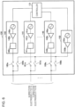
- the individual X-direction electrodes 11 to 15 and the individual Y-direction electrodes 21 to 25 are connected to a driving detection unit 130 as illustrated in Fig. 5 , and AC voltage is applied to the individual X-direction electrodes 11 to 15 and the individual Y-direction electrodes 21 to 25.
- the driving detection unit 130 includes a controller 131, a plurality of detection circuits 140 to 149, and a shield driving circuit 150.
- the detection circuits 140 to 149 individually apply AC voltage to a selected number of the X-direction electrodes 11 to 15 and the Y-direction electrodes 21 to 25 and measure supplied current.
- the shield driving circuit 150 applies AC voltage to the others of the X-direction electrodes 11 to 15 and the Y-direction electrodes 21 to 25 which are not selected.
- the detection circuit 140 includes an alternating-current source 140a, an amplifier 140b, and an ammeter 140c.
- the amplifier 140b amplifies alternating current generated in the alternating-current source 140a to obtain a desired amplitude and supplies the amplified alternating current through the ammeter 140c.
- the amplifiers 141b to 149b amplify alternating current generated in the corresponding alternating-current sources 141a to 149a to obtain desired amplitudes and supply the amplified alternating current through the corresponding ammeters 141c to 149c.
- the ammeters 140c to 149c are referred to as current measurement units where appropriate.
- the detection circuits 140 to 149 are not limited to this configuration and charge amplifiers using operational amplifiers may be used.
- the shield driving circuit 150 includes an alternating-current source 150a and an amplifier 150b which amplifies alternating current generated in the alternating-current source 150a to obtain desired amplitude and supplies the amplified alternating current.
- the alternating current generated in the alternating-current sources 140a to 149a and the alternating current generated in the alternating-current source 150a have the same frequency and the same phase.
- the alternating-current sources 140a to 149a are referred to as first alternating-current sources, and the alternating-current source 150a is referred to as a second alternating-current source where appropriate.
- the X-direction electrodes 11 to 15 and the Y-direction electrodes 21 to 25 are connected to the driving detection unit 130, and the driving detection unit 130 includes switches for connecting the electrodes to the detection circuits 140 to 149 or the shield driving circuit 150.
- the driving detection unit 130 includes switches 160a to 169a for connection between the electrodes to the detection circuits 140 to 149 and switches 160b to 169b for connection between the electrodes to the shield driving circuit 150.
- the switches 160a and 160b are connected to the X-direction electrode 11, the detection circuit 140 is connected to the switch 160a, and the shield driving circuit 150 is connected to the switch 160b.
- the switch 160a is closed, the X-direction electrode 11 is electrically connected to the detection circuit 140, the detection circuit 140 applies AC voltage, and the ammeter 140c measures current to be supplied to the X-direction electrode 11.
- the switch 160b is opened.
- the X-direction electrodes 11 to 15 are connected to the corresponding five of the detection circuits 140, 141, and so on, and the Y-direction electrodes 21 to 25 are connected to the shield driving circuit 150. In this state, alternating voltage is applied to the X-direction electrodes 11 to 15 and furthermore, alternating voltage is also applied to the Y-direction electrodes 21 to 25.
- Fig. 8 is a cross-sectional view taken along a dashed-dotted line 7A to 7B in Fig. 7 .
- alternating voltage is applied to the X-direction electrodes 11 to 15 and the Y-direction electrodes 21 to 25, and electric lines of force are generated in a substantially vertical direction relative to planes of the X-direction electrodes 12 and so on and the Y-direction electrodes 21, 22, and so on as illustrated by a dotted line in Fig. 8 .
- electric fields are generated both in the X-direction electrodes 11 to 15 and the Y-direction electrodes 21 to 25, and therefore, when the finger 100 or the like approaches the touch sensor, a capacitance is generated between the finger 100 or the like and electrode patterns and a largest amount of current is supplied to an electrode having an electrode pattern positioned closest to the finger 100 or the like.
- a position of a Y coordinate of the finger 100 or the like may be specified by specifying one of the X-direction electrodes 11 to 15 which receives a largest amount of current.
- the touch sensor according to this embodiment has higher density of electric lines of force and attains improved detection sensitivity, when compared with the touch sensor illustrated in Fig. 1 . Furthermore, a larger number of electric lines of force in the Z direction are generated relative to the diamond-shaped electrode patterns of the X-direction electrodes 11 to 15 and the diamond-shaped electrode patterns of the Y-direction electrodes 21 to 25, and therefore, directivity and accuracy of a detection position may be improved.
- the touch sensor according to this embodiment has higher sensitivity and higher directivity and more effectively avoid false detection caused by water.
- a result is illustrated in Table 1.
- Table 1 Sensitivity Directivity Suppression of False Detection due to Water Touch Sensor of First Embodiment High High High Touch Sensor Having Configuration of Fig. 1 Low Low Low
- a method for driving a touch sensor according to a second embodiment will be described.
- a method for driving the touch sensor illustrated in Fig. 5 which is employed in a case where the number of driving circuits is smaller than the number of X-direction electrodes or Y-direction electrodes is illustrated.
- the number of X-direction electrodes 11 to 15 is 5, the number of Y-direction electrodes 21 to 25 is 5, and the number of driving circuits included in a controller is 4 will be described as an example.
- the driving electrodes may not be simultaneously connected to the X-direction electrodes 11 to 15, and the driving electrodes may not be simultaneously connected to the Y-direction electrodes 21 to 25.
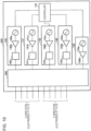
- a driving detection unit 230 includes four detection circuits 140 to 143, the number of detection circuits 140 to 143 being smaller than the number of X-direction electrodes 11 to 15 or the number of the Y-direction electrodes 21 to 25, and a shield driving circuit 150.
- the driving detection unit 230 includes a controller 131 which controls various operations in the driving detection unit 230.
- the driving detection unit 230 includes a selector 260, and lines of the X-direction electrodes 11 to 15 and the Y-direction electrodes 21 to 25 connected to the driving detection unit 230 are connected to the selector 260 included in the driving detection unit 230. Furthermore, the detection circuits 140 to 143 and the shield driving circuit 150 are connected to the selector 260 which selectively connects the X-direction electrodes 11 to 15 and the Y-direction electrodes 21 to 25 to the detection circuits 140 to 143 and the shield driving circuit 150. Specifically, electrodes selected from among the X-direction electrodes 11 to 15 and the Y-direction electrodes 21 to 25 are connected to the detection circuits 140 to 143 and the other electrodes which are not selected are connected to the shield driving circuit 150.
- the selector 260 connects the X-direction electrode 11 to the detection circuit 140, the X-direction electrode 12 to the detection circuit 141, the X-direction electrode 13 to the detection circuit 142, the X-direction electrode 12 to the detection circuit 143, and the X-direction electrode 15 and the Y-direction electrodes 21 to 25 to the shield driving circuit 150.
- alternating voltage is applied to the X-direction electrodes 11 to 15 and the Y-direction electrodes 21 to 25, and the X-direction electrodes 11 to 14 connected to the detection circuits 140 to 143 may measure current supplied to the X-direction electrodes 11 to 14 using ammeters 140c to 143c included in the detection circuits 140 to 143, respectively.
- the selector 260 connects the X-direction electrode 15 to the detection circuit 140, the Y-direction electrode 21 to the detection circuit 141, the Y-direction electrode 22 to the detection circuit 142, the Y-direction electrode 23 to the detection circuit 143, and the X-direction electrodes 11 to 14 and the Y-direction electrodes 24 and 25 to the shield driving circuit 150.
- alternating voltage is applied to the X-direction electrodes 11 to 15 and the Y-direction electrodes 21 to 25, and the X-direction electrode 15 and the Y-direction electrodes 21 to 23 which are connected to the detection circuits 140 to 143 may measure current supplied to the X-direction electrode 15 and the Y-direction electrodes 21 to 23 using the ammeters 140c to 143c included in the detection circuits 140 to 143, respectively.
- the selector 260 connects the Y-direction electrode 24 to the detection circuit 140, the Y-direction electrode 25 to the detection circuit 141, and the X-direction electrodes 11 to 15 and the Y-direction electrodes 21 to 23 to the shield driving circuit 150.
- alternating voltage is applied to the X-direction electrodes 11 to 15 and the Y-direction electrodes 21 to 25, and the Y-direction electrodes 24 and 25 connected to the detection circuits 140 and 141 may measure current supplied to the Y-direction electrodes 24 to 25 using the ammeters 140c and 141c included in the detection circuits 140 and 141, respectively.
- the driving detection unit 230 performs switching of connections using the selector 260 under control of the controller 131 so that electrodes to be connected to the detection circuits are successively selected from among the X-direction electrodes 11 to 15 and the Y-direction electrodes 21 to 25 and the selected electrodes are connected to the detection circuits.
- an X-direction electrode which receives a largest amount of current is selected from among the X-direction electrodes 11 to 15, and a Y-direction electrode which receives a largest amount of current is selected from among the Y-direction electrodes 21 to 25 so that a two-dimensional position of a finger 100 or the like may be detected. Accordingly, in this embodiment, even when the number of detection circuits is smaller than the number of X-direction electrodes or the number of Y-direction electrodes, a movement of the finger 100 or the like may be obtained.
- a touch sensor according to a third embodiment will be described.
- the touch sensor of this embodiment corresponds to the touch sensor illustrated in Fig. 5 , and as illustrated in Fig. 14 , a driving detection unit 330 includes detection circuits 140 to 149 corresponding to the number of X-direction electrodes 11 to 15 and the number of Y-direction electrodes 21 to 25.
- the detection circuits 140 to 149 corresponding to the X-direction electrodes 11 to 15 and the Y-direction electrodes 21 to 25 are respectively connected to the X-direction electrodes 11 to 15 and the Y-direction electrodes 21 to 25, and alternating voltage is applied to the X-direction electrodes 11 to 15 and the Y-direction electrodes 21 to 25 from the detection circuits 140 to 149. Therefore, a shield driving circuit is not provided according to this embodiment.
- Fig. 15 all the X-direction electrodes 11 to 15 and the Y-direction electrodes 21 to 25 are connected to the corresponding detection circuits 140 to 149, and therefore, position detection using the X-direction electrodes 11 to 15 and position detection using the Y-direction electrodes 21 to 25 may be simultaneously performed. Accordingly, although the number of detection circuits is large, switches and a shield driving circuit are not required.
- a touch sensor according to a fourth embodiment will be described.
- the touch sensor illustrated in Fig. 5 is used, and amplitude of alternating voltage supplied from a shield driving circuit 150 is larger than amplitude of alternating voltage supplied from the detection circuits 140 to 149.
- Such control of alternating voltage may be performed by a controller 131 included in a driving detection unit 130.
- Fig. 16 is a cross-sectional view taken along a dashed-dotted line 15A to 15B in Fig. 15 .
- a touch sensor which is an electrostatic sensor according to a fifth embodiment will be described.
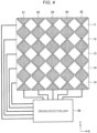
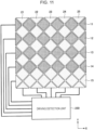
- X-direction electrodes 11 to 15 and Y-direction electrodes 21 to 25 are disposed on one surface 410a, which is a front surface, of an insulating body substrate 410, and a shield electrode 420 is disposed on the other surface 410b which is the other side of the surface 410a as illustrated in Fig. 17 and 18 .
- Fig. 18 is a cross-sectional view taken along a dashed-dotted line 17A to 17B in Fig. 17 .
- the shield electrode 420 is formed so as to cover the entire surface 410b of the insulating body substrate 410 and covers the X-direction electrodes 11 to 15 and the Y-direction electrodes 21 to 25 from a back surface. Specifically, in a plan view in a Z direction, the X-direction electrodes 11 to 15 and the Y-direction electrodes 21 to 25 are included in a region in which the shield electrode 420 is disposed.
- the shield electrode 420 is connected to a shield driving circuit 150 of a driving detection unit 130 and alternating voltage is applied to the shield electrode 420.
- the shield electrode 420 is disposed and alternating voltage is applied by the shield driving circuit 150, an adverse effect of noise from the back side, that is, an adverse effect of noise generated on a side in which the shield electrode 420 is disposed, on the X-direction electrodes 11 to 15 and the Y-direction electrodes 21 to 25 may be suppressed.
Landscapes
- Engineering & Computer Science (AREA)
- General Engineering & Computer Science (AREA)
- Theoretical Computer Science (AREA)
- Physics & Mathematics (AREA)
- General Physics & Mathematics (AREA)
- Human Computer Interaction (AREA)
- Position Input By Displaying (AREA)
Claims (4)
- Elektrostatischer Sensor zum Erfassen einer Position eines zu erfassenden Objekts, das sich dem elektrostatischen Sensor nähert, aufweisend:eine erste Elektrodengruppe (11-15), die eine Mehrzahl von Elektroden aufweist, die in einer ersten Richtung angeordnet sind;eine zweite Elektrodengruppe (21-25), die eine Mehrzahl von Elektroden aufweist, die in einer zu der ersten Richtung orthogonalen, zweiten Richtung angeordnet sind;Erfassungsschaltungen (140-149), die dazu ausgebildet sind, einzeln mit Elektroden verbunden zu werden, die aus den Elektroden der ersten Elektrodengruppe (11-15) und den Elektroden der zweiten Elektrodengruppe (140-149) ausgewählt werden, wobei jede Erfassungsschaltung (140-149) eine erste Wechselstromquelle und eine Strommesseinheit (140c-149c) besitzt;eine zweite Wechselstromquelle (150a), die dazu ausgebildet ist, mit nicht ausgewählten Elektroden unter den Elektroden der ersten Elektrodengruppe (11-15) und den Elektroden der zweiten Elektrodengruppe (21-25) verbunden zu werden,wobei:die erste Wechselstromquelle (140a-149a) und die zweite Wechselstromquelle (150a) dazu ausgebildet sind, eine erste Wechselspannung bzw. eine zweite Wechselspannung zu erzeugen, die die gleiche Frequenz und die gleiche Phase aufweisen, undder elektrostatische Sensor ferner eine Steuerung (131) aufweist, die dazu ausgebildet ist:nacheinander und wiederholt mit den Erfassungsschaltungen (140-149) zu verbindende Elektroden aus den Elektroden der ersten Elektrodengruppe (11-15) und den Elektroden der zweiten Elektrodengruppe (21-25) auszuwählen, so dass die ausgewählten Elektroden mit den Erfassungsschaltungen (140-149) verbunden werden und die nicht ausgewählten Elektroden mit der zweiten Wechselstromquelle (150a) verbunden werden, und dass die erste Wechselspannung und die zweite Wechselspannung an die ausgewählten Elektroden bzw. die nicht ausgewählten Elektroden zu einem Zeitpunkt angelegt werden, so dass von den ausgewählten Elektroden keine elektrische Kraftlinien in Richtung auf die nicht ausgewählten Elektroden erzeugt werden, undeine Position des zu erfassenden Objekts auf der Basis von Strom zu erfassen, der von in den Erfassungsschaltungen (140-149) enthaltenen Strommesseinheiten (140c-149c) erfasst wird,dadurch gekennzeichnet,dass die Elektroden der ersten Elektrodengruppe (11-15) und die Elektroden der zweiten Elektrodengruppe (21-25) auf der einen Oberfläche eines Isolierkörpersubstrats (410) angeordnet sind,dass eine Abschirmelektrode (420) auf der anderen Oberfläche des Isolierkörpersubstrats (410) angeordnet ist, unddass die zweite Wechselstromquelle (150a) dazu ausgebildet ist, die zweite Wechselspannung an die Abschirmelektrode (420) anzulegen.
- Elektrostatischer Sensor nach Anspruch 1,
wobei die erste Wechselspannung und die zweite Wechselspannung die gleiche Spannungsamplitude aufweisen. - Elektrostatischer Sensor nach Anspruch 1,
wobei die Amplitude der ersten Wechselspannung kleiner ist als die Amplitude der zweiten Wechselspannung. - Elektrostatischer Sensor nach einem der Ansprüche 1 bis 3,
wobei die Anzahl der Erfassungsschaltungen (140-149) kleiner ist als die Anzahl der Elektroden der ersten Elektrodengruppe (11-15) oder die Anzahl der Elektroden der zweiten Elektrodengruppe (21-25).
Applications Claiming Priority (2)
| Application Number | Priority Date | Filing Date | Title |
|---|---|---|---|
| JP2017243986 | 2017-12-20 | ||
| PCT/JP2018/044539 WO2019124054A1 (ja) | 2017-12-20 | 2018-12-04 | 静電センサ |
Publications (3)
| Publication Number | Publication Date |
|---|---|
| EP3731071A1 EP3731071A1 (de) | 2020-10-28 |
| EP3731071A4 EP3731071A4 (de) | 2021-08-18 |
| EP3731071B1 true EP3731071B1 (de) | 2024-10-23 |
Family
ID=66993652
Family Applications (1)
| Application Number | Title | Priority Date | Filing Date |
|---|---|---|---|
| EP18891576.3A Active EP3731071B1 (de) | 2017-12-20 | 2018-12-04 | Elektrostatischer sensor |
Country Status (6)
| Country | Link |
|---|---|
| US (1) | US11131566B2 (de) |
| EP (1) | EP3731071B1 (de) |
| JP (1) | JP6894984B2 (de) |
| KR (1) | KR102309643B1 (de) |
| CN (1) | CN111492333B (de) |
| WO (1) | WO2019124054A1 (de) |
Citations (1)
| Publication number | Priority date | Publication date | Assignee | Title |
|---|---|---|---|---|
| US20170003816A1 (en) * | 2009-07-10 | 2017-01-05 | Apple Inc. | Touch and hover sensing |
Family Cites Families (22)
| Publication number | Priority date | Publication date | Assignee | Title |
|---|---|---|---|---|
| JPS6038368B2 (ja) | 1981-09-12 | 1985-08-31 | 日東電工株式会社 | 貼付剤の製造方法 |
| US5540085A (en) * | 1993-11-30 | 1996-07-30 | Sakata Denki Co., Ltd | Method of measuring leakage position in impervious bottom sheet using electrodes mounted on both surfaces of the sheet and apparatus therefor |
| JP3394187B2 (ja) * | 1997-08-08 | 2003-04-07 | シャープ株式会社 | 座標入力装置および表示一体型座標入力装置 |
| JP5372630B2 (ja) | 2008-07-17 | 2013-12-18 | Nltテクノロジー株式会社 | 表示装置及び表示装置の駆動方法 |
| JP2010061405A (ja) * | 2008-09-03 | 2010-03-18 | Rohm Co Ltd | 静電容量センサ、その検出回路、入力装置および容量センサの制御方法 |
| DE102009046177A1 (de) * | 2008-10-30 | 2010-06-10 | Samsung Electronics Co., Ltd., Suwon | Berührungsdatengenerator |
| KR101573698B1 (ko) * | 2009-03-18 | 2015-12-03 | 삼성전자주식회사 | 터치 데이터 프로세싱 회로, 이를 포함하는 디스플레이 구동 회로 및 디스플레이 장치 |
| JP5267932B2 (ja) * | 2008-11-11 | 2013-08-21 | 株式会社フジクラ | 位置検出装置 |
| JP2011128896A (ja) * | 2009-12-17 | 2011-06-30 | Smk Corp | 静電容量式タッチパネルとその製造方法 |
| CN102375587B (zh) | 2010-08-15 | 2015-03-11 | 宸鸿科技(厦门)有限公司 | 侦测多触摸点的真坐标的触控面板及侦测方法 |
| JP2012059073A (ja) * | 2010-09-09 | 2012-03-22 | Bridgestone Corp | 情報表示装置 |
| US9016198B2 (en) * | 2010-10-05 | 2015-04-28 | Hewlett-Packard Development Company, L.P. | Printers, methods, and apparatus to filter imaging oil |
| JP2012221013A (ja) * | 2011-04-05 | 2012-11-12 | Alps Electric Co Ltd | 座標検出装置 |
| JP2013246557A (ja) * | 2012-05-24 | 2013-12-09 | Asahi Kasei Electronics Co Ltd | タッチセンサの信号処理回路、およびタッチセンサ |
| JP5984259B2 (ja) * | 2012-09-20 | 2016-09-06 | 株式会社ワコム | 位置検出装置 |
| JP6311223B2 (ja) * | 2013-06-07 | 2018-04-18 | 日本電産リード株式会社 | 検査装置、検査装置のキャリブレーション方法及び検査方法 |
| JP2015195010A (ja) * | 2014-03-20 | 2015-11-05 | パナソニックIpマネジメント株式会社 | タッチセンサ機能を有する入力装置および表示装置 |
| JP6304814B2 (ja) * | 2014-05-23 | 2018-04-04 | 株式会社ワコム | 位置検出装置及び位置指示器 |
| JP6406697B2 (ja) * | 2014-09-17 | 2018-10-17 | 株式会社ワコム | 位置検出装置及び位置検出方法 |
| JP6038368B2 (ja) | 2016-03-08 | 2016-12-07 | 三菱電機株式会社 | タッチパネルおよび表示装置 |
| JP6695711B2 (ja) * | 2016-03-10 | 2020-05-20 | 株式会社ジャパンディスプレイ | 表示装置及び表示装置のタッチ検出方法 |
| TWI643113B (zh) * | 2017-03-03 | 2018-12-01 | 日商阿爾普士電氣股份有限公司 | Input device and control method thereof |
-
2018
- 2018-12-04 EP EP18891576.3A patent/EP3731071B1/de active Active
- 2018-12-04 CN CN201880081959.9A patent/CN111492333B/zh active Active
- 2018-12-04 JP JP2019560936A patent/JP6894984B2/ja active Active
- 2018-12-04 KR KR1020207017191A patent/KR102309643B1/ko active Active
- 2018-12-04 WO PCT/JP2018/044539 patent/WO2019124054A1/ja not_active Ceased
-
2020
- 2020-06-16 US US16/902,905 patent/US11131566B2/en active Active
Patent Citations (1)
| Publication number | Priority date | Publication date | Assignee | Title |
|---|---|---|---|---|
| US20170003816A1 (en) * | 2009-07-10 | 2017-01-05 | Apple Inc. | Touch and hover sensing |
Also Published As
| Publication number | Publication date |
|---|---|
| WO2019124054A1 (ja) | 2019-06-27 |
| CN111492333B (zh) | 2023-08-04 |
| CN111492333A (zh) | 2020-08-04 |
| JPWO2019124054A1 (ja) | 2020-09-24 |
| EP3731071A4 (de) | 2021-08-18 |
| KR20200087819A (ko) | 2020-07-21 |
| JP6894984B2 (ja) | 2021-06-30 |
| US11131566B2 (en) | 2021-09-28 |
| KR102309643B1 (ko) | 2021-10-06 |
| US20200309570A1 (en) | 2020-10-01 |
| EP3731071A1 (de) | 2020-10-28 |
Similar Documents
| Publication | Publication Date | Title |
|---|---|---|
| CN103324368B (zh) | 位置检测装置 | |
| KR102257173B1 (ko) | 감소된 기생 커패시턴스를 위한 변조된 전력 공급부 | |
| US4929934A (en) | Pressure-sensitive input apparatus | |
| KR101572866B1 (ko) | 터치 디스플레이 장치 | |
| CN112214124B (zh) | 处理系统、输入装置及用于检测输入信号的方法 | |
| US9134396B2 (en) | Reducing bending effects in touch sensor devices | |
| JP7190347B2 (ja) | ペンが送信したペン信号を検出するためのセンサ | |
| US9740347B2 (en) | Active pen sensing for a display device having an integrated sensing device | |
| US9690435B2 (en) | Touch display panel and method for manufacturing and driving the same and touch display device | |
| US20150138144A1 (en) | Coordinate input device and mobile terminal | |
| US10503320B2 (en) | Active feedforward interference cancellation techniques for sensor analog front-end | |
| US20150062075A1 (en) | Capacitive input device | |
| US20160328079A1 (en) | Force sensor substrate | |
| KR20090039648A (ko) | 화면 입력형 화상 표시 시스템 | |
| KR20160064224A (ko) | 이미지 터치 센싱을 위한 매트릭스 센서 | |
| US20190171319A1 (en) | Display device with built-in touch sensor, and drive method thereof | |
| US9946404B1 (en) | LED screen noise sensing for discreet capacitive sensors | |
| US20150220206A1 (en) | Display noise cancellation | |
| JP2017528803A5 (de) | ||
| CN104199588B (zh) | 一种触摸屏及触控显示装置 | |
| US11003288B2 (en) | Active input sensing using regional scanning | |
| WO2024041967A1 (en) | Touch-sensitive system and method | |
| US20120154325A1 (en) | Touchscreen panel | |
| EP3731071B1 (de) | Elektrostatischer sensor | |
| US11726609B2 (en) | Touch-sensitive apparatus and method |
Legal Events
| Date | Code | Title | Description |
|---|---|---|---|
| STAA | Information on the status of an ep patent application or granted ep patent |
Free format text: STATUS: THE INTERNATIONAL PUBLICATION HAS BEEN MADE |
|
| PUAI | Public reference made under article 153(3) epc to a published international application that has entered the european phase |
Free format text: ORIGINAL CODE: 0009012 |
|
| STAA | Information on the status of an ep patent application or granted ep patent |
Free format text: STATUS: REQUEST FOR EXAMINATION WAS MADE |
|
| 17P | Request for examination filed |
Effective date: 20200709 |
|
| AK | Designated contracting states |
Kind code of ref document: A1 Designated state(s): AL AT BE BG CH CY CZ DE DK EE ES FI FR GB GR HR HU IE IS IT LI LT LU LV MC MK MT NL NO PL PT RO RS SE SI SK SM TR |
|
| AX | Request for extension of the european patent |
Extension state: BA ME |
|
| DAV | Request for validation of the european patent (deleted) | ||
| DAX | Request for extension of the european patent (deleted) | ||
| A4 | Supplementary search report drawn up and despatched |
Effective date: 20210716 |
|
| RIC1 | Information provided on ipc code assigned before grant |
Ipc: G06F 3/041 20060101AFI20210712BHEP Ipc: G06F 3/044 20060101ALI20210712BHEP |
|
| STAA | Information on the status of an ep patent application or granted ep patent |
Free format text: STATUS: EXAMINATION IS IN PROGRESS |
|
| 17Q | First examination report despatched |
Effective date: 20220310 |
|
| GRAP | Despatch of communication of intention to grant a patent |
Free format text: ORIGINAL CODE: EPIDOSNIGR1 |
|
| STAA | Information on the status of an ep patent application or granted ep patent |
Free format text: STATUS: GRANT OF PATENT IS INTENDED |
|
| RIC1 | Information provided on ipc code assigned before grant |
Ipc: G01D 5/24 20060101ALI20240506BHEP Ipc: G06F 3/044 20060101ALI20240506BHEP Ipc: G06F 3/041 20060101AFI20240506BHEP |
|
| INTG | Intention to grant announced |
Effective date: 20240522 |
|
| GRAS | Grant fee paid |
Free format text: ORIGINAL CODE: EPIDOSNIGR3 |
|
| GRAA | (expected) grant |
Free format text: ORIGINAL CODE: 0009210 |
|
| STAA | Information on the status of an ep patent application or granted ep patent |
Free format text: STATUS: THE PATENT HAS BEEN GRANTED |
|
| AK | Designated contracting states |
Kind code of ref document: B1 Designated state(s): AL AT BE BG CH CY CZ DE DK EE ES FI FR GB GR HR HU IE IS IT LI LT LU LV MC MK MT NL NO PL PT RO RS SE SI SK SM TR |
|
| REG | Reference to a national code |
Ref country code: GB Ref legal event code: FG4D |
|
| REG | Reference to a national code |
Ref country code: CH Ref legal event code: EP |
|
| REG | Reference to a national code |
Ref country code: DE Ref legal event code: R096 Ref document number: 602018075851 Country of ref document: DE |
|
| REG | Reference to a national code |
Ref country code: IE Ref legal event code: FG4D |
|
| REG | Reference to a national code |
Ref country code: LT Ref legal event code: MG9D |
|
| REG | Reference to a national code |
Ref country code: NL Ref legal event code: MP Effective date: 20241023 |
|
| REG | Reference to a national code |
Ref country code: AT Ref legal event code: MK05 Ref document number: 1735369 Country of ref document: AT Kind code of ref document: T Effective date: 20241023 |
|
| PG25 | Lapsed in a contracting state [announced via postgrant information from national office to epo] |
Ref country code: NL Free format text: LAPSE BECAUSE OF FAILURE TO SUBMIT A TRANSLATION OF THE DESCRIPTION OR TO PAY THE FEE WITHIN THE PRESCRIBED TIME-LIMIT Effective date: 20241023 |
|
| PG25 | Lapsed in a contracting state [announced via postgrant information from national office to epo] |
Ref country code: NL Free format text: LAPSE BECAUSE OF FAILURE TO SUBMIT A TRANSLATION OF THE DESCRIPTION OR TO PAY THE FEE WITHIN THE PRESCRIBED TIME-LIMIT Effective date: 20241023 |
|
| PG25 | Lapsed in a contracting state [announced via postgrant information from national office to epo] |
Ref country code: IS Free format text: LAPSE BECAUSE OF FAILURE TO SUBMIT A TRANSLATION OF THE DESCRIPTION OR TO PAY THE FEE WITHIN THE PRESCRIBED TIME-LIMIT Effective date: 20250223 Ref country code: HR Free format text: LAPSE BECAUSE OF FAILURE TO SUBMIT A TRANSLATION OF THE DESCRIPTION OR TO PAY THE FEE WITHIN THE PRESCRIBED TIME-LIMIT Effective date: 20241023 Ref country code: PT Free format text: LAPSE BECAUSE OF FAILURE TO SUBMIT A TRANSLATION OF THE DESCRIPTION OR TO PAY THE FEE WITHIN THE PRESCRIBED TIME-LIMIT Effective date: 20250224 |
|
| PG25 | Lapsed in a contracting state [announced via postgrant information from national office to epo] |
Ref country code: FI Free format text: LAPSE BECAUSE OF FAILURE TO SUBMIT A TRANSLATION OF THE DESCRIPTION OR TO PAY THE FEE WITHIN THE PRESCRIBED TIME-LIMIT Effective date: 20241023 |
|
| PG25 | Lapsed in a contracting state [announced via postgrant information from national office to epo] |
Ref country code: BG Free format text: LAPSE BECAUSE OF FAILURE TO SUBMIT A TRANSLATION OF THE DESCRIPTION OR TO PAY THE FEE WITHIN THE PRESCRIBED TIME-LIMIT Effective date: 20241023 |
|
| PG25 | Lapsed in a contracting state [announced via postgrant information from national office to epo] |
Ref country code: ES Free format text: LAPSE BECAUSE OF FAILURE TO SUBMIT A TRANSLATION OF THE DESCRIPTION OR TO PAY THE FEE WITHIN THE PRESCRIBED TIME-LIMIT Effective date: 20241023 |
|
| PG25 | Lapsed in a contracting state [announced via postgrant information from national office to epo] |
Ref country code: NO Free format text: LAPSE BECAUSE OF FAILURE TO SUBMIT A TRANSLATION OF THE DESCRIPTION OR TO PAY THE FEE WITHIN THE PRESCRIBED TIME-LIMIT Effective date: 20250123 |
|
| PG25 | Lapsed in a contracting state [announced via postgrant information from national office to epo] |
Ref country code: LV Free format text: LAPSE BECAUSE OF FAILURE TO SUBMIT A TRANSLATION OF THE DESCRIPTION OR TO PAY THE FEE WITHIN THE PRESCRIBED TIME-LIMIT Effective date: 20241023 Ref country code: AT Free format text: LAPSE BECAUSE OF FAILURE TO SUBMIT A TRANSLATION OF THE DESCRIPTION OR TO PAY THE FEE WITHIN THE PRESCRIBED TIME-LIMIT Effective date: 20241023 Ref country code: GR Free format text: LAPSE BECAUSE OF FAILURE TO SUBMIT A TRANSLATION OF THE DESCRIPTION OR TO PAY THE FEE WITHIN THE PRESCRIBED TIME-LIMIT Effective date: 20250124 |
|
| PG25 | Lapsed in a contracting state [announced via postgrant information from national office to epo] |
Ref country code: PL Free format text: LAPSE BECAUSE OF FAILURE TO SUBMIT A TRANSLATION OF THE DESCRIPTION OR TO PAY THE FEE WITHIN THE PRESCRIBED TIME-LIMIT Effective date: 20241023 |
|
| PG25 | Lapsed in a contracting state [announced via postgrant information from national office to epo] |
Ref country code: RS Free format text: LAPSE BECAUSE OF FAILURE TO SUBMIT A TRANSLATION OF THE DESCRIPTION OR TO PAY THE FEE WITHIN THE PRESCRIBED TIME-LIMIT Effective date: 20250123 |
|
| PG25 | Lapsed in a contracting state [announced via postgrant information from national office to epo] |
Ref country code: SM Free format text: LAPSE BECAUSE OF FAILURE TO SUBMIT A TRANSLATION OF THE DESCRIPTION OR TO PAY THE FEE WITHIN THE PRESCRIBED TIME-LIMIT Effective date: 20241023 |
|
| PG25 | Lapsed in a contracting state [announced via postgrant information from national office to epo] |
Ref country code: MC Free format text: LAPSE BECAUSE OF FAILURE TO SUBMIT A TRANSLATION OF THE DESCRIPTION OR TO PAY THE FEE WITHIN THE PRESCRIBED TIME-LIMIT Effective date: 20241023 |
|
| PG25 | Lapsed in a contracting state [announced via postgrant information from national office to epo] |
Ref country code: DK Free format text: LAPSE BECAUSE OF FAILURE TO SUBMIT A TRANSLATION OF THE DESCRIPTION OR TO PAY THE FEE WITHIN THE PRESCRIBED TIME-LIMIT Effective date: 20241023 |
|
| PG25 | Lapsed in a contracting state [announced via postgrant information from national office to epo] |
Ref country code: EE Free format text: LAPSE BECAUSE OF FAILURE TO SUBMIT A TRANSLATION OF THE DESCRIPTION OR TO PAY THE FEE WITHIN THE PRESCRIBED TIME-LIMIT Effective date: 20241023 |
|
| PG25 | Lapsed in a contracting state [announced via postgrant information from national office to epo] |
Ref country code: RO Free format text: LAPSE BECAUSE OF FAILURE TO SUBMIT A TRANSLATION OF THE DESCRIPTION OR TO PAY THE FEE WITHIN THE PRESCRIBED TIME-LIMIT Effective date: 20241023 |
|
| REG | Reference to a national code |
Ref country code: DE Ref legal event code: R097 Ref document number: 602018075851 Country of ref document: DE |
|
| PG25 | Lapsed in a contracting state [announced via postgrant information from national office to epo] |
Ref country code: SK Free format text: LAPSE BECAUSE OF FAILURE TO SUBMIT A TRANSLATION OF THE DESCRIPTION OR TO PAY THE FEE WITHIN THE PRESCRIBED TIME-LIMIT Effective date: 20241023 |
|
| PG25 | Lapsed in a contracting state [announced via postgrant information from national office to epo] |
Ref country code: CZ Free format text: LAPSE BECAUSE OF FAILURE TO SUBMIT A TRANSLATION OF THE DESCRIPTION OR TO PAY THE FEE WITHIN THE PRESCRIBED TIME-LIMIT Effective date: 20241023 |
|
| PG25 | Lapsed in a contracting state [announced via postgrant information from national office to epo] |
Ref country code: IT Free format text: LAPSE BECAUSE OF FAILURE TO SUBMIT A TRANSLATION OF THE DESCRIPTION OR TO PAY THE FEE WITHIN THE PRESCRIBED TIME-LIMIT Effective date: 20241023 |
|
| REG | Reference to a national code |
Ref country code: CH Ref legal event code: PL |
|
| PG25 | Lapsed in a contracting state [announced via postgrant information from national office to epo] |
Ref country code: LU Free format text: LAPSE BECAUSE OF NON-PAYMENT OF DUE FEES Effective date: 20241204 |
|
| PLBE | No opposition filed within time limit |
Free format text: ORIGINAL CODE: 0009261 |
|
| STAA | Information on the status of an ep patent application or granted ep patent |
Free format text: STATUS: NO OPPOSITION FILED WITHIN TIME LIMIT |
|
| PG25 | Lapsed in a contracting state [announced via postgrant information from national office to epo] |
Ref country code: SE Free format text: LAPSE BECAUSE OF FAILURE TO SUBMIT A TRANSLATION OF THE DESCRIPTION OR TO PAY THE FEE WITHIN THE PRESCRIBED TIME-LIMIT Effective date: 20241023 |
|
| 26N | No opposition filed |
Effective date: 20250724 |
|
| REG | Reference to a national code |
Ref country code: BE Ref legal event code: MM Effective date: 20241231 |
|
| PG25 | Lapsed in a contracting state [announced via postgrant information from national office to epo] |
Ref country code: BE Free format text: LAPSE BECAUSE OF NON-PAYMENT OF DUE FEES Effective date: 20241231 |
|
| PG25 | Lapsed in a contracting state [announced via postgrant information from national office to epo] |
Ref country code: CH Free format text: LAPSE BECAUSE OF NON-PAYMENT OF DUE FEES Effective date: 20241231 |
|
| PG25 | Lapsed in a contracting state [announced via postgrant information from national office to epo] |
Ref country code: IE Free format text: LAPSE BECAUSE OF NON-PAYMENT OF DUE FEES Effective date: 20241204 |
|
| PGFP | Annual fee paid to national office [announced via postgrant information from national office to epo] |
Ref country code: DE Payment date: 20251211 Year of fee payment: 8 |
|
| PGFP | Annual fee paid to national office [announced via postgrant information from national office to epo] |
Ref country code: GB Payment date: 20251219 Year of fee payment: 8 |
|
| PGFP | Annual fee paid to national office [announced via postgrant information from national office to epo] |
Ref country code: FR Payment date: 20251229 Year of fee payment: 8 |