EP3726531A2 - Verfahren und system zum schreiben in und lesen aus einer speichervorrichtung - Google Patents
Verfahren und system zum schreiben in und lesen aus einer speichervorrichtung Download PDFInfo
- Publication number
- EP3726531A2 EP3726531A2 EP20167847.1A EP20167847A EP3726531A2 EP 3726531 A2 EP3726531 A2 EP 3726531A2 EP 20167847 A EP20167847 A EP 20167847A EP 3726531 A2 EP3726531 A2 EP 3726531A2
- Authority
- EP
- European Patent Office
- Prior art keywords
- computer
- implemented method
- voltage
- asic
- data
- Prior art date
- Legal status (The legal status is an assumption and is not a legal conclusion. Google has not performed a legal analysis and makes no representation as to the accuracy of the status listed.)
- Pending
Links
Images




Classifications
-
- G—PHYSICS
- G11—INFORMATION STORAGE
- G11C—STATIC STORES
- G11C11/00—Digital stores characterised by the use of particular electric or magnetic storage elements; Storage elements therefor
- G11C11/56—Digital stores characterised by the use of particular electric or magnetic storage elements; Storage elements therefor using storage elements with more than two stable states represented by steps, e.g. of voltage, current, phase, frequency
-
- G—PHYSICS
- G11—INFORMATION STORAGE
- G11C—STATIC STORES
- G11C11/00—Digital stores characterised by the use of particular electric or magnetic storage elements; Storage elements therefor
- G11C11/21—Digital stores characterised by the use of particular electric or magnetic storage elements; Storage elements therefor using electric elements
- G11C11/22—Digital stores characterised by the use of particular electric or magnetic storage elements; Storage elements therefor using electric elements using ferroelectric elements
- G11C11/225—Auxiliary circuits
- G11C11/2275—Writing or programming circuits or methods
-
- G—PHYSICS
- G11—INFORMATION STORAGE
- G11C—STATIC STORES
- G11C17/00—Read-only memories programmable only once; Semi-permanent stores, e.g. manually-replaceable information cards
- G11C17/14—Read-only memories programmable only once; Semi-permanent stores, e.g. manually-replaceable information cards in which contents are determined by selectively establishing, breaking or modifying connecting links by permanently altering the state of coupling elements, e.g. PROM
- G11C17/18—Auxiliary circuits, e.g. for writing into memory
-
- G—PHYSICS
- G06—COMPUTING OR CALCULATING; COUNTING
- G06F—ELECTRIC DIGITAL DATA PROCESSING
- G06F21/00—Security arrangements for protecting computers, components thereof, programs or data against unauthorised activity
- G06F21/70—Protecting specific internal or peripheral components, in which the protection of a component leads to protection of the entire computer
- G06F21/71—Protecting specific internal or peripheral components, in which the protection of a component leads to protection of the entire computer to assure secure computing or processing of information
- G06F21/76—Protecting specific internal or peripheral components, in which the protection of a component leads to protection of the entire computer to assure secure computing or processing of information in application-specific integrated circuits [ASIC] or field-programmable devices, e.g. field-programmable gate arrays [FPGA] or programmable logic devices [PLD]
-
- G—PHYSICS
- G06—COMPUTING OR CALCULATING; COUNTING
- G06F—ELECTRIC DIGITAL DATA PROCESSING
- G06F21/00—Security arrangements for protecting computers, components thereof, programs or data against unauthorised activity
- G06F21/70—Protecting specific internal or peripheral components, in which the protection of a component leads to protection of the entire computer
- G06F21/78—Protecting specific internal or peripheral components, in which the protection of a component leads to protection of the entire computer to assure secure storage of data
- G06F21/79—Protecting specific internal or peripheral components, in which the protection of a component leads to protection of the entire computer to assure secure storage of data in semiconductor storage media, e.g. directly-addressable memories
-
- G—PHYSICS
- G11—INFORMATION STORAGE
- G11C—STATIC STORES
- G11C11/00—Digital stores characterised by the use of particular electric or magnetic storage elements; Storage elements therefor
- G11C11/21—Digital stores characterised by the use of particular electric or magnetic storage elements; Storage elements therefor using electric elements
- G11C11/22—Digital stores characterised by the use of particular electric or magnetic storage elements; Storage elements therefor using electric elements using ferroelectric elements
-
- G—PHYSICS
- G11—INFORMATION STORAGE
- G11C—STATIC STORES
- G11C11/00—Digital stores characterised by the use of particular electric or magnetic storage elements; Storage elements therefor
- G11C11/21—Digital stores characterised by the use of particular electric or magnetic storage elements; Storage elements therefor using electric elements
- G11C11/22—Digital stores characterised by the use of particular electric or magnetic storage elements; Storage elements therefor using electric elements using ferroelectric elements
- G11C11/225—Auxiliary circuits
- G11C11/2253—Address circuits or decoders
- G11C11/2255—Bit-line or column circuits
-
- G—PHYSICS
- G11—INFORMATION STORAGE
- G11C—STATIC STORES
- G11C11/00—Digital stores characterised by the use of particular electric or magnetic storage elements; Storage elements therefor
- G11C11/21—Digital stores characterised by the use of particular electric or magnetic storage elements; Storage elements therefor using electric elements
- G11C11/22—Digital stores characterised by the use of particular electric or magnetic storage elements; Storage elements therefor using electric elements using ferroelectric elements
- G11C11/225—Auxiliary circuits
- G11C11/2253—Address circuits or decoders
- G11C11/2257—Word-line or row circuits
-
- G—PHYSICS
- G11—INFORMATION STORAGE
- G11C—STATIC STORES
- G11C11/00—Digital stores characterised by the use of particular electric or magnetic storage elements; Storage elements therefor
- G11C11/21—Digital stores characterised by the use of particular electric or magnetic storage elements; Storage elements therefor using electric elements
- G11C11/22—Digital stores characterised by the use of particular electric or magnetic storage elements; Storage elements therefor using electric elements using ferroelectric elements
- G11C11/225—Auxiliary circuits
- G11C11/2273—Reading or sensing circuits or methods
-
- G—PHYSICS
- G11—INFORMATION STORAGE
- G11C—STATIC STORES
- G11C11/00—Digital stores characterised by the use of particular electric or magnetic storage elements; Storage elements therefor
- G11C11/56—Digital stores characterised by the use of particular electric or magnetic storage elements; Storage elements therefor using storage elements with more than two stable states represented by steps, e.g. of voltage, current, phase, frequency
- G11C11/5657—Digital stores characterised by the use of particular electric or magnetic storage elements; Storage elements therefor using storage elements with more than two stable states represented by steps, e.g. of voltage, current, phase, frequency using ferroelectric storage elements
-
- G—PHYSICS
- G11—INFORMATION STORAGE
- G11C—STATIC STORES
- G11C2211/00—Indexing scheme relating to digital stores characterized by the use of particular electric or magnetic storage elements; Storage elements therefor
- G11C2211/56—Indexing scheme relating to G11C11/56 and sub-groups for features not covered by these groups
- G11C2211/561—Multilevel memory cell aspects
-
- G—PHYSICS
- G11—INFORMATION STORAGE
- G11C—STATIC STORES
- G11C2211/00—Indexing scheme relating to digital stores characterized by the use of particular electric or magnetic storage elements; Storage elements therefor
- G11C2211/56—Indexing scheme relating to G11C11/56 and sub-groups for features not covered by these groups
- G11C2211/562—Multilevel memory programming aspects
-
- G—PHYSICS
- G11—INFORMATION STORAGE
- G11C—STATIC STORES
- G11C2211/00—Indexing scheme relating to digital stores characterized by the use of particular electric or magnetic storage elements; Storage elements therefor
- G11C2211/56—Indexing scheme relating to G11C11/56 and sub-groups for features not covered by these groups
- G11C2211/563—Multilevel memory reading aspects
Definitions
- the present teachings relate to the field of memory devices, and more particularly, to a method and system to write to and read from a printed memory device.
- Xerox Printed Memory is a printed label that is capable of including rewritable memory.
- the labels may be used for testing to determine whether a product is faulty or functional, as well as authentic or genuine to prevent counterfeiting.
- the printed memory may be attached as a label onto a consumable product, supply, shipment packaging, consumer product, document, customer-replaceable product, etc. Data from the printed memory may be read and compared to an expected result or value. If the value read from the printed memory by a memory reader matches the expected value, circuitry within the memory reader can identify the printed memory (and thus the item to which it is attached) as functional and/or authentic.
- identification of the product as functional and/or authentic may be required before the product to which the printed memory is attached is allowed to function, in which case the memory reader, or a host device that incorporates the memory reader as a subsystem, can allow or enable functionality of the product. If the value read from the printed memory does not match the expected value, the circuitry within the reader or host device can designate the printed memory, and thus the item to which the printed memory is attached, as not functional and/or authentic, for example, as counterfeit, gray market, not manufactured by an original equipment manufacturer (“OEM”) or a licensed manufacturer (i.e., non-OEM), etc. In some uses, the memory reader or host device can disable functionality of the product if the label attached to the product is identified as not functional and/or authentic.
- OEM original equipment manufacturer
- non-OEM licensed manufacturer
- XPM may be used to track a product through a manufacturing process and/or a supply chain.
- the labels can be programmed to mark individual items with a unique electronic identifier that may be verified with a memory reading device.
- Other uses for XPM are contemplated including, but not limited to, smart consumables where an object is associated with data that is later used by a base unit to improve or optimize performance, consumption records where bulk usage of a product supply is tracked, tracking of items or people outside of a manufacturing environment, etc.
- a XPM includes a layer of ferroelectric material (i.e., a ferroelectric layer) that uses the polarization of a cell as a data bit and is positioned between a plurality of wiring lines (e.g., word lines and bit lines).
- a region of the ferroelectric layer situated between each bit line (“BL") and word line (“WL”) forms a memory cell.
- the memory may be written with one of two digital memory states by applying a suitable write voltage to the wiring lines.
- the memory state may be read by applying a suitable read voltage to the wiring lines through contact pads. If the polarization of the cell is in the opposite direction of the electric field from the applied bias, then, the polarization changes or flips direction inducing a current that gets integrated into a charge value.
- a cell that has its polarization vector already aligned with the electric field will not flip; hence, produces a smaller charge value equivalent to the capacitive charge value of the cell.
- the cell is either polarized with the polarization pointing to the word line representing a 0 or in the opposite direction representing a 1.
- the existing XPM has a memory depth of 25 bits, or 25 ferroelectric cells.
- the simplified geometry of the XPM consists on tracing 5 bit lines across 5 word lines on opposite sides of ferroelectric material film thus forming a 5 x 5 array that yields the 25-bit memory depth.
- a computer-implemented method for writing to a printed memory device comprises obtaining, at a microcontroller, data to write to the printed memory device; segmenting, by the microcontroller, the data into a plurality of data portions; determining, by the microcontroller, a plurality of encoding schemes for each of the plurality of data portions, wherein each of the plurality of encoding schemes comprises a voltage and a pulse width to be used to write each of the plurality of data portions; providing, by the microcontroller, one or more of the encoding schemes to an application-specific integrated circuit (ASIC); selecting, by the ASIC, a first target memory cell of the printed memory device corresponding to a first word line and a first bit line for the first data portion of the plurality of data portions to be written; setting, by the ASIC, unaddressed word lines and bit lines in high impedance; writing, by the ASIC, the first data portion to the first target memory
- ASIC application-specific integrated circuit
- the computer-implemented method can further comprise determining, by the microcontroller, that a second data portion of the plurality of data portions is to be written; selecting, by the ASIC, a second target memory cell of the printed memory device corresponding to a second word line and a second bit line for the second data portion of the plurality of data portions to be written; setting, by the ASIC, unaddressed word lines and bit lines in high impedance; writing, by the ASIC, the second data portion to the second target memory cell using a second encoding scheme of the plurality of encoding schemes, wherein the second encoding scheme comprises a second voltage and a second pulse width.
- the computer-implemented method can further comprise determining, by the microcontroller, that a third data portion of the plurality of data portions is to be written; selecting, by the ASIC, a third target memory cell of the printed memory device corresponding to a third word line and a third bit line for the third data portion of the plurality of data portions to be written; setting, by the ASIC, unaddressed word lines and bit lines in high impedance; writing, by the ASIC, the third data portion to the third target memory cell using a third encoding scheme of the plurality of encoding schemes, wherein the third encoding scheme comprises a third voltage and a third pulse width.
- the computer-implemented method can further comprise determining, by the microcontroller, that a fourth data portion of the plurality of data portions is to be written; selecting, by the ASIC, a fourth target memory cell of the printed memory device corresponding to a fourth word line and a fourth bit line for the fourth data portion of the plurality of data portions to be written; setting, by the ASIC, unaddressed word lines and bit lines in high impedance; writing, by the ASIC, the fourth data portion to the fourth target memory cell using a fourth encoding scheme of the plurality of encoding schemes, wherein the fourth encoding scheme comprises a fourth voltage and a fourth pulse width.
- first word line and the second word line can be the same word line or a different word line.
- first bit line and the second bit line can be the same bit line or a different bit line.
- the first voltage, the second voltage, the third voltage, and the fourth voltage are within a non-linear region ADC values versus drive voltage curve of the printed memory device. In some examples, the first voltage, the second voltage, the third voltage, and the fourth voltage are between about 1 volt to about 40 volts. In some examples, the first voltage, the second voltage, the third voltage, and the fourth voltage are between 13 volts and about 22 volts. In some examples, the non-linear region corresponds to charge values between about 0.1 nC to about 10nC. In some examples, the non-linear region corresponds to charge values between about 0.5 nC to about 7nC.
- the non-linear region is divided into four encoding regimes that correspond to a first charge value less that 1nC, a second charge value between 3nC and 5nC, a third charge value between 5nC and 6nC, and a fourth value between 6nC and 9nC.
- the first encoding scheme and the second encoding scheme are identical for identical data values of the first data portion and the second data portion.
- each of the data portions comprise a tuple of bit values.
- the tuple can be a 2-tuple, 3-tuple, ..., n -tuple, where n is greater than 1.
- a computer-implemented method for reading from a printed memory device comprises providing, by a microcontroller, a first control instruction to set a full voltage to an application-specific integrated circuit (ASIC); providing, by the microcontroller, a first read instruction to the ASIC to read a first portion of a data from a first cell of the printed memory device; reading, by the ASIC, the first cell, wherein the reading comprises determining a first charge measurement and a second charge measurement; obtaining, by the microcontroller, the first charge measurement and the second charge measurement from the ASIC; determining, by the microcontroller, a difference between the first charge measurement and the second charge measurement; accessing, by the microcontroller, a look-up table to convert the difference to a decoded set of bit values; and providing, by the microcontroller, the decoded bit values.
- ASIC application-specific integrated circuit
- the look-up table provides a correspondence between a difference in analog-to-digital count (ADC) values based on the first charge measurement and the second charge measurement and decoded bit values.
- ADC analog-to-digital count
- the ADC values are divided into a plurality of non-overlapping ADC value regimes.
- the plurality of ADC values regimes is four ADC value regimes.
- the four ADC value regimes comprise less than 10, between 10 and 70, between 70 and 110, and greater than 110.
- the first charge measurement and the second charge measurement are converted to a first analog-to-digital count (ADC) value and a second ADC value, respectively, by an analog-to-digital converter.
- ADC analog-to-digital count
- data refers to any type of information, signal, or other result that is obtained from or sent to an electrical device such as a memory device, an integrated circuit, or another electrical device, or any information obtained from monitoring, interrogating, querying, or measuring, etc., an electrical device.
- data includes digital data, analog data, voltage values, current values, resistance values, vector values, scalar values, and/or flux values.
- bus refers to a group of word lines and bit lines that are shared between multiple physical connections.
- cell refers to the physical, ferroelectric capacitor defined by an intersection of a WL and BL with the ferroelectric material sandwiched between them.
- aspects of the present disclosure provide for increasing, i.e., doubling, the amount of memory available on a given XPM.
- This technique uses various polarization levels to represent multiple bits in a single cell. This is done by not completely flipping the polarization to put the cell into an intermediate state. These intermediate states are known, controlled, and predictable. These states would be selected via the voltage used to stimulate the memory when writing/reading it. Once the memory is put into this state it can be interrogated to provide a charge response, which is representative of the memory polarization state.
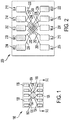
- FIG. 1 printed memory 100 includes a substrate 102, for example, a flexible dielectric substrate 102, such as a flexible polymer substrate, that may include an adhesive backing layer to aid in attachment of the printed memory 100 to a surface of a product, a plurality of wiring lines (e.g., WLs and BLs) 104 and a ferroelectric layer 106 directly interposed or positioned between the WLs and the BLs.
- a substrate 102 for example, a flexible dielectric substrate 102, such as a flexible polymer substrate, that may include an adhesive backing layer to aid in attachment of the printed memory 100 to a surface of a product, a plurality of wiring lines (e.g., WLs and BLs) 104 and a ferroelectric layer 106 directly interposed or positioned between the WLs and the BLs.
- a memory cell that stores the logic bit or logic state is provided by and within the ferroelectric layer 106 at the physical location that is interposed between the intersection of each WL and BL. It will thus be appreciated that the WLs and BLs do not physically contact each other, but are physically separated by the ferroelectric layer 106.
- the printed memory 100 depicted in FIG. 1 includes ten wiring lines 104 (five WLs and five BLs), and thus the FIG. 1 device includes 25 memory cells and may thus store 25 bits of information. Each wiring line 104 terminates in a contact pad 108. Each memory cell can be individually addressed through two of the contact pads (i.e., through one WL and one BL).
- the plurality of contact pads 108 may be arranged in a rectangular shape in two or more rows and columns as depicted, or they may be arranged in a single column. It will be appreciated that a XPM may include other structures that are not described or depicted for simplicity, while various depicted structures may be removed or modified.
- Each memory cell of the printed memory 100 may be read by applying a suitable read voltage to two of the wiring lines 104 (i.e., to one word line and one bit line) and measuring an electrical response. To apply the read voltage, the plurality of contact pads 108 can be physically and/or electrically contacted with probe contacts of a reader. A voltage is applied across the contact pads 108 through probe contacts, and the resulting response is measured.
- Each memory cell may be individually addressed during a read cycle or write cycle (hereinafter, a memory operation), and one or more of the memory cells in the memory array may be read or written simultaneously or serially.
- the contact pads 108 of the printed memory 100 and other electrical devices can be formed using a carbon-impregnated composite, electrically conductive inks such as silver nanoparticle ink, or one or more other suitable materials. These contact pads 108 can become scratched and degrade from repeated physical contact with, for example, electrical probes of a reader. Further, when direct physical contact is made between the reader and the printed memory 100, the reader must be correctly oriented with the printed memory 100.
- FIG. 2 is a schematic of memory 200, showing both WLs and BLs.
- BL contact pad BL0 202 includes BL 204
- BL contact pad BL1 includes 206 BL 208
- BL contact pad BL2 210 includes BL 212
- BL contact pad BL3 214 includes BL 216
- BL contact pad BL4 218 includes BL 220.
- WL contact pad WL0 222 includes WL 224
- WL contact pad WL1 226 includes WL 228,
- WL contact pad WL2 230 includes WL 232, WL contact pad WL3 includes 234 WL 236, and WL contact pad WL4 238 includes WL 240.
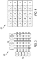
- FIG. 3 shows a simplified schematic of memory 300, where the numbers on electrode intersections denote the cell ID, according to examples of the present disclosure.
- FIG. 4 shows cell analog values 400 that are converted into binary values, where a cell becomes a '0' bit if its charge value is large, according to examples of the present disclosure.
- XPM is a 25-bit memory device which holds information in the form of states. These states are orientations of the polarization of the ferroelectric polymer located between two electrodes. A voltage is applied to create an electric field through the ferrous material. This allows the dipoles to align depending on the direction and magnitude of the field. Certain characteristics of the material, manufacturing process, size, and other physical features determine a minimum voltage required to "flip" the dipoles in the polymer.
- the S-curve is a graphical representation of polarization switching measured by the charge response of the polymer to the voltage applied vs the applied voltage. An ASIC is used to measure and store the charge response of the polymer. The S-curve shows how much voltage is needed to take the polymer from one "state” to another. Exploiting this switching dependence on applied bias can help further increase cell data storage.
- FIG. 5 shows an example S-curve 500 having these three main ranges depicted, according to examples of the present disclosure.
- Region 1 505 is a non-flipping region for a given pulse width. In this region the applied voltage is well below the required flipping voltage, but still significant enough to cause a response from a capacitive network.
- Region 2 510 is a non-linear or switching region. In this region, polarization starts to switch and may continue to switch depending on the applied bias across the cell.
- the non-linear region is divided into four encoding regimes that correspond to a first charge value less that 0.5nC, a second charge value between 0.5nC and 3nC, a third charge value between 3nC and 4.5nC, and a fourth value between 4.5nC and higher.
- Region 3 515 is a flipped or saturation region. In this region, all the cells are flipped into their new state where their polarization is now in line with the electric field from the applied bias. Any further increase in voltage will only increase the capacitive response of the cell; hence, the response or charge reading would increase slowly in contrast to region 2 510.
- Different ferroelectric polymers will have different onsets for the flipped region for a given ferroelectric layer thickness; hence, their starting point can be used as a means of differentiation.
- a first state could be ADC values less than 10.
- Another state in the "non-linear region can be defined for ADC counts from 10 to 70.
- a third state can be defined from 70 to 110 ADC counts.
- the final state would be the saturation region, or ADC values above 110.
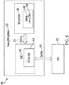
- FIG. 6 is a schematic depiction of an electronic system 600 for reading and/or writing to a XPM in accordance with an embodiment of the present teachings.
- the electronic system 600 comprises a microcontroller 604.
- the microcontroller 604 comprises a memory 606 that is configured to store a look-up table 608.
- the look-up table 608 stores an encoding/decoding scheme for converting one or more bits to write voltages and pulse widths or converting ADC values to bit values.
- the microcontroller 604 communicates with a ASIC 612 over a first data bus 610.
- the ASIC 612 comprises a A/D converter 614.
- the ASIC 612 executes read/write operations with the XPM 618 over a second data bus 616.
- FIG. 6 depicts an overview of one possible electronic system 600 design, it will be appreciated that other designs may include other features that are not depicted, while depicted features may be removed or modified. Moreover, the overview of FIG.6 is not intended to individually depict all supporting electronics such as microprocessors, memory, power supplies, etc., which may be designed into the present teachings by one of ordinary skill in the art.
- the first read operation includes the charge value associated with both polarization (P) and capacitive (C) effects (P+C) and the second read operation includes just the capacitive (C) effects.
- P polarization
- C capacitive
- P just the capacitive
- Raw ADC values read from memory below Table 2
- ADC1 ADC2 ADC1-ADC2 Decoded Bits LSB 25 18 7 11 21 21 0 11 27 25 2 11 25 27 -2 11 26 19 7 11 71 29 42 10 60 23 37 10 54 25 29 10 50 20 30 10 45 22 23 10 108 23 85 00 102 25 77 00 99 21 78 00 101 22 79 00 94 18 76 00 148 23 125 01 143 22 121 01 156 23 133 01 154 26 128 01 MSB 156 24 132 01
- LSB means least significant bit and MSB means most significant bit.
- the binary number is as follows: 0101-0101-0100-0000-0000-1010-1010-1011-1111-1111.
- the hexadecimal equivalent is 55400AABFF.
- each cell is written to once put the cell into a certain state representative of two bits of data.
- the states is one of four states comprising "11,” “01,” “10,” and "00.”
- a WL having five cells.
- a first portion of data that may be written on that WL to two cells is the "01" state.
- a second portion of data that may be written to the other three cells is the "00" state.
- each WL would step through the four states of "11,” “01,” “10,” and “00,” and apply a high impedance to the cells on that line which are not to be put in that state for that step.
- This can be illustrated as follows. For WL0: BL0, BL1 are “01,” BL2 is “10,” BL3 is “11,” and BL4 is “00.”
- An encoding scheme for the voltage and pulse width for "11” is sent to the ASIC, and everything but the BL3 is placed in high impedance, and the write is performed.
- an encoding scheme for "01” is sent to the ASIC, and BL2, BL3, BL4 are all placed in high impedance, then the write is performed.
- an encoding scheme for "10” is sent to the ASIC and everything but BL2 is placed in high impedance, and the write is performed.
- an encoding scheme for "00” is sent to the ASIC and everything but BL4 is placed in high impedance, and the write is performed.
- the data to be written can be segmented into a plurality of portions to be written in respective memory cells.
- Table 3 shows an example data segmentation.
- the first portion (10) of the entire data (0110... 00111010) is written to the first cell by a encoding scheme which would allow the cell to be put into the correct region for a charge reading which corresponds to "10”, then the second portion of the data is written to the second cell using the same process. This process continues until all the portions of the data are written to their corresponding cell.
- Each data portion value that is written is encoded using a specific pulse voltage and pulse width to achieve a distinctive polarization state of the ferroelectric cells.
- switching these polarization states induce four different charge values translating into four different ADC values that get decoded back into "00,” "01,” “10,” and “11” values.
- FIG. 7 shows a 3 ⁇ 3 XPM, according to examples of the present disclosure.
- Cell 0 is at the intersection of WL0 and BL0
- Cell 1 is at the intersection of WL0 and BL1
- Cell 2 is at the intersection of WL0 and BL2
- Cell 3 is at the intersection of WL1 and BL0
- Cell 4 is at the intersection of WL1 and BL1
- Cell 5 is at the intersection of WL1 and BL2
- Cell 6 is at the intersection of WL2 and BL0
- Cell 7 is at the intersection of WL2 and BL1
- Cell 8 is at the intersection of WL2 and BL2.
- FIG. 8 shows a computer-implemented method 800 for writing data to a printed memory device according to examples of the present disclosure.
- the computer-implemented method 800 begins by obtaining, at 802, first data by the microcontroller 604 to be written to the XPM. Referring to the example shown in Table 3, the first data to be written, (0110... 00111010), is obtained by the microcontroller 604.
- the computer-implemented method 800 continues by segmenting, at 804, the first data into n corresponding data portions by the microcontroller to be written to each cell of the XPM.
- the microcontroller 604 segments the data to be written into a plurality of data portions (e.g., 1 st portion ("10"), 2 nd portion ("10"), 3 rd portion ("11"), 4 th portion ("00"), ..., n -1th portion ("10"), nth portion ("01”)).
- the computer-implemented method 800 continues by determining, at 806, an encoding scheme (e.g., voltage and pulse width) for each of the nth data portions and identifying a cell of the XPM for which the data portions are to be written by the microcontroller.
- the computer-implemented method 800 continues by configuring, at 808, the ASIC a current encoding scheme by the microcontroller 604.
- the microcontroller 604 configures the ASIC 612 with an encoding scheme to encode each of the portions of data.
- the computer-implemented method 800 continues by selecting, at 810, target XPM cell(s) by selecting a corresponding WL and BL(s) associated to the n encoding scheme.
- the computer-implemented method 800 continues by setting, at 812, unaddressed WLs and BLs in high impedance by the ASIC 612.
- the computer-implemented method 800 continues by executing, at 814, a write operation by the ASIC 612.
- the computer-implemented method 800 continues by determining, at 816, whether all data portions of the first data have been written by the microcontroller 605.
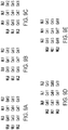
- FIG. 9B shows the next write operation where "00” is to be written to Cell 1 using a respective encoding scheme for "00” while BL0, BL2, WL1, and WL2 are placed in high impedance by the ASIC 612.
- FIG. 9C shows the next write operation where "00” is to be written to Cell 3 while BL1, BL2, WL0, and WL2 are placed in high impedance by the ASIC 612.
- FIG. 9D shows the next write operation where "11” is to be written to Cell 4 and Cell 5 using a respective encoding scheme for "11” while BL0, BL2, WL0, and WL2 are placed in high impedance by the ASIC 612.
- FIG. 9C shows the next write operation where "00” is to be written to Cell 3 while BL1, BL2, WL0, and WL2 are placed in high impedance by the ASIC 612.
- FIG. 9D shows the next write operation where "11” is to be written to Cell 4 and Cell 5 using a
- 9E shows the next write operation where "10” is to be written to Cell 6, Cell 7, and Cell 8 using a respective encoding scheme for "10" while WL0 and WL1 are placed in high impedance by the ASIC 612. If the determination at 816 is yes, then the computer-implemented method 800 concludes at 820.
- FIG. 10 shows a computer-implemented method 1000 for reading data from a printed memory device according to examples of the present disclosure.
- the computer-implemented method 1000 begins by sending, at 1002, a read encoding to the ASIC 612 by the microcontroller 602.
- the computer-implemented method 1000 continues by placing, at 1004, unselected WLs in high impedance.
- the computer-implemented method 1000 continues by placing, at 1006, unselected BLs in high impedance.
- the computer-implemented method 1000 continues by applying, at 1008, a stimulus to a selected cell that is to be read.
- the computer-implemented method 1000 continues by converting, at 1010, charge response to the ADC value via the ASIC 612.
- the computer-implemented method 1000 continues by storing, at 1012, cell ADC values in the ASIC 612.
- the computer-implemented method 1000 continues by determining, at 1014, whether both measurements have been taken. If the results of the determination at 1014 is no, then the method 1000 returns to 1008. If the result of the determination at 1014 is yes, then the method 1000 proceeds to 1016 where a determination is made as to whether all BLs are done. If the result of the determination at 1016 is no, then the method 1000 proceeds to 1018 where the next BL is selected. The method 1000 then proceeds from 1018 back to 1006. If the results of the determination at 1016 is yes, then the method 1000 proceeds to 1020 where a determination is made as to whether all WLs are done.
- the method 1000 proceeds to 1022 where the next WL is selected. The method 1000 then proceeds from 1022 back to 1004. If the results of the determination at 1020 is yes, then the method 1000 proceed to 1024 where every cell's ADC is sent to the microcontroller 602. The method 1000 continues by calculating, at 1026, a difference for each cell's two ADC values by the microcontroller 602. The method 1000 continues by converting, at 1028, via a look up table, the difference into data. The method 1000 continues by providing, 1030, the decoded values.
- the numerical values as stated for the parameter can take on negative values.
- the example value of range stated as "less than 10" can assume negative values, e.g. -1, -2, -3, -10, -20, -30, etc.
- one or more of the acts depicted herein may be carried out in one or more separate acts and/or phases.
- the terms “including,” “includes,” “having,” “has,” “with,” or variants thereof are used in either the detailed description and the claims, such terms are intended to be inclusive in a manner similar to the term “comprising.”
- the term “at least one of' is used to mean one or more of the listed items can be selected.
- the term “one or more of' with respect to a listing of items such as, for example, A and B means A alone, B alone, or A and B.
- the term “on” used with respect to two materials, one “on” the other, means at least some contact between the materials, while “over” means the materials are in proximity, but possibly with one or more additional intervening materials such that contact is possible but not required. Neither “on” nor “over” implies any directionality as used herein.
- the term “conformal” describes a coating material in which angles of the underlying material are preserved by the conformal material. The term “about” indicates that the value listed may be somewhat altered, as long as the alteration does not result in nonconformance of the process or structure to the illustrated implementation. Finally, "exemplary” indicates the description is used as an example, rather than implying that it is an ideal.
Landscapes
- Engineering & Computer Science (AREA)
- Computer Hardware Design (AREA)
- Theoretical Computer Science (AREA)
- Physics & Mathematics (AREA)
- Computer Security & Cryptography (AREA)
- Software Systems (AREA)
- General Engineering & Computer Science (AREA)
- General Physics & Mathematics (AREA)
- Microelectronics & Electronic Packaging (AREA)
- Mathematical Physics (AREA)
- Semiconductor Memories (AREA)
- Read Only Memory (AREA)
Applications Claiming Priority (1)
| Application Number | Priority Date | Filing Date | Title |
|---|---|---|---|
| US16/389,535 US10748597B1 (en) | 2019-04-19 | 2019-04-19 | Method and system for writing to and reading from a memory device |
Publications (2)
| Publication Number | Publication Date |
|---|---|
| EP3726531A2 true EP3726531A2 (de) | 2020-10-21 |
| EP3726531A3 EP3726531A3 (de) | 2021-02-17 |
Family
ID=70224234
Family Applications (1)
| Application Number | Title | Priority Date | Filing Date |
|---|---|---|---|
| EP20167847.1A Pending EP3726531A3 (de) | 2019-04-19 | 2020-04-02 | Verfahren und system zum schreiben in und lesen aus einer speichervorrichtung |
Country Status (5)
| Country | Link |
|---|---|
| US (2) | US10748597B1 (de) |
| EP (1) | EP3726531A3 (de) |
| JP (1) | JP7485532B2 (de) |
| KR (1) | KR102650244B1 (de) |
| CN (1) | CN111833951B (de) |
Families Citing this family (2)
| Publication number | Priority date | Publication date | Assignee | Title |
|---|---|---|---|---|
| US11939478B2 (en) | 2020-03-10 | 2024-03-26 | Xerox Corporation | Metallic inks composition for digital offset lithographic printing |
| US10979065B1 (en) * | 2020-04-01 | 2021-04-13 | Taiwan Semiconductor Manufacturing Company, Ltd. | Signal processing circuit, in-memory computing device and control method thereof |
Citations (4)
| Publication number | Priority date | Publication date | Assignee | Title |
|---|---|---|---|---|
| US3157857A (en) * | 1961-09-29 | 1964-11-17 | Indternat Business Machines Co | Printed memory circuit |
| WO2008031217A1 (en) * | 2006-09-13 | 2008-03-20 | Mosaid Technologies Incorporated | Flash multi-level threshold distribution scheme |
| US20160027790A1 (en) * | 2012-08-08 | 2016-01-28 | Chengdu Haicun Ip Technology Llc | Three-Dimensional Printed Memory |
| US9934415B1 (en) * | 2017-04-20 | 2018-04-03 | Xerox Corporation | Handheld reader having transparent circuit board for alignment of multiple electrical contacts |
Family Cites Families (16)
| Publication number | Priority date | Publication date | Assignee | Title |
|---|---|---|---|---|
| JP3875416B2 (ja) * | 1998-11-11 | 2007-01-31 | 富士通株式会社 | 強誘電体記憶装置 |
| US6856534B2 (en) | 2002-09-30 | 2005-02-15 | Texas Instruments Incorporated | Ferroelectric memory with wide operating voltage and multi-bit storage per cell |
| JP5005671B2 (ja) * | 2005-03-07 | 2012-08-22 | エヌエックスピー ビー ヴィ | 抵抗ヒステリシス素子を備えるメモリマトリックスの駆動 |
| US7619919B2 (en) | 2007-01-12 | 2009-11-17 | Marvell World Trade Ltd. | Multi-level memory |
| US7852671B2 (en) * | 2008-10-30 | 2010-12-14 | Micron Technology, Inc. | Data path for multi-level cell memory, methods for storing and methods for utilizing a memory array |
| JP5671335B2 (ja) | 2010-12-28 | 2015-02-18 | ラピスセミコンダクタ株式会社 | データ書き込み方法及び不揮発性半導体メモリ装置 |
| US8804425B2 (en) * | 2012-03-26 | 2014-08-12 | Sandisk Technologies Inc. | Selected word line dependent programming voltage |
| KR102056853B1 (ko) * | 2013-01-18 | 2020-01-22 | 삼성전자주식회사 | 저항성 메모리 장치 및 그에 따른 동작 제어방법 |
| US9886571B2 (en) | 2016-02-16 | 2018-02-06 | Xerox Corporation | Security enhancement of customer replaceable unit monitor (CRUM) |
| EP3286763A4 (de) * | 2016-03-31 | 2018-03-28 | Hewlett-Packard Enterprise Development LP | Identifizierung aussenliegender werte bei matrizen |
| US9899073B2 (en) * | 2016-06-27 | 2018-02-20 | Micron Technology, Inc. | Multi-level storage in ferroelectric memory |
| US10978169B2 (en) * | 2017-03-17 | 2021-04-13 | Xerox Corporation | Pad detection through pattern analysis |
| US10153022B1 (en) * | 2017-06-09 | 2018-12-11 | Micron Technology, Inc | Time-based access of a memory cell |
| US10304514B2 (en) * | 2017-07-05 | 2019-05-28 | Micron Technology, Inc. | Self-reference sensing for memory cells |
| US10446198B2 (en) * | 2017-10-02 | 2019-10-15 | Micron Technology, Inc. | Multiple concurrent modulation schemes in a memory system |
| US10608642B2 (en) * | 2018-02-01 | 2020-03-31 | iCometrue Company Ltd. | Logic drive using standard commodity programmable logic IC chips comprising non-volatile radom access memory cells |
-
2019
- 2019-04-19 US US16/389,535 patent/US10748597B1/en active Active
-
2020
- 2020-03-20 CN CN202010204979.XA patent/CN111833951B/zh active Active
- 2020-03-30 JP JP2020059741A patent/JP7485532B2/ja active Active
- 2020-04-01 KR KR1020200040015A patent/KR102650244B1/ko active Active
- 2020-04-02 EP EP20167847.1A patent/EP3726531A3/de active Pending
- 2020-05-22 US US16/881,745 patent/US10878875B2/en active Active
Patent Citations (4)
| Publication number | Priority date | Publication date | Assignee | Title |
|---|---|---|---|---|
| US3157857A (en) * | 1961-09-29 | 1964-11-17 | Indternat Business Machines Co | Printed memory circuit |
| WO2008031217A1 (en) * | 2006-09-13 | 2008-03-20 | Mosaid Technologies Incorporated | Flash multi-level threshold distribution scheme |
| US20160027790A1 (en) * | 2012-08-08 | 2016-01-28 | Chengdu Haicun Ip Technology Llc | Three-Dimensional Printed Memory |
| US9934415B1 (en) * | 2017-04-20 | 2018-04-03 | Xerox Corporation | Handheld reader having transparent circuit board for alignment of multiple electrical contacts |
Non-Patent Citations (1)
| Title |
|---|
| CHANG SHOUDE ET AL: "Printed Flexible FE Memory Array Testing System", 2018 7TH ELECTRONIC SYSTEM-INTEGRATION TECHNOLOGY CONFERENCE (ESTC), IEEE, 18 September 2018 (2018-09-18), pages 1 - 3, XP033452854, DOI: 10.1109/ESTC.2018.8546339 * |
Also Published As
| Publication number | Publication date |
|---|---|
| US10748597B1 (en) | 2020-08-18 |
| EP3726531A3 (de) | 2021-02-17 |
| JP2020177721A (ja) | 2020-10-29 |
| US10878875B2 (en) | 2020-12-29 |
| US20200335149A1 (en) | 2020-10-22 |
| CN111833951A (zh) | 2020-10-27 |
| KR102650244B1 (ko) | 2024-03-25 |
| KR20200123003A (ko) | 2020-10-28 |
| JP7485532B2 (ja) | 2024-05-16 |
| CN111833951B (zh) | 2022-11-29 |
Similar Documents
| Publication | Publication Date | Title |
|---|---|---|
| KR101622817B1 (ko) | 저항 메모리 센싱 방법 및 디바이스 | |
| US20190006020A1 (en) | Word line leakage detection with common mode tracking | |
| US7764529B2 (en) | Data storage device | |
| WO2007008701A3 (en) | Apparatus and method for programming an array of nonvolatile memory cells including switchable resistor memory elements | |
| US9401216B1 (en) | Adaptive operation of 3D NAND memory | |
| TW200710678A (en) | Apparatus and method for reading an array of nonvolatile memory cells including switchable resistor memory elements | |
| EP3726531A2 (de) | Verfahren und system zum schreiben in und lesen aus einer speichervorrichtung | |
| US9007824B2 (en) | Boosting memory reads | |
| EP3641511A1 (de) | Ausrichtungsagnostisches verfahren zur schnittstelle zu einem xeroxdruckspeicheretikett | |
| CN115083452B (zh) | 存储器件 | |
| EP1492123A2 (de) | Magnetischer Speicher | |
| US10867654B2 (en) | Method for testing a memory device | |
| US20090086613A1 (en) | Non-Destructive Readback For Ferroelectric Material | |
| US12073864B2 (en) | Memory cell sensing using two step word line enabling | |
| JP4483540B2 (ja) | 記憶装置 | |
| KR102818319B1 (ko) | 메모리 감지를 위한 평균 기준 전압 | |
| JP2020013989A (ja) | 改善された歩留まりを示す印刷された電子デバイス | |
| JP4182671B2 (ja) | 強誘電体記憶装置の調整方法 | |
| JP2004303333A (ja) | 強誘電体記憶装置及びその選択電圧調整方法 |
Legal Events
| Date | Code | Title | Description |
|---|---|---|---|
| PUAI | Public reference made under article 153(3) epc to a published international application that has entered the european phase |
Free format text: ORIGINAL CODE: 0009012 |
|
| STAA | Information on the status of an ep patent application or granted ep patent |
Free format text: STATUS: THE APPLICATION HAS BEEN PUBLISHED |
|
| AK | Designated contracting states |
Kind code of ref document: A2 Designated state(s): AL AT BE BG CH CY CZ DE DK EE ES FI FR GB GR HR HU IE IS IT LI LT LU LV MC MK MT NL NO PL PT RO RS SE SI SK SM TR |
|
| AX | Request for extension of the european patent |
Extension state: BA ME |
|
| PUAL | Search report despatched |
Free format text: ORIGINAL CODE: 0009013 |
|
| AK | Designated contracting states |
Kind code of ref document: A3 Designated state(s): AL AT BE BG CH CY CZ DE DK EE ES FI FR GB GR HR HU IE IS IT LI LT LU LV MC MK MT NL NO PL PT RO RS SE SI SK SM TR |
|
| AX | Request for extension of the european patent |
Extension state: BA ME |
|
| RIC1 | Information provided on ipc code assigned before grant |
Ipc: G11C 11/56 20060101ALI20210114BHEP Ipc: G11C 11/22 20060101AFI20210114BHEP |
|
| STAA | Information on the status of an ep patent application or granted ep patent |
Free format text: STATUS: REQUEST FOR EXAMINATION WAS MADE |
|
| 17P | Request for examination filed |
Effective date: 20210817 |
|
| RBV | Designated contracting states (corrected) |
Designated state(s): AL AT BE BG CH CY CZ DE DK EE ES FI FR GB GR HR HU IE IS IT LI LT LU LV MC MK MT NL NO PL PT RO RS SE SI SK SM TR |
|
| STAA | Information on the status of an ep patent application or granted ep patent |
Free format text: STATUS: EXAMINATION IS IN PROGRESS |
|
| 17Q | First examination report despatched |
Effective date: 20220202 |