EP3723478B1 - Verfahren und vorrichtung zur anwendung, überwachung und anpassung eines reizes auf ein haustier - Google Patents
Verfahren und vorrichtung zur anwendung, überwachung und anpassung eines reizes auf ein haustier Download PDFInfo
- Publication number
- EP3723478B1 EP3723478B1 EP18887374.9A EP18887374A EP3723478B1 EP 3723478 B1 EP3723478 B1 EP 3723478B1 EP 18887374 A EP18887374 A EP 18887374A EP 3723478 B1 EP3723478 B1 EP 3723478B1
- Authority
- EP
- European Patent Office
- Prior art keywords
- voltage
- time
- microcontroller
- secondary circuit
- intensity level
- Prior art date
- Legal status (The legal status is an assumption and is not a legal conclusion. Google has not performed a legal analysis and makes no representation as to the accuracy of the status listed.)
- Active
Links
Images






Classifications
-
- A—HUMAN NECESSITIES
- A01—AGRICULTURE; FORESTRY; ANIMAL HUSBANDRY; HUNTING; TRAPPING; FISHING
- A01K—ANIMAL HUSBANDRY; AVICULTURE; APICULTURE; PISCICULTURE; FISHING; REARING OR BREEDING ANIMALS, NOT OTHERWISE PROVIDED FOR; NEW BREEDS OF ANIMALS
- A01K15/00—Devices for taming animals, e.g. nose-rings or hobbles; Devices for overturning animals in general; Training or exercising equipment; Covering boxes
- A01K15/02—Training or exercising equipment, e.g. mazes or labyrinths for animals ; Electric shock devices; Toys specially adapted for animals
- A01K15/021—Electronic training devices specially adapted for dogs or cats
- A01K15/022—Anti-barking devices
-
- H—ELECTRICITY
- H05—ELECTRIC TECHNIQUES NOT OTHERWISE PROVIDED FOR
- H05C—ELECTRIC CIRCUITS OR APPARATUS SPECIALLY DESIGNED FOR USE IN EQUIPMENT FOR KILLING, STUNNING, OR GUIDING LIVING BEINGS
- H05C1/00—Circuits or apparatus for generating electric shock effects
- H05C1/04—Circuits or apparatus for generating electric shock effects providing pulse voltages
Definitions
- the disclosure herein involves dynamic voltage modulation.
- Pet training and containment is essential for pet owners.
- One of the most common humane and effective training methods is electrical stimulation of the pet animal. Short electrical pulses are used to communicate desired behaviors.
- US 2008/0216766 describes a remote receiving circuit for providing and controlling an electric stimulus applied to an animal including an electronic switch powered by a battery in series on a primary of a high-voltage transformer and whose on/off state can be modified by control pulses to create a source of alternating current to supply the primary of the transformer.
- the circuit further includes a first electrode and a second electrode configured to be in contact with the animal and connected to the respective ends of a secondary of the transformer, and a device for measuring the peak intensity of a stimulus current applied by the electrodes to the animal's body.
- the present invention provides a device as set out in claim 1, and a method to be performed on the device, as set out in claim 4. Further embodiments are defined in the in dependent claims.
- Systems and methods are herein proposed in this application that precisely deliver electrical pulses to the pet through electrodes and that are able to determine delivery effectiveness of these pulses in a measureable manner. Based on the measured delivery effectiveness of pulses, subsequent pulses may be adjusted to increase the chances of delivery effectiveness if it is determined that successful delivery has not yet occurred. Subsequent pulses may be adjusted to minimize pulse magnitudes to decrease stress to the pet while still maintaining effectiveness if it is determined that successful delivery has occurred.
- An electrical stimulus pulse development of an embodiment uses a method to precisely control the voltage and timing of energy pulses that are delivered to the pet.
- Load resistance may be accurately determined under an embodiment.
- Load resistance is an indicator of skin conduction, which is an indicator of pulse delivery effectiveness. Identifying the point in time when skin breakdown occurs allows for a reduction in voltage level on subsequent pulses while still eliciting a similar response. Identifying the fact that the skin is not breaking down due to stimulus pulses indicates a need to increase the voltage to maximize the chance of breakdown and conduction.
- the use of this new technology allows for a much smaller design.
- the size can be much smaller than with typical techniques as it is not required to deliver a charge from a single cycle of its magnetic potential. It may take several hundred, or even several thousand cycles of charge from the transformer to build up energy in the storage components before the energy is released.
- the fact that the system requires an extended period of time to restore the depleted energy means there is time to monitor and control the precise voltage and also determine effectiveness of the prior pulse due to the amount of energy required to refill the storage components.
- the systems and methods described herein include a method used to develop, apply (release), analyze, and adjust electrical stimulus pulses based on the load conditions of the pet skin.
- the electrical stimulus approach utilizes a microprocessor to control all aspects of stimulus development, release, and monitoring.
- the microprocessor controls a switched mode power supply, consisting of transformer and voltage doubler(s) to step-up the input voltage.
- the voltage is presented to storage component(s) (typically capacitors) for storage which is exposed on an electrode. This stored charge is monitored by the processor via a feedback loop.
- a high voltage switch i.e., transistor
- the processor determines a threshold voltage level is reached and any additional desired delay time is added, a high voltage switch (i.e., transistor) is switched on by the processor for the desired stimulus pulse length to complete a return path on a second electrode providing a path for current to flow from one electrode, through the pet's skin, into the second electrode, and to system return.
- the feedback loop allows for real time monitoring of voltage level and charge time. This knowledge allows a processing unit to: (i) precisely and accurately determine the stimulus pulse magnitude and (ii) monitor the recharge time.
- the feedback loop therefore allows determination of the depleted charge using recharge time as a direct indicator of load resistance (skin resistance). Based on depleted charge findings, subsequent pulses may be:
- Figure 1 shows a circuit 100 for monitoring stimulus levels in controlling delivery of precise electrical stimulation to an animal.
- Figure 1 shows a microcontroller 102 which controls a DC-DC converter (i.e. transformer plus voltage multiplier) 104 which steps up the input voltage. The stepped-up voltage is then presented to a storage component (typically capacitor(s)) 106 for storage.
- the storage component may include one or more capacitors which are connected to a first (high voltage) electrode 110.
- the circuit shown in Figure 1 shows a feedback connection 108 between the first electrode and the microcontroller 102 such that the microcontroller may monitor potential energy at the first electrode.
- the microcontroller also controls a return switch 114.
- the microcontroller may then use the return switch 114 to provide a return path to voltage stored in the storage component after passing through the pet skin.
- the switch may comprise a transistor and may provide the return path for the desired stimulus pulse length. Stimulus delivery then comprises current flow from the first electrode 110 through the pet's skin (i.e. resistive load 140), into the second return electrode 112, and to system return (ground).
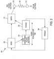
- Figure 2 shows the same components of the circuit described above. However, the circuit 200 of Figure 2 places the transistor switch 214 directly between the microcontroller 202 and the first electrode 210.
- the DC-DC converter 204 steps up voltage delivered by the microcontroller and charges the storage 206 component.
- a feedback connection 208 is provided between the storage component 206 and the microcontroller 202.
- the microcontroller 202 controls a transistor 214 in providing a pathway between the storage component 206 (charged by the DC-DC converter 204) and the first electrode 210 for a desired stimulus pulse length.
- current flows from the storage component to the first electrode 210 through the pet's skin (or resistive load 240), into the second return electrode 212, and to system return (ground).
- the return electrode 212 in contact with the animal skin, is always connected to system return (ground).
- Figure 3 shows a circuit 300 for developing, applying and monitoring stimulus levels in controlling delivery of electrical stimulation to an animal, under an embodiment.
- Figure 3 shows voltage regulator 310 and microprocessor 320.
- Figure 3 shows the transformer-primary control 330.
- the Field-Effect Transistor (FET) 340 acts as a switch at a frequency and duty cycle to efficiently allow current to flow through the primary of the step-up transformer 350.
- Element 360 of Figure 3 demonstrates two stages of voltage doublers, which creates a voltage quadrupler, under an embodiment. As many stages as required may be cascaded for the specific application (in combination with the turns ratio of the step-up transformer). Accordingly, the step-up transformer 350 and voltage quadrupler 360 component comprise a DC-DC Step-up converter.
- Voltage divider 370 reduces the high voltage output to a level compatible with the microprocessor inputs.
- Figure 3 shows a controllable high voltage return path 380. This return path controls the duration of the stimulation pulse by providing a path from the high voltage electrode, through the skin, into the low side electrode, and to system ground.
- FIG. 4 shows a method for modulating stimulus delivery to an animal.
- a first step 402 involves applying a stimulus command, i.e. a command to deliver an electrical stimulus using the feedback control circuit described herein.
- Step 404 comprises setting a voltage threshold to an initial value.
- Step 406 involves a microcontroller controlling a DC-DC converter to provide a voltage to a storage component to drive and build voltage potential.
- the method iteratively checks the voltage 408 to determine if a threshold is met. If no 410 then voltage development and storage continues. If yes 412, the method proceeds to step 414 to determine if an additional delay is expired. If not 418 then the method maintains voltage at the stored potential level.
- the microcontroller enables the return switch for a time specified or determined by a given stimulus level 421, i.e. the stimulus is applied to the animal.
- the microcontroller then disables the switch 422, i.e. return pathway. If application of the stimulus command is discontinued 424, then the method of stimulus delivery is also discontinued.
- the method starts a timer 426.
- the microcontroller controls a DC-DC converter to provide a voltage to a storage component to drive and build voltage potential 427.
- Step 428 determines whether the stored voltage achieves a set threshold (which may be a fraction of the originally established threshold at step 408). If not 432, charging continues. Once this threshold voltage is realized 434, the method stops the timer 436. Measured time values provide information of skin breakdown. If the measured time value is greater than a value indicating breakdown 437, then low resistance is detected 438. In this event, the voltage threshold is set to a lower value considering that skin resistance is low 440.
- the method passes through steps 437 and 442 as a "no" then the method at step 448 may either maintain or incrementally increase the voltage threshold based on the timer value, under an embodiment. The method at step 448 may also incrementally decrease the voltage threshold based on the timer value, under an embodiment. After any of the three voltage threshold assessment events, the method returns to step 408 of the stimulus command workflow process.
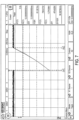
- the oscilloscope trace of Figure 5 shows the high voltage electrode and return electrode during the period where the return path switch is activated.
- this switch is activated for a period of time about 85 microseconds.
- the ground electrode attains a voltage equivalent to ground almost immediately.
- the high voltage electrode starts at the full storage component voltage level and decreases as energy is depleted.
- This voltage drop is an indicator of the energy drawn from the system's storage. The lower the pet skin resistance, the more energy is being depleted from the system. The lower the pet skin resistance, the more energy that is being delivered to the pet.
- oscilloscope traces seen in Figures 6-9 show the high voltage electrode and return electrode before stimulus delivery, during stimulus delivery, and when restoring the energy depleted during the stimulus delivery.
- the start of the gap in the traces indicates the instant a short (i.e., 1 microsecond to 200 microsecond) pulse is activated by turning on the "return switch" to enable a return path from the return electrode to ground. This period is where current is allowed to flow from the high voltage electrode, through the skin of the pet, and then to system return (ground). Following this brief period, the remainder of the gap is the period of time required to recharge the storage component(s). This period of time indicates the energy drawn from the system's storage.
- Figure 6 shows a single electrical pulse followed by energy recovery assuming a 500 ohm skin resistance. A 500 ohm load indicates strong dermal contact. Figure 6 shows an 18.5ms recovery time (X1 to X2).
- Figure 7 shows a single electrical pulse followed by energy recovery assuming a 10K ohm skin resistance. A 10K ohm load indicates weak dermal contact. Figure 7 shows a 12.3 ms recovery (X1 to X2).
- Figure 8 shows a single electrical pulse followed by energy recovery assuming minimal to no skin resistance, i.e. weak dermal contact. The very high resistive load indicates minimal to no dermal contact. Figure 8 shows an immediate recovery, indicating no energy was drained from the system during the stimulation.
- Increased energy depletion indicates that skin resistance has decreased. Therefore, voltage can be decreased while still applying a sufficient stimulus.
- Figure 9 shows a scope trace that illustrates this particular action.
- the first pulse of each pulse train is applied at a high voltage level.
- the system determines, based on skin resistance, that skin breakdown has occurred. Therefore, the subsequent pulses are applied at a lower voltage level while still delivering an adequate energy level.
- the efficacy of each pulse is monitored. If any pulse is determined to be ineffective, the developed voltage can be returned to a high enough level to cause breakdown.
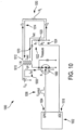
- Figure 10 shows a microcontroller 1002 driving current/voltage to circuit 1000.
- the circuit delivers an electrical stimulus to an animal wearing a collar housing the circuit.
- the circuit delivers the stimulus at resistor 1050 ( R L ) which models the resistive load presented to the circuit (i.e., R L is a model for the skin of the animal wearing the collar).
- a method of measuring the intensity of the stimulus delivered at resistor 1050 ( R L ) is described herein.
- the method includes setting the general purpose input/output (GPIO) 1004 pin to high.
- a one shot timer with interrupt on time out is configured to maintain the high position for the desired pulse width.
- the one shot timer works something like an alarm clock.
- the microcontroller 1002 provides a control voltage 1006 ( V control ) which allows primary current 1008 ( I pri ) to flow.
- the transistor 1060 functions as a switch, i.e. the transistor allows primary current 1008 ( I pri ) to flow when control voltage 1006 ( V control ) is applied).
- the primary current 1008 ( I pri ) flows through primary winding 1010 ( L pri ).
- the transformer comprises primary to secondary winding ratio of 1:N. Secondary current will be induced to flow as a result of a flyback phase reversal when the primary current is stopped by the removal of the control signal at transistor 1060.
- the secondary current 1014 ( I sec ) provides a voltage drop across resistor 1050 ( R L ), i.e. power dissipation at R L or delivery of stimulus to the animal.
- the microcontroller 1002 In the timer interrupt service routine, the microcontroller 1002 returns the GPIO 1004 to low. Immediately following this instruction, the microcontroller 1002 triggers the analog to digital converter 1018 to sample voltage ( V measure ) at location 1020 between resistor 1022 ( R 1 ) and resistor 1024 ( R 2 ).
- the microcontroller sets GPIO 1004 to high.
- Figure 11A shows a one shot timer with interrupt for desired pulse width t 1 .
- the microcontroller shuts the GPIO 1004 off, i.e. returns it to low, at time t 1 .
- the microcontroller then triggers the ADC to sample voltage ( V measure ) of the circuit at location 1020 at t 1 . It will take a small amount of time for the microcontroller and its ADC to initiate and complete the conversion, therefore the ADC sample ( V measure ) occurs at a time t 2 which is slightly greater than t 1 .
- Figure 11B shows primary current ( I pri ) as a function of time during the configured one shot pulse width.
- Figure 11C shows secondary current ( I sec ) as a function of time after time t 1 , i.e. after the microcontroller returns GPIO 1004 to low.
- Figure 11D shows sample voltage V measure over time.
- the decay characteristics of V measure (t) correspond to the decay characteristics of I sec as shown in Figure 11C .
- microcontroller 1002 reads and saves an ADC measurement of voltage at location 1020 and at time t 2 (described previously), i.e. the ADC measures V measure ( t 2 ) .
- a one-shot timer is configured with interrupt on timeout for desired width t 3 - t 2 .
- the microcontroller 1002 reads and saves an ADC measurement of voltage at location 1020 and at time t 3 , i.e. the ADC measures V measure ( t 3 ) .
- V measure ( t 2 ) , V measure ( t 3 ) , t 2 , t 3 , R 2 , and Tc to compute intensity of electrical stimulus delivered by circuit 1000.
- V measure t 2 V measure t 3 R 2 ⁇ I sec ⁇ pk ⁇ e ⁇ t 2 ⁇ t 1 / Tc R 2 ⁇ I sec ⁇ pk ⁇ e ⁇ t 3 ⁇ t 1 / Tc
- V measure t 2 V measure t 3 e ⁇ t 2 ⁇ t 1 /Tc e ⁇ t 3 ⁇ t 1 / Tc
- V measure t 2 V measure t 3 e ⁇ t 2 ⁇ t 1 / Tc + t 3 ⁇ t 1 / Tc
- V measure t 2 V measure t 3 ⁇ t 2 ⁇ t 1 / Tc + t 3 ⁇ t 1 / Tc
- V measure t 2 V measure t 3
- equations (6) and (9) are based on voltage measurements ( V measure ( t 2 ) , V measure ( t 3 )) , known time values ( t 2 , t 3 ), known resistor value R 2 , and known (deduced) time constant value Tc.
- a feedback control loop may now be employed to provide a nearly constant INTENSITY for variations in Tc. Hence, the device may compensate for changes in R L .
- a device comprises under one embodiment a microcontroller coupled to a transformer, wherein the transformer comprises a primary winding and a secondary winding, wherein the microcontroller is connected to a secondary circuit at a first location.
- the microcontroller is configured to provide a voltage at a first value to the primary winding for a first period of time, the providing the voltage for the first period of time including initiating delivery of the voltage at time t 0 and ceasing the delivery at time t 1 , the ceasing the delivery inducing a flow of current through the secondary winding and the secondary circuit, wherein the secondary circuit comprises at least one resistor, at least one diode, and a resistive load, wherein the resistive load is variable.
- the microcontroller is configured to measure a first voltage at the first location in the secondary circuit at time t 2 and to measure a second voltage at the first location at time t 3 .
- the microcontroller is configured to compute a time constant of the secondary circuit using a difference between time t 3 and time t 2 , the first measured voltage, and the second measured voltage.
- the microcontroller is configured to compute a peak current in the secondary circuit using a value of the at least one resistor and the first measured voltage.
- the microcontroller configured to compute an intensity level at the resistive load using the computed peak current and the time constant of the secondary circuit.
- the microcontroller is configured to monitor the intensity level, the monitoring the intensity level including iteratively performing the providing a voltage at the first value to the primary winding for the first period of time, the measuring the first voltage and the second voltage, the computing the time constant, the computing the peak current, and the computing the intensity level.
- the monitoring the intensity level of an embodiment includes maintaining the intensity level at a near constant value by iteratively adjusting at least one of the first value and the first period of time.
- Computer networks suitable for use with the embodiments described herein include local area networks (LAN), wide area networks (WAN), Internet, or other connection services and network variations such as the world wide web, the public internet, a private internet, a private computer network, a public network, a mobile network, a cellular network, a value-added network, and the like.
- Computing devices coupled or connected to the network may be any microprocessor controlled device that permits access to the network, including terminal devices, such as personal computers, workstations, servers, mini computers, main-frame computers, laptop computers, mobile computers, palm top computers, hand held computers, mobile phones, TV set-top boxes, or combinations thereof.
- the computer network may include one of more LANs, WANs, Internets, and computers.
- the computers may serve as servers, clients, or a combination thereof.
- the systems and methods for dynamic voltage modulation can be a component of a single system, multiple systems, and/or geographically separate systems.
- the systems and methods for dynamic voltage modulation can also be a subcomponent or subsystem of a single system, multiple systems, and/or geographically separate systems.
- the components of systems and methods for dynamic voltage modulation can be coupled to one or more other components (not shown) of a host system or a system coupled to the host system.
- One or more components of the systems and methods for dynamic voltage modulation and/or a corresponding interface, system or application to which the systems and methods for dynamic voltage modulation is coupled or connected includes and/or runs under and/or in association with a processing system.
- the processing system includes any collection of processor-based devices or computing devices operating together, or components of processing systems or devices, as is known in the art.
- the processing system can include one or more of a portable computer, portable communication device operating in a communication network, and/or a network server.
- the portable computer can be any of a number and/or combination of devices selected from among personal computers, personal digital assistants, portable computing devices, and portable communication devices, but is not so limited.
- the processing system can include components within a larger computer system.
- the processing system of an embodiment includes at least one processor and at least one memory device or subsystem.
- the processing system can also include or be coupled to at least one database.
- the term "processor” as generally used herein refers to any logic processing unit, such as one or more central processing units (CPUs), digital signal processors (DSPs), application-specific integrated circuits (ASIC), etc.
- the processor and memory can be monolithically integrated onto a single chip, distributed among a number of chips or components, and/or provided by some combination of algorithms.
- the methods described herein can be implemented in one or more of software algorithm(s), programs, firmware, hardware, components, circuitry, in any combination.
- Communication paths couple the components and include any medium for communicating or transferring files among the components.
- the communication paths include wireless connections, wired connections, and hybrid wireless/wired connections.
- the communication paths also include couplings or connections to networks including local area networks (LANs), metropolitan area networks (MANs), wide area networks (WANs), proprietary networks, interoffice or backend networks, and the Internet.
- LANs local area networks
- MANs metropolitan area networks
- WANs wide area networks
- proprietary networks interoffice or backend networks
- the Internet and the Internet.
- the communication paths include removable fixed mediums like floppy disks, hard disk drives, and CD-ROM disks, as well as flash RAM, Universal Serial Bus (USB) connections, RS-232 connections, telephone lines, buses, and electronic mail messages.
- USB Universal Serial Bus
- aspects of the systems and methods for dynamic voltage modulation and corresponding systems and methods described herein may be implemented as functionality programmed into any of a variety of circuitry, including programmable logic devices (PLDs), such as field programmable gate arrays (FPGAs), programmable array logic (PAL) devices, electrically programmable logic and memory devices and standard cell-based devices, as well as application specific integrated circuits (ASICs).
- PLDs programmable logic devices
- FPGAs field programmable gate arrays
- PAL programmable array logic
- ASICs application specific integrated circuits
- microcontrollers with memory such as electronically erasable programmable read only memory (EEPROM)
- embedded microprocessors firmware, software, etc.
- aspects of the systems and methods for dynamic voltage modulation and corresponding systems and methods may be embodied in microprocessors having software-based circuit emulation, discrete logic (sequential and combinatorial), custom devices, fuzzy (neural) logic, quantum devices, and hybrids of any of the above device types.
- the underlying device technologies may be provided in a variety of component types, e.g., metal-oxide semiconductor field-effect transistor (MOSFET) technologies like complementary metal-oxide semiconductor (CMOS), bipolar technologies like emitter-coupled logic (ECL), polymer technologies (e.g., silicon-conjugated polymer and metal-conjugated polymer-metal structures), mixed analog and digital, etc.
- MOSFET metal-oxide semiconductor field-effect transistor
- CMOS complementary metal-oxide semiconductor
- bipolar technologies like emitter-coupled logic (ECL)
- polymer technologies e.g., silicon-conjugated polymer and metal-conjugated polymer-metal structures
- any system, method, and/or other components disclosed herein may be described using computer aided design tools and expressed (or represented), as data and/or instructions embodied in various computer-readable media, in terms of their behavioral, register transfer, logic component, transistor, layout geometries, and/or other characteristics.
- Computer-readable media in which such formatted data and/or instructions may be embodied include, but are not limited to, non-volatile storage media in various forms (e.g., optical, magnetic or semiconductor storage media) and carrier waves that may be used to transfer such formatted data and/or instructions through wireless, optical, or wired signaling media or any combination thereof.
- Examples of transfers of such formatted data and/or instructions by carrier waves include, but are not limited to, transfers (uploads, downloads, e-mail, etc.) over the Internet and/or other computer networks via one or more data transfer protocols (e.g., HTTP, FTP, SMTP, etc.).
- data transfer protocols e.g., HTTP, FTP, SMTP, etc.
- a processing entity e.g., one or more processors
- processors within the computer system in conjunction with execution of one or more other computer programs.
Landscapes
- Life Sciences & Earth Sciences (AREA)
- Environmental Sciences (AREA)
- General Health & Medical Sciences (AREA)
- Health & Medical Sciences (AREA)
- Physical Education & Sports Medicine (AREA)
- Animal Behavior & Ethology (AREA)
- Zoology (AREA)
- Animal Husbandry (AREA)
- Biodiversity & Conservation Biology (AREA)
- Insects & Arthropods (AREA)
- Electrotherapy Devices (AREA)
- Charge And Discharge Circuits For Batteries Or The Like (AREA)
- Measurement Of Current Or Voltage (AREA)
Claims (5)
- Vorrichtung (1000), umfassend:eine Mikrosteuerung (1002), die mit einem Transformator gekoppelt ist, wobei der Transformator eine Primärwicklung (1010) und eine Sekundärwicklung (1012) umfasst, wobei die Mikrosteuerung mit einem Sekundärstromkreis an einer ersten Stelle verbunden ist;wobei:die Mikrosteuerung dazu ausgelegt ist, über eine erste Zeitspanne hinweg eine Spannung (1006, Vcontrol) mit einem ersten Wert für die Primärwicklung bereitzustellen, wobei das Bereitstellen der Spannung über die erste Zeitspanne hinweg das Initiieren der Zufuhr der Spannung zu einer Zeit to und das Beenden der Zufuhr zu einer Zeit t1 umfasst, wobei das Beenden der Zufuhr einen Stromfluss (Isec) durch die Sekundärwicklung und den Sekundärstromkreis induziert, wobei der Sekundärstromkreis zumindest einen Widerstand (1022, 1024), zumindest eine Diode (1070) und eine Widerstandslast (1050, RL) umfasst, wobei die Widerstandslast variabel ist;die Mikrosteuerung dazu ausgelegt ist, zu einer Zeit t2 eine erste Spannung an der ersten Stelle im Sekundärstromkreis zu messen und zu einer Zeit t3 eine zweite Spannung an der ersten Stelle zu messen;die Mikrosteuerung dazu ausgelegt ist, einen Spitzenstrom an der ersten Stelle in dem Sekundärstromkreis unter Verwendung eines Werts des zumindest einen Widerstands und der ersten gemessenen Spannung zu berechnen;dadurch gekennzeichnet, dass:die Mikrosteuerung dazu ausgelegt ist, eine Zeitkonstante des Sekundärstromkreises unter Verwendung einer Differenz zwischen der Zeit t3 und der Zeit t2, der ersten gemessenen Spannung und der zweiten gemessenen Spannung zu berechnen; unddie Mikrosteuerung dazu ausgelegt ist, einen Intensitätspegel an der Widerstandslast unter Verwendung des berechneten Spitzenstroms und der Zeitkonstante des Sekundärstromkreises zu berechnen; unddie Mikrosteuerung dazu ausgelegt ist, den Intensitätspegel zu überwachen, wobei das Überwachen des Intensitätspegels das iterative Durchführen des Bereitstellens einer Spannung mit dem ersten Wert für die Primärwicklung über die erste Zeitspanne hinweg, das Messen der ersten Spannung und der zweiten Spannung, das Berechnen der Zeitkonstante, das Berechnen des Spitzenstroms und das Berechnen des Intensitätspegels umfasst.
- Vorrichtung nach Anspruch 1, wobei das Überwachen des Intensitätspegels das Aufrechterhalten des Intensitätspegels auf einem nahezu konstanten Wert durch iteratives Anpassen von zumindest einem aus dem ersten Wert und der ersten Zeitspanne umfasst.
- Vorrichtung nach Anspruch 1 oder 2, wobei die Vorrichtung dazu ausgelegt ist, einen elektrischen Stimulus an die Haut eines Tiers anzulegen, wobei die Haut des Tiers die Widerstandslast ist.
- Verfahren, das mit einer Vorrichtung nach einem der Ansprüche 1 bis 3 durchgeführt wird, wobei das Verfahren Folgendes umfasst:Bereitstellen der Spannung mit dem ersten Wert für die Primärwicklung des Transformators über die erste Zeitspanne hinweg, wobei das Bereitstellen der Spannung über die erste Zeitspanne hinweg das Initiieren der Zufuhr der Spannung zu einer Zeit to und das Beenden der Zufuhr zu einer Zeit t1 umfasst, wobei das Beenden der Zufuhr einen Stromfluss durch eine Sekundärwicklung des Transformators und den Sekundärschaltkreis induziert;Messen der ersten Spannung an einer ersten Stelle in dem Sekundärstromkreis zu einer Zeit t2 und Messen der zweiten Spannung an der ersten Stelle im Sekundärstromkreis zu einer Zeit t3;Berechnen der Zeitkonstante des Sekundärstromkreises unter Verwendung der Differenz zwischen den Zeiten t3 und t2, der ersten gemessenen Spannung und der zweiten gemessenen Spannung;Berechnen des Spitzenstroms im Sekundärstromkreis unter Verwendung des Werts des zumindest einen Widerstands und der ersten gemessenen Spannung;Berechnen des Intensitätspegels an der Widerstandslast unter Verwendung des berechneten Spitzenstroms und der Zeitkonstante des Sekundärschaltkreises;Überwachen des Intensitätspegels, wobei das Überwachen des Intensitätspegels das iterative Durchführen des Bereitstellens einer Spannung mit dem ersten Wert für die Primärwicklung über die erste Zeitspanne hinweg, das Messen der ersten Spannung und der zweiten Spannung, das Berechnen der Zeitkonstante, das Berechnen des Spitzenstroms und das Berechnen des Intensitätspegels umfasst.
- Verfahren nach Anspruch 4, wobei das Verfahren das Anlegen eines elektrischen Stimulus an die Haut eines Tiers umfasst, wobei die Haut des Tiers die Widerstandslast ist.
Applications Claiming Priority (3)
| Application Number | Priority Date | Filing Date | Title |
|---|---|---|---|
| US15/839,737 US10986813B2 (en) | 2017-12-12 | 2017-12-12 | Method and apparatus for applying, monitoring, and adjusting a stimulus to a pet |
| US15/839,749 US10842128B2 (en) | 2017-12-12 | 2017-12-12 | Method and apparatus for applying, monitoring, and adjusting a stimulus to a pet |
| PCT/US2018/065154 WO2019118568A2 (en) | 2017-12-12 | 2018-12-12 | Method and apparatus for applying, monitoring, and adjusting a stimulus to a pet |
Publications (3)
| Publication Number | Publication Date |
|---|---|
| EP3723478A2 EP3723478A2 (de) | 2020-10-21 |
| EP3723478A4 EP3723478A4 (de) | 2021-09-08 |
| EP3723478B1 true EP3723478B1 (de) | 2024-08-21 |
Family
ID=66819481
Family Applications (2)
| Application Number | Title | Priority Date | Filing Date |
|---|---|---|---|
| EP18887374.9A Active EP3723478B1 (de) | 2017-12-12 | 2018-12-12 | Verfahren und vorrichtung zur anwendung, überwachung und anpassung eines reizes auf ein haustier |
| EP18888089.2A Active EP3723476B1 (de) | 2017-12-12 | 2018-12-12 | Verfahren und vorrichtung zur anwendung, überwachung und anpassung eines reizes auf ein haustier |
Family Applications After (1)
| Application Number | Title | Priority Date | Filing Date |
|---|---|---|---|
| EP18888089.2A Active EP3723476B1 (de) | 2017-12-12 | 2018-12-12 | Verfahren und vorrichtung zur anwendung, überwachung und anpassung eines reizes auf ein haustier |
Country Status (5)
| Country | Link |
|---|---|
| EP (2) | EP3723478B1 (de) |
| CN (2) | CN111615333B (de) |
| AU (2) | AU2018383758B2 (de) |
| CA (2) | CA3085320A1 (de) |
| WO (2) | WO2019118555A1 (de) |
Families Citing this family (1)
| Publication number | Priority date | Publication date | Assignee | Title |
|---|---|---|---|---|
| CN119861553B (zh) * | 2025-03-25 | 2025-07-22 | 深圳市智宠科技有限公司 | 一种基于宠物行为的训狗器电脉冲调控系统 |
Family Cites Families (16)
| Publication number | Priority date | Publication date | Assignee | Title |
|---|---|---|---|---|
| EP1039950A1 (de) * | 1997-12-16 | 2000-10-04 | Alza Corporation | Regler mit künstlicher last zur gewährleistung einer regelmässigen verabreichung |
| ES2349862T3 (es) * | 2000-11-30 | 2011-01-12 | Novodermix International Limited | Cicatrización de heridas. |
| US7000570B2 (en) * | 2004-01-07 | 2006-02-21 | Tri-Tronics, Inc. | Synchronized primary winding current shunting technique for controlling electro-stimulus level |
| US7509165B2 (en) * | 2004-08-12 | 2009-03-24 | Avazzia, Inc. | Biofeedback electronic stimulation device |
| US20080141949A1 (en) * | 2006-12-14 | 2008-06-19 | Taylor Todd T | Animal behavior modification system |
| EP1968359B2 (de) * | 2007-03-07 | 2020-07-08 | Nouveaux Etablissements Charles Martin SA | Schaltkreis und Verfahren zum Überprüfen der Impedanz von Elektroden und zur Steuerung der Intensität eines elektrischen Stimulus |
| US9615542B2 (en) * | 2010-02-25 | 2017-04-11 | Radio Systems Corporation | Mechanically compliant probe for delivering an electrical stimulus to an animal |
| EP2365738B1 (de) * | 2010-03-11 | 2016-07-13 | Nouveaux établissements Charles MARTIN S.A: | Hochspannungsschaltung für die elektrische Stimulation |
| EP2446865A1 (de) * | 2010-10-28 | 2012-05-02 | Louise Mohn | Thermostimulationsvorrichtung |
| US20140057232A1 (en) * | 2011-04-04 | 2014-02-27 | Daniel Z. Wetmore | Apparatus, system, and method for modulating consolidation of memory during sleep |
| CN102579042B (zh) * | 2012-03-06 | 2014-02-19 | 复旦大学 | 多级恒流脉冲发生电路 |
| CN102580238B (zh) * | 2012-03-06 | 2014-06-11 | 复旦大学 | 多级高压恒压脉冲发生电路 |
| US9254382B2 (en) * | 2013-02-08 | 2016-02-09 | ReliefBand Technologies LLC | Apparatus for transcutaneous electrical stimulation of the tibial nerve |
| US8967085B2 (en) * | 2013-03-15 | 2015-03-03 | Radio Systems Corporation | Electronic pet gate |
| CN103828733B (zh) * | 2014-01-27 | 2016-04-20 | 中国科学院生物物理研究所 | 动物刺激系统 |
| CN103986171B (zh) * | 2014-06-03 | 2017-03-29 | 贵州电力试验研究院 | 抑制次同步振荡的ssdc和sedc协调控制优化方法 |
-
2018
- 2018-12-12 EP EP18887374.9A patent/EP3723478B1/de active Active
- 2018-12-12 AU AU2018383758A patent/AU2018383758B2/en active Active
- 2018-12-12 CA CA3085320A patent/CA3085320A1/en active Pending
- 2018-12-12 CN CN201880085854.0A patent/CN111615333B/zh active Active
- 2018-12-12 EP EP18888089.2A patent/EP3723476B1/de active Active
- 2018-12-12 CN CN201880085832.4A patent/CN111565563B/zh active Active
- 2018-12-12 WO PCT/US2018/065122 patent/WO2019118555A1/en not_active Ceased
- 2018-12-12 WO PCT/US2018/065154 patent/WO2019118568A2/en not_active Ceased
- 2018-12-12 AU AU2018383750A patent/AU2018383750B2/en active Active
- 2018-12-12 CA CA3085193A patent/CA3085193A1/en active Pending
Also Published As
| Publication number | Publication date |
|---|---|
| CA3085320A1 (en) | 2019-06-20 |
| AU2018383758A1 (en) | 2020-07-02 |
| EP3723476B1 (de) | 2024-04-17 |
| AU2018383750B2 (en) | 2024-09-12 |
| CN111615333B (zh) | 2022-08-02 |
| WO2019118555A1 (en) | 2019-06-20 |
| CN111565563B (zh) | 2022-03-04 |
| AU2018383750A1 (en) | 2020-07-02 |
| AU2018383758B2 (en) | 2024-05-02 |
| EP3723476A1 (de) | 2020-10-21 |
| EP3723478A2 (de) | 2020-10-21 |
| CA3085193A1 (en) | 2019-06-20 |
| EP3723478A4 (de) | 2021-09-08 |
| CN111565563A (zh) | 2020-08-21 |
| WO2019118568A3 (en) | 2020-03-26 |
| EP3723476A4 (de) | 2021-09-08 |
| CN111615333A (zh) | 2020-09-01 |
| WO2019118568A2 (en) | 2019-06-20 |
Similar Documents
| Publication | Publication Date | Title |
|---|---|---|
| US10986813B2 (en) | Method and apparatus for applying, monitoring, and adjusting a stimulus to a pet | |
| US10842128B2 (en) | Method and apparatus for applying, monitoring, and adjusting a stimulus to a pet | |
| US8020522B2 (en) | Circuit and method for checking the impedance of electrodes and for controlling the intensity of an electric stimulus | |
| EP3722820B1 (de) | Testplatine, testsystem und testverfahren für eine ladevorrichtung | |
| US7945412B2 (en) | Methods and apparatuses for calibrating sensors | |
| US20170237276A1 (en) | Circuit device, power receiving device, and electronic apparatus | |
| EP3506051B1 (de) | Elektronische vorrichtung mit spannungsversorgungsüberwachung und steuerungsverfahren dafür | |
| CN106463985B (zh) | 平衡校正控制装置、平衡校正系统及蓄电系统 | |
| EP3723476B1 (de) | Verfahren und vorrichtung zur anwendung, überwachung und anpassung eines reizes auf ein haustier | |
| US20140253051A1 (en) | Charging a battery in a portable electronic device | |
| US6867568B1 (en) | Battery finish charge device | |
| US7383452B2 (en) | Electronic device and method for initiating powering-up of a processor in the electronic device | |
| US8633741B2 (en) | Reset generator | |
| EP3164727B1 (de) | Verfahren, schaltung und batterieladegerät | |
| EP1710662A1 (de) | Vorrichtung und Verfahren zur Versorgung eines Peripheriegeräts | |
| CN115845253A (zh) | 一种针对电刺激装置的低功耗运行方法及装置 | |
| JP5819230B2 (ja) | 電磁流量計の励磁回路 | |
| CN114337630B (zh) | 电源供电系统的控制电路、其控制方法以及控制系统 | |
| CN118198996B (zh) | Boost保护及检测电路及设备 | |
| RU2687866C1 (ru) | Способ определения порога болевой чувствительности лабораторных животных и устройство для его осуществления | |
| CN115738078B (zh) | 一种基于电池电压的低功耗运行方法及装置 | |
| JPH11122918A (ja) | 高圧電源 | |
| JPH08275404A (ja) | 充電回路 | |
| JP3042403U (ja) | 充電時定数切換電源回路 | |
| CN106451618A (zh) | 充电电流调整方法、调整装置及充电设备 |
Legal Events
| Date | Code | Title | Description |
|---|---|---|---|
| STAA | Information on the status of an ep patent application or granted ep patent |
Free format text: STATUS: THE INTERNATIONAL PUBLICATION HAS BEEN MADE |
|
| PUAI | Public reference made under article 153(3) epc to a published international application that has entered the european phase |
Free format text: ORIGINAL CODE: 0009012 |
|
| STAA | Information on the status of an ep patent application or granted ep patent |
Free format text: STATUS: REQUEST FOR EXAMINATION WAS MADE |
|
| 17P | Request for examination filed |
Effective date: 20200622 |
|
| AK | Designated contracting states |
Kind code of ref document: A2 Designated state(s): AL AT BE BG CH CY CZ DE DK EE ES FI FR GB GR HR HU IE IS IT LI LT LU LV MC MK MT NL NO PL PT RO RS SE SI SK SM TR |
|
| AX | Request for extension of the european patent |
Extension state: BA ME |
|
| DAV | Request for validation of the european patent (deleted) | ||
| DAX | Request for extension of the european patent (deleted) | ||
| A4 | Supplementary search report drawn up and despatched |
Effective date: 20210810 |
|
| RIC1 | Information provided on ipc code assigned before grant |
Ipc: H05C 1/04 20060101ALI20210804BHEP Ipc: A01K 15/02 20060101AFI20210804BHEP |
|
| GRAP | Despatch of communication of intention to grant a patent |
Free format text: ORIGINAL CODE: EPIDOSNIGR1 |
|
| STAA | Information on the status of an ep patent application or granted ep patent |
Free format text: STATUS: GRANT OF PATENT IS INTENDED |
|
| RIC1 | Information provided on ipc code assigned before grant |
Ipc: H05C 1/04 20060101ALI20231030BHEP Ipc: A01K 15/02 20060101AFI20231030BHEP |
|
| INTG | Intention to grant announced |
Effective date: 20231114 |
|
| GRAJ | Information related to disapproval of communication of intention to grant by the applicant or resumption of examination proceedings by the epo deleted |
Free format text: ORIGINAL CODE: EPIDOSDIGR1 |
|
| STAA | Information on the status of an ep patent application or granted ep patent |
Free format text: STATUS: REQUEST FOR EXAMINATION WAS MADE |
|
| GRAP | Despatch of communication of intention to grant a patent |
Free format text: ORIGINAL CODE: EPIDOSNIGR1 |
|
| STAA | Information on the status of an ep patent application or granted ep patent |
Free format text: STATUS: GRANT OF PATENT IS INTENDED |
|
| INTC | Intention to grant announced (deleted) | ||
| INTG | Intention to grant announced |
Effective date: 20240402 |
|
| GRAS | Grant fee paid |
Free format text: ORIGINAL CODE: EPIDOSNIGR3 |
|
| GRAA | (expected) grant |
Free format text: ORIGINAL CODE: 0009210 |
|
| STAA | Information on the status of an ep patent application or granted ep patent |
Free format text: STATUS: THE PATENT HAS BEEN GRANTED |
|
| P01 | Opt-out of the competence of the unified patent court (upc) registered |
Free format text: CASE NUMBER: APP_36242/2024 Effective date: 20240617 |
|
| AK | Designated contracting states |
Kind code of ref document: B1 Designated state(s): AL AT BE BG CH CY CZ DE DK EE ES FI FR GB GR HR HU IE IS IT LI LT LU LV MC MK MT NL NO PL PT RO RS SE SI SK SM TR |
|
| REG | Reference to a national code |
Ref country code: GB Ref legal event code: FG4D |
|
| REG | Reference to a national code |
Ref country code: CH Ref legal event code: EP |
|
| REG | Reference to a national code |
Ref country code: IE Ref legal event code: FG4D |
|
| REG | Reference to a national code |
Ref country code: DE Ref legal event code: R096 Ref document number: 602018073486 Country of ref document: DE |
|
| REG | Reference to a national code |
Ref country code: LT Ref legal event code: MG9D |
|
| REG | Reference to a national code |
Ref country code: NL Ref legal event code: MP Effective date: 20240821 |
|
| PG25 | Lapsed in a contracting state [announced via postgrant information from national office to epo] |
Ref country code: NO Free format text: LAPSE BECAUSE OF FAILURE TO SUBMIT A TRANSLATION OF THE DESCRIPTION OR TO PAY THE FEE WITHIN THE PRESCRIBED TIME-LIMIT Effective date: 20241121 |
|
| REG | Reference to a national code |
Ref country code: AT Ref legal event code: MK05 Ref document number: 1714544 Country of ref document: AT Kind code of ref document: T Effective date: 20240821 |
|
| PG25 | Lapsed in a contracting state [announced via postgrant information from national office to epo] |
Ref country code: PT Free format text: LAPSE BECAUSE OF FAILURE TO SUBMIT A TRANSLATION OF THE DESCRIPTION OR TO PAY THE FEE WITHIN THE PRESCRIBED TIME-LIMIT Effective date: 20241223 Ref country code: NL Free format text: LAPSE BECAUSE OF FAILURE TO SUBMIT A TRANSLATION OF THE DESCRIPTION OR TO PAY THE FEE WITHIN THE PRESCRIBED TIME-LIMIT Effective date: 20240821 Ref country code: FI Free format text: LAPSE BECAUSE OF FAILURE TO SUBMIT A TRANSLATION OF THE DESCRIPTION OR TO PAY THE FEE WITHIN THE PRESCRIBED TIME-LIMIT Effective date: 20240821 Ref country code: GR Free format text: LAPSE BECAUSE OF FAILURE TO SUBMIT A TRANSLATION OF THE DESCRIPTION OR TO PAY THE FEE WITHIN THE PRESCRIBED TIME-LIMIT Effective date: 20241122 Ref country code: PL Free format text: LAPSE BECAUSE OF FAILURE TO SUBMIT A TRANSLATION OF THE DESCRIPTION OR TO PAY THE FEE WITHIN THE PRESCRIBED TIME-LIMIT Effective date: 20240821 |
|
| PG25 | Lapsed in a contracting state [announced via postgrant information from national office to epo] |
Ref country code: BG Free format text: LAPSE BECAUSE OF FAILURE TO SUBMIT A TRANSLATION OF THE DESCRIPTION OR TO PAY THE FEE WITHIN THE PRESCRIBED TIME-LIMIT Effective date: 20240821 |
|
| PG25 | Lapsed in a contracting state [announced via postgrant information from national office to epo] |
Ref country code: LV Free format text: LAPSE BECAUSE OF FAILURE TO SUBMIT A TRANSLATION OF THE DESCRIPTION OR TO PAY THE FEE WITHIN THE PRESCRIBED TIME-LIMIT Effective date: 20240821 |
|
| PG25 | Lapsed in a contracting state [announced via postgrant information from national office to epo] |
Ref country code: IS Free format text: LAPSE BECAUSE OF FAILURE TO SUBMIT A TRANSLATION OF THE DESCRIPTION OR TO PAY THE FEE WITHIN THE PRESCRIBED TIME-LIMIT Effective date: 20241221 Ref country code: AT Free format text: LAPSE BECAUSE OF FAILURE TO SUBMIT A TRANSLATION OF THE DESCRIPTION OR TO PAY THE FEE WITHIN THE PRESCRIBED TIME-LIMIT Effective date: 20240821 |
|
| PG25 | Lapsed in a contracting state [announced via postgrant information from national office to epo] |
Ref country code: HR Free format text: LAPSE BECAUSE OF FAILURE TO SUBMIT A TRANSLATION OF THE DESCRIPTION OR TO PAY THE FEE WITHIN THE PRESCRIBED TIME-LIMIT Effective date: 20240821 |
|
| PG25 | Lapsed in a contracting state [announced via postgrant information from national office to epo] |
Ref country code: ES Free format text: LAPSE BECAUSE OF FAILURE TO SUBMIT A TRANSLATION OF THE DESCRIPTION OR TO PAY THE FEE WITHIN THE PRESCRIBED TIME-LIMIT Effective date: 20240821 Ref country code: RS Free format text: LAPSE BECAUSE OF FAILURE TO SUBMIT A TRANSLATION OF THE DESCRIPTION OR TO PAY THE FEE WITHIN THE PRESCRIBED TIME-LIMIT Effective date: 20241121 |
|
| PG25 | Lapsed in a contracting state [announced via postgrant information from national office to epo] |
Ref country code: RS Free format text: LAPSE BECAUSE OF FAILURE TO SUBMIT A TRANSLATION OF THE DESCRIPTION OR TO PAY THE FEE WITHIN THE PRESCRIBED TIME-LIMIT Effective date: 20241121 Ref country code: PT Free format text: LAPSE BECAUSE OF FAILURE TO SUBMIT A TRANSLATION OF THE DESCRIPTION OR TO PAY THE FEE WITHIN THE PRESCRIBED TIME-LIMIT Effective date: 20241223 Ref country code: PL Free format text: LAPSE BECAUSE OF FAILURE TO SUBMIT A TRANSLATION OF THE DESCRIPTION OR TO PAY THE FEE WITHIN THE PRESCRIBED TIME-LIMIT Effective date: 20240821 Ref country code: NO Free format text: LAPSE BECAUSE OF FAILURE TO SUBMIT A TRANSLATION OF THE DESCRIPTION OR TO PAY THE FEE WITHIN THE PRESCRIBED TIME-LIMIT Effective date: 20241121 Ref country code: NL Free format text: LAPSE BECAUSE OF FAILURE TO SUBMIT A TRANSLATION OF THE DESCRIPTION OR TO PAY THE FEE WITHIN THE PRESCRIBED TIME-LIMIT Effective date: 20240821 Ref country code: LV Free format text: LAPSE BECAUSE OF FAILURE TO SUBMIT A TRANSLATION OF THE DESCRIPTION OR TO PAY THE FEE WITHIN THE PRESCRIBED TIME-LIMIT Effective date: 20240821 Ref country code: IS Free format text: LAPSE BECAUSE OF FAILURE TO SUBMIT A TRANSLATION OF THE DESCRIPTION OR TO PAY THE FEE WITHIN THE PRESCRIBED TIME-LIMIT Effective date: 20241221 Ref country code: HR Free format text: LAPSE BECAUSE OF FAILURE TO SUBMIT A TRANSLATION OF THE DESCRIPTION OR TO PAY THE FEE WITHIN THE PRESCRIBED TIME-LIMIT Effective date: 20240821 Ref country code: GR Free format text: LAPSE BECAUSE OF FAILURE TO SUBMIT A TRANSLATION OF THE DESCRIPTION OR TO PAY THE FEE WITHIN THE PRESCRIBED TIME-LIMIT Effective date: 20241122 Ref country code: FI Free format text: LAPSE BECAUSE OF FAILURE TO SUBMIT A TRANSLATION OF THE DESCRIPTION OR TO PAY THE FEE WITHIN THE PRESCRIBED TIME-LIMIT Effective date: 20240821 Ref country code: ES Free format text: LAPSE BECAUSE OF FAILURE TO SUBMIT A TRANSLATION OF THE DESCRIPTION OR TO PAY THE FEE WITHIN THE PRESCRIBED TIME-LIMIT Effective date: 20240821 Ref country code: BG Free format text: LAPSE BECAUSE OF FAILURE TO SUBMIT A TRANSLATION OF THE DESCRIPTION OR TO PAY THE FEE WITHIN THE PRESCRIBED TIME-LIMIT Effective date: 20240821 Ref country code: AT Free format text: LAPSE BECAUSE OF FAILURE TO SUBMIT A TRANSLATION OF THE DESCRIPTION OR TO PAY THE FEE WITHIN THE PRESCRIBED TIME-LIMIT Effective date: 20240821 |
|
| PG25 | Lapsed in a contracting state [announced via postgrant information from national office to epo] |
Ref country code: SM Free format text: LAPSE BECAUSE OF FAILURE TO SUBMIT A TRANSLATION OF THE DESCRIPTION OR TO PAY THE FEE WITHIN THE PRESCRIBED TIME-LIMIT Effective date: 20240821 Ref country code: DK Free format text: LAPSE BECAUSE OF FAILURE TO SUBMIT A TRANSLATION OF THE DESCRIPTION OR TO PAY THE FEE WITHIN THE PRESCRIBED TIME-LIMIT Effective date: 20240821 Ref country code: RO Free format text: LAPSE BECAUSE OF FAILURE TO SUBMIT A TRANSLATION OF THE DESCRIPTION OR TO PAY THE FEE WITHIN THE PRESCRIBED TIME-LIMIT Effective date: 20240821 |
|
| PG25 | Lapsed in a contracting state [announced via postgrant information from national office to epo] |
Ref country code: EE Free format text: LAPSE BECAUSE OF FAILURE TO SUBMIT A TRANSLATION OF THE DESCRIPTION OR TO PAY THE FEE WITHIN THE PRESCRIBED TIME-LIMIT Effective date: 20240821 |
|
| PG25 | Lapsed in a contracting state [announced via postgrant information from national office to epo] |
Ref country code: CZ Free format text: LAPSE BECAUSE OF FAILURE TO SUBMIT A TRANSLATION OF THE DESCRIPTION OR TO PAY THE FEE WITHIN THE PRESCRIBED TIME-LIMIT Effective date: 20240821 |
|
| PG25 | Lapsed in a contracting state [announced via postgrant information from national office to epo] |
Ref country code: IT Free format text: LAPSE BECAUSE OF FAILURE TO SUBMIT A TRANSLATION OF THE DESCRIPTION OR TO PAY THE FEE WITHIN THE PRESCRIBED TIME-LIMIT Effective date: 20240821 Ref country code: SK Free format text: LAPSE BECAUSE OF FAILURE TO SUBMIT A TRANSLATION OF THE DESCRIPTION OR TO PAY THE FEE WITHIN THE PRESCRIBED TIME-LIMIT Effective date: 20240821 |
|
| REG | Reference to a national code |
Ref country code: DE Ref legal event code: R097 Ref document number: 602018073486 Country of ref document: DE |
|
| PLBE | No opposition filed within time limit |
Free format text: ORIGINAL CODE: 0009261 |
|
| STAA | Information on the status of an ep patent application or granted ep patent |
Free format text: STATUS: NO OPPOSITION FILED WITHIN TIME LIMIT |
|
| PG25 | Lapsed in a contracting state [announced via postgrant information from national office to epo] |
Ref country code: MC Free format text: LAPSE BECAUSE OF FAILURE TO SUBMIT A TRANSLATION OF THE DESCRIPTION OR TO PAY THE FEE WITHIN THE PRESCRIBED TIME-LIMIT Effective date: 20240821 |
|
| 26N | No opposition filed |
Effective date: 20250522 |
|
| REG | Reference to a national code |
Ref country code: CH Ref legal event code: PL |
|
| PG25 | Lapsed in a contracting state [announced via postgrant information from national office to epo] |
Ref country code: LU Free format text: LAPSE BECAUSE OF NON-PAYMENT OF DUE FEES Effective date: 20241212 |
|
| PG25 | Lapsed in a contracting state [announced via postgrant information from national office to epo] |
Ref country code: SE Free format text: LAPSE BECAUSE OF FAILURE TO SUBMIT A TRANSLATION OF THE DESCRIPTION OR TO PAY THE FEE WITHIN THE PRESCRIBED TIME-LIMIT Effective date: 20240821 |
|
| REG | Reference to a national code |
Ref country code: BE Ref legal event code: MM Effective date: 20241231 |
|
| PG25 | Lapsed in a contracting state [announced via postgrant information from national office to epo] |
Ref country code: BE Free format text: LAPSE BECAUSE OF NON-PAYMENT OF DUE FEES Effective date: 20241231 |
|
| PG25 | Lapsed in a contracting state [announced via postgrant information from national office to epo] |
Ref country code: FR Free format text: LAPSE BECAUSE OF NON-PAYMENT OF DUE FEES Effective date: 20241231 |
|
| PG25 | Lapsed in a contracting state [announced via postgrant information from national office to epo] |
Ref country code: CH Free format text: LAPSE BECAUSE OF NON-PAYMENT OF DUE FEES Effective date: 20241231 |
|
| PG25 | Lapsed in a contracting state [announced via postgrant information from national office to epo] |
Ref country code: IE Free format text: LAPSE BECAUSE OF NON-PAYMENT OF DUE FEES Effective date: 20241212 |
|
| PGFP | Annual fee paid to national office [announced via postgrant information from national office to epo] |
Ref country code: DE Payment date: 20250930 Year of fee payment: 8 |
|
| PGFP | Annual fee paid to national office [announced via postgrant information from national office to epo] |
Ref country code: GB Payment date: 20251001 Year of fee payment: 8 |