EP3722819A2 - Spannungsmesskompensation in hochspannungssystemen - Google Patents
Spannungsmesskompensation in hochspannungssystemen Download PDFInfo
- Publication number
- EP3722819A2 EP3722819A2 EP20162904.5A EP20162904A EP3722819A2 EP 3722819 A2 EP3722819 A2 EP 3722819A2 EP 20162904 A EP20162904 A EP 20162904A EP 3722819 A2 EP3722819 A2 EP 3722819A2
- Authority
- EP
- European Patent Office
- Prior art keywords
- voltage
- voltage measurement
- measured
- effect
- measurement
- Prior art date
- Legal status (The legal status is an assumption and is not a legal conclusion. Google has not performed a legal analysis and makes no representation as to the accuracy of the status listed.)
- Granted
Links
Images







Classifications
-
- G—PHYSICS
- G01—MEASURING; TESTING
- G01R—MEASURING ELECTRIC VARIABLES; MEASURING MAGNETIC VARIABLES
- G01R19/00—Arrangements for measuring currents or voltages or for indicating presence or sign thereof
- G01R19/0084—Measuring voltage only
-
- G—PHYSICS
- G01—MEASURING; TESTING
- G01R—MEASURING ELECTRIC VARIABLES; MEASURING MAGNETIC VARIABLES
- G01R19/00—Arrangements for measuring currents or voltages or for indicating presence or sign thereof
- G01R19/25—Arrangements for measuring currents or voltages or for indicating presence or sign thereof using digital measurement techniques
- G01R19/2506—Arrangements for conditioning or analysing measured signals, e.g. for indicating peak values ; Details concerning sampling, digitizing or waveform capturing
-
- G—PHYSICS
- G01—MEASURING; TESTING
- G01R—MEASURING ELECTRIC VARIABLES; MEASURING MAGNETIC VARIABLES
- G01R19/00—Arrangements for measuring currents or voltages or for indicating presence or sign thereof
- G01R19/25—Arrangements for measuring currents or voltages or for indicating presence or sign thereof using digital measurement techniques
- G01R19/2503—Arrangements for measuring currents or voltages or for indicating presence or sign thereof using digital measurement techniques for measuring voltage only, e.g. digital volt meters (DVM's)
-
- G—PHYSICS
- G01—MEASURING; TESTING
- G01R—MEASURING ELECTRIC VARIABLES; MEASURING MAGNETIC VARIABLES
- G01R19/00—Arrangements for measuring currents or voltages or for indicating presence or sign thereof
- G01R19/25—Arrangements for measuring currents or voltages or for indicating presence or sign thereof using digital measurement techniques
- G01R19/2513—Arrangements for monitoring electric power systems, e.g. power lines or loads; Logging
-
- G—PHYSICS
- G01—MEASURING; TESTING
- G01R—MEASURING ELECTRIC VARIABLES; MEASURING MAGNETIC VARIABLES
- G01R25/00—Arrangements for measuring phase angle between a voltage and a current or between voltages or currents
-
- G—PHYSICS
- G01—MEASURING; TESTING
- G01R—MEASURING ELECTRIC VARIABLES; MEASURING MAGNETIC VARIABLES
- G01R35/00—Testing or calibrating of apparatus covered by the other groups of this subclass
- G01R35/005—Calibrating; Standards or reference devices, e.g. voltage or resistance standards, "golden" references
-
- H—ELECTRICITY
- H01—ELECTRIC ELEMENTS
- H01H—ELECTRIC SWITCHES; RELAYS; SELECTORS; EMERGENCY PROTECTIVE DEVICES
- H01H33/00—High-tension or heavy-current switches with arc-extinguishing or arc-preventing means
- H01H33/02—Details
- H01H33/027—Integrated apparatus for measuring current or voltage
Definitions
- the present application relates to the effects of crosstalk on voltage measurements.
- any electrical system having two or more conductors sufficiently close to each other the effect of current carried by one conductor will be felt by the other conductor due to the electromagnetic field generated by the current in the one conductor overlapping with the second conductor, thereby creating a current in the second conductor.
- This effect is known as crosstalk, and can create detrimental effects in the electrical system.
- a method of obtaining characteristic measurements K and ⁇ of an electrical system comprising at least two terminals, the method comprising: injecting a reference voltage at a first of the at least two terminals; measuring a voltage at a second of the at least two terminals to provide a measured voltage, the second terminal being connected to earth; measuring a ratio of amplitude between the injected reference voltage and the measured voltage to provide a K value; and measuring a phase angle difference between the injected reference voltage and the measured voltage to provide an angle value ⁇ .
- a method of providing a compensated voltage measurement of a voltage measurement in an electrical system that includes an error resulting from crosstalk comprising: receiving the voltage measurement of the electrical system; and removing at least a capacitive component of the error resulting from the crosstalk to provide the compensated voltage measurement.
- a method of determining a compensation algorithm for compensating a voltage measurement of an electrical system comprising one or more compensation coefficients; the method comprising deriving the one or more compensation coefficients from a characterised circuit of the electrical system.
- a method for providing a compensated voltage measurement of a voltage measurement in an electrical system comprising: measuring the voltage at a measuring terminal of the electrical system to provide the voltage measurement, and determining the compensated voltage measurement based on the voltage measurement and on at last one crosstalk coefficient calculated during an initial characterisation phase, wherein the initial characterisation phase comprises; injecting a reference voltage signal at a first terminal of the electrical system; measuring at the terminal, an capacitively coupled signal, from the reference voltage signal; comparing the reference voltage signal with a measured capacitively coupled signal; and calculating the at least one crosstalk coefficient based on the comparison of the reference voltage signal and the measured capacitively coupled signal.
- a device for controlling an electrical system based on one or more voltage measurements of the electrical system comprising; an input for receiving data corresponding to the one or more voltage measurements; a data processor for processing the received data and for generating data corresponding to a compensated voltage measurement; and an output for controlling the electrical system according to the compensated voltage measurement; wherein the processor contains executable software for causing the processor to perform one or more of the methods according to the second and fourth aspects.
- a non-transitory computer-readable medium containing executable code for causing a processor to perform one or more of the methods according to the second and fourth aspects.
- Figure 1A shows an example of an electrical system 500 to which the various aspects described herein can be applied.
- the electrical system 500 is a medium voltage switchgear pole.
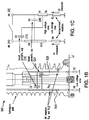
- Figure 1B shows the switchgear 500 (specifically, one pole of the switchgear as shown in Figures 1A ) with two HV resistors 510, 520. Shown in this view are two parasitic capacitances 10, 20 which exist between the two resistors 510, 520.
- FIG. 1C shows a simplified circuit equivalent with Resistive Voltage Dividers (RVDs) being formed by the HV resistors 510, 520 of Figure 1A and resistors R3, R4, and also showing the parasitic capacitances 10, 20.
- RVDs Resistive Voltage Dividers
- Figure 2 shows a representative illustration of the effects on a particular voltage measurement V2 on the load side in a multi-phase electrical system such as switchgear 500, of the voltage V1 on the source side of the same phase, as well as the voltages U1, U2, W1, W2 of the source side and load side of the other 2 phases.
- a multi-phase electrical system such as switchgear 500
- V2 the voltage V2 will be affected by the presence of these other voltages (VI, U1, U2, W1, W2), resulting in an error in the measured voltage.
- This error can adversely affect the operation of the electrical system 500, for example, preventing the safe implementation of "Sync Check" to ensure safe operation of switches in the system.
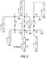
- FIG 3 shows an equivalent circuit of the electrical system of Figures 1A , 1B and 1C , to illustrate a step of measuring the effects of different voltages on a measured voltage according to some aspects.
- the effects of the voltage VI, on the measured voltage V2measured is performed by injecting a known reference voltage signal V1 in the circuit as shown.
- R3 is the resistance of the voltage measurement circuit.
- voltage measurement errors are used to characterise each electrical system (e.g. a switchgear) to allow the generation of an algorithm for use in providing compensated voltage measurements for each terminal or bushing of the electrical system 500.
- electrical system e.g. a switchgear
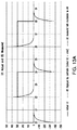
- Figure 4 shows a plot of the waveform of injected reference voltage V1 and the resulting measured voltage V2measured from Figure 3 . From this plot, characteristics of the error waveform (V2measured) can be determined for use in characterising the electrical system and calculating coefficients for use in an algorithm for providing a compensated voltage measurement.
- a value K being the ratio of the injected signal V1 and the error signal of V2measured can be determined, as can the phase difference ⁇ between the injected reference signal V1 and the error signal of V2measured.
- the error signal resulting from the crosstalk is also referred to as the capacitively coupled voltage or Vcrosstalk, and which is the signal measured during this characterisation phase with the measured terminal connected to earth.
- these values can be used in a number of different ways to provide a compensated voltage measurement to remove at least a portion of the error signal introduced by the crosstalk effect, as will be described in more detail below.
- Figures 3 and 4 show the procedure to determine the effect of V1 on measured voltage V2. To take into account the effects of all voltages in the electrical system on V2, the same procedure is undertaken for all other voltages. For example to determine the effect of U1 on V2, a reference signal U1 is injected at the terminal for U1, with all other terminals or bushing connected to ground, and the signal at V2 is measured. These results provide waveforms as shown in Figure 4 , with injected signal U1 instead of injected signal V1.
- a calibration step can be carried out prior to beginning the procedures described above to ensure that all phases are receiving the same injected voltage.
- the calibration step may be done after the crosstalk compensation.
- a method of obtaining characteristic measurements K and ⁇ of an electrical system comprising at least two terminals (in some embodiments, there are at least three terminals, including a common terminal), the method comprising, at step 600, injecting a reference voltage at a first of the at least two terminals; at step 610, measuring a capacitively coupled voltage at a second of the at least two terminals to provide an capacitively coupled voltage, the second terminal being connected to earth; at step 620, measuring a ratio of amplitude between the injected reference voltage and the capacitively coupled voltage to provide a K value; and at step 630, measuring a phase angle difference between the injected reference voltage and the capacitively coupled voltage to provide an angle value ⁇ .
- the above steps are carried out for each terminal pair so as to obtain a K value and an angle ⁇ value for each terminal pair as previously described.
- the above steps are carried out twice, one for T1T2 (i.e. inject reference voltage V ref at T1 and measure capacitively coupled voltage V crosstalk at T2) and once for T2T1 (i.e. inject reference voltage V ref at T2 and measure capacitively coupled voltage V crosstalk at T1).
- T1T2 i.e. inject reference voltage V ref at T1 and measure capacitively coupled voltage V crosstalk at T2
- T2T1 i.e. inject reference voltage V ref at T2 and measure capacitively coupled voltage V crosstalk at T1
- the pairings will be T1T2, T2T1, T2T3, T3T2, T1T3 and T3T1.
- V1 is the voltage at terminal T1
- V2 is the voltage at terminal T2 etc.
- V1V2 V1 on V2
- V1V2 W1 on V2
- U1V2 U1V2
- the K and ⁇ values obtained from the above process can be used to determine compensation coefficients for use in a compensation algorithm as shown in equation 1:
- V 2 comp V 2 measured ⁇ KC U 1 V 2 ⁇ dU 1 ⁇ K 2 U 1 V 2 ⁇ dV 2 dt + KC V 1 V 2 ⁇ dV 1 ⁇ K 2 V 1 V 2 d ⁇ V 2 dt + KC W 1 V 2 ⁇ dW 1 ⁇ K 2 W 1 V 2 ⁇ dV 2 dt + KC U 2 V 2 ⁇ dU 2 ⁇ K 2 U 2 V 2 ⁇ dV 2 dt + KC W 2 V 2 ⁇ dW 2 ⁇ K 2 W 2 V 2 ⁇ dV 2 dt
- the above equation can be used in real time as a voltage measurement is taken of the electrical assembly in use.
- a calculation is made to determine the voltage variation (dv) difference with the previous sample taken., which provides the dv/dt values for the equation above.
- the time difference between raw voltage measurements is provided by the sampling rate of the device making the measurements as will be described in more detail further below.
- V 2 comp V 2 measured ⁇ P V 1 V 2 K 1 V 1 V 2 ⁇ Sin ⁇ ⁇ dV 1 ⁇ K 2 V 1 V 2 ⁇ dV 2 dt + Cos ⁇ ⁇ V 1 ⁇ K 2 V 1 V 2 ⁇ V 2 where:
- equation (3) can be modified to remove only the capacitive component of the error from the crosstalk, and can be simplified to:
- V 2 comp V 2 measured ⁇ P U 1 V 2 ⁇ K 1 U 1 V 2 dU 1 ⁇ K 2 U 1 V 2 ⁇ dV 2 dt + P V 1 V 2 ⁇ K 1 V 1 V 2 ⁇ dV 1 ⁇ K 2 V 1 V 2 ⁇ dV 2 dt + P W 1 V 2 ⁇ K 1 W 2 V 2 ⁇ dW 1 ⁇ K 2 W 1 V 2 ⁇ dV 2 dt + P U 2 V 2 ⁇ K 1 U 2 V 2 ⁇ dU 2 ⁇ K 2 U 2 V 2 ⁇ dV 2 dt + P W 2 V 2 ⁇ K 1 W 2 V 2 ⁇ dW 2 ⁇ K 2 W 2 V 2 ⁇ dV 2 dt + P U 2 V 2 ⁇ K 1 U 2 V 2 ⁇ dU 2 ⁇ K 2 U 2 V 2 ⁇ dV 2
- the compensated values may then be stored in memory, displayed on a display screen and/or used in controlling further functions of the electrical system 500 such as Sync check.
- This compensating procedure can be used to provide more accurate voltage measurements in real time as the electrical system 500 (being in this example, the full recloser system 500 shown in Figure 1A ) is operating, so as to reduce deleterious effects of crosstalk on the voltage measurements in functions such as Sync check.
- the utility adjusts the amplitude and waits for the signal to be in phase before closing the switch. Without the compensation, the amplitude would not be reliable in this situation.
- an improved compensated V2 measurement can be obtained by considering only the effects of U1 and V1, or W1 and V1 or U2 and W2.
- any consideration of the effect of any one or more other voltages on a measured voltage and removal of at least a part of that effect, will provide a voltage value closer to the real value and thus provide a benefit.
- V 2 comp 2 V 2 measured ⁇ KcU 1 V 2 ⁇ dU 1 comp ⁇ k 2 U 1 V 2 ⁇ dV 2 comp dt + KcV 1 V 2 ⁇ dV 1 comp ⁇ k 2 V 1 V 2 ⁇ dV 2 comp dt + KcW 1 V 2 ⁇ dW 1 comp ⁇ k 2 W 1 V 2 dV 2 comp dt + KcU 2 V 2 ⁇ dU 2 comp ⁇ k 2 U 2 V 2 ⁇ dV 2 comp dt + KcW 2 V 2 ⁇ dW 2 comp ⁇ k 2 W 2 V 2 ⁇ dV 2 comp dt
- the resistive effect is negligible as described above, and be ignored.
- the measured angle ⁇ value is lower, such as between about 30° and about 40°, between about 40° and about 50°, between about 50° and about 60° and between about 60° and about 70°
- the resistive effect is more prevalent and can be taken into account when removing the error signal. It will be appreciated that for each electrical system and DSP capabilities available, a determination may be made as to what angle will be considered to be sufficiently close to 90 degrees so as to ignore the resistive component.
- V 2 comp V 2 measured ⁇ [ KC V 1 V 2 ⁇ dV 1 ⁇ K 2 V 1 V 2 ⁇ dV 2 dt + V 1 ⁇ K 2 V 1 V 2 ⁇ V 2 KR V 1 V 2
- V 2 comp V 2 measured ⁇ Kc U 1 V 2 ⁇ dU 1 ⁇ K 2 U 1 V 2 ⁇ dV 2 dt + Kc V 1 V 2 ⁇ dV 1 ⁇ K 2 V 1 V 2 ⁇ dV 2 dt + Kc W 1 V 2 ⁇ dW 1 ⁇ K 2 W 1 V 2 ⁇ dV 2 dt + Kc U 2 V 2 ⁇ dU 2 ⁇ K 2 U 2 V 2 ⁇ dV 2 dt + Kc W 2 V 2 ⁇ dW 2 ⁇ K 2 W 2 V 2 ⁇ dV 2 dt + U 1 ⁇ K 2 U 1 V 2 ⁇ V 2 KR U 1 V 2 + V 1 ⁇ K 2 V 1 V 2 ⁇ V 2 KR V 1 V 2 + W 1 ⁇ K 2 W 1 V 2 ⁇ V 2 KR W 1 V 2 + U 2 ⁇ K 2 U 1 V 2 ⁇ V 2 KR U 1 V 2 + V 1 ⁇ K 2 V 1 V 2 ⁇
- V 2 comp 2 V 2 measured ⁇ KcU 1 V 2 ⁇ dU 1 comp ⁇ k 2 U 1 V 2 ⁇ dV 2 comp dt + KcV 1 V 2 ⁇ dV 1 comp ⁇ k 2 V 1 V 2 ⁇ dV 2 comp dt + KcV 1 V 2 ⁇ dW 1 comp ⁇ k 2 V 1 V 2 ⁇ dV 2 comp dt + KcW 2 V 2 ⁇ dU 2 comp ⁇ k 2 W 2 V 2 ⁇ dV 2 comp dt + KcU 2 V 2 ⁇ dW 2 comp ⁇ k 2 U 2 V 2 ⁇ dV 2 comp dt + KcW 2 V 2 ⁇ dW 2 comp ⁇ k 2 W 2 V 2 ⁇ dV 2 comp dt + U 1 comp ⁇ K 2 U 1 V 2 ⁇ V 2 comp KR U 1 V 2 + V 1 comp ⁇ K 2 V 1 V 2 ⁇ V 2 comp KR U 1 V 2 + V
- the K and ⁇ values obtained as previously described may be used to characterise the electrical system by explicitly calculating the values of all of the internal impedances R1, R5 and C of the electrical system. These calculated impedance values may then be used to derive the compensation coefficients as described below.
- Figures 6 to 11 are used to derive these impedance values.
- Figure 6 shows a simpler representation of the circuit equivalent of Figure 1B .
- Figure 7 shows the circuit of Figure 6 showing one source V1 and one resulting crosstalk V2 .
- Figure 8 shows an equivalent schematic for one phase of the electrical system or switchgear 500 and Figure 9 shows this simplified schematic transformed into an equivalent Thevenin model.
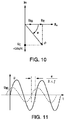
- Figure 10 shows a phasor diagram for U and Figure 11 shows the waveforms for the components U and U R3 .
- E A .
- i 1 Kc dUc / dt
- Uc U - U R
- U V1 - k2.V2
- the measurement resistor values R3 are much smaller than the HV resistors R1 and R5, i.e. R3 is negligible. It will also be appreciated that usually, Zc ⁇ R therefore Uc ⁇ U. In this case, the effect of R on the crosstalk is negligible and the crosstalk is predominantly capacitive.
- An equivalent circuit of the electrical system can be generated, and, knowing the input parameters Input voltage, frequency, percentage of crosstalk measured (K), angle ⁇ measured), RVD and R3, all of the internal impedances R1, R5 and C can be calculated.
- impedances of the circuit may be calculated by injecting a step function at U1 and measuring the impulse response at U2 with the U2 terminal grounded as previously described with reference to Figures 2 to 4 .
- the waveforms of Figure 4 are replaced by the waveforms shown in Figures 13A and 13B .
- V 2 comp V 2 measured ⁇ KC U 1 V 2 ⁇ dU 1 dt ⁇ K 2 U 1 V 2 dV 2 dt + KC V 1 V 2 ⁇ dV 1 dt ⁇ K 2 V 1 V 2 dV 2 dt + KC W 1 V 2 ⁇ dW 1 dt ⁇ K 2 w 1 V 2 dV 2 dt + KC U 2 V 2 ⁇ dU 2 dt ⁇ K 2 u 2 V 2 dV 2 dt + KC W 2 V 2 ⁇ kV 2 dt dW 2 dt ⁇ K 2 w 2 V 2
- V 2 comp V 2 measured ⁇ KC U 1 V 2 ⁇ dU 1 dt ⁇ dV 2 dt + KC V 1 V 2 ⁇ dV 1 dt ⁇ dV 2 dt + KC W 1 V 2 ⁇ dW 1 dt ⁇ dV 2 dt + KC U 2 V 2 ⁇ dU 2 dt ⁇ dV 2 dt + KC W 2 V 2 ⁇ dW 2 dt ⁇ dV 2 dt ⁇ dV 2 dt
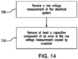
- a method of providing a compensated voltage measurement of a voltage measurement in an electrical system that includes an error from crosstalk comprising, in step 700, receiving a raw voltage measurement of the electrical system; and, in step 710, removing at least a capacitive component of the error from the crosstalk to provide the compensated voltage measurement.
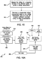
- a method for providing a compensated voltage measurement of a voltage measurement in an electrical system comprising, in step 800, measuring the voltage at a measuring terminal of the electrical system to provide the voltage measurement, and, in step 810, determining the compensated voltage measurement based on the voltage measurement and on at last one crosstalk coefficient calculated during an initial characterisation phase.
- this initial characterisation phase comprises, injecting a reference voltage signal at a first terminal of the electrical system; measuring at the terminal, a capacitively coupled signal, from the reference voltage signal; comparing the reference voltage signal with a measured capacitively coupled signal; and calculating the at least one crosstalk coefficient base on the comparison of the reference voltage signal and the measured capacitively coupled signal.
- a controller 200 for use with the electrical system/switchgear 500 to effect the voltage compensation as described in the various aspects above.
- the controller 200 comprises an input having a filter and surge protection unit 210 for receiving the analog voltage measurements from the terminals or bushings of the electrical system such as a switchgear, , or recloser 500. These raw measurements are provided to the A/D converter, which in some embodiments, as shown in Figure 16A is provided by device ADS13XE0X (16ks/s), provided by Texas Instruments, Inc.
- DSP digital signal processor
- the controller 200 of Figure 16A also includes EEProm 240, Flash memory 250, and a main processor 260, which in this embodiment is provided by Sitara ARM Cortex AM3358 processor provided by Texas Instruments, Inc.
- the various blocks are powered by power supply 280 controlled by power supply supervisor 270, provided by device TPS65218 provided by Texas Instruments, Inc.
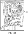
- Figure 16B shows a photograph of an example switchgear controller 200 having the structure shown and described with reference to Figure 16A .
- Figure 17 shows an embodiment of the device 200 receiving voltage output data from electrical system 500, such as an electrical switchgear such as a recloser or RVD.
- Figure 17 shows the measured voltages Vmeas for each of U1, U2, VI, V2, W1 and W2 output from electrical system 500 and input to device 200.
- the output of device 200 is the compensated voltage measurements Vcomp for each of U1, U2, VI, V2, W1 and W2.
- the compensated voltage measurements are then used to control aspects of the electrical system as previously described.
- Figure 18A shows a waveform of a measured voltage signal V2 measured at the V2 terminal of the electrical system (which is the input to filter 210 of device 200). As will be appreciated, this measurement will contain the error E from the crosstalk from each of the other voltages VI, U1, U2, W1 and W2.
- Figure 18B shows the compensated voltage V2comp resulting from the application of the one or more methods described above, which effectively removes the, or part of the, crosstalk error, thus providing a voltage measurement that is closer to the real voltage appearing at the V2 terminal than was measured by the device.
- This compensated voltage measurement can then be used to control one or more functions of the electrical system 500 such as Sync Check, or any other function that requires an accurate measurement of the voltages.
- a device for controlling an electrical system based on one or more voltage measurements of the electrical system comprising; an input for receiving data corresponding to the one or more voltage measurements; a data processor for processing the received data and for generating data corresponding to a compensated voltage measurement; and an output for controlling the electrical system according to the compensated voltage measurement; wherein the processor contains executable software for causing the processor to perform one or more of the methods described above.
- non-transitory computer-readable medium containing executable code for causing a processor to perform one or more of the methods described above.
- Figure 19 shows an expanded Thevenin equivalent circuit of that shown in Figure 9 .
- R 2 U 2 2.
- RVD RVD ⁇ 4 R D 2 . RVD ⁇ R 2 . RVD ⁇ 2 R . D 2 D 2 2
- RVD 2 . R 2 + 4D 2 . RVD. R + 4D 4 - 2D 2 RVD 2 0
- R ⁇ 4 D 2 . RVD ⁇ 8 D 2 . RVD 4 2 RVD 2
- the crosstalk compensation algorithm in its various forms described above works by simulating the error, then removing it from the measured value. This simulation can be simplified to only include one pole and the effect of one side to the other (e.g. V1 on V2). The different calculations for each pole pairing can then be combined in the algorithm as previously described.
- the algorithm is based on the following equations, which are based on the Thevenin model of Figure 19 :
- Uc 1 / C ⁇ ⁇ i . dt using ⁇ i . dt calculated up to the previous sample
- Factor K1 can be calculated as below:
- processing may be implemented within one or more application specific integrated circuits (ASICs), digital signal processors (DSPs), digital signal processing devices (DSPDs), programmable logic devices (PLDs), field programmable gate arrays (FPGAs), processors, controllers, micro-controllers, microprocessors, other electronic units designed to perform the functions described herein, or a combination thereof.
- ASICs application specific integrated circuits
- DSPs digital signal processors
- DSPDs digital signal processing devices
- PLDs programmable logic devices
- FPGAs field programmable gate arrays
- processors controllers, micro-controllers, microprocessors, other electronic units designed to perform the functions described herein, or a combination thereof.
- Software modules also known as computer programs, computer codes, or instructions, may contain a number a number of source code or object code segments or instructions, and may reside in any computer readable medium such as a RAM memory, flash memory, ROM memory, EPROM memory, registers, hard disk, a removable disk, a CD-ROM, a DVD-ROM, a Blu-ray disc, or any other form of computer readable medium.
- the computer-readable media may comprise non-transitory computer-readable media (e.g., tangible media).
- computer-readable media may comprise transitory computer- readable media (e.g., a signal). Combinations of the above should also be included within the scope of computer-readable media.
- the computer readable medium may be integral to the processor.
- the processor and the computer readable medium may reside in an ASIC or related device.
- the software codes may be stored in a memory unit and the processor may be configured to execute them.
- the memory unit may be implemented within the processor or external to the processor, in which case it can be communicatively coupled to the processor via various means as is known in the art.
- modules and/or other appropriate means for performing the methods and techniques described herein can be downloaded and/or otherwise obtained by computing device.
- a device can be coupled to a server to facilitate the transfer of means for performing the methods described herein.
- various methods described herein can be provided via storage means (e.g., RAM, ROM, a physical storage medium such as a compact disc (CD) or floppy disk, etc.), such that a computing device can obtain the various methods upon coupling or providing the storage means to the device.
- storage means e.g., RAM, ROM, a physical storage medium such as a compact disc (CD) or floppy disk, etc.
- one aspect may comprise a computer program product for performing the method or operations presented herein.
- a computer program product may comprise a computer (or processor) readable medium having instructions stored (and/or encoded) thereon, the instructions being executable by one or more processors to perform the operations described herein.
- the computer program product may include packaging material.
- the methods disclosed herein comprise one or more steps or actions for achieving the described method.
- the method steps and/or actions may be interchanged with one another without departing from the scope of the claims.
- the order and/or use of specific steps and/or actions may be modified without departing from the scope of the claims.
- the system may be a computer implemented system comprising of a display device, a processor and a memory and an input device.
- the memory may comprise instructions to cause the processor to execute a method described herein.
- the processor memory and display device may be included in a standard computing device, such as a desktop computer, a portable computing device such as a laptop computer or tablet, or they may be included in a customised device or system.
- the computing device may be a unitary computing or programmable device, or a distributed device comprising several components operatively (or functionally) connected via wired or wireless connections.
- An embodiment of a computing device comprises a central processing unit (CPU), a memory, a display apparatus, and may include an input device such as keyboard, mouse, etc.
- the CPU comprises an Input/Output Interface, an Arithmetic and Logic Unit (ALU) and a Control Unit and Program Counter element which is in communication with input and output devices (eg input device and display apparatus) through the Input/Output Interface.
- the Input/Output Interface may comprise a network interface and/or communications module for communicating with an equivalent communications module in another device using a predefined communications protocol (e.g. Bluetooth, Zigbee, IEEE 802.15, IEEE 802.11, TCP/IP, UDP, etc).
- a graphical processing unit (GPU) may also be included.
- the display apparatus may comprise a flat screen display (eg LCD, LED, plasma, touch screen, etc), a projector, CRT, etc.
- the computing device may comprise a single CPU (core) or multiple CPU's (multiple core), or multiple processors.
- the computing device may use a parallel processor, a vector processor, or be a distributed computing device.
- the memory is operatively coupled to the processor(s) and may comprise RAM and ROM components, and may be provided within or external to the device.
- the memory may be used to store the operating system and additional software modules or instructions.
- the processor(s) may be configured to load and executed the software modules or instructions stored in the memory.
Landscapes
- Physics & Mathematics (AREA)
- General Physics & Mathematics (AREA)
- Engineering & Computer Science (AREA)
- Power Engineering (AREA)
- Measurement Of Resistance Or Impedance (AREA)
- Measurement Of Current Or Voltage (AREA)
- Measuring Instrument Details And Bridges, And Automatic Balancing Devices (AREA)
Applications Claiming Priority (2)
| Application Number | Priority Date | Filing Date | Title |
|---|---|---|---|
| AU2019901217A AU2019901217A0 (en) | 2019-04-09 | Voltage measurement compensation in high voltage systems | |
| AU2019203600A AU2019203600B2 (en) | 2019-04-09 | 2019-05-22 | Voltage measurement compensation in high voltage systems |
Publications (3)
| Publication Number | Publication Date |
|---|---|
| EP3722819A2 true EP3722819A2 (de) | 2020-10-14 |
| EP3722819A3 EP3722819A3 (de) | 2020-12-23 |
| EP3722819B1 EP3722819B1 (de) | 2023-05-10 |
Family
ID=69844418
Family Applications (1)
| Application Number | Title | Priority Date | Filing Date |
|---|---|---|---|
| EP20162904.5A Active EP3722819B1 (de) | 2019-04-09 | 2020-03-13 | Spannungsmesskompensation in hochspannungssystemen |
Country Status (4)
| Country | Link |
|---|---|
| US (1) | US11674986B2 (de) |
| EP (1) | EP3722819B1 (de) |
| CN (1) | CN111796141B (de) |
| ES (1) | ES2947771T3 (de) |
Cited By (1)
| Publication number | Priority date | Publication date | Assignee | Title |
|---|---|---|---|---|
| CN113589025A (zh) * | 2021-07-07 | 2021-11-02 | 广东电网能源发展有限公司 | 电气试验计算方法、装置、设备和介质 |
Families Citing this family (1)
| Publication number | Priority date | Publication date | Assignee | Title |
|---|---|---|---|---|
| CN121909400A (zh) * | 2023-09-25 | 2026-04-21 | 西门子能源国际公司 | 用于串扰补偿的方法和补偿电路 |
Family Cites Families (10)
| Publication number | Priority date | Publication date | Assignee | Title |
|---|---|---|---|---|
| US6717395B2 (en) | 2001-05-31 | 2004-04-06 | Mcgraw-Edison Company | Current transformer based high voltage measurement apparatus |
| US6529013B2 (en) * | 2001-05-31 | 2003-03-04 | Mcgraw-Edison Company | Three-phase voltage sensor with active crosstalk cancellation |
| CN1997900B (zh) * | 2004-05-25 | 2010-10-13 | 埃内尔迪斯特里布齐恩公司 | 用于检测任意未知相电压相对于参考相电压的相配线的方法和装置 |
| PL1936391T3 (pl) * | 2006-12-19 | 2011-08-31 | Abb Schweiz Ag | Urządzenie i sposób poprawiania dokładności przekładników |
| FR3005744B1 (fr) | 2013-05-14 | 2015-08-21 | Airbus Operations Sas | Systeme et procede de test d'integrite d'un reseau electrique dans un aeronef |
| CA2939796A1 (en) | 2014-02-20 | 2015-08-27 | Cooper Technologies Company | Modular switchgear insulation system |
| US10545182B2 (en) * | 2016-03-17 | 2020-01-28 | Texas Instruments Incorporated | Crosstalk calibration for multi-channel systems |
| CN106226590A (zh) * | 2016-07-19 | 2016-12-14 | 国网河北省电力公司电力科学研究院 | 一种电力系统同步相量测量方法 |
| CN109038599A (zh) * | 2018-06-22 | 2018-12-18 | 国网湖南省电力有限公司 | 一种无功补偿优化配置方法及系统 |
| US10840971B2 (en) * | 2018-08-21 | 2020-11-17 | Micron Technology, Inc. | Pre-distortion for multi-level signaling |
-
2019
- 2019-09-23 US US16/578,803 patent/US11674986B2/en active Active
-
2020
- 2020-03-13 EP EP20162904.5A patent/EP3722819B1/de active Active
- 2020-03-13 ES ES20162904T patent/ES2947771T3/es active Active
- 2020-04-08 CN CN202010268093.1A patent/CN111796141B/zh active Active
Cited By (1)
| Publication number | Priority date | Publication date | Assignee | Title |
|---|---|---|---|---|
| CN113589025A (zh) * | 2021-07-07 | 2021-11-02 | 广东电网能源发展有限公司 | 电气试验计算方法、装置、设备和介质 |
Also Published As
| Publication number | Publication date |
|---|---|
| CN111796141A (zh) | 2020-10-20 |
| US11674986B2 (en) | 2023-06-13 |
| ES2947771T3 (es) | 2023-08-18 |
| EP3722819B1 (de) | 2023-05-10 |
| US20200326360A1 (en) | 2020-10-15 |
| EP3722819A3 (de) | 2020-12-23 |
| CN111796141B (zh) | 2025-03-11 |
Similar Documents
| Publication | Publication Date | Title |
|---|---|---|
| Beites et al. | Harmonics, interharmonics and unbalances of arc furnaces: A new frequency domain approach | |
| CN103983942B (zh) | 一种虚实负荷可切换的智能电能表检定装置及其方法 | |
| CN105723229A (zh) | 一种适用于p类相量测量单元pmu的同步相量测量方法 | |
| EP3722819B1 (de) | Spannungsmesskompensation in hochspannungssystemen | |
| CN105510719A (zh) | 三相电网谐波阻抗测量方法 | |
| CN110909497A (zh) | 一种高压开关设备在冲击电压下的暂态电场计算方法 | |
| CN110865238A (zh) | 一种基于准谐波模型采样算法的交流电阻测量方法及装置 | |
| CN111141995A (zh) | 一种基于比幅原理的线路双端稳态量测距方法和系统 | |
| CN105403848A (zh) | 一种新型电容型设备在线监测系统校验装置 | |
| CN104237832B (zh) | 一种复阻抗标准器的校准方法及装置 | |
| CN107390032B (zh) | 线路对地电容参数测量系统及测量方法 | |
| JP2020076671A (ja) | 対地静電容量測定装置および対地静電容量測定方法 | |
| Li et al. | Full-wave simulation of system-level disruption during secondary ESD events in a smartphone | |
| AU2019203600B2 (en) | Voltage measurement compensation in high voltage systems | |
| CN113702714B (zh) | 一种用于测量直流电压互感器高压臂电容值的方法 | |
| CN113884739A (zh) | 一种宽频电压分压器装置及刻度因数标定方法 | |
| CN104833849B (zh) | 石英晶体串联谐振频率测试方法 | |
| Muntakim et al. | Insulation assessment based on dielectric dissipation factor measurement under non-sinusoidal excitation | |
| CN114646806B (zh) | 航天器直流负载输入阻抗测量方法及装置 | |
| JP2014115142A (ja) | 接地抵抗計および接地抵抗測定方法、ならびにプログラム | |
| JP5501820B2 (ja) | 線路特性演算装置および線路特性演算方法 | |
| CN106885939A (zh) | 低压电器短路耐受强度试验功率因数的三极值点测量方法 | |
| Ma et al. | Calibration of measuring network of leakage current tester by high frequency current source | |
| WO2008119389A1 (en) | Iterative method for characterizing the frequency dependence of the linear properties of an electrical component | |
| Šíra et al. | Modelling of PMU uncertainty by means of Monte Carlo method |
Legal Events
| Date | Code | Title | Description |
|---|---|---|---|
| PUAI | Public reference made under article 153(3) epc to a published international application that has entered the european phase |
Free format text: ORIGINAL CODE: 0009012 |
|
| STAA | Information on the status of an ep patent application or granted ep patent |
Free format text: STATUS: THE APPLICATION HAS BEEN PUBLISHED |
|
| AK | Designated contracting states |
Kind code of ref document: A2 Designated state(s): AL AT BE BG CH CY CZ DE DK EE ES FI FR GB GR HR HU IE IS IT LI LT LU LV MC MK MT NL NO PL PT RO RS SE SI SK SM TR |
|
| AX | Request for extension of the european patent |
Extension state: BA ME |
|
| PUAL | Search report despatched |
Free format text: ORIGINAL CODE: 0009013 |
|
| AK | Designated contracting states |
Kind code of ref document: A3 Designated state(s): AL AT BE BG CH CY CZ DE DK EE ES FI FR GB GR HR HU IE IS IT LI LT LU LV MC MK MT NL NO PL PT RO RS SE SI SK SM TR |
|
| AX | Request for extension of the european patent |
Extension state: BA ME |
|
| RIC1 | Information provided on ipc code assigned before grant |
Ipc: H01H 33/02 20060101ALI20201118BHEP Ipc: G01R 19/00 20060101AFI20201118BHEP Ipc: G01R 35/00 20060101ALI20201118BHEP |
|
| STAA | Information on the status of an ep patent application or granted ep patent |
Free format text: STATUS: REQUEST FOR EXAMINATION WAS MADE |
|
| 17P | Request for examination filed |
Effective date: 20210601 |
|
| RBV | Designated contracting states (corrected) |
Designated state(s): AL AT BE BG CH CY CZ DE DK EE ES FI FR GB GR HR HU IE IS IT LI LT LU LV MC MK MT NL NO PL PT RO RS SE SI SK SM TR |
|
| GRAP | Despatch of communication of intention to grant a patent |
Free format text: ORIGINAL CODE: EPIDOSNIGR1 |
|
| STAA | Information on the status of an ep patent application or granted ep patent |
Free format text: STATUS: GRANT OF PATENT IS INTENDED |
|
| INTG | Intention to grant announced |
Effective date: 20230222 |
|
| GRAS | Grant fee paid |
Free format text: ORIGINAL CODE: EPIDOSNIGR3 |
|
| GRAA | (expected) grant |
Free format text: ORIGINAL CODE: 0009210 |
|
| STAA | Information on the status of an ep patent application or granted ep patent |
Free format text: STATUS: THE PATENT HAS BEEN GRANTED |
|
| AK | Designated contracting states |
Kind code of ref document: B1 Designated state(s): AL AT BE BG CH CY CZ DE DK EE ES FI FR GB GR HR HU IE IS IT LI LT LU LV MC MK MT NL NO PL PT RO RS SE SI SK SM TR |
|
| REG | Reference to a national code |
Ref country code: GB Ref legal event code: FG4D |
|
| REG | Reference to a national code |
Ref country code: AT Ref legal event code: REF Ref document number: 1567188 Country of ref document: AT Kind code of ref document: T Effective date: 20230515 Ref country code: CH Ref legal event code: EP |
|
| REG | Reference to a national code |
Ref country code: DE Ref legal event code: R096 Ref document number: 602020010589 Country of ref document: DE |
|
| REG | Reference to a national code |
Ref country code: IE Ref legal event code: FG4D |
|
| REG | Reference to a national code |
Ref country code: ES Ref legal event code: FG2A Ref document number: 2947771 Country of ref document: ES Kind code of ref document: T3 Effective date: 20230818 |
|
| REG | Reference to a national code |
Ref country code: LT Ref legal event code: MG9D |
|
| REG | Reference to a national code |
Ref country code: NL Ref legal event code: MP Effective date: 20230510 |
|
| REG | Reference to a national code |
Ref country code: AT Ref legal event code: MK05 Ref document number: 1567188 Country of ref document: AT Kind code of ref document: T Effective date: 20230510 |
|
| PG25 | Lapsed in a contracting state [announced via postgrant information from national office to epo] |
Ref country code: SE Free format text: LAPSE BECAUSE OF FAILURE TO SUBMIT A TRANSLATION OF THE DESCRIPTION OR TO PAY THE FEE WITHIN THE PRESCRIBED TIME-LIMIT Effective date: 20230510 Ref country code: PT Free format text: LAPSE BECAUSE OF FAILURE TO SUBMIT A TRANSLATION OF THE DESCRIPTION OR TO PAY THE FEE WITHIN THE PRESCRIBED TIME-LIMIT Effective date: 20230911 Ref country code: NO Free format text: LAPSE BECAUSE OF FAILURE TO SUBMIT A TRANSLATION OF THE DESCRIPTION OR TO PAY THE FEE WITHIN THE PRESCRIBED TIME-LIMIT Effective date: 20230810 Ref country code: NL Free format text: LAPSE BECAUSE OF FAILURE TO SUBMIT A TRANSLATION OF THE DESCRIPTION OR TO PAY THE FEE WITHIN THE PRESCRIBED TIME-LIMIT Effective date: 20230510 Ref country code: AT Free format text: LAPSE BECAUSE OF FAILURE TO SUBMIT A TRANSLATION OF THE DESCRIPTION OR TO PAY THE FEE WITHIN THE PRESCRIBED TIME-LIMIT Effective date: 20230510 |
|
| PG25 | Lapsed in a contracting state [announced via postgrant information from national office to epo] |
Ref country code: RS Free format text: LAPSE BECAUSE OF FAILURE TO SUBMIT A TRANSLATION OF THE DESCRIPTION OR TO PAY THE FEE WITHIN THE PRESCRIBED TIME-LIMIT Effective date: 20230510 Ref country code: PL Free format text: LAPSE BECAUSE OF FAILURE TO SUBMIT A TRANSLATION OF THE DESCRIPTION OR TO PAY THE FEE WITHIN THE PRESCRIBED TIME-LIMIT Effective date: 20230510 Ref country code: LV Free format text: LAPSE BECAUSE OF FAILURE TO SUBMIT A TRANSLATION OF THE DESCRIPTION OR TO PAY THE FEE WITHIN THE PRESCRIBED TIME-LIMIT Effective date: 20230510 Ref country code: LT Free format text: LAPSE BECAUSE OF FAILURE TO SUBMIT A TRANSLATION OF THE DESCRIPTION OR TO PAY THE FEE WITHIN THE PRESCRIBED TIME-LIMIT Effective date: 20230510 Ref country code: IS Free format text: LAPSE BECAUSE OF FAILURE TO SUBMIT A TRANSLATION OF THE DESCRIPTION OR TO PAY THE FEE WITHIN THE PRESCRIBED TIME-LIMIT Effective date: 20230910 Ref country code: HR Free format text: LAPSE BECAUSE OF FAILURE TO SUBMIT A TRANSLATION OF THE DESCRIPTION OR TO PAY THE FEE WITHIN THE PRESCRIBED TIME-LIMIT Effective date: 20230510 Ref country code: GR Free format text: LAPSE BECAUSE OF FAILURE TO SUBMIT A TRANSLATION OF THE DESCRIPTION OR TO PAY THE FEE WITHIN THE PRESCRIBED TIME-LIMIT Effective date: 20230811 |
|
| PG25 | Lapsed in a contracting state [announced via postgrant information from national office to epo] |
Ref country code: FI Free format text: LAPSE BECAUSE OF FAILURE TO SUBMIT A TRANSLATION OF THE DESCRIPTION OR TO PAY THE FEE WITHIN THE PRESCRIBED TIME-LIMIT Effective date: 20230510 |
|
| PG25 | Lapsed in a contracting state [announced via postgrant information from national office to epo] |
Ref country code: SK Free format text: LAPSE BECAUSE OF FAILURE TO SUBMIT A TRANSLATION OF THE DESCRIPTION OR TO PAY THE FEE WITHIN THE PRESCRIBED TIME-LIMIT Effective date: 20230510 |
|
| PG25 | Lapsed in a contracting state [announced via postgrant information from national office to epo] |
Ref country code: SM Free format text: LAPSE BECAUSE OF FAILURE TO SUBMIT A TRANSLATION OF THE DESCRIPTION OR TO PAY THE FEE WITHIN THE PRESCRIBED TIME-LIMIT Effective date: 20230510 Ref country code: SK Free format text: LAPSE BECAUSE OF FAILURE TO SUBMIT A TRANSLATION OF THE DESCRIPTION OR TO PAY THE FEE WITHIN THE PRESCRIBED TIME-LIMIT Effective date: 20230510 Ref country code: RO Free format text: LAPSE BECAUSE OF FAILURE TO SUBMIT A TRANSLATION OF THE DESCRIPTION OR TO PAY THE FEE WITHIN THE PRESCRIBED TIME-LIMIT Effective date: 20230510 Ref country code: EE Free format text: LAPSE BECAUSE OF FAILURE TO SUBMIT A TRANSLATION OF THE DESCRIPTION OR TO PAY THE FEE WITHIN THE PRESCRIBED TIME-LIMIT Effective date: 20230510 Ref country code: DK Free format text: LAPSE BECAUSE OF FAILURE TO SUBMIT A TRANSLATION OF THE DESCRIPTION OR TO PAY THE FEE WITHIN THE PRESCRIBED TIME-LIMIT Effective date: 20230510 Ref country code: CZ Free format text: LAPSE BECAUSE OF FAILURE TO SUBMIT A TRANSLATION OF THE DESCRIPTION OR TO PAY THE FEE WITHIN THE PRESCRIBED TIME-LIMIT Effective date: 20230510 |
|
| REG | Reference to a national code |
Ref country code: DE Ref legal event code: R097 Ref document number: 602020010589 Country of ref document: DE |
|
| PLBE | No opposition filed within time limit |
Free format text: ORIGINAL CODE: 0009261 |
|
| STAA | Information on the status of an ep patent application or granted ep patent |
Free format text: STATUS: NO OPPOSITION FILED WITHIN TIME LIMIT |
|
| 26N | No opposition filed |
Effective date: 20240213 |
|
| PG25 | Lapsed in a contracting state [announced via postgrant information from national office to epo] |
Ref country code: SI Free format text: LAPSE BECAUSE OF FAILURE TO SUBMIT A TRANSLATION OF THE DESCRIPTION OR TO PAY THE FEE WITHIN THE PRESCRIBED TIME-LIMIT Effective date: 20230510 |
|
| PG25 | Lapsed in a contracting state [announced via postgrant information from national office to epo] |
Ref country code: SI Free format text: LAPSE BECAUSE OF FAILURE TO SUBMIT A TRANSLATION OF THE DESCRIPTION OR TO PAY THE FEE WITHIN THE PRESCRIBED TIME-LIMIT Effective date: 20230510 |
|
| REG | Reference to a national code |
Ref country code: CH Ref legal event code: PL |
|
| PG25 | Lapsed in a contracting state [announced via postgrant information from national office to epo] |
Ref country code: BG Free format text: LAPSE BECAUSE OF FAILURE TO SUBMIT A TRANSLATION OF THE DESCRIPTION OR TO PAY THE FEE WITHIN THE PRESCRIBED TIME-LIMIT Effective date: 20230510 |
|
| PG25 | Lapsed in a contracting state [announced via postgrant information from national office to epo] |
Ref country code: LU Free format text: LAPSE BECAUSE OF NON-PAYMENT OF DUE FEES Effective date: 20240313 |
|
| PG25 | Lapsed in a contracting state [announced via postgrant information from national office to epo] |
Ref country code: MC Free format text: LAPSE BECAUSE OF FAILURE TO SUBMIT A TRANSLATION OF THE DESCRIPTION OR TO PAY THE FEE WITHIN THE PRESCRIBED TIME-LIMIT Effective date: 20230510 |
|
| PG25 | Lapsed in a contracting state [announced via postgrant information from national office to epo] |
Ref country code: MC Free format text: LAPSE BECAUSE OF FAILURE TO SUBMIT A TRANSLATION OF THE DESCRIPTION OR TO PAY THE FEE WITHIN THE PRESCRIBED TIME-LIMIT Effective date: 20230510 Ref country code: LU Free format text: LAPSE BECAUSE OF NON-PAYMENT OF DUE FEES Effective date: 20240313 Ref country code: BG Free format text: LAPSE BECAUSE OF FAILURE TO SUBMIT A TRANSLATION OF THE DESCRIPTION OR TO PAY THE FEE WITHIN THE PRESCRIBED TIME-LIMIT Effective date: 20230510 |
|
| REG | Reference to a national code |
Ref country code: BE Ref legal event code: MM Effective date: 20240331 |
|
| PG25 | Lapsed in a contracting state [announced via postgrant information from national office to epo] |
Ref country code: BE Free format text: LAPSE BECAUSE OF NON-PAYMENT OF DUE FEES Effective date: 20240331 |
|
| PG25 | Lapsed in a contracting state [announced via postgrant information from national office to epo] |
Ref country code: IE Free format text: LAPSE BECAUSE OF NON-PAYMENT OF DUE FEES Effective date: 20240313 |
|
| PG25 | Lapsed in a contracting state [announced via postgrant information from national office to epo] |
Ref country code: IE Free format text: LAPSE BECAUSE OF NON-PAYMENT OF DUE FEES Effective date: 20240313 Ref country code: BE Free format text: LAPSE BECAUSE OF NON-PAYMENT OF DUE FEES Effective date: 20240331 Ref country code: CH Free format text: LAPSE BECAUSE OF NON-PAYMENT OF DUE FEES Effective date: 20240331 |
|
| PGFP | Annual fee paid to national office [announced via postgrant information from national office to epo] |
Ref country code: ES Payment date: 20250415 Year of fee payment: 6 |
|
| PG25 | Lapsed in a contracting state [announced via postgrant information from national office to epo] |
Ref country code: CY Free format text: LAPSE BECAUSE OF FAILURE TO SUBMIT A TRANSLATION OF THE DESCRIPTION OR TO PAY THE FEE WITHIN THE PRESCRIBED TIME-LIMIT; INVALID AB INITIO Effective date: 20200313 |
|
| PG25 | Lapsed in a contracting state [announced via postgrant information from national office to epo] |
Ref country code: HU Free format text: LAPSE BECAUSE OF FAILURE TO SUBMIT A TRANSLATION OF THE DESCRIPTION OR TO PAY THE FEE WITHIN THE PRESCRIBED TIME-LIMIT; INVALID AB INITIO Effective date: 20200313 |
|
| PG25 | Lapsed in a contracting state [announced via postgrant information from national office to epo] |
Ref country code: TR Free format text: LAPSE BECAUSE OF FAILURE TO SUBMIT A TRANSLATION OF THE DESCRIPTION OR TO PAY THE FEE WITHIN THE PRESCRIBED TIME-LIMIT Effective date: 20230510 |
|
| PGFP | Annual fee paid to national office [announced via postgrant information from national office to epo] |
Ref country code: GB Payment date: 20260324 Year of fee payment: 7 |
|
| PGFP | Annual fee paid to national office [announced via postgrant information from national office to epo] |
Ref country code: DE Payment date: 20260326 Year of fee payment: 7 |
|
| PGFP | Annual fee paid to national office [announced via postgrant information from national office to epo] |
Ref country code: IT Payment date: 20260320 Year of fee payment: 7 |
|
| PGFP | Annual fee paid to national office [announced via postgrant information from national office to epo] |
Ref country code: FR Payment date: 20260323 Year of fee payment: 7 |