EP3719954B1 - Pre-charge current control device - Google Patents
Pre-charge current control device Download PDFInfo
- Publication number
- EP3719954B1 EP3719954B1 EP18898529.5A EP18898529A EP3719954B1 EP 3719954 B1 EP3719954 B1 EP 3719954B1 EP 18898529 A EP18898529 A EP 18898529A EP 3719954 B1 EP3719954 B1 EP 3719954B1
- Authority
- EP
- European Patent Office
- Prior art keywords
- transistor
- terminal
- voltage
- charge current
- switch
- Prior art date
- Legal status (The legal status is an assumption and is not a legal conclusion. Google has not performed a legal analysis and makes no representation as to the accuracy of the status listed.)
- Active
Links
- 239000003990 capacitor Substances 0.000 claims description 21
- 230000007423 decrease Effects 0.000 claims description 12
- 230000003247 decreasing effect Effects 0.000 claims description 10
- 230000003287 optical effect Effects 0.000 claims description 6
- 230000001965 increasing effect Effects 0.000 description 21
- 238000004891 communication Methods 0.000 description 9
- 238000004519 manufacturing process Methods 0.000 description 5
- 230000001939 inductive effect Effects 0.000 description 3
- 238000005516 engineering process Methods 0.000 description 2
- 230000001419 dependent effect Effects 0.000 description 1
- 230000000694 effects Effects 0.000 description 1
- 238000004146 energy storage Methods 0.000 description 1
- 230000005669 field effect Effects 0.000 description 1
- 238000000034 method Methods 0.000 description 1
- 238000002360 preparation method Methods 0.000 description 1
Images


Classifications
-
- H—ELECTRICITY
- H02—GENERATION; CONVERSION OR DISTRIBUTION OF ELECTRIC POWER
- H02J—CIRCUIT ARRANGEMENTS OR SYSTEMS FOR SUPPLYING OR DISTRIBUTING ELECTRIC POWER; SYSTEMS FOR STORING ELECTRIC ENERGY
- H02J7/00—Circuit arrangements for charging or depolarising batteries or for supplying loads from batteries
- H02J7/0029—Circuit arrangements for charging or depolarising batteries or for supplying loads from batteries with safety or protection devices or circuits
-
- H—ELECTRICITY
- H02—GENERATION; CONVERSION OR DISTRIBUTION OF ELECTRIC POWER
- H02J—CIRCUIT ARRANGEMENTS OR SYSTEMS FOR SUPPLYING OR DISTRIBUTING ELECTRIC POWER; SYSTEMS FOR STORING ELECTRIC ENERGY
- H02J7/00—Circuit arrangements for charging or depolarising batteries or for supplying loads from batteries
- H02J7/34—Parallel operation in networks using both storage and other dc sources, e.g. providing buffering
- H02J7/345—Parallel operation in networks using both storage and other dc sources, e.g. providing buffering using capacitors as storage or buffering devices
-
- H—ELECTRICITY
- H01—ELECTRIC ELEMENTS
- H01H—ELECTRIC SWITCHES; RELAYS; SELECTORS; EMERGENCY PROTECTIVE DEVICES
- H01H9/00—Details of switching devices, not covered by groups H01H1/00 - H01H7/00
- H01H9/54—Circuit arrangements not adapted to a particular application of the switching device and for which no provision exists elsewhere
- H01H9/541—Contacts shunted by semiconductor devices
- H01H9/542—Contacts shunted by static switch means
-
- H—ELECTRICITY
- H02—GENERATION; CONVERSION OR DISTRIBUTION OF ELECTRIC POWER
- H02H—EMERGENCY PROTECTIVE CIRCUIT ARRANGEMENTS
- H02H1/00—Details of emergency protective circuit arrangements
- H02H1/04—Arrangements for preventing response to transient abnormal conditions, e.g. to lightning or to short duration over voltage or oscillations; Damping the influence of dc component by short circuits in ac networks
- H02H1/043—Arrangements for preventing response to transient abnormal conditions, e.g. to lightning or to short duration over voltage or oscillations; Damping the influence of dc component by short circuits in ac networks to inrush currents
-
- H—ELECTRICITY
- H02—GENERATION; CONVERSION OR DISTRIBUTION OF ELECTRIC POWER
- H02H—EMERGENCY PROTECTIVE CIRCUIT ARRANGEMENTS
- H02H1/00—Details of emergency protective circuit arrangements
- H02H1/04—Arrangements for preventing response to transient abnormal conditions, e.g. to lightning or to short duration over voltage or oscillations; Damping the influence of dc component by short circuits in ac networks
- H02H1/046—Arrangements for preventing response to transient abnormal conditions, e.g. to lightning or to short duration over voltage or oscillations; Damping the influence of dc component by short circuits in ac networks upon detecting saturation of current transformers
-
- H—ELECTRICITY
- H02—GENERATION; CONVERSION OR DISTRIBUTION OF ELECTRIC POWER
- H02H—EMERGENCY PROTECTIVE CIRCUIT ARRANGEMENTS
- H02H9/00—Emergency protective circuit arrangements for limiting excess current or voltage without disconnection
- H02H9/001—Emergency protective circuit arrangements for limiting excess current or voltage without disconnection limiting speed of change of electric quantities, e.g. soft switching on or off
- H02H9/002—Emergency protective circuit arrangements for limiting excess current or voltage without disconnection limiting speed of change of electric quantities, e.g. soft switching on or off limiting inrush current on switching on of inductive loads subjected to remanence, e.g. transformers
-
- H—ELECTRICITY
- H02—GENERATION; CONVERSION OR DISTRIBUTION OF ELECTRIC POWER
- H02H—EMERGENCY PROTECTIVE CIRCUIT ARRANGEMENTS
- H02H9/00—Emergency protective circuit arrangements for limiting excess current or voltage without disconnection
- H02H9/02—Emergency protective circuit arrangements for limiting excess current or voltage without disconnection responsive to excess current
- H02H9/026—Current limitation using PTC resistors, i.e. resistors with a large positive temperature coefficient
-
- H—ELECTRICITY
- H02—GENERATION; CONVERSION OR DISTRIBUTION OF ELECTRIC POWER
- H02M—APPARATUS FOR CONVERSION BETWEEN AC AND AC, BETWEEN AC AND DC, OR BETWEEN DC AND DC, AND FOR USE WITH MAINS OR SIMILAR POWER SUPPLY SYSTEMS; CONVERSION OF DC OR AC INPUT POWER INTO SURGE OUTPUT POWER; CONTROL OR REGULATION THEREOF
- H02M1/00—Details of apparatus for conversion
- H02M1/0003—Details of control, feedback or regulation circuits
- H02M1/0038—Circuits or arrangements for suppressing, e.g. by masking incorrect turn-on or turn-off signals, e.g. due to current spikes in current mode control
-
- H—ELECTRICITY
- H01—ELECTRIC ELEMENTS
- H01H—ELECTRIC SWITCHES; RELAYS; SELECTORS; EMERGENCY PROTECTIVE DEVICES
- H01H9/00—Details of switching devices, not covered by groups H01H1/00 - H01H7/00
- H01H9/54—Circuit arrangements not adapted to a particular application of the switching device and for which no provision exists elsewhere
- H01H9/541—Contacts shunted by semiconductor devices
- H01H9/542—Contacts shunted by static switch means
- H01H2009/545—Contacts shunted by static switch means comprising a parallel semiconductor switch being fired optically, e.g. using a photocoupler
-
- H—ELECTRICITY
- H02—GENERATION; CONVERSION OR DISTRIBUTION OF ELECTRIC POWER
- H02J—CIRCUIT ARRANGEMENTS OR SYSTEMS FOR SUPPLYING OR DISTRIBUTING ELECTRIC POWER; SYSTEMS FOR STORING ELECTRIC ENERGY
- H02J2207/00—Indexing scheme relating to details of circuit arrangements for charging or depolarising batteries or for supplying loads from batteries
- H02J2207/50—Charging of capacitors, supercapacitors, ultra-capacitors or double layer capacitors
-
- Y—GENERAL TAGGING OF NEW TECHNOLOGICAL DEVELOPMENTS; GENERAL TAGGING OF CROSS-SECTIONAL TECHNOLOGIES SPANNING OVER SEVERAL SECTIONS OF THE IPC; TECHNICAL SUBJECTS COVERED BY FORMER USPC CROSS-REFERENCE ART COLLECTIONS [XRACs] AND DIGESTS
- Y10—TECHNICAL SUBJECTS COVERED BY FORMER USPC
- Y10S—TECHNICAL SUBJECTS COVERED BY FORMER USPC CROSS-REFERENCE ART COLLECTIONS [XRACs] AND DIGESTS
- Y10S323/00—Electricity: power supply or regulation systems
- Y10S323/908—Inrush current limiters
Definitions
- the present disclosure relates to a pre-charge current control device.
- US 2008258551 A1 discloses an electronic dimming ballast comprising a control circuit, which is coupled to a digital communication link via a communication circuit.
- the communication circuit comprises a receiving circuit for detecting when the digital ballast communication link is shorted and for providing a received digital message to the control circuit.
- the communication circuit also comprises a transmitting circuit for shorting the communication link in response to the control circuit.
- the communication circuit also includes a high-voltage fault protection circuit for protecting the circuitry of the communication circuit if the communication circuit high-voltage mains voltages.
- JP 5030901 B2 discloses a slot machine including a putout control section receiving a first power supply to be supplied to a photocoupler, a second power supply to be supplied to a putout motor and a token putout signal turning on the photocoupler, from a main control section through a connector, wherein the putout control section actuates the putout motor corresponding to the operation of the photocoupler and puts out valuable resources to a player.
- the main control section has a first switch circuit receiving a putout command to generate the putout signal, and a second switch circuits and receiving the putout command to output the second power supply.
- embodiments of the present disclosure in which momentarily excessive current may be prevented from being supplied to a device, so that the failure of the device or an increase in the fatigue of elements constituting the device may be prevented.
- a device for controlling a pre-charge current generated when electrically connected a first terminal and a second terminal as set out in claim 1.
- Optional features are set out in the dependent claims.
- momentarily excessive current can be prevented from being supplied to a device, so that the failure of the device or an increase in the fatigue of elements constituting the device may be prevented.
- the generation of high momentary power generated by a pre-charge current can be prevented so that the need for the use of high-cost devices in the manufacture and design of a device can be reduced.
- a device for controlling a pre-charge current generated when electrically connecting a first terminal and a second terminal includes a switch for controlling a magnitude of a current flowing between the first terminal and the second terminal, a first resistor for generating a base voltage of a first transistor in proportion to a magnitude of the pre-charge current flowing between the first terminal and the second terminal, the first transistor for limiting the magnitude of the pre-charge current when a voltage generated by the first resistor is equal to or greater than a predetermined threshold voltage, a photocoupler for receiving, in a state insulated from a first power source, an optical signal from the first power source and supplying power, a capacitor charged by the power supplied by the photocoupler, a second transistor for controlling the magnitude of the pre-charge current on the basis of a charging voltage of the capacitor, and a second resistor for controlling an operating time of the second transistor along with the capacitor.
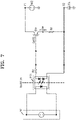
- FIG. 1 illustrates the configuration of a device for controlling a pre-charge current generated when electrically connecting a first terminal P1 and a second terminal P2 according to an embodiment of the present disclosure.
- the device for controlling a pre-charge current may include the first terminal P1, the second terminal P2, a switch SW, a first transistor TR1, a second transistor TR2, a first resistor R1, a second resistor R2, a third resistor R3, a capacitor C, a photocoupler PT1, and a first power source W1.
- the first terminal P1 and the second terminal P2 may be connected to two devices to be electrically connected to each other, respectively.
- a second power source may be electrically connected to the first terminal P1
- a load driven by the second power source connected to the first terminal P1 may be electrically connected to the second terminal P2.
- the second power source connected to the first terminal P1 may be a high-voltage battery for driving an electric vehicle, for example
- the load connected to the second terminal P2 may be a motor for driving the electric vehicle, for example.
- the load connected to the second terminal P2 may include a capacitive component and/or an inductive component for generating the pre-charge current.
- pre-charge may refer to a phenomenon in which energy is momentarily supplied to a device in connection between two devices due to the capacitive and/or inductive component of the device.
- a phenomenon in which, when connecting a power source (for example, the above-described second power source) to a load (for example, the above-described motor), energy is momentarily supplied to the load may correspond to this pre-charge phenomenon. This phenomenon frequently occurs in the initial connection between two devices, which results in serious damage to the device with a momentary pre-charge current accompanied.
- FIG. 2 is a view illustrating an aspect of a general pre-charge current.
- a large pre-charge current Ipr accompanied by the pre-charge phenomenon momentarily occurs at an initial connection time point t0 of two devices (for example, a power source and a load), and then the pre-charge current Ipr decreases exponentially.
- the pre-charge current Ipr that momentarily occurs at the initial connection time point t0, as described above, is out of a maximum current tolerance of the device (for example, the load), which may result in serious damage to the device and stress.
- the present disclosure prevents serious damage to the device by properly controlling the pre-charge current Ipr, minimizes the stress of elements constituting the device, and further prevents the use of expensive elements in preparation for the pre-charge in design and manufacture of the device. A detailed description thereof will be provided later.
- a switch SW may control the magnitude of a current flowing between the first terminal P1 and the second terminal P2 described above based on a GATE voltage of the switch SW or may interrupt electrical connection between the first terminal P1 and the second terminal P2. For example, the switch SW may increase the magnitude of the current flowing through the switch SW in proportion to the GATE voltage of the switch SW.
- the switch SW may be positioned on a line for electrically connecting the first terminal P1 and the second terminal P2. In other words, if the switch SW is on a line electrically connecting the first terminal P1 and the second terminal P2, the switch SW may be arranged regardless of a relative position with other components.
- the switch SW may be one of a field effect transistor (FET), a bipolar junction transistor (BJT), and an insulated gate bipolar mode transistor (IGBT).
- FET field effect transistor
- BJT bipolar junction transistor
- IGBT insulated gate bipolar mode transistor
- this is just an example, and the present disclosure is not limited thereto, and any element capable of controlling the magnitude of a current flowing through itself according to an input voltage to GATE may be used as the switch SW of the present disclosure without limitation.
- the first transistor TR1 may limit the magnitude of a pre-charge current on a line when the BASE voltage generated by the first resistor R1 is equal to or greater than a predetermined threshold voltage.
- the first transistor TR1 may be turned on when a BASE voltage generated by the first resistor R1 is equal to or greater than the predetermined threshold voltage, thereby decreasing a GATE voltage of the switch SW and thus the magnitude of a current flowing through the switch SW may be decreased and the magnitude of the pre-charge current may be limited.
- the first resistor R1 described above may be arranged on the line for electrically connecting the first terminal P1 and the second terminal P2, and a detailed description thereof will be provided later.
- the second transistor TR2 may decrease the amount of a current flowing through the second transistor TR2 so that a BASE voltage of the second transistor T2 may be increased.
- a BASE voltage of the second transistor TR2 may be relatively low.
- the GATE voltage of the switch SW at that time point may be decreased to a level similar to a reference potential GND. A detailed description thereof will be provided later.
- the second transistor TR2 may decrease a current flowing through the second transistor TR2 as the capacitor C is charged, thereby increasing the GATE voltage of the switch SW.
- the second transistor TR2 may linearly increase the GATE voltage of the switch WS so that the pre-charge current may be linearly increased.
- the first transistor TR1 and the second transistor TR2 described above may be one of an FET, a BJT, and an IGBT.
- this is just an example, and the present disclosure is not limited thereto.
- the first resistor R1 may be arranged on the line for electrically connecting the first terminal P1 and the second terminal P2 so as to generate the BASE voltage of the first transistor TR1 that limits the magnitude of the pre-charge current on the line.
- the second resistor R2 may control an operating time of the second transistor TR2 along with the capacitor C.
- the second transistor TR2 may decrease the current flowing through the second transistor TR2 as the capacitor C is charged, thereby increasing the GATE voltage of the switch SW.
- the operating time of the second transistor TR2 may refer to a time required to decrease the current flowing through the second transistor TR2 to be equal to or less than a predetermined amount, i.e., a time required until the second transistor TR2 is turned off.
- a predetermined amount i.e., a time required until the second transistor TR2 is turned off.
- the pre-charge current may be gently increased, and as the operating time decreases, the pre-charge current may be steeply increased.
- a third resistor R3 is for preventing a short circuit and may electrically connect the photocoupler PT1 to be described later, to the second resistor R2.
- the capacitor C according to an embodiment of the present disclosure may be charged by power supplied by the photocoupler PT1 to be described later, so that the pre-charge current may be gradually increased.
- the charging voltage of the capacitor C described above may generate the BASE voltage of the second transistor TR2.
- the GATE voltage of the switch SW may be changed by the BASE voltage of the second transistor TR2.
- the pre-charge current may be gradually increased according to charging of the capacitor C.
- the capacitor C may control the operating time of the second transistor TR2 along with the second resistor R2 described above. Because a description thereof has been provided above, it will be omitted.
- the photocoupler PT1 may receive, in a state insulated from the first power source W1, an optical signal from the first power source W1 and may supply power.
- the photocoupler PT1 may convert power supplied by the first power source W1 into an optical signal and may receive the optical signal again so that a right circuit may receive power in a state in which a circuit formed by the first power source W1 and a circuit for receiving power are insulated from each other.
- the first power source W1 may be a circuit different from the second power source connected to the first terminal P1 described above.
- the first power source W1 may be a battery provided for starting a vehicle or driving electronic equipment
- the second power source may be a battery provided for driving the vehicle, i.e., driving the vehicle.
- this is just an example, and the present disclosure is not limited thereto.
- FIG. 3 is a view illustrating an aspect of a pre-charge current controlled by a pre-charge current control device according to an embodiment of the present disclosure.
- the pre-charge current controlled by the pre-charge current control device is not steeply increased.
- a time period T1 in which the current does not flow (or a time period in which the current flows finely)
- a time period T3 in which the current is maintained at a constant level and a time period T4 in which the current decreases, may be provided.
- FIG. 4 is a view for explaining an operation of the pre-charge current control device at a time point t0 of FIG. 3 .
- the supply of power by the first power source W1 starts from the time point t0.
- the photocoupler PT1 may receive an optical signal from the first power source W1 to supply power to the right circuit of the device. Charging of the capacitor C may start due to a current I1 generated by power supplied by the photocoupler PT1.
- a predetermined voltage may be applied to the GATE of the switch SW due to the power supplied by the photocoupler PT1.
- a fine current I2 may flow between the first terminal P1 and the second terminal P2.
- the fine current I2 may be gradually increased.
- a BASE voltage of the first transistor TR1 may be increased to a predetermined threshold voltage by the first resistor R1.
- FIG. 5 is a view for explaining an operation of the current control device when the BASE voltage of the first transistor TR1 is increased to a predetermined threshold voltage in a time period T1.
- the first transistor TR1 may decrease the GATE voltage of the switch SW and may limit the magnitude of the pre-charge current Ipr.
- the first transistor TR1 may be turned on when the BASE voltage generated by the first resistor R1 is equal to or greater than the predetermined threshold voltage, so that a path such as CP1 may be generated.
- the GATE voltage of the switch SW may be decreased to a level similar to the reference potential GND.
- the switch SW may limit the pre-charge current Ipr between the first terminal P1 and the second terminal P2, as in the time period T1 of FIG. 3 .
- FIG. 6 is a view for explaining an operation of the current control device when a BASE voltage of a second transistor TR2 is gradually increased in a time period T2 and a time period T3.
- the GATE voltage of the switch SW may be decreased to the level similar to the reference potential GND through the path such as CP1 of FIG. 5 at the time point t1 (i.e., in the time period T1).
- the BASE voltage of the second transistor TR2 may be increased based on the charging voltage of the capacitor C.
- the second transistor TR2 may decrease the current flowing through the second transistor TR2 as the BASE voltage increases.
- the GATE voltage of the switch SW may be increased.
- the second transistor TR2 may linearly increase the GATE voltage of the switch SW so that the pre-charge current Ipr may be linearly increased, as in the time period T2 of FIG. 3 .
- the pre-charge current Ipr may be limited to a predetermined value, as in the time period T3 of FIG. 3 , according to a voltage generated by the photocoupler PT1.
- FIG. 7 is a view illustrating an equivalent circuit of the pre-charge current control device when a pre-charge current is gradually decreased in a time period T4.
- the pre-charge current may refer to a phenomenon in which energy is momentarily supplied to a device due to the capacitive load CL connected to the device. Thus, the amount of the pre-charge current is limited, and the pre-charge current may momentarily occur only in the initial connection between two devices.
- the pre-charge current may be decreased, as in the time period T4 of FIG. 3 , when charging of the capacitive load CL connected to the device is completed.
- the GATE voltage of the switch SW may be maintained at a predetermined voltage by power supplied by the photocoupler PT1.
- the switch SW may maintain the short-circuit state of the first terminal P1 and the second terminal P2 due to the GATE voltage maintained at the predetermined voltage.
- the present disclosure may prevent a momentarily excessive current from being supplied to a device, so that the failure of the device or an increase in the fatigue of elements constituting the device may be prevented.
- the present disclosure may prevent the generation of high momentary power generated by a pre-charge current so that the need for the use of high-cost devices in the manufacture and design of a device may be reduced.
Description
- The present disclosure relates to a pre-charge current control device.
- Today, battery pack-related technologies are being developed with the development of electric vehicles and energy storage technology, and these battery packs are generally designed with high voltage and capacity so as to drive a device.
- In the initial connection between the battery pack and the device, a pre-charge phenomenon frequently occurs due to inductive and/or capacitive elements of the device. As the voltage and capacity of a battery increase, as described above, a large pre-charge phenomenon occurs.
- According to the prior art, in order to prepare for this pre-charge phenomenon, a device is designed by using elements capable of withstanding high current or high voltage. Accordingly, there is a problem in that the manufacturing cost of the device increases.
- In addition, the stress of each element of the device has increased by the pre-charge phenomenon, and thus, this may result in serious damage to the device.
-
US 2008258551 A1 discloses an electronic dimming ballast comprising a control circuit, which is coupled to a digital communication link via a communication circuit. The communication circuit comprises a receiving circuit for detecting when the digital ballast communication link is shorted and for providing a received digital message to the control circuit. The communication circuit also comprises a transmitting circuit for shorting the communication link in response to the control circuit. The communication circuit also includes a high-voltage fault protection circuit for protecting the circuitry of the communication circuit if the communication circuit high-voltage mains voltages. -
JP 5030901 B2 - Provided are embodiments of the present disclosure in which momentarily excessive current may be prevented from being supplied to a device, so that the failure of the device or an increase in the fatigue of elements constituting the device may be prevented.
- Provided are also embodiments of the present disclosure in which the generation of high momentary power generated by a pre-charge current may be prevented so that the need for the use of high-cost devices in the manufacture and design of a device may be reduced.
- According to an aspect, there is provided a device for controlling a pre-charge current generated when electrically connected a first terminal and a second terminal, as set out in claim 1. Optional features are set out in the dependent claims.
- According to various embodiments of the present disclosure, momentarily excessive current can be prevented from being supplied to a device, so that the failure of the device or an increase in the fatigue of elements constituting the device may be prevented.
- In addition, the generation of high momentary power generated by a pre-charge current can be prevented so that the need for the use of high-cost devices in the manufacture and design of a device can be reduced.
-
-
FIG. 1 illustrates a configuration of a device for controlling a pre-charge current generated when electrically connecting a first terminal and a second terminal, according to an embodiment of the present disclosure. -
FIG. 2 is a view illustrating an aspect of a general pre-charge current. -
FIG. 3 is a view illustrating an aspect of a pre-charge current controlled by a pre-charge current control device according to an embodiment of the present disclosure. -
FIG. 4 is a view for explaining an operation of a pre-charge current control device at a time point t0 ofFIG. 3 . -
FIG. 5 is a view for explaining an operation of the current control device when a BASE voltage of a first transistor is increased to a predetermined threshold voltage in a time period T1. -
FIG. 6 is a view for explaining an operation of the current control device when a BASE voltage of a second transistor is gradually increased in a time period T2 and a time period T3. -
FIG. 7 is a view illustrating an equivalent circuit of the pre-charge current control device when a pre-charge current is gradually decreased in a time period T4. - A device for controlling a pre-charge current generated when electrically connecting a first terminal and a second terminal includes a switch for controlling a magnitude of a current flowing between the first terminal and the second terminal, a first resistor for generating a base voltage of a first transistor in proportion to a magnitude of the pre-charge current flowing between the first terminal and the second terminal, the first transistor for limiting the magnitude of the pre-charge current when a voltage generated by the first resistor is equal to or greater than a predetermined threshold voltage, a photocoupler for receiving, in a state insulated from a first power source, an optical signal from the first power source and supplying power, a capacitor charged by the power supplied by the photocoupler, a second transistor for controlling the magnitude of the pre-charge current on the basis of a charging voltage of the capacitor, and a second resistor for controlling an operating time of the second transistor along with the capacitor.
- Advantages and features of the present disclosure, and ways to achieve them will become apparent by referring to embodiments that will be described later in detail with reference to the drawings. However, the present disclosure is not limited to embodiments presented below but may be embodied in various different forms, and it is to be appreciated that all changes, equivalents, and substitutes that do not depart from the scope of the claims are encompassed. The embodiments presented below are provided to make the disclosure of the present disclosure complete, and to fully inform the scope of the present disclosure to those skilled in the art to which the present disclosure pertains. In the description of the present disclosure, certain detailed explanations of related art are omitted when it is deemed that they may unnecessarily obscure the essence of the present disclosure.
- For example, specific shapes, structures, and characteristics described in the present specification may be implemented by changing from one embodiment to another embodiment without departing from the scope of the present disclosure, which is defined by the appended claims. In addition, it should be understood that the position or arrangement of individual components within each embodiment may be changed without departing from scope of the present disclosure, which is defined by the appended claims. Therefore, the following detailed description is not intended to be done in a limiting sense, and the scope of the present disclosure should be taken to cover the scope claimed by the claims. Similar reference numerals in the drawings represent the same or similar components throughout several aspects. In other words, specific details described are simple examples. Specific implementations can vary from these exemplary details and can still be considered within the scope of the present disclosure, which is defined by the appended claims.
- It will be understood that although the terms "first," "second," etc. may be used herein to describe various components, these components should not be limited by these terms. The terms are used only to distinguish one component from other components.
- The terms used in this application are only used to describe specific embodiments, and are not intended to limit the present disclosure. As used herein, the singular forms "a," "an," and the" are intended to include the plural forms as well, unless the context clearly indicates otherwise. It will be further understood that the terms "comprises" and/or "comprising" used herein specify the presence of stated features or components, but do not preclude the presence or addition of one or more other features or components. It will be understood that although the terms "first," "second," etc. may be used herein to describe various components, these components should not be limited by these terms. These terms are used only to distinguish one component from other components.
- Hereinafter, embodiments of the present disclosure will be described below in more detail with reference to the accompanying drawings. Those components that are the same or are in correspondence are rendered the same reference numeral regardless of the figure number, and a redundant description therewith is omitted.
-
FIG. 1 illustrates the configuration of a device for controlling a pre-charge current generated when electrically connecting a first terminal P1 and a second terminal P2 according to an embodiment of the present disclosure. - Referring to
FIG. 1 , the device for controlling a pre-charge current according to an embodiment of the present disclosure may include the first terminal P1, the second terminal P2, a switch SW, a first transistor TR1, a second transistor TR2, a first resistor R1, a second resistor R2, a third resistor R3, a capacitor C, a photocoupler PT1, and a first power source W1. - The first terminal P1 and the second terminal P2 according to an embodiment of the present disclosure may be connected to two devices to be electrically connected to each other, respectively. For example, a second power source may be electrically connected to the first terminal P1, and a load driven by the second power source connected to the first terminal P1 may be electrically connected to the second terminal P2. In this case, the second power source connected to the first terminal P1 may be a high-voltage battery for driving an electric vehicle, for example, and the load connected to the second terminal P2 may be a motor for driving the electric vehicle, for example.
- Moreover, the load connected to the second terminal P2 may include a capacitive component and/or an inductive component for generating the pre-charge current. In this case, pre-charge may refer to a phenomenon in which energy is momentarily supplied to a device in connection between two devices due to the capacitive and/or inductive component of the device. For example, a phenomenon in which, when connecting a power source (for example, the above-described second power source) to a load (for example, the above-described motor), energy is momentarily supplied to the load, may correspond to this pre-charge phenomenon. This phenomenon frequently occurs in the initial connection between two devices, which results in serious damage to the device with a momentary pre-charge current accompanied.
-
FIG. 2 is a view illustrating an aspect of a general pre-charge current. - Referring to
FIG. 2 , a large pre-charge current Ipr accompanied by the pre-charge phenomenon momentarily occurs at an initial connection time point t0 of two devices (for example, a power source and a load), and then the pre-charge current Ipr decreases exponentially. - The pre-charge current Ipr that momentarily occurs at the initial connection time point t0, as described above, is out of a maximum current tolerance of the device (for example, the load), which may result in serious damage to the device and stress.
- The present disclosure prevents serious damage to the device by properly controlling the pre-charge current Ipr, minimizes the stress of elements constituting the device, and further prevents the use of expensive elements in preparation for the pre-charge in design and manufacture of the device. A detailed description thereof will be provided later.
- A switch SW according to an embodiment of the present disclosure may control the magnitude of a current flowing between the first terminal P1 and the second terminal P2 described above based on a GATE voltage of the switch SW or may interrupt electrical connection between the first terminal P1 and the second terminal P2. For example, the switch SW may increase the magnitude of the current flowing through the switch SW in proportion to the GATE voltage of the switch SW.
- To this end, the switch SW may be positioned on a line for electrically connecting the first terminal P1 and the second terminal P2. In other words, if the switch SW is on a line electrically connecting the first terminal P1 and the second terminal P2, the switch SW may be arranged regardless of a relative position with other components.
- The switch SW according to an embodiment of the present disclosure may be one of a field effect transistor (FET), a bipolar junction transistor (BJT), and an insulated gate bipolar mode transistor (IGBT). However, this is just an example, and the present disclosure is not limited thereto, and any element capable of controlling the magnitude of a current flowing through itself according to an input voltage to GATE may be used as the switch SW of the present disclosure without limitation.
- The first transistor TR1 according to an embodiment of the present disclosure may limit the magnitude of a pre-charge current on a line when the BASE voltage generated by the first resistor R1 is equal to or greater than a predetermined threshold voltage. In other words, the first transistor TR1 may be turned on when a BASE voltage generated by the first resistor R1 is equal to or greater than the predetermined threshold voltage, thereby decreasing a GATE voltage of the switch SW and thus the magnitude of a current flowing through the switch SW may be decreased and the magnitude of the pre-charge current may be limited. Moreover, the first resistor R1 described above may be arranged on the line for electrically connecting the first terminal P1 and the second terminal P2, and a detailed description thereof will be provided later.
- On the other hand, the second transistor TR2 that will be described later may decrease the amount of a current flowing through the second transistor TR2 so that a BASE voltage of the second transistor T2 may be increased. Thus, at a time point when the first transistor TR1 is turned on, a BASE voltage of the second transistor TR2 may be relatively low. Thus, the GATE voltage of the switch SW at that time point may be decreased to a level similar to a reference potential GND. A detailed description thereof will be provided later.
- The second transistor TR2 according to an embodiment of the present disclosure may control the magnitude of the pre-charge current between the first terminal P1 and the second terminal P2 based on a charging voltage of a capacitor C that will be described later. In more detail, the charging voltage of the capacitor C may be gradually increased by the first power source W1 according to an operation of the pre-charge current control device, and the charging voltage of the capacitor C may generate a BASE voltage of the second transistor TR2.
- As described above, the second transistor TR2 may decrease a current flowing through the second transistor TR2 as the capacitor C is charged, thereby increasing the GATE voltage of the switch SW. In this case, the second transistor TR2 may linearly increase the GATE voltage of the switch WS so that the pre-charge current may be linearly increased.
- Moreover, despite their names, the first transistor TR1 and the second transistor TR2 described above may be one of an FET, a BJT, and an IGBT. However, this is just an example, and the present disclosure is not limited thereto.
- The first resistor R1 according to an embodiment of the present disclosure may be arranged on the line for electrically connecting the first terminal P1 and the second terminal P2 so as to generate the BASE voltage of the first transistor TR1 that limits the magnitude of the pre-charge current on the line.
- The second resistor R2 according to an embodiment of the present disclosure may control an operating time of the second transistor TR2 along with the capacitor C. In this case, the second transistor TR2 may decrease the current flowing through the second transistor TR2 as the capacitor C is charged, thereby increasing the GATE voltage of the switch SW.
- Thus, in the present disclosure, the operating time of the second transistor TR2 may refer to a time required to decrease the current flowing through the second transistor TR2 to be equal to or less than a predetermined amount, i.e., a time required until the second transistor TR2 is turned off. As the operating time increases, the pre-charge current may be gently increased, and as the operating time decreases, the pre-charge current may be steeply increased.
- A third resistor R3 according to an embodiment of the present disclosure is for preventing a short circuit and may electrically connect the photocoupler PT1 to be described later, to the second resistor R2.
- The capacitor C according to an embodiment of the present disclosure may be charged by power supplied by the photocoupler PT1 to be described later, so that the pre-charge current may be gradually increased. The charging voltage of the capacitor C described above may generate the BASE voltage of the second transistor TR2. In addition, the GATE voltage of the switch SW may be changed by the BASE voltage of the second transistor TR2. Thus, the pre-charge current may be gradually increased according to charging of the capacitor C.
- Moreover, the capacitor C may control the operating time of the second transistor TR2 along with the second resistor R2 described above. Because a description thereof has been provided above, it will be omitted.
- The photocoupler PT1 according to an embodiment of the present disclosure may receive, in a state insulated from the first power source W1, an optical signal from the first power source W1 and may supply power. In more detail, the photocoupler PT1 may convert power supplied by the first power source W1 into an optical signal and may receive the optical signal again so that a right circuit may receive power in a state in which a circuit formed by the first power source W1 and a circuit for receiving power are insulated from each other.
- Moreover, the first power source W1 may be a circuit different from the second power source connected to the first terminal P1 described above. For example, when the pre-charge current control device according to an embodiment of the present disclosure is provided in an electric vehicle, the first power source W1 may be a battery provided for starting a vehicle or driving electronic equipment, and the second power source may be a battery provided for driving the vehicle, i.e., driving the vehicle. However, this is just an example, and the present disclosure is not limited thereto.
- Hereinafter, an operation according to the passage of time of the pre-charge current control device according to an embodiment of the present disclosure will be described with reference to
FIGS. 3 through 7 . In addition, it is assumed that the second power source W2 is connected to the first terminal P1 and a capacitive load CL is connected to the second terminal P2 of the pre-charge current control device according to an embodiment of the present disclosure. -
FIG. 3 is a view illustrating an aspect of a pre-charge current controlled by a pre-charge current control device according to an embodiment of the present disclosure. - Compared to
FIG. 2 , the pre-charge current controlled by the pre-charge current control device according to an embodiment of the present disclosure is not steeply increased. In addition, when checking the magnitude of the current over time, a time period T1 in which the current does not flow (or a time period in which the current flows finely), a time period T2 in which the current linearly increases, a time period T3 in which the current is maintained at a constant level, and a time period T4 in which the current decreases, may be provided. - Hereinafter, the operation of the pre-charge current control device in each of time periods T1 through T4 or at a certain time point t0 will be mainly described.
-
FIG. 4 is a view for explaining an operation of the pre-charge current control device at a time point t0 ofFIG. 3 . For convenience of explanation, it is assumed that the supply of power by the first power source W1 starts from the time point t0. - Under the assumptions described above, the photocoupler PT1 may receive an optical signal from the first power source W1 to supply power to the right circuit of the device. Charging of the capacitor C may start due to a current I1 generated by power supplied by the photocoupler PT1.
- A predetermined voltage may be applied to the GATE of the switch SW due to the power supplied by the photocoupler PT1. Thus, a fine current I2 may flow between the first terminal P1 and the second terminal P2.
- After the time point t0, as the voltage applied to the GATE of the switch SW is increased, the fine current I2 may be gradually increased. Thus, a BASE voltage of the first transistor TR1 may be increased to a predetermined threshold voltage by the first resistor R1.
-
FIG. 5 is a view for explaining an operation of the current control device when the BASE voltage of the first transistor TR1 is increased to a predetermined threshold voltage in a time period T1. - When a current (see I2 of
FIG. 4 ) flowing through the first resistor R1 increases according to the process described with respect toFIG. 4 and thus the BASE voltage of the first transistor TR1 is equal to or greater than a predetermined threshold voltage, the first transistor TR1 may decrease the GATE voltage of the switch SW and may limit the magnitude of the pre-charge current Ipr. - In other words, the first transistor TR1 may be turned on when the BASE voltage generated by the first resistor R1 is equal to or greater than the predetermined threshold voltage, so that a path such as CP1 may be generated. Thus, the GATE voltage of the switch SW may be decreased to a level similar to the reference potential GND.
- When the GATE voltage of the switch SW is decreased to the level similar to the reference potential GND, the switch SW may limit the pre-charge current Ipr between the first terminal P1 and the second terminal P2, as in the time period T1 of
FIG. 3 . -
FIG. 6 is a view for explaining an operation of the current control device when a BASE voltage of a second transistor TR2 is gradually increased in a time period T2 and a time period T3. - As described with respect to
FIG. 5 , the GATE voltage of the switch SW may be decreased to the level similar to the reference potential GND through the path such as CP1 ofFIG. 5 at the time point t1 (i.e., in the time period T1). - After the time point t1, the BASE voltage of the second transistor TR2 may be increased based on the charging voltage of the capacitor C. The second transistor TR2 may decrease the current flowing through the second transistor TR2 as the BASE voltage increases. Thus, the GATE voltage of the switch SW may be increased.
- In this case, the second transistor TR2 may linearly increase the GATE voltage of the switch SW so that the pre-charge current Ipr may be linearly increased, as in the time period T2 of
FIG. 3 . - Moreover, the pre-charge current Ipr may be limited to a predetermined value, as in the time period T3 of
FIG. 3 , according to a voltage generated by the photocoupler PT1. -
FIG. 7 is a view illustrating an equivalent circuit of the pre-charge current control device when a pre-charge current is gradually decreased in a time period T4. - The pre-charge current may refer to a phenomenon in which energy is momentarily supplied to a device due to the capacitive load CL connected to the device. Thus, the amount of the pre-charge current is limited, and the pre-charge current may momentarily occur only in the initial connection between two devices.
- The pre-charge current may be decreased, as in the time period T4 of
FIG. 3 , when charging of the capacitive load CL connected to the device is completed. In this case, the GATE voltage of the switch SW may be maintained at a predetermined voltage by power supplied by the photocoupler PT1. In addition, the switch SW may maintain the short-circuit state of the first terminal P1 and the second terminal P2 due to the GATE voltage maintained at the predetermined voltage. - In this way, the present disclosure may prevent a momentarily excessive current from being supplied to a device, so that the failure of the device or an increase in the fatigue of elements constituting the device may be prevented.
- The present disclosure may prevent the generation of high momentary power generated by a pre-charge current so that the need for the use of high-cost devices in the manufacture and design of a device may be reduced.
- The present disclosure has been particularly shown and described with reference to exemplary embodiments thereof. It will be understood by those skilled in the art that various changes in form and details may be made therein without departing from the scope of the invention as defined by the appended claims. The exemplary embodiments should be considered in descriptive sense only and not for purposes of limitation. Therefore, the scope of the invention is defined not by the detailed description of the invention but by the appended claims, and all differences within the scope will be construed as being included in the present invention.
Claims (8)
- A device for controlling a pre-charge current generated when electrically connecting a first terminal (P1) and a second terminal (P2), the device comprising:a switch (SW) for controlling a magnitude of a current flowing between the first terminal (P1) and the second terminal (P2);a first resistor (R1) for generating a base voltage of a first transistor (TR1) in proportion to a magnitude of the pre-charge current flowing between the first terminal (P1) and the second terminal (P2);the first transistor (TR1) for limiting the magnitude of the pre-charge current when a voltage generated by the first resistor (R1) is equal to or greater than a predetermined threshold voltage;a photocoupler (PT1) for receiving, in a state insulated from a first power source (W1), an optical signal from the first power source (W1) and supplying power;a capacitor (C) for being charged by the power supplied by the photocoupler (PT1);a second transistor (TR2) for controlling the magnitude of the pre-charge current on a basis of a charging voltage of the capacitor (C), wherein the charging voltage of the capacitor (C) generates a base voltage of the second transistor (TR2), and as the capacitor (C) is charged by the power supplied by the photocoupler (PT1), the second transistor (TR2) is configured to decrease a current flowing through the second transistor (TR2) so as to increase a gate voltage of the switch (SW); anda second resistor (R2) for controlling an operating time of the second transistor (TR2) along with the capacitor (C).
- The device of claim 1, wherein the second transistor (TR2) is configured to decrease the current flowing through the second transistor (TR2) so as to linearly increase the gate voltage of the switch (SW).
- The device of claim 1, wherein the switch (SW) is configured to increase a magnitude of a current flowing through the switch (SW) in proportion to a gate voltage of the switch (SW).
- The device of claim 1, wherein, when the voltage generated by the first resistor (R1) is equal to or greater than a predetermined threshold voltage,
the first transistor (TR1) decreases a gate voltage of the switch (SW) so as to limit the magnitude of the pre-charge current. - The device of claim 1, further comprising a third resistor (R3) for preventing a short circuit,
wherein the third resistor (R3) electrically connects the photocoupler (PT1) and the second resistor (R2). - The device of claim 1, wherein a second power source is electrically connected to the first terminal (P1), and
a load is electrically connected to the second terminal (P2). - The device of claim 6, wherein the load comprises a capacitive element for generating the pre-charge current.
- The device of claim 5, wherein, when charging of the capacitive element is completed, the pre-charge current is decreased, andwhen charging of the capacitive element is completed, the gate voltage of the switch (SW) is maintained at a predetermined voltage by the power supplied by the photocoupler (PT1), andthe switch (SW) is configured to maintain a short-circuit state of the first terminal (P1) and the second terminal (P2) by the gate voltage maintained at the predetermined voltage.
Priority Applications (1)
| Application Number | Priority Date | Filing Date | Title |
|---|---|---|---|
| HUE18898529A HUE059659T2 (en) | 2018-01-03 | 2018-01-03 | Pre-charge current control device |
Applications Claiming Priority (1)
| Application Number | Priority Date | Filing Date | Title |
|---|---|---|---|
| PCT/KR2018/000070 WO2019135417A1 (en) | 2018-01-03 | 2018-01-03 | Pre-charge current control device |
Publications (3)
| Publication Number | Publication Date |
|---|---|
| EP3719954A4 EP3719954A4 (en) | 2020-10-07 |
| EP3719954A1 EP3719954A1 (en) | 2020-10-07 |
| EP3719954B1 true EP3719954B1 (en) | 2022-08-10 |
Family
ID=67143753
Family Applications (1)
| Application Number | Title | Priority Date | Filing Date |
|---|---|---|---|
| EP18898529.5A Active EP3719954B1 (en) | 2018-01-03 | 2018-01-03 | Pre-charge current control device |
Country Status (8)
| Country | Link |
|---|---|
| US (1) | US11824397B2 (en) |
| EP (1) | EP3719954B1 (en) |
| KR (1) | KR102533158B1 (en) |
| CN (1) | CN111712986B (en) |
| HU (1) | HUE059659T2 (en) |
| PL (1) | PL3719954T3 (en) |
| TW (1) | TWI688184B (en) |
| WO (1) | WO2019135417A1 (en) |
Families Citing this family (1)
| Publication number | Priority date | Publication date | Assignee | Title |
|---|---|---|---|---|
| CN110429698B (en) * | 2019-09-29 | 2020-01-31 | 珠海格力电器股份有限公司 | self-adaptive charging circuit and control method thereof |
Family Cites Families (26)
| Publication number | Priority date | Publication date | Assignee | Title |
|---|---|---|---|---|
| JP2004048888A (en) * | 2002-07-10 | 2004-02-12 | Fujitsu Ltd | Rush current preventive circuit |
| US8203810B2 (en) | 2006-04-04 | 2012-06-19 | Tyco Electronics Corporation | Solid state pre-charge module |
| BRPI0709767A2 (en) * | 2006-04-04 | 2011-07-26 | Tyco Eletronics Corp | solid state preload module |
| US7764479B2 (en) | 2007-04-18 | 2010-07-27 | Lutron Electronics Co., Inc. | Communication circuit for a digital electronic dimming ballast |
| JP4431996B2 (en) | 2007-07-09 | 2010-03-17 | Smc株式会社 | Solenoid valve drive circuit and solenoid valve |
| CN101645609B (en) | 2008-08-08 | 2012-07-04 | 凹凸电子(武汉)有限公司 | Battery system, charging/discharging circuit thereof and charging/discharging control method thereof |
| US8164309B2 (en) | 2008-08-08 | 2012-04-24 | O2Micro, Inc | Battery charging system with trickle charging/discharging control |
| JP5030901B2 (en) * | 2008-08-29 | 2012-09-19 | 株式会社藤商事 | Game machine |
| CN201601506U (en) | 2009-11-16 | 2010-10-06 | 深圳市五洲龙汽车有限公司 | Photoelectric isolation non-contact quick pre-charging circuit |
| CN102983607A (en) * | 2012-12-12 | 2013-03-20 | 奇瑞汽车股份有限公司 | Precharge device for motor controller of electromobile |
| WO2015001374A1 (en) | 2013-07-04 | 2015-01-08 | Freescale Semiconductor, Inc. | A gate drive circuit and a method for controlling a power transistor |
| KR101457986B1 (en) | 2013-08-09 | 2014-11-10 | 주식회사 아이티엠반도체 | Battery pack overcharge protection circuit |
| KR102080635B1 (en) | 2013-10-15 | 2020-02-24 | 현대모비스 주식회사 | All-in-one electronic relay, Power source control apparatus using the same, and Method for operating pre-charge function using the apparatus |
| KR20150050858A (en) | 2013-11-01 | 2015-05-11 | 현대모비스 주식회사 | Pre-charge electronic relay, Power source control apparatus using the same, and Method for operating pre-charge function using the apparatus |
| KR20150061447A (en) | 2013-11-27 | 2015-06-04 | 한국단자공업 주식회사 | Smart Solid State Relay based on Electric Vehicle |
| US9214888B2 (en) | 2013-12-20 | 2015-12-15 | Lg Chem, Ltd. | Pre-charging system for a capacitor in a voltage inverter for an electric motor |
| US9673617B2 (en) | 2014-02-11 | 2017-06-06 | Te Connectivity Corporation | Pre-charge circuit for an electromechanical relay |
| US9800069B2 (en) | 2014-04-03 | 2017-10-24 | Ford Global Technologies, Llc | Linear current regulator for high voltage bus precharging |
| KR101787639B1 (en) | 2015-02-24 | 2017-10-18 | 주식회사 엘지화학 | Battery apparatus |
| CN106611986A (en) | 2015-10-26 | 2017-05-03 | 通用电气公司 | System and method for pre-charging capacitor bank |
| US9954353B2 (en) | 2015-11-05 | 2018-04-24 | GM Global Technology Operations LLC | Self turn-on and turn-off pre-charge circuit to limit bulk capacitor inrush current |
| US10076964B2 (en) * | 2015-12-15 | 2018-09-18 | Faraday & Future Inc. | Pre-charge system and method |
| CN107276378B (en) * | 2016-04-08 | 2019-03-15 | 台达电子企业管理(上海)有限公司 | Precharge control method |
| CN205693367U (en) * | 2016-06-17 | 2016-11-16 | 广州开能电气实业有限公司 | A kind of capacitor pre-charge circuit |
| CN106274528B (en) * | 2016-08-26 | 2018-08-28 | 朱利东 | Pre-charge circuit with automatic control function and method |
| CN108270250A (en) | 2016-12-30 | 2018-07-10 | 群光电能科技股份有限公司 | Charging system |
-
2018
- 2018-01-03 CN CN201880089471.0A patent/CN111712986B/en active Active
- 2018-01-03 US US16/960,173 patent/US11824397B2/en active Active
- 2018-01-03 HU HUE18898529A patent/HUE059659T2/en unknown
- 2018-01-03 EP EP18898529.5A patent/EP3719954B1/en active Active
- 2018-01-03 KR KR1020207014776A patent/KR102533158B1/en not_active Application Discontinuation
- 2018-01-03 WO PCT/KR2018/000070 patent/WO2019135417A1/en unknown
- 2018-01-03 PL PL18898529.5T patent/PL3719954T3/en unknown
- 2018-12-26 TW TW107147138A patent/TWI688184B/en active
Also Published As
| Publication number | Publication date |
|---|---|
| WO2019135417A1 (en) | 2019-07-11 |
| CN111712986B (en) | 2023-08-01 |
| PL3719954T3 (en) | 2022-09-26 |
| EP3719954A4 (en) | 2020-10-07 |
| TW201931715A (en) | 2019-08-01 |
| HUE059659T2 (en) | 2022-12-28 |
| TWI688184B (en) | 2020-03-11 |
| US11824397B2 (en) | 2023-11-21 |
| KR20200096510A (en) | 2020-08-12 |
| CN111712986A (en) | 2020-09-25 |
| KR102533158B1 (en) | 2023-05-17 |
| US20200358307A1 (en) | 2020-11-12 |
| EP3719954A1 (en) | 2020-10-07 |
Similar Documents
| Publication | Publication Date | Title |
|---|---|---|
| KR102285228B1 (en) | Secondary battery protection circuit, secondary battery protection device, battery pack and method of controlling secondary battery protection circuit | |
| KR101784740B1 (en) | Battery protection circuit and battery pack including same | |
| CN101752619A (en) | Rechargeable battery protection integrated circuit device, rechargeable battery protection module, and battery pack | |
| CN105144580A (en) | Semiconductor device | |
| EP3722142B1 (en) | Electric vehicle power relay assembly and driving method therefor | |
| CN111699603B (en) | Battery protection circuit and battery pack including the same | |
| KR102515881B1 (en) | Battery protection circuit and battery pack having same | |
| EP3719954B1 (en) | Pre-charge current control device | |
| US20100181968A1 (en) | Battery charger with overvoltage protection circuitry | |
| CN109155626B (en) | Power supply control device | |
| US10877102B2 (en) | Voltage detection device | |
| CN111656636B (en) | Power supply control device, power supply control method, and storage medium | |
| CN1063591C (en) | Power supply voltage supplying circuit | |
| US20070165341A1 (en) | Overvoltage-protective automotive power generation control circuit | |
| KR20080009895A (en) | Circuit for charging and discharging of smoothing capacitor | |
| CN216599036U (en) | Switching circuit, charging box and audio equipment | |
| WO2018066499A1 (en) | In-vehicle apparatus | |
| EP4152616A1 (en) | Relay drive circuit and battery system comprising same | |
| CN220291869U (en) | Driving circuit, battery management system and vehicle | |
| KR102555498B1 (en) | Inrush current limiter and system including the same | |
| CN216751227U (en) | Battery management circuit, battery management system and electric vehicle | |
| KR100303026B1 (en) | Integrated circuit for Feed-back voltage detection of a battery charger | |
| KR20230060481A (en) | Driving circuit of latche relay | |
| JPH0236734A (en) | Voltage controller for vehicle generator | |
| CN205377821U (en) | Switchgear |
Legal Events
| Date | Code | Title | Description |
|---|---|---|---|
| STAA | Information on the status of an ep patent application or granted ep patent |
Free format text: STATUS: THE INTERNATIONAL PUBLICATION HAS BEEN MADE |
|
| PUAI | Public reference made under article 153(3) epc to a published international application that has entered the european phase |
Free format text: ORIGINAL CODE: 0009012 |
|
| STAA | Information on the status of an ep patent application or granted ep patent |
Free format text: STATUS: REQUEST FOR EXAMINATION WAS MADE |
|
| 17P | Request for examination filed |
Effective date: 20200629 |
|
| A4 | Supplementary search report drawn up and despatched |
Effective date: 20200828 |
|
| AK | Designated contracting states |
Kind code of ref document: A1 Designated state(s): AL AT BE BG CH CY CZ DE DK EE ES FI FR GB GR HR HU IE IS IT LI LT LU LV MC MK MT NL NO PL PT RO RS SE SI SK SM TR |
|
| AX | Request for extension of the european patent |
Extension state: BA ME |
|
| RIN1 | Information on inventor provided before grant (corrected) |
Inventor name: JEON, PEEL SIK Inventor name: MOON, SOO DEOK Inventor name: PARK, KYUNG HOON |
|
| DAV | Request for validation of the european patent (deleted) | ||
| DAX | Request for extension of the european patent (deleted) | ||
| GRAP | Despatch of communication of intention to grant a patent |
Free format text: ORIGINAL CODE: EPIDOSNIGR1 |
|
| STAA | Information on the status of an ep patent application or granted ep patent |
Free format text: STATUS: GRANT OF PATENT IS INTENDED |
|
| INTG | Intention to grant announced |
Effective date: 20220325 |
|
| GRAS | Grant fee paid |
Free format text: ORIGINAL CODE: EPIDOSNIGR3 |
|
| GRAA | (expected) grant |
Free format text: ORIGINAL CODE: 0009210 |
|
| STAA | Information on the status of an ep patent application or granted ep patent |
Free format text: STATUS: THE PATENT HAS BEEN GRANTED |
|
| AK | Designated contracting states |
Kind code of ref document: B1 Designated state(s): AL AT BE BG CH CY CZ DE DK EE ES FI FR GB GR HR HU IE IS IT LI LT LU LV MC MK MT NL NO PL PT RO RS SE SI SK SM TR |
|
| REG | Reference to a national code |
Ref country code: AT Ref legal event code: REF Ref document number: 1511279 Country of ref document: AT Kind code of ref document: T Effective date: 20220815 Ref country code: CH Ref legal event code: EP |
|
| REG | Reference to a national code |
Ref country code: DE Ref legal event code: R096 Ref document number: 602018039271 Country of ref document: DE |
|
| REG | Reference to a national code |
Ref country code: IE Ref legal event code: FG4D |
|
| REG | Reference to a national code |
Ref country code: SE Ref legal event code: TRGR |
|
| REG | Reference to a national code |
Ref country code: NL Ref legal event code: MP Effective date: 20220810 |
|
| REG | Reference to a national code |
Ref country code: LT Ref legal event code: MG9D |
|
| REG | Reference to a national code |
Ref country code: HU Ref legal event code: AG4A Ref document number: E059659 Country of ref document: HU |
|
| PG25 | Lapsed in a contracting state [announced via postgrant information from national office to epo] |
Ref country code: RS Free format text: LAPSE BECAUSE OF FAILURE TO SUBMIT A TRANSLATION OF THE DESCRIPTION OR TO PAY THE FEE WITHIN THE PRESCRIBED TIME-LIMIT Effective date: 20220810 Ref country code: PT Free format text: LAPSE BECAUSE OF FAILURE TO SUBMIT A TRANSLATION OF THE DESCRIPTION OR TO PAY THE FEE WITHIN THE PRESCRIBED TIME-LIMIT Effective date: 20221212 Ref country code: NO Free format text: LAPSE BECAUSE OF FAILURE TO SUBMIT A TRANSLATION OF THE DESCRIPTION OR TO PAY THE FEE WITHIN THE PRESCRIBED TIME-LIMIT Effective date: 20221110 Ref country code: NL Free format text: LAPSE BECAUSE OF FAILURE TO SUBMIT A TRANSLATION OF THE DESCRIPTION OR TO PAY THE FEE WITHIN THE PRESCRIBED TIME-LIMIT Effective date: 20220810 Ref country code: LV Free format text: LAPSE BECAUSE OF FAILURE TO SUBMIT A TRANSLATION OF THE DESCRIPTION OR TO PAY THE FEE WITHIN THE PRESCRIBED TIME-LIMIT Effective date: 20220810 Ref country code: LT Free format text: LAPSE BECAUSE OF FAILURE TO SUBMIT A TRANSLATION OF THE DESCRIPTION OR TO PAY THE FEE WITHIN THE PRESCRIBED TIME-LIMIT Effective date: 20220810 Ref country code: FI Free format text: LAPSE BECAUSE OF FAILURE TO SUBMIT A TRANSLATION OF THE DESCRIPTION OR TO PAY THE FEE WITHIN THE PRESCRIBED TIME-LIMIT Effective date: 20220810 |
|
| PG25 | Lapsed in a contracting state [announced via postgrant information from national office to epo] |
Ref country code: IS Free format text: LAPSE BECAUSE OF FAILURE TO SUBMIT A TRANSLATION OF THE DESCRIPTION OR TO PAY THE FEE WITHIN THE PRESCRIBED TIME-LIMIT Effective date: 20221210 Ref country code: HR Free format text: LAPSE BECAUSE OF FAILURE TO SUBMIT A TRANSLATION OF THE DESCRIPTION OR TO PAY THE FEE WITHIN THE PRESCRIBED TIME-LIMIT Effective date: 20220810 Ref country code: GR Free format text: LAPSE BECAUSE OF FAILURE TO SUBMIT A TRANSLATION OF THE DESCRIPTION OR TO PAY THE FEE WITHIN THE PRESCRIBED TIME-LIMIT Effective date: 20221111 |
|
| PGFP | Annual fee paid to national office [announced via postgrant information from national office to epo] |
Ref country code: PL Payment date: 20221230 Year of fee payment: 6 |
|
| PG25 | Lapsed in a contracting state [announced via postgrant information from national office to epo] |
Ref country code: SM Free format text: LAPSE BECAUSE OF FAILURE TO SUBMIT A TRANSLATION OF THE DESCRIPTION OR TO PAY THE FEE WITHIN THE PRESCRIBED TIME-LIMIT Effective date: 20220810 Ref country code: RO Free format text: LAPSE BECAUSE OF FAILURE TO SUBMIT A TRANSLATION OF THE DESCRIPTION OR TO PAY THE FEE WITHIN THE PRESCRIBED TIME-LIMIT Effective date: 20220810 Ref country code: ES Free format text: LAPSE BECAUSE OF FAILURE TO SUBMIT A TRANSLATION OF THE DESCRIPTION OR TO PAY THE FEE WITHIN THE PRESCRIBED TIME-LIMIT Effective date: 20220810 Ref country code: DK Free format text: LAPSE BECAUSE OF FAILURE TO SUBMIT A TRANSLATION OF THE DESCRIPTION OR TO PAY THE FEE WITHIN THE PRESCRIBED TIME-LIMIT Effective date: 20220810 Ref country code: CZ Free format text: LAPSE BECAUSE OF FAILURE TO SUBMIT A TRANSLATION OF THE DESCRIPTION OR TO PAY THE FEE WITHIN THE PRESCRIBED TIME-LIMIT Effective date: 20220810 |
|
| PGFP | Annual fee paid to national office [announced via postgrant information from national office to epo] |
Ref country code: AT Payment date: 20221228 Year of fee payment: 6 |
|
| REG | Reference to a national code |
Ref country code: DE Ref legal event code: R097 Ref document number: 602018039271 Country of ref document: DE |
|
| PG25 | Lapsed in a contracting state [announced via postgrant information from national office to epo] |
Ref country code: SK Free format text: LAPSE BECAUSE OF FAILURE TO SUBMIT A TRANSLATION OF THE DESCRIPTION OR TO PAY THE FEE WITHIN THE PRESCRIBED TIME-LIMIT Effective date: 20220810 Ref country code: EE Free format text: LAPSE BECAUSE OF FAILURE TO SUBMIT A TRANSLATION OF THE DESCRIPTION OR TO PAY THE FEE WITHIN THE PRESCRIBED TIME-LIMIT Effective date: 20220810 |
|
| PGFP | Annual fee paid to national office [announced via postgrant information from national office to epo] |
Ref country code: HU Payment date: 20230118 Year of fee payment: 6 Ref country code: DE Payment date: 20221229 Year of fee payment: 6 |
|
| PLBE | No opposition filed within time limit |
Free format text: ORIGINAL CODE: 0009261 |
|
| STAA | Information on the status of an ep patent application or granted ep patent |
Free format text: STATUS: NO OPPOSITION FILED WITHIN TIME LIMIT |
|
| PG25 | Lapsed in a contracting state [announced via postgrant information from national office to epo] |
Ref country code: AL Free format text: LAPSE BECAUSE OF FAILURE TO SUBMIT A TRANSLATION OF THE DESCRIPTION OR TO PAY THE FEE WITHIN THE PRESCRIBED TIME-LIMIT Effective date: 20220810 |
|
| P01 | Opt-out of the competence of the unified patent court (upc) registered |
Effective date: 20230528 |
|
| 26N | No opposition filed |
Effective date: 20230511 |
|
| PG25 | Lapsed in a contracting state [announced via postgrant information from national office to epo] |
Ref country code: SI Free format text: LAPSE BECAUSE OF FAILURE TO SUBMIT A TRANSLATION OF THE DESCRIPTION OR TO PAY THE FEE WITHIN THE PRESCRIBED TIME-LIMIT Effective date: 20220810 |
|
| REG | Reference to a national code |
Ref country code: CH Ref legal event code: PL |
|
| PG25 | Lapsed in a contracting state [announced via postgrant information from national office to epo] |
Ref country code: LU Free format text: LAPSE BECAUSE OF NON-PAYMENT OF DUE FEES Effective date: 20230103 |
|
| REG | Reference to a national code |
Ref country code: BE Ref legal event code: MM Effective date: 20230131 |
|
| REG | Reference to a national code |
Ref country code: AT Ref legal event code: UEP Ref document number: 1511279 Country of ref document: AT Kind code of ref document: T Effective date: 20220810 |
|
| PG25 | Lapsed in a contracting state [announced via postgrant information from national office to epo] |
Ref country code: LI Free format text: LAPSE BECAUSE OF NON-PAYMENT OF DUE FEES Effective date: 20230131 Ref country code: CH Free format text: LAPSE BECAUSE OF NON-PAYMENT OF DUE FEES Effective date: 20230131 |
|
| PG25 | Lapsed in a contracting state [announced via postgrant information from national office to epo] |
Ref country code: BE Free format text: LAPSE BECAUSE OF NON-PAYMENT OF DUE FEES Effective date: 20230131 |
|
| PGFP | Annual fee paid to national office [announced via postgrant information from national office to epo] |
Ref country code: GB Payment date: 20231221 Year of fee payment: 7 |
|
| PG25 | Lapsed in a contracting state [announced via postgrant information from national office to epo] |
Ref country code: IE Free format text: LAPSE BECAUSE OF NON-PAYMENT OF DUE FEES Effective date: 20230103 |
|
| PGFP | Annual fee paid to national office [announced via postgrant information from national office to epo] |
Ref country code: SE Payment date: 20231228 Year of fee payment: 7 Ref country code: FR Payment date: 20231222 Year of fee payment: 7 |
|
| PGFP | Annual fee paid to national office [announced via postgrant information from national office to epo] |
Ref country code: PL Payment date: 20231227 Year of fee payment: 7 |
|
| PGFP | Annual fee paid to national office [announced via postgrant information from national office to epo] |
Ref country code: AT Payment date: 20231227 Year of fee payment: 7 |