EP3719387B1 - Flexible led light bar - Google Patents
Flexible led light bar Download PDFInfo
- Publication number
- EP3719387B1 EP3719387B1 EP19880936.0A EP19880936A EP3719387B1 EP 3719387 B1 EP3719387 B1 EP 3719387B1 EP 19880936 A EP19880936 A EP 19880936A EP 3719387 B1 EP3719387 B1 EP 3719387B1
- Authority
- EP
- European Patent Office
- Prior art keywords
- led
- led flip
- solder
- series
- lines
- Prior art date
- Legal status (The legal status is an assumption and is not a legal conclusion. Google has not performed a legal analysis and makes no representation as to the accuracy of the status listed.)
- Active
Links
Images




Classifications
-
- F—MECHANICAL ENGINEERING; LIGHTING; HEATING; WEAPONS; BLASTING
- F21—LIGHTING
- F21V—FUNCTIONAL FEATURES OR DETAILS OF LIGHTING DEVICES OR SYSTEMS THEREOF; STRUCTURAL COMBINATIONS OF LIGHTING DEVICES WITH OTHER ARTICLES, NOT OTHERWISE PROVIDED FOR
- F21V19/00—Fastening of light sources or lamp holders
- F21V19/001—Fastening of light sources or lamp holders the light sources being semiconductors devices, e.g. LEDs
- F21V19/0015—Fastening arrangements intended to retain light sources
- F21V19/0025—Fastening arrangements intended to retain light sources the fastening means engaging the conductors of the light source, i.e. providing simultaneous fastening of the light sources and their electric connections
-
- F—MECHANICAL ENGINEERING; LIGHTING; HEATING; WEAPONS; BLASTING
- F21—LIGHTING
- F21K—NON-ELECTRIC LIGHT SOURCES USING LUMINESCENCE; LIGHT SOURCES USING ELECTROCHEMILUMINESCENCE; LIGHT SOURCES USING CHARGES OF COMBUSTIBLE MATERIAL; LIGHT SOURCES USING SEMICONDUCTOR DEVICES AS LIGHT-GENERATING ELEMENTS; LIGHT SOURCES NOT OTHERWISE PROVIDED FOR
- F21K9/00—Light sources using semiconductor devices as light-generating elements, e.g. using light-emitting diodes [LED] or lasers
- F21K9/90—Methods of manufacture
-
- F—MECHANICAL ENGINEERING; LIGHTING; HEATING; WEAPONS; BLASTING
- F21—LIGHTING
- F21S—NON-PORTABLE LIGHTING DEVICES; SYSTEMS THEREOF; VEHICLE LIGHTING DEVICES SPECIALLY ADAPTED FOR VEHICLE EXTERIORS
- F21S4/00—Lighting devices or systems using a string or strip of light sources
- F21S4/20—Lighting devices or systems using a string or strip of light sources with light sources held by or within elongate supports
- F21S4/22—Lighting devices or systems using a string or strip of light sources with light sources held by or within elongate supports flexible or deformable, e.g. into a curved shape
- F21S4/24—Lighting devices or systems using a string or strip of light sources with light sources held by or within elongate supports flexible or deformable, e.g. into a curved shape of ribbon or tape form, e.g. LED tapes
-
- F—MECHANICAL ENGINEERING; LIGHTING; HEATING; WEAPONS; BLASTING
- F21—LIGHTING
- F21V—FUNCTIONAL FEATURES OR DETAILS OF LIGHTING DEVICES OR SYSTEMS THEREOF; STRUCTURAL COMBINATIONS OF LIGHTING DEVICES WITH OTHER ARTICLES, NOT OTHERWISE PROVIDED FOR
- F21V17/00—Fastening of component parts of lighting devices, e.g. shades, globes, refractors, reflectors, filters, screens, grids or protective cages
- F21V17/10—Fastening of component parts of lighting devices, e.g. shades, globes, refractors, reflectors, filters, screens, grids or protective cages characterised by specific fastening means or way of fastening
-
- F—MECHANICAL ENGINEERING; LIGHTING; HEATING; WEAPONS; BLASTING
- F21—LIGHTING
- F21V—FUNCTIONAL FEATURES OR DETAILS OF LIGHTING DEVICES OR SYSTEMS THEREOF; STRUCTURAL COMBINATIONS OF LIGHTING DEVICES WITH OTHER ARTICLES, NOT OTHERWISE PROVIDED FOR
- F21V19/00—Fastening of light sources or lamp holders
- F21V19/001—Fastening of light sources or lamp holders the light sources being semiconductors devices, e.g. LEDs
-
- F—MECHANICAL ENGINEERING; LIGHTING; HEATING; WEAPONS; BLASTING
- F21—LIGHTING
- F21V—FUNCTIONAL FEATURES OR DETAILS OF LIGHTING DEVICES OR SYSTEMS THEREOF; STRUCTURAL COMBINATIONS OF LIGHTING DEVICES WITH OTHER ARTICLES, NOT OTHERWISE PROVIDED FOR
- F21V23/00—Arrangement of electric circuit elements in or on lighting devices
- F21V23/001—Arrangement of electric circuit elements in or on lighting devices the elements being electrical wires or cables
-
- F—MECHANICAL ENGINEERING; LIGHTING; HEATING; WEAPONS; BLASTING
- F21—LIGHTING
- F21V—FUNCTIONAL FEATURES OR DETAILS OF LIGHTING DEVICES OR SYSTEMS THEREOF; STRUCTURAL COMBINATIONS OF LIGHTING DEVICES WITH OTHER ARTICLES, NOT OTHERWISE PROVIDED FOR
- F21V23/00—Arrangement of electric circuit elements in or on lighting devices
- F21V23/003—Arrangement of electric circuit elements in or on lighting devices the elements being electronics drivers or controllers for operating the light source, e.g. for a LED array
-
- F—MECHANICAL ENGINEERING; LIGHTING; HEATING; WEAPONS; BLASTING
- F21—LIGHTING
- F21V—FUNCTIONAL FEATURES OR DETAILS OF LIGHTING DEVICES OR SYSTEMS THEREOF; STRUCTURAL COMBINATIONS OF LIGHTING DEVICES WITH OTHER ARTICLES, NOT OTHERWISE PROVIDED FOR
- F21V23/00—Arrangement of electric circuit elements in or on lighting devices
- F21V23/06—Arrangement of electric circuit elements in or on lighting devices the elements being coupling devices, e.g. connectors
-
- F—MECHANICAL ENGINEERING; LIGHTING; HEATING; WEAPONS; BLASTING
- F21—LIGHTING
- F21V—FUNCTIONAL FEATURES OR DETAILS OF LIGHTING DEVICES OR SYSTEMS THEREOF; STRUCTURAL COMBINATIONS OF LIGHTING DEVICES WITH OTHER ARTICLES, NOT OTHERWISE PROVIDED FOR
- F21V9/00—Elements for modifying spectral properties, polarisation or intensity of the light emitted, e.g. filters
-
- H—ELECTRICITY
- H05—ELECTRIC TECHNIQUES NOT OTHERWISE PROVIDED FOR
- H05K—PRINTED CIRCUITS; CASINGS OR CONSTRUCTIONAL DETAILS OF ELECTRIC APPARATUS; MANUFACTURE OF ASSEMBLAGES OF ELECTRICAL COMPONENTS
- H05K1/00—Printed circuits
- H05K1/18—Printed circuits structurally associated with non-printed electric components
- H05K1/181—Printed circuits structurally associated with non-printed electric components associated with surface mounted components
-
- H—ELECTRICITY
- H05—ELECTRIC TECHNIQUES NOT OTHERWISE PROVIDED FOR
- H05K—PRINTED CIRCUITS; CASINGS OR CONSTRUCTIONAL DETAILS OF ELECTRIC APPARATUS; MANUFACTURE OF ASSEMBLAGES OF ELECTRICAL COMPONENTS
- H05K1/00—Printed circuits
- H05K1/18—Printed circuits structurally associated with non-printed electric components
- H05K1/189—Printed circuits structurally associated with non-printed electric components characterised by the use of flexible or folded printed circuits
-
- H—ELECTRICITY
- H05—ELECTRIC TECHNIQUES NOT OTHERWISE PROVIDED FOR
- H05K—PRINTED CIRCUITS; CASINGS OR CONSTRUCTIONAL DETAILS OF ELECTRIC APPARATUS; MANUFACTURE OF ASSEMBLAGES OF ELECTRICAL COMPONENTS
- H05K3/00—Apparatus or processes for manufacturing printed circuits
- H05K3/22—Secondary treatment of printed circuits
- H05K3/28—Applying non-metallic protective coatings
- H05K3/284—Applying non-metallic protective coatings for encapsulating mounted components
-
- F—MECHANICAL ENGINEERING; LIGHTING; HEATING; WEAPONS; BLASTING
- F21—LIGHTING
- F21S—NON-PORTABLE LIGHTING DEVICES; SYSTEMS THEREOF; VEHICLE LIGHTING DEVICES SPECIALLY ADAPTED FOR VEHICLE EXTERIORS
- F21S4/00—Lighting devices or systems using a string or strip of light sources
- F21S4/20—Lighting devices or systems using a string or strip of light sources with light sources held by or within elongate supports
- F21S4/28—Lighting devices or systems using a string or strip of light sources with light sources held by or within elongate supports rigid, e.g. LED bars
-
- F—MECHANICAL ENGINEERING; LIGHTING; HEATING; WEAPONS; BLASTING
- F21—LIGHTING
- F21Y—INDEXING SCHEME ASSOCIATED WITH SUBCLASSES F21K, F21L, F21S and F21V, RELATING TO THE FORM OR THE KIND OF THE LIGHT SOURCES OR OF THE COLOUR OF THE LIGHT EMITTED
- F21Y2103/00—Elongate light sources, e.g. fluorescent tubes
- F21Y2103/10—Elongate light sources, e.g. fluorescent tubes comprising a linear array of point-like light-generating elements
-
- F—MECHANICAL ENGINEERING; LIGHTING; HEATING; WEAPONS; BLASTING
- F21—LIGHTING
- F21Y—INDEXING SCHEME ASSOCIATED WITH SUBCLASSES F21K, F21L, F21S and F21V, RELATING TO THE FORM OR THE KIND OF THE LIGHT SOURCES OR OF THE COLOUR OF THE LIGHT EMITTED
- F21Y2115/00—Light-generating elements of semiconductor light sources
- F21Y2115/10—Light-emitting diodes [LED]
-
- H—ELECTRICITY
- H05—ELECTRIC TECHNIQUES NOT OTHERWISE PROVIDED FOR
- H05K—PRINTED CIRCUITS; CASINGS OR CONSTRUCTIONAL DETAILS OF ELECTRIC APPARATUS; MANUFACTURE OF ASSEMBLAGES OF ELECTRICAL COMPONENTS
- H05K1/00—Printed circuits
- H05K1/02—Details
- H05K1/11—Printed elements for providing electric connections to or between printed circuits
- H05K1/111—Pads for surface mounting, e.g. lay-out
-
- H—ELECTRICITY
- H05—ELECTRIC TECHNIQUES NOT OTHERWISE PROVIDED FOR
- H05K—PRINTED CIRCUITS; CASINGS OR CONSTRUCTIONAL DETAILS OF ELECTRIC APPARATUS; MANUFACTURE OF ASSEMBLAGES OF ELECTRICAL COMPONENTS
- H05K2201/00—Indexing scheme relating to printed circuits covered by H05K1/00
- H05K2201/10—Details of components or other objects attached to or integrated in a printed circuit board
- H05K2201/10007—Types of components
- H05K2201/10106—Light emitting diode [LED]
-
- H—ELECTRICITY
- H05—ELECTRIC TECHNIQUES NOT OTHERWISE PROVIDED FOR
- H05K—PRINTED CIRCUITS; CASINGS OR CONSTRUCTIONAL DETAILS OF ELECTRIC APPARATUS; MANUFACTURE OF ASSEMBLAGES OF ELECTRICAL COMPONENTS
- H05K2201/00—Indexing scheme relating to printed circuits covered by H05K1/00
- H05K2201/10—Details of components or other objects attached to or integrated in a printed circuit board
- H05K2201/10613—Details of electrical connections of non-printed components, e.g. special leads
- H05K2201/10621—Components characterised by their electrical contacts
- H05K2201/10674—Flip chip
-
- H—ELECTRICITY
- H05—ELECTRIC TECHNIQUES NOT OTHERWISE PROVIDED FOR
- H05K—PRINTED CIRCUITS; CASINGS OR CONSTRUCTIONAL DETAILS OF ELECTRIC APPARATUS; MANUFACTURE OF ASSEMBLAGES OF ELECTRICAL COMPONENTS
- H05K2201/00—Indexing scheme relating to printed circuits covered by H05K1/00
- H05K2201/10—Details of components or other objects attached to or integrated in a printed circuit board
- H05K2201/10613—Details of electrical connections of non-printed components, e.g. special leads
- H05K2201/10954—Other details of electrical connections
- H05K2201/10984—Component carrying a connection agent, e.g. solder, adhesive
-
- H—ELECTRICITY
- H05—ELECTRIC TECHNIQUES NOT OTHERWISE PROVIDED FOR
- H05K—PRINTED CIRCUITS; CASINGS OR CONSTRUCTIONAL DETAILS OF ELECTRIC APPARATUS; MANUFACTURE OF ASSEMBLAGES OF ELECTRICAL COMPONENTS
- H05K3/00—Apparatus or processes for manufacturing printed circuits
- H05K3/30—Assembling printed circuits with electric components, e.g. with resistors
- H05K3/32—Assembling printed circuits with electric components, e.g. with resistors electrically connecting electric components or wires to printed circuits
- H05K3/34—Assembling printed circuits with electric components, e.g. with resistors electrically connecting electric components or wires to printed circuits by soldering
- H05K3/341—Surface mounted components
- H05K3/3431—Leadless components
Definitions
- the LED flexible light bar further includes a flexible housing, and the circuit board is disposed in the flexible housing.
- toner glue is provided at a position corresponding to each LED flip chip, and the toner glue covers at least the LED flip chip and the first through hole.
- the circuit board 2 is a PCB. If a PCB is used, a small piece of PCB may be fixed on a soft carrier tape to achieve bending of the light bar.
- wires on the circuit board 2 are arranged at an equal interval, which is convenient for simplifying the production process of the assembly line and improving production efficiency.
- an upper surface of the LED flip chip 3 is also covered with toner glue 14 for adjusting the color temperature and color of light, playing an insulating role, and protecting the LED flip chip 3.
- the LED flip chip 3 is a blue-ray LED flip chip 3
- the toner glue 14 is formed by mixing fluorescent powder in transparent silica gel. The color temperature and color of light may be adjusted by adding fluorescent powder to silica gel.
- Table 1 and Table 2 are two kinds of powder mixing record table. Table 1 White light type Fluorescent powder Anti-precip itation powder Diffusion powder Mixing silica gel Powder 1 Powder 2 Powder 3 Powder 1 Powder 1 A component B component Mod el Dosage Model Dosage Model Dosage Model Dosage Model Dosage Model Dosage War m whit e SD Y54 8-15 0. 19g SSD R630 D1-1 0.008 3g DM -30 0.00 37g KM T-13 60A 0.
- toner glue 14 is provided at a position corresponding to each LED flip chip 3, and the toner glue 14 covers at least the LED flip chip 3 and the first through hole 9.
- a chip resistor 15 is further included.
- the chip resistor 15 is electrically connected laterally between the series line 8 on the outermost side and the power line 7.
- Embodiment 6 is another series solution in which the series lines 8 and the power lines 7 are separated into two layers: the power lines 7 and the series lines 8 are located on two different levels, the two power lines 7 are located below the series lines 8, the LED flip chips 3 are connected in series through the series lines 8 and then connected to the two power lines 7 in parallel, and an intermediate insulating film is disposed between the power line 7 and the series line 8.
Landscapes
- Engineering & Computer Science (AREA)
- General Engineering & Computer Science (AREA)
- Microelectronics & Electronic Packaging (AREA)
- Manufacturing & Machinery (AREA)
- Physics & Mathematics (AREA)
- Optics & Photonics (AREA)
- Spectroscopy & Molecular Physics (AREA)
- Led Device Packages (AREA)
- Fastening Of Light Sources Or Lamp Holders (AREA)
Description
- The present invention relates to the technical field of LED lighting, and more particularly, to an LED flexible light bar.
- As the fourth-generation lighting source, LED lamps have significant energy saving and longevity advantages. With the development of society, the problem of lighting energy consumption in daily life is becoming more and more prominent. Therefore, LED lamps with significant energy saving advantages are more and more popular. The core component of an LED lamp is an LED chip, and has a main function of converting electrical energy into light energy. A packaging method and an assembly process directly affect the energy consumption and lighting effect of the lamp.
- An LED flexible light bar is formed by soldering an LED lamp to a copper wire or a strip-shaped Flexible Printed Circuit (FPC) with a special processing technology, and then connecting a power supply to emit light, and is named because it is shaped like a light strip when it emits light. The LED flexible light bar is widely used in buildings, bridges, roads, gardens, courtyards, floors, ceilings, furniture, cars, ponds, underwater, advertising, signboards, signs and other fields, and used as decoration or lighting. At present, LED flexible light bars on the market are usually composed of FPCs and LED light-emitting chips. After multiple processes such as supporting, solid crystal, bonding wires, dispensing, and splitting, an SMT technology is used to attach the chips to the FPCs. The process is complex, the quality of the key links such as support soldering, fixing, and dispensing of the chip is difficult to control, it is prone to quality problems such as explosion glue, virtual soldering, and vulcanization, and the defective rate is higher in the production process.
-
US 2014/140079 A1 provides a light emitting device (seeFigs. 1 and3 ) including a substrate member, three sealing members, and three light emitting elements. The substrate member includes a flexible base member, two wiring portions, two terminal portions, three groove portions, and a reflection layer. Each light emitting element is connected to a pair of wiring portions via a pair of bonding members respectively. The bonding member can be made of, a solder, an anisotropic conductive paste, or an Ag paste. - Therefore, it is necessary to propose a new LED flexible light bar to improve the common defects of the current light bar.
- The purpose of the present invention is to provide an LED flexible light bar using LED flip chips to solve the problems of complicated processing technology and high defective rate of the LED light bar proposed in the background.
- To achieve the above object, the present invention provides the following technical solutions.
- An LED flexible light bar includes a circuit board. LED flip chips are arranged at an upper end of the circuit board. The LED flip chips and the circuit board are connected together by a plurality of solder paste bumps.
- Preferably, the LED flip chips are further covered with toner glues.
- Preferably, the LED flexible light bar further includes a flexible housing, and the circuit board is disposed in the flexible housing.
- According to the invention, the circuit board is an FPC.
- Preferably, wires on the circuit board are arranged at an equal interval.
- Preferably, a minimum interval between two adjacent solder paste bumps of the same LED flip chip is 0.12mm.
- Preferably, a minimum interval between the LED flip chips is 0.08mm.
- According to the invention, the FPC includes a top insulating film, an intermediate conductive circuit layer and a bottom insulating film. The conductive circuit layer includes two power lines and a plurality of series lines. The LED flip chips are soldered on the series lines. The top insulating film is provided with a first through hole corresponding to the position of each LED flip chip. The LED flip chips are accommodated in the first through hole.
- Each series line includes a series line body, an end of the series line body close to the LED flip chip is extended with a solder branch, the width of the solder branch is less than half of the width of the series line body, and the LED flip chip is soldered to an end of the solder branch.
- The top insulating film is pasted to cover at least a portion of the solder branch close to the series line body A joint between the solder branch and the series line body is pasted and protected by the top insulating film.
- Preferably, end of the solder branch close to the LED flip chip is extended with a pad, the width of the pad is greater than that of a solder branch body of the solder branch, the width or length of the pad is greater than or equal to the width of the LED flip chip, and an electrode of the LED flip chip is directly soldered on the pad.
- Preferably, toner glue is provided at a position corresponding to each LED flip chip, and the toner glue covers at least the LED flip chip and the first through hole.
- The power lines and the series lines are located on the same level, and the power lines are located on both sides of the series lines.
- The LED flip chips are connected in series through the series lines and then connected in parallel to the two power lines, the solder branches extending from two adjacent series lines are not on the same straight line, the two solder branches are distributed in parallel up and down, the LED flip chips are placed horizontally, and the length direction of the LED flip chips is consistent with the width direction of the FPC; or, the solder branches extending from two adjacent series lines are on the same straight line, the LED flip chips are placed vertically, and the length direction of the LED flip chips is consistent with the length direction of the FPC.
- Or, the power lines and the series lines are located on two different levels, the two power lines are located below the series lines, and an intermediate insulating film is disposed between the power line and the series line.
- Compared with the conventional art, the beneficial effects of the present invention are as follows:
- 1. The product structure and process are simple, the production yield rate is higher and the manufacturing cost is lower. The product structure is simplified, a conventional support structure is removed, an LED flip chip is used to be soldered directly to a circuit board through solder paste instead, the support fixing, solid crystal, welding wire and other processes are eliminated, the occurrence of defective products such as glue explosion, virtual welding, and vulcanization are reduced, the investment of production equipment and labor is reduced, and the purpose of reducing the production cost is achieved.
- 2. The assembly line production is realized. The production process is relatively simple, continuous production can be concentrated in the same production line, and the production efficiency is higher.
- 3. The application is wider. The structure product is suitable for FPCs and PCBs. The size of the circuit board and chip can be designed according to needs, and the application is wider.
-
-
Fig. 1 is a schematic stereostructure diagram ofEmbodiment 1 of an LED flexible light bar, not forming part of the claimed invention; -
Fig. 2 is a schematic internal plane structure diagram ofEmbodiment 1 of an LED flexible light bar, not forming part of the claimed invention; -
Fig. 3 is a schematic stereostructure diagram ofEmbodiment 2 of an LED flexible light bar, not forming part of the claimed invention; -
Fig. 4 is a stereostructure diagram ofEmbodiment 3 of an LED flexible light bar of the present invention; -
Fig. 5 is an exploded view ofEmbodiment 3 of a flexible LED flip flexible light bar of the present invention; -
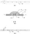
Fig. 6 is an enlarged view of part A inFig. 5 ; -
Fig. 7 is a top view ofEmbodiment 3 of a flexible LED flip flexible light bar of the present invention; -
Fig. 8 is a cross-sectional view of A-A inFig. 7 ; -
Fig. 9 is a top view ofEmbodiment 3 of a flexible LED flip flexible light bar of the present invention without a top insulating film; -
Fig. 10 is an enlarged view of part B inFig. 9 ; -
Fig. 11 is a stereogram ofEmbodiment 4 of a flexible LED flip flexible light bar of the present invention; and -
Fig. 12 is an enlarged view of part C inFig. 11 . - In the drawings:
1, flexible housing; 2, circuit board; 3, LED flip chip; 4, top insulating film; 5, conductive circuit layer; 6, bottom insulating film; 7, power line; 8, series line; 9, first through hole; 10, series line body; 11, solder branch; 11a, a portion of solder branches; 11b, another portion of solder branches; L, joint; 12, pad; 13, solder branch body; 14, toner glue; 15, chip resistor; 16, solder paste bump. - The technical solutions in the embodiments of the present invention will be clearly and completely described hereinbelow with the drawings in the embodiments of the present invention. It is apparent that the described embodiments are only part of the embodiments of the present invention, not all of the embodiments. On the basis of the embodiments of the present invention, all other embodiments obtained on the premise of no creative work of those of ordinary skill in the art fall within the scope of protection of the present invention.
- It should be noted that Embodiments 1-2 and 5, and
Figs. 1-3 will not form part of the present invention, but represent background art. -
Embodiment 1 is used in the case of high voltage (80-130V, 200-240V). Referring toFig. 1 and Fig. 2 , this embodiment provides a flexible LED light bar, including aflexible housing 1. Theflexible housing 1 is provided with acircuit board 2. At least oneLED flip chip 3 is arranged at an upper end of thecircuit board 2. TheLED flip chip 3 and thecircuit board 2 are connected together through a plurality of solder paste bumps 16. - Specifically, the
circuit board 2 is a PCB. If a PCB is used, a small piece of PCB may be fixed on a soft carrier tape to achieve bending of the light bar. - Specifically, wires on the
circuit board 2 are arranged at an equal interval, which is convenient for simplifying the production process of the assembly line and improving production efficiency. - Specifically, a minimum interval between two adjacent solder paste bumps 16 of the same
LED flip chip 3 is 0.12mm. This size may be changed according to different needs of the product and different sizes of the LED flip chip. - Specifically, an upper surface of the
LED flip chip 3 is also covered withtoner glue 14 for adjusting the color temperature and color of light, playing an insulating role, and protecting theLED flip chip 3. - The thickness of the
toner glue 14 is 2-5mm, and as the thickness is larger, the light emission is more uniform. Thetoner glue 14 is a soft glue. - Specifically, the
LED flip chip 3 is a blue-rayLED flip chip 3, and thetoner glue 14 is formed by mixing fluorescent powder in transparent silica gel. The color temperature and color of light may be adjusted by adding fluorescent powder to silica gel. Table 1 and Table 2 are two kinds of powder mixing record table.Table 1 White light type Fluorescent powder Anti-precip itation powder Diffusion powder Mixing silica gel Powder 1 Powder 2Powder 3Powder 1Powder 1 A component B component Mod el Dosage Model Dosage Model Dosage Model Dosage Model Dosage Model Dosage Model Dosage War m whit e SD Y54 8-15 0. 19g SSD R630 D1-1 0.008
3gDM -30 0.00 37g KM T-13 60A 0. 03 4g KM T-13 60B 0. 34g 76g 3.3 2g 1.48 g 13 . 6g 13 6g Table 2 White light type Fluorescent powder Anti-precipitation powder Diffusion powder Mixing silica gel Powder 1 Powder 2Powde r3 Powder 1 Powder 1 A component B component Model Dosage Model Dosage Model Dosage Model Dosage Model Dosage Model Dosage Model Dosage Warm white SD Y54 8-1 5 0. 19g SSD R630 D1-1 0.0 08 3g DM -30 0.00 37g KM T-13 60A 0. 03 4g KM T-13 60B 0.34g 76g 3.32g 1.48g 13.6g 136g Neutral white SD Y55 2-15 0. 19 g SSD R620 W 0.0 11 2g DM -30 0.00 96g KM T-13 60A 0. 07 2g KM T-13 60B 0. 72g 38 g 2.2 4g 1.92 g 14 . 4g 14 4g Pure white SD Y54 8-15 0. 19 g SSD R620 W 0.0 02 4g DM -30 0.01 17g KM T-13 60A 0. 07 6g KM T-13 60B 0. 76g 38 g 0.4 8g 2.34 g 15 . 2g 15 2g - Specifically, a minimum interval between the LED flip chips (3) is 0.08mm.
- According to the parameter specifications of the
LED flip chip 3 used, a suitable FPC orPCB 2 is selected and designed, the appropriate pad specifications of a soldering furnace are set, dispensing parameters are set, after all preparations are completed, soldering equipment, dispensing equipment and silicone shell molding equipment are started, theLED flip chip 3 and thecircuit board 2 are soldered together through solder paste, a substrate of theLED flip chip 3 is protected by dispensing, and finally, theflexible housing 1 is molded outside the entire product to complete the product production. When the product is powered on, theLED flip chip 3 converts electrical energy into light energy to achieve light emission. Theflexible housing 1 may be appropriately bent and deformed according to different materials of thecircuit board 2 selected inside, but it is necessary to avoid direct 90° right-angle bending. -
Embodiment 2 is used in the case of low voltage (12V, 24V, 36V), referring toFig. 3 , its structure is substantially the same as that ofEmbodiment 1, and the main difference is that: theflexible housing 1 is removed; and it has 350LED flip chips 3 adopting a series-parallel connection mode of 7-series and 50-parallel. - The structure of
Embodiment 3 is substantially the same as that ofEmbodiment 1, and the main difference is that: thecircuit board 2 is an FPC. - Referring to
Fig. 4 to Fig. 9 , specifically, the FPC includes a topinsulating film 4, an intermediateconductive circuit layer 5 and a bottom insulatingfilm 6. Theconductive circuit layer 5 includes twopower lines 7, and a plurality of series lines 8. TheLED flip chips 3 are soldered on the series lines 8. The topinsulating film 4 is provided with a first throughhole 9 corresponding to the position of eachLED flip chip 3. TheLED flip chips 3 are accommodated in the first throughholes 9. - Specifically, the
series line 8 includes aseries line body 10. An end of theseries line body 10 close to theLED flip chip 3 is extended with asolder branch 11. The width of thesolder branch 11 is less than that of theseries line body 10. TheLED flip chip 3 is soldered to an end of thesolder branch 11. Thethinner solder branch 11 of theseries line body 10 may serve as a force buffering portion. Since thesolder branch 11 is thinner and has higher flexibility, when anLED strip lamp 1 is bent, basically only theseries line body 10 is bent and forced. The force ofsoft solder branch 11 is extremely small, and thesolder branch 11 is used to solder the end of the flip-chipLED flip chip 3 with less stress, so that theLED flip chip 3 will not be cracked and broken by stress when theLED strip lamp 1 is bent like the chip LED, and the quality is more reliable. - Specifically, the top insulating
film 4 is pasted to cover a portion of thesolder branch 11 close to theseries line body 10. Because the width of thesolder branch 11 is different from that of theseries line body 10, when a joint between thesolder branch 11 and theseries line body 10 is bent multiple times, it is relatively more likely to be broken by an external force, just like easy breakage of a joint between a plug and a wire. The topinsulating film 4 is pasted to cover at least a portion ofsolder branch 11a close to theseries line body 10, and another portion ofsolder branch 11b is exposed in the first throughhole 9. A joint L between thesolder branch 11 and theseries line body 10 is pasted and protected by the top insulatingfilm 4, so that the joint L cannot be broken by an external force, and the quality is more reliable. - Specifically, an end of the
solder branch 11 close to theLED flip chip 3 is extended with apad 12, the width of thepad 12 is greater than that of asolder branch body 13 of thesolder branch 11, the length of thepad 12 is greater than or equal to the width of theLED flip chip 3, and an electrode of theLED flip chip 3 is directly soldered on thepad 12. On the premise of ensuring that theLED flip chip 3 has enough soldering area, thesolder branch 11 can be made softer to achieve a better force buffering effect, so that the soldering point of theLED flip chip 3 is less likely to be cracked by an external force during bending. - Specifically,
toner glue 14 is provided at a position corresponding to eachLED flip chip 3, and thetoner glue 14 covers at least theLED flip chip 3 and the first throughhole 9. - Specifically, a
chip resistor 15 is further included. Thechip resistor 15 is electrically connected laterally between theseries line 8 on the outermost side and thepower line 7. -
Embodiment 3 is a series solution in which theLED flip chips 3 are placed horizontally: thepower lines 7 and theseries lines 8 are located on the same level, thepower lines 7 are located on both sides of theseries lines 8, theLED flip chips 3 are connected in series through theseries lines 8 and then connected in parallel to the twopower lines 7, thesolder branches 11 extending from twoadjacent series lines 8 are not on the same straight line, the twosolder branches 11 are distributed in parallel up and down,pads 12 on the twosolder branches 11 are on the same straight line in an up-down direction, theLED flip chips 3 are horizontally soldered on the twopads 12, and the length direction of theLED flip chips 3 is consistent with the width direction of the FPC. - Referring to
Fig. 10 and Fig. 11 , its structure is substantially the same as that ofEmbodiment 3, and the main difference is that:Embodiment 4 is another series solution in which theLED flip chips 3 are placed vertically: thepower lines 7 are located on both sides of theseries lines 8, theLED flip chips 3 are connected in series through theseries lines 8 and then connected in parallel to the twopower lines 7, thesolder branches 11 extending from twoadjacent series lines 8 are on the same straight line, the width of thepad 12 is greater than that of theLED flip chips 3, theLED flip chips 3 are placed vertically, and the length direction of theLED flip chips 3 is consistent with the length direction of theFPC 2. - The structure of
Embodiment 5 is substantially the same as that ofEmbodiment 3, and the main difference is that:Embodiment 5 is a parallel solution: theLED flip chips 3 are connected in parallel to twopower lines 7 through parallel lines, respectively. - The structure of
Embodiment 6 is substantially the same as that ofEmbodiment 3, and the main difference is that:Embodiment 6 is another series solution in which theseries lines 8 and thepower lines 7 are separated into two layers: thepower lines 7 and theseries lines 8 are located on two different levels, the twopower lines 7 are located below theseries lines 8, theLED flip chips 3 are connected in series through theseries lines 8 and then connected to the twopower lines 7 in parallel, and an intermediate insulating film is disposed between thepower line 7 and theseries line 8. - Compared with the conventional art, the beneficial effects of the present invention are as follows.
- 1. The product structure and process are simple, the production yield rate is higher and the manufacturing cost is lower. The product structure is simplified, a conventional support structure is removed, an LED flip chip is used to be soldered directly to a circuit board through solder paste instead, the support fixing, solid crystal, welding wire and other processes are eliminated, the occurrence of defective products such as glue explosion, virtual welding, and vulcanization are reduced, the investment of production equipment and labor is reduced, and the purpose of reducing the production cost is achieved.
- 2. The assembly line production is realized. The production process is relatively simple, continuous production can be concentrated in the same production line, and the production efficiency is higher.
- 3. The application is wider. The structure product is suitable for FPCs and PCBs. The size of the circuit board and chip can be designed according to needs, and the application is wider.
- Although the embodiments of the present invention have been shown and described, those of ordinary skill in the art can understand that various changes, modifications, substitutions and variations can be made to these embodiments without departing from the present invention, and the scope of the present invention is defined by the appended claims and their equivalents.
Claims (8)
- An LED flexible light bar, comprising: a circuit board (2), wherein LED flip chips (3) are arranged at an upper end of the circuit board (2), and the LED flip chips (3) and the circuit board (2) are connected together by a plurality of solder paste bumps (16);the circuit board (2) is a Flexible Printed Circuit (FPC);the FPC comprises a top insulating film (4) and an intermediate conductive circuit layer (5) and a bottom insulating film (6), the conductive circuit layer (5) comprises two power lines (7), a plurality of series lines (8); the LED flip chips (3) are soldered on the series lines (8), the top insulating film (4) is provided with a first through hole (9) corresponding to the position of each LED flip chip (3), and the LED flip chips (3) are accommodated in the first through holes (9);each of the plurality of series lines (8) comprises a series line body (10), an end of the series line body (10) close to the LED flip chip (3) is extended with a solder branch (11); the width of the solder branch (11) is less than half of the width of the series line body (10) and the LED flip chip (3) is soldered to an end of the solder branch (11);the top insulating film (4) is pasted to cover a portion of the solder branch (11) close to the series line body (10);a joint (L) between the solder branch (11) and the series line body (10) is pasted and protected by the top insulating film (4).
- The LED flexible light bar according to claim 1, wherein the LED flip chips (3) are further covered with toner glues (14).
- The LED flexible light bar according to claim 2, the circuit board (2) is wrapped by a flexible housing (1).
- The LED flexible light bar according to claim 1, wherein wires on the circuit board (2) are arranged at an equal interval.
- The LED flexible light bar according to claim 1, wherein a minimum distance between two adjacent solder paste bumps (16) of the same LED flip chip (3) is 0.12mm.
- The LED flexible light bar according to claim 1, wherein a minimum interval between the LED flip chips (3) is 0.08mm.
- The LED flexible light bar according to claim 1, wherein an end of the solder branch (11) close to the LED flip chip (3) is extended with a pad (12), a width of the pad (12) is greater than that of a solder branch body (13) of the solder branch (11), the width or length of the pad (12) is greater than or equal to a width of the LED flip chip (3), and an electrode of the LED flip chip (3) is directly soldered on the pad (12).
- The LED flexible light bar according to claim 1, wherein toner glue (14) is provided at a position corresponding to each LED flip chip (3), the toner glue (14) covering at least the LED flip chip (3) and the first through hole (9);the power lines (7) and the series lines (8) are located on the same level, the power lines (7) are located on both sides of the series lines (8), the LED flip chips (3) are connected in series through the series lines (8) and then connected in parallel to the two power lines (7), the solder branches (11) extending from two adjacent series lines (8) are not on the same straight line, the two solder branches (11) are distributed in parallel up and down, the LED flip chips (3) are placed horizontally, and the length direction of the LED flip chips (3) is consistent with the width direction of the FPC; or, the solder branches (11) extending from two adjacent series lines (8) are on the same straight line, the LED flip chips (3) are placed vertically, and the length direction of the LED flip chips (3) is consistent with the length direction of the FPC;or, the power lines (7) and the series lines (8) are located on two different levels, the two power lines (7) are located below the series lines (8), and an intermediate insulating film is disposed between the power line (7) and the series lines (8).
Applications Claiming Priority (2)
| Application Number | Priority Date | Filing Date | Title |
|---|---|---|---|
| CN201920188844.1U CN209431157U (en) | 2019-02-10 | 2019-02-10 | A kind of flexible LED upside-down mounting soft light bar |
| PCT/CN2019/107120 WO2020160696A1 (en) | 2019-02-10 | 2019-09-20 | Flexible led light bar |
Publications (4)
| Publication Number | Publication Date |
|---|---|
| EP3719387A1 EP3719387A1 (en) | 2020-10-07 |
| EP3719387A4 EP3719387A4 (en) | 2021-06-02 |
| EP3719387B1 true EP3719387B1 (en) | 2024-07-10 |
| EP3719387C0 EP3719387C0 (en) | 2024-07-10 |
Family
ID=67977779
Family Applications (1)
| Application Number | Title | Priority Date | Filing Date |
|---|---|---|---|
| EP19880936.0A Active EP3719387B1 (en) | 2019-02-10 | 2019-09-20 | Flexible led light bar |
Country Status (6)
| Country | Link |
|---|---|
| US (1) | US11092318B2 (en) |
| EP (1) | EP3719387B1 (en) |
| JP (1) | JP7108326B2 (en) |
| CN (2) | CN209431157U (en) |
| AU (1) | AU2019382303B2 (en) |
| WO (1) | WO2020160696A1 (en) |
Families Citing this family (7)
| Publication number | Priority date | Publication date | Assignee | Title |
|---|---|---|---|---|
| CN209431157U (en) * | 2019-02-10 | 2019-09-24 | 中山市蓝德电子有限公司 | A kind of flexible LED upside-down mounting soft light bar |
| CN213040365U (en) * | 2020-05-26 | 2021-04-23 | 中山市卉彩光电科技有限公司 | Strip lamp of plastic |
| CN213394756U (en) * | 2020-11-10 | 2021-06-08 | 广东欧曼科技股份有限公司 | Fluorescent LED strips based on CSP or FC chips |
| CN112856264B (en) * | 2021-02-04 | 2025-03-04 | 广东大唐永恒智能科技有限公司 | A unitized flexible light strip and a manufacturing method thereof |
| CN113324190A (en) * | 2021-06-03 | 2021-08-31 | 中山市美耐特光电有限公司 | Flexible LED lamp area |
| CN114811472B (en) * | 2022-06-30 | 2022-09-20 | 深圳市兴连鑫光源有限公司 | Breakthrough soft lamp strip capable of realizing high-efficiency portable power supply |
| CN218671709U (en) * | 2022-11-17 | 2023-03-21 | 杨建保 | Line light-emitting lamp string |
Family Cites Families (38)
| Publication number | Priority date | Publication date | Assignee | Title |
|---|---|---|---|---|
| US3894225A (en) * | 1974-07-11 | 1975-07-08 | Albert L Chao | Tape-lamps |
| EP1590994B1 (en) * | 2003-02-07 | 2016-05-18 | Panasonic Intellectual Property Management Co., Ltd. | Metal base wiring board for retaining light emitting elements, light emitting source, lighting apparatus, and display apparatus |
| TWI224661B (en) * | 2003-06-13 | 2004-12-01 | Yuan Lin | Multi-channel light source based longitudinal lighting device |
| KR101230617B1 (en) * | 2006-06-30 | 2013-02-06 | 서울반도체 주식회사 | Light emitting diode and Method of manufacturing the same |
| US8052303B2 (en) | 2006-09-12 | 2011-11-08 | Huizhou Light Engine Ltd. | Integrally formed single piece light emitting diode light wire and uses thereof |
| TW200939869A (en) * | 2008-03-05 | 2009-09-16 | Harvatek Corp | An LED chip package structure with a high-efficiency heat-dissipating substrate and packaging method thereof |
| US20120009700A1 (en) * | 2009-04-17 | 2012-01-12 | Harvatek Corporation | Method of manufacturing a led chip package structure |
| WO2011111399A1 (en) * | 2010-03-11 | 2011-09-15 | パナソニック株式会社 | Light emitting module, light source device, liquid crystal display device, and method for manufacturing light emitting module |
| KR20110129273A (en) | 2010-05-25 | 2011-12-01 | 삼성엘이디 주식회사 | LED light source module and lighting device having same |
| CN102064164B (en) * | 2010-10-28 | 2012-03-21 | 山东华光光电子有限公司 | Freely combined lamp wick of flip-chip power LED tube core |
| US20140209928A1 (en) * | 2011-09-22 | 2014-07-31 | The Silanna Group Pty Ltd | Light source assembly and a process for producing a light source assembly |
| JP6209874B2 (en) * | 2012-08-31 | 2017-10-11 | 日亜化学工業株式会社 | Light emitting device and manufacturing method thereof |
| US8947001B2 (en) * | 2012-09-06 | 2015-02-03 | Cooledge Lighting Inc. | Wiring boards for array-based electronic devices |
| JP6060578B2 (en) * | 2012-09-14 | 2017-01-18 | 日亜化学工業株式会社 | Light emitting device |
| JP6079159B2 (en) | 2012-11-16 | 2017-02-15 | 日亜化学工業株式会社 | Light emitting device |
| TW201431042A (en) | 2013-01-25 | 2014-08-01 | 廖旭文 | Double-sided light-emitting LED light board structure and manufacturing method thereof |
| JP5503760B1 (en) * | 2013-02-06 | 2014-05-28 | 三菱化工機株式会社 | LIGHT SOURCE DEVICE, LIGHTING DEVICE EQUIPPED WITH THE SAME, AND METHOD FOR MANUFACTURING LIGHT SOURCE DEVICE |
| US8998454B2 (en) * | 2013-03-15 | 2015-04-07 | Sumitomo Electric Printed Circuits, Inc. | Flexible electronic assembly and method of manufacturing the same |
| US8928014B2 (en) | 2013-03-15 | 2015-01-06 | Cooledge Lighting Inc. | Stress relief for array-based electronic devices |
| TWI626395B (en) * | 2013-06-11 | 2018-06-11 | 晶元光電股份有限公司 | Illuminating device |
| CN203377266U (en) * | 2013-06-18 | 2014-01-01 | 上海鼎晖科技股份有限公司 | Flexible COB (chip on board) packaging LED |
| CN203384752U (en) * | 2013-07-15 | 2014-01-08 | 厦门乾照光电股份有限公司 | LED soft lamp strip |
| CN203631589U (en) * | 2013-09-30 | 2014-06-04 | 泉州市金太阳照明科技有限公司 | Inverted LED packaging structure and LED lamp strip |
| US10134714B2 (en) * | 2013-11-08 | 2018-11-20 | Osram Sylvania Inc. | Flexible circuit board for LED lighting fixtures |
| CN203641957U (en) * | 2013-12-02 | 2014-06-11 | 曾卓焱 | Flexible LED (light emitting diode) lamp strip |
| JP6431485B2 (en) * | 2013-12-02 | 2018-11-28 | 東芝ホクト電子株式会社 | Light emitting device |
| JP6343923B2 (en) | 2013-12-18 | 2018-06-20 | 日亜化学工業株式会社 | Light emitting device |
| JP6414485B2 (en) | 2015-02-27 | 2018-10-31 | 日亜化学工業株式会社 | Light emitting device |
| US10036546B2 (en) * | 2015-11-18 | 2018-07-31 | Koito Manufacturing Co., Ltd. | Lamp and manufacturing method thereof |
| CN206918680U (en) | 2015-12-19 | 2018-01-23 | 嘉兴山蒲照明电器有限公司 | LEDbulb lamp |
| CN105720174A (en) * | 2016-04-20 | 2016-06-29 | 漳州立达信光电子科技有限公司 | LED surface light source and preparation method thereof |
| CN205877838U (en) | 2016-04-29 | 2017-01-11 | 郭垣成 | FPCCOB lamp area |
| JP7014948B2 (en) | 2017-06-13 | 2022-02-02 | 日亜化学工業株式会社 | Manufacturing method of light emitting device and light emitting device |
| CN207962198U (en) * | 2018-03-06 | 2018-10-12 | 东莞市伊伯光电科技有限公司 | A new type of flexible light bar |
| CN109140279A (en) * | 2018-08-24 | 2019-01-04 | 重庆秉为科技有限公司 | A kind of LED light with flexible filament |
| CN109268718A (en) * | 2018-09-30 | 2019-01-25 | 惠州市鹏程电子科技有限公司 | LED soft light rope and preparation method thereof |
| CN109519742A (en) * | 2018-12-09 | 2019-03-26 | 江门朗天照明有限公司 | A kind of strip light with flip LED chips |
| CN209431157U (en) * | 2019-02-10 | 2019-09-24 | 中山市蓝德电子有限公司 | A kind of flexible LED upside-down mounting soft light bar |
-
2019
- 2019-02-10 CN CN201920188844.1U patent/CN209431157U/en active Active
- 2019-09-20 CN CN201980005293.3A patent/CN111670319A/en active Pending
- 2019-09-20 WO PCT/CN2019/107120 patent/WO2020160696A1/en not_active Ceased
- 2019-09-20 JP JP2020530967A patent/JP7108326B2/en not_active Expired - Fee Related
- 2019-09-20 EP EP19880936.0A patent/EP3719387B1/en active Active
- 2019-09-20 AU AU2019382303A patent/AU2019382303B2/en not_active Ceased
-
2020
- 2020-05-24 US US16/882,532 patent/US11092318B2/en active Active
Also Published As
| Publication number | Publication date |
|---|---|
| JP2021516415A (en) | 2021-07-01 |
| CN111670319A (en) | 2020-09-15 |
| AU2019382303B2 (en) | 2021-11-04 |
| AU2019382303A1 (en) | 2020-08-27 |
| WO2020160696A1 (en) | 2020-08-13 |
| US20200284407A1 (en) | 2020-09-10 |
| US11092318B2 (en) | 2021-08-17 |
| JP7108326B2 (en) | 2022-07-28 |
| EP3719387C0 (en) | 2024-07-10 |
| EP3719387A4 (en) | 2021-06-02 |
| CN209431157U (en) | 2019-09-24 |
| EP3719387A1 (en) | 2020-10-07 |
Similar Documents
| Publication | Publication Date | Title |
|---|---|---|
| AU2019382303B2 (en) | LED flexible light bar | |
| US11444008B2 (en) | Semiconductor light emitting device and method for manufacturing the same | |
| CN107275322A (en) | Side-emitting programmable control LED with IC | |
| JP2005109282A5 (en) | ||
| JP2011096901A (en) | Flexible led module and unit led module | |
| CN112366201B (en) | High-power light source packaging structure and manufacturing method thereof | |
| CN201226357Y (en) | Light emitting diode chip packaging structure for backlight module | |
| CN206976341U (en) | The luminous PLC technology LED in side with IC | |
| CN218351465U (en) | LED lamp bead and LED lamp strip | |
| CN218849491U (en) | LED lamp beads and LED strips | |
| CN206130651U (en) | LED light -emitting component , LED lighting strip and LED luminescent panel | |
| US11415276B2 (en) | Flexible light strip made of fluorescent material | |
| CN201780992U (en) | Package structure of series flexible light-emitting diodes | |
| CN217691174U (en) | LED lamp bead and LED lamp strip | |
| WO2008074218A1 (en) | Light emitting stick having led chips | |
| CN217655877U (en) | LED lamp bead and LED lamp strip | |
| CN119421579B (en) | LED lamp bead, preparation method thereof and display screen | |
| CN211232492U (en) | COB lamp strip | |
| CN213546351U (en) | LED and support, lead assembly, LED module and light-emitting device thereof | |
| CN202196812U (en) | Strip-shaped light-emitting structure | |
| CN210926010U (en) | Four-color single-drive stage lamp | |
| CN210040192U (en) | Novel high-brightness small-interval SMD-LED light-emitting unit | |
| CN112838081A (en) | A kind of encapsulated digital chip LED and its packaging method | |
| CN107146837B (en) | A double-sided side-emission LED light source unit and its manufacturing method | |
| CN206584952U (en) | A LED light source unit with double-sided side-emission |
Legal Events
| Date | Code | Title | Description |
|---|---|---|---|
| STAA | Information on the status of an ep patent application or granted ep patent |
Free format text: STATUS: UNKNOWN |
|
| STAA | Information on the status of an ep patent application or granted ep patent |
Free format text: STATUS: THE INTERNATIONAL PUBLICATION HAS BEEN MADE |
|
| PUAI | Public reference made under article 153(3) epc to a published international application that has entered the european phase |
Free format text: ORIGINAL CODE: 0009012 |
|
| STAA | Information on the status of an ep patent application or granted ep patent |
Free format text: STATUS: REQUEST FOR EXAMINATION WAS MADE |
|
| 17P | Request for examination filed |
Effective date: 20200519 |
|
| AK | Designated contracting states |
Kind code of ref document: A1 Designated state(s): AL AT BE BG CH CY CZ DE DK EE ES FI FR GB GR HR HU IE IS IT LI LT LU LV MC MK MT NL NO PL PT RO RS SE SI SK SM TR |
|
| AX | Request for extension of the european patent |
Extension state: BA ME |
|
| A4 | Supplementary search report drawn up and despatched |
Effective date: 20210430 |
|
| RIC1 | Information provided on ipc code assigned before grant |
Ipc: F21S 4/24 20160101AFI20210423BHEP Ipc: F21K 9/90 20160101ALI20210423BHEP Ipc: F21V 23/00 20150101ALI20210423BHEP Ipc: F21V 23/06 20060101ALI20210423BHEP Ipc: F21Y 103/10 20160101ALN20210423BHEP Ipc: F21Y 115/10 20160101ALN20210423BHEP |
|
| DAV | Request for validation of the european patent (deleted) | ||
| DAX | Request for extension of the european patent (deleted) | ||
| STAA | Information on the status of an ep patent application or granted ep patent |
Free format text: STATUS: EXAMINATION IS IN PROGRESS |
|
| 17Q | First examination report despatched |
Effective date: 20220627 |
|
| GRAP | Despatch of communication of intention to grant a patent |
Free format text: ORIGINAL CODE: EPIDOSNIGR1 |
|
| STAA | Information on the status of an ep patent application or granted ep patent |
Free format text: STATUS: GRANT OF PATENT IS INTENDED |
|
| RIC1 | Information provided on ipc code assigned before grant |
Ipc: F21Y 115/10 20160101ALN20240131BHEP Ipc: F21Y 103/10 20160101ALN20240131BHEP Ipc: F21V 23/06 20060101ALI20240131BHEP Ipc: F21V 23/00 20150101ALI20240131BHEP Ipc: F21K 9/90 20160101ALI20240131BHEP Ipc: F21S 4/24 20160101AFI20240131BHEP |
|
| INTG | Intention to grant announced |
Effective date: 20240219 |
|
| GRAS | Grant fee paid |
Free format text: ORIGINAL CODE: EPIDOSNIGR3 |
|
| GRAA | (expected) grant |
Free format text: ORIGINAL CODE: 0009210 |
|
| STAA | Information on the status of an ep patent application or granted ep patent |
Free format text: STATUS: THE PATENT HAS BEEN GRANTED |
|
| AK | Designated contracting states |
Kind code of ref document: B1 Designated state(s): AL AT BE BG CH CY CZ DE DK EE ES FI FR GB GR HR HU IE IS IT LI LT LU LV MC MK MT NL NO PL PT RO RS SE SI SK SM TR |
|
| REG | Reference to a national code |
Ref country code: CH Ref legal event code: EP |
|
| REG | Reference to a national code |
Ref country code: DE Ref legal event code: R096 Ref document number: 602019055146 Country of ref document: DE |
|
| U01 | Request for unitary effect filed |
Effective date: 20240807 |
|
| U07 | Unitary effect registered |
Designated state(s): AT BE BG DE DK EE FI FR IT LT LU LV MT NL PT SE SI Effective date: 20240820 |
|
| U21 | Renewal fee for the european patent with unitary effect paid with additional fee |
Year of fee payment: 6 Effective date: 20241125 |
|
| PG25 | Lapsed in a contracting state [announced via postgrant information from national office to epo] |
Ref country code: NO Free format text: LAPSE BECAUSE OF FAILURE TO SUBMIT A TRANSLATION OF THE DESCRIPTION OR TO PAY THE FEE WITHIN THE PRESCRIBED TIME-LIMIT Effective date: 20241010 |
|
| PG25 | Lapsed in a contracting state [announced via postgrant information from national office to epo] |
Ref country code: PL Free format text: LAPSE BECAUSE OF FAILURE TO SUBMIT A TRANSLATION OF THE DESCRIPTION OR TO PAY THE FEE WITHIN THE PRESCRIBED TIME-LIMIT Effective date: 20240710 Ref country code: GR Free format text: LAPSE BECAUSE OF FAILURE TO SUBMIT A TRANSLATION OF THE DESCRIPTION OR TO PAY THE FEE WITHIN THE PRESCRIBED TIME-LIMIT Effective date: 20241011 |
|
| PG25 | Lapsed in a contracting state [announced via postgrant information from national office to epo] |
Ref country code: IS Free format text: LAPSE BECAUSE OF FAILURE TO SUBMIT A TRANSLATION OF THE DESCRIPTION OR TO PAY THE FEE WITHIN THE PRESCRIBED TIME-LIMIT Effective date: 20241110 |
|
| PG25 | Lapsed in a contracting state [announced via postgrant information from national office to epo] |
Ref country code: HR Free format text: LAPSE BECAUSE OF FAILURE TO SUBMIT A TRANSLATION OF THE DESCRIPTION OR TO PAY THE FEE WITHIN THE PRESCRIBED TIME-LIMIT Effective date: 20240710 |
|
| PG25 | Lapsed in a contracting state [announced via postgrant information from national office to epo] |
Ref country code: RS Free format text: LAPSE BECAUSE OF FAILURE TO SUBMIT A TRANSLATION OF THE DESCRIPTION OR TO PAY THE FEE WITHIN THE PRESCRIBED TIME-LIMIT Effective date: 20241010 Ref country code: ES Free format text: LAPSE BECAUSE OF FAILURE TO SUBMIT A TRANSLATION OF THE DESCRIPTION OR TO PAY THE FEE WITHIN THE PRESCRIBED TIME-LIMIT Effective date: 20240710 |
|
| PG25 | Lapsed in a contracting state [announced via postgrant information from national office to epo] |
Ref country code: RS Free format text: LAPSE BECAUSE OF FAILURE TO SUBMIT A TRANSLATION OF THE DESCRIPTION OR TO PAY THE FEE WITHIN THE PRESCRIBED TIME-LIMIT Effective date: 20241010 Ref country code: PL Free format text: LAPSE BECAUSE OF FAILURE TO SUBMIT A TRANSLATION OF THE DESCRIPTION OR TO PAY THE FEE WITHIN THE PRESCRIBED TIME-LIMIT Effective date: 20240710 Ref country code: NO Free format text: LAPSE BECAUSE OF FAILURE TO SUBMIT A TRANSLATION OF THE DESCRIPTION OR TO PAY THE FEE WITHIN THE PRESCRIBED TIME-LIMIT Effective date: 20241010 Ref country code: IS Free format text: LAPSE BECAUSE OF FAILURE TO SUBMIT A TRANSLATION OF THE DESCRIPTION OR TO PAY THE FEE WITHIN THE PRESCRIBED TIME-LIMIT Effective date: 20241110 Ref country code: HR Free format text: LAPSE BECAUSE OF FAILURE TO SUBMIT A TRANSLATION OF THE DESCRIPTION OR TO PAY THE FEE WITHIN THE PRESCRIBED TIME-LIMIT Effective date: 20240710 Ref country code: GR Free format text: LAPSE BECAUSE OF FAILURE TO SUBMIT A TRANSLATION OF THE DESCRIPTION OR TO PAY THE FEE WITHIN THE PRESCRIBED TIME-LIMIT Effective date: 20241011 Ref country code: ES Free format text: LAPSE BECAUSE OF FAILURE TO SUBMIT A TRANSLATION OF THE DESCRIPTION OR TO PAY THE FEE WITHIN THE PRESCRIBED TIME-LIMIT Effective date: 20240710 |
|
| PG25 | Lapsed in a contracting state [announced via postgrant information from national office to epo] |
Ref country code: SM Free format text: LAPSE BECAUSE OF FAILURE TO SUBMIT A TRANSLATION OF THE DESCRIPTION OR TO PAY THE FEE WITHIN THE PRESCRIBED TIME-LIMIT Effective date: 20240710 |
|
| PG25 | Lapsed in a contracting state [announced via postgrant information from national office to epo] |
Ref country code: MC Free format text: LAPSE BECAUSE OF FAILURE TO SUBMIT A TRANSLATION OF THE DESCRIPTION OR TO PAY THE FEE WITHIN THE PRESCRIBED TIME-LIMIT Effective date: 20240710 |
|
| PG25 | Lapsed in a contracting state [announced via postgrant information from national office to epo] |
Ref country code: CZ Free format text: LAPSE BECAUSE OF FAILURE TO SUBMIT A TRANSLATION OF THE DESCRIPTION OR TO PAY THE FEE WITHIN THE PRESCRIBED TIME-LIMIT Effective date: 20240710 |
|
| PG25 | Lapsed in a contracting state [announced via postgrant information from national office to epo] |
Ref country code: SK Free format text: LAPSE BECAUSE OF FAILURE TO SUBMIT A TRANSLATION OF THE DESCRIPTION OR TO PAY THE FEE WITHIN THE PRESCRIBED TIME-LIMIT Effective date: 20240710 |
|
| REG | Reference to a national code |
Ref country code: CH Ref legal event code: PL |
|
| PLBE | No opposition filed within time limit |
Free format text: ORIGINAL CODE: 0009261 |
|
| STAA | Information on the status of an ep patent application or granted ep patent |
Free format text: STATUS: NO OPPOSITION FILED WITHIN TIME LIMIT |
|
| 26N | No opposition filed |
Effective date: 20250411 |
|
| GBPC | Gb: european patent ceased through non-payment of renewal fee |
Effective date: 20241010 |
|
| U1N | Appointed representative for the unitary patent procedure changed after the registration of the unitary effect |
Representative=s name: METIDA; LT |
|
| PG25 | Lapsed in a contracting state [announced via postgrant information from national office to epo] |
Ref country code: GB Free format text: LAPSE BECAUSE OF NON-PAYMENT OF DUE FEES Effective date: 20241010 |
|
| PG25 | Lapsed in a contracting state [announced via postgrant information from national office to epo] |
Ref country code: CH Free format text: LAPSE BECAUSE OF NON-PAYMENT OF DUE FEES Effective date: 20240930 |
|
| PG25 | Lapsed in a contracting state [announced via postgrant information from national office to epo] |
Ref country code: IE Free format text: LAPSE BECAUSE OF NON-PAYMENT OF DUE FEES Effective date: 20240920 |
|
| PG25 | Lapsed in a contracting state [announced via postgrant information from national office to epo] |
Ref country code: RO Free format text: LAPSE BECAUSE OF FAILURE TO SUBMIT A TRANSLATION OF THE DESCRIPTION OR TO PAY THE FEE WITHIN THE PRESCRIBED TIME-LIMIT Effective date: 20240710 |
|
| PG25 | Lapsed in a contracting state [announced via postgrant information from national office to epo] |
Ref country code: CY Free format text: LAPSE BECAUSE OF FAILURE TO SUBMIT A TRANSLATION OF THE DESCRIPTION OR TO PAY THE FEE WITHIN THE PRESCRIBED TIME-LIMIT; INVALID AB INITIO Effective date: 20190920 |
|
| PG25 | Lapsed in a contracting state [announced via postgrant information from national office to epo] |
Ref country code: HU Free format text: LAPSE BECAUSE OF FAILURE TO SUBMIT A TRANSLATION OF THE DESCRIPTION OR TO PAY THE FEE WITHIN THE PRESCRIBED TIME-LIMIT; INVALID AB INITIO Effective date: 20190920 |