EP3716319A1 - Bipolartransistormodul mit isoliertem gate, dafür vorgesehene leiterinstallationsstruktur und wechselrichter - Google Patents
Bipolartransistormodul mit isoliertem gate, dafür vorgesehene leiterinstallationsstruktur und wechselrichter Download PDFInfo
- Publication number
- EP3716319A1 EP3716319A1 EP20155032.4A EP20155032A EP3716319A1 EP 3716319 A1 EP3716319 A1 EP 3716319A1 EP 20155032 A EP20155032 A EP 20155032A EP 3716319 A1 EP3716319 A1 EP 3716319A1
- Authority
- EP
- European Patent Office
- Prior art keywords
- conductor
- insulation
- substrate
- igbt module
- installing structure
- Prior art date
- Legal status (The legal status is an assumption and is not a legal conclusion. Google has not performed a legal analysis and makes no representation as to the accuracy of the status listed.)
- Pending
Links
Images




Classifications
-
- H—ELECTRICITY
- H10—SEMICONDUCTOR DEVICES; ELECTRIC SOLID-STATE DEVICES NOT OTHERWISE PROVIDED FOR
- H10W—GENERIC PACKAGES, INTERCONNECTIONS, CONNECTORS OR OTHER CONSTRUCTIONAL DETAILS OF DEVICES COVERED BY CLASS H10
- H10W76/00—Containers; Fillings or auxiliary members therefor; Seals
- H10W76/10—Containers or parts thereof
- H10W76/12—Containers or parts thereof characterised by their shape
-
- H—ELECTRICITY
- H02—GENERATION; CONVERSION OR DISTRIBUTION OF ELECTRIC POWER
- H02M—APPARATUS FOR CONVERSION BETWEEN AC AND AC, BETWEEN AC AND DC, OR BETWEEN DC AND DC, AND FOR USE WITH MAINS OR SIMILAR POWER SUPPLY SYSTEMS; CONVERSION OF DC OR AC INPUT POWER INTO SURGE OUTPUT POWER; CONTROL OR REGULATION THEREOF
- H02M7/00—Conversion of AC power input into DC power output; Conversion of DC power input into AC power output
- H02M7/42—Conversion of DC power input into AC power output without possibility of reversal
- H02M7/44—Conversion of DC power input into AC power output without possibility of reversal by static converters
- H02M7/48—Conversion of DC power input into AC power output without possibility of reversal by static converters using discharge tubes with control electrode or semiconductor devices with control electrode
- H02M7/53—Conversion of DC power input into AC power output without possibility of reversal by static converters using discharge tubes with control electrode or semiconductor devices with control electrode using devices of a triode or transistor type requiring continuous application of a control signal
- H02M7/537—Conversion of DC power input into AC power output without possibility of reversal by static converters using discharge tubes with control electrode or semiconductor devices with control electrode using devices of a triode or transistor type requiring continuous application of a control signal using semiconductor devices only, e.g. single switched pulse inverters
-
- H—ELECTRICITY
- H05—ELECTRIC TECHNIQUES NOT OTHERWISE PROVIDED FOR
- H05K—PRINTED CIRCUITS; CASINGS OR CONSTRUCTIONAL DETAILS OF ELECTRIC APPARATUS; MANUFACTURE OF ASSEMBLAGES OF ELECTRICAL COMPONENTS
- H05K1/00—Printed circuits
- H05K1/02—Details
- H05K1/11—Printed elements for providing electric connections to or between printed circuits
- H05K1/111—Pads for surface mounting, e.g. lay-out
-
- H—ELECTRICITY
- H10—SEMICONDUCTOR DEVICES; ELECTRIC SOLID-STATE DEVICES NOT OTHERWISE PROVIDED FOR
- H10D—INORGANIC ELECTRIC SEMICONDUCTOR DEVICES
- H10D84/00—Integrated devices formed in or on semiconductor substrates that comprise only semiconducting layers, e.g. on Si wafers or on GaAs-on-Si wafers
- H10D84/60—Integrated devices formed in or on semiconductor substrates that comprise only semiconducting layers, e.g. on Si wafers or on GaAs-on-Si wafers characterised by the integration of at least one component covered by groups H10D10/00 or H10D18/00, e.g. integration of BJTs
-
- H—ELECTRICITY
- H05—ELECTRIC TECHNIQUES NOT OTHERWISE PROVIDED FOR
- H05K—PRINTED CIRCUITS; CASINGS OR CONSTRUCTIONAL DETAILS OF ELECTRIC APPARATUS; MANUFACTURE OF ASSEMBLAGES OF ELECTRICAL COMPONENTS
- H05K2201/00—Indexing scheme relating to printed circuits covered by H05K1/00
- H05K2201/09—Shape and layout
- H05K2201/09209—Shape and layout details of conductors
- H05K2201/09654—Shape and layout details of conductors covering at least two types of conductors provided for in H05K2201/09218 - H05K2201/095
- H05K2201/09663—Divided layout, i.e. conductors divided in two or more parts
-
- H—ELECTRICITY
- H10—SEMICONDUCTOR DEVICES; ELECTRIC SOLID-STATE DEVICES NOT OTHERWISE PROVIDED FOR
- H10W—GENERIC PACKAGES, INTERCONNECTIONS, CONNECTORS OR OTHER CONSTRUCTIONAL DETAILS OF DEVICES COVERED BY CLASS H10
- H10W72/00—Interconnections or connectors in packages
- H10W72/90—Bond pads, in general
- H10W72/931—Shapes of bond pads
- H10W72/932—Plan-view shape, i.e. in top view
-
- Y—GENERAL TAGGING OF NEW TECHNOLOGICAL DEVELOPMENTS; GENERAL TAGGING OF CROSS-SECTIONAL TECHNOLOGIES SPANNING OVER SEVERAL SECTIONS OF THE IPC; TECHNICAL SUBJECTS COVERED BY FORMER USPC CROSS-REFERENCE ART COLLECTIONS [XRACs] AND DIGESTS
- Y02—TECHNOLOGIES OR APPLICATIONS FOR MITIGATION OR ADAPTATION AGAINST CLIMATE CHANGE
- Y02E—REDUCTION OF GREENHOUSE GAS [GHG] EMISSIONS, RELATED TO ENERGY GENERATION, TRANSMISSION OR DISTRIBUTION
- Y02E10/00—Energy generation through renewable energy sources
- Y02E10/50—Photovoltaic [PV] energy
- Y02E10/56—Power conversion systems, e.g. maximum power point trackers
Definitions
- the present disclosure relates to the field of photovoltaic grid-connection technology, particularly to an insulated gate bipolar transistor (IGBT) module, a conductor installing structure for the IGBT module, and an inverter.
- IGBT insulated gate bipolar transistor
- an inverter In a grid-connection photovoltaic generation system, an inverter is used as an interface device between the photovoltaic generation system and a power grid. In application, the inverter should meet requirements of safety regulations.
- the photovoltaic generation system has a high voltage
- an IGBT module of the inverter can hardly meet the requirements of safety regulations. Specifically, creepage distance of the IGBT module can hardly meet the requirement of safety regulations.
- insulation varnish or insulation paste is sprayed on the surface of the IGBT module to insulate and isolate a conductor from a substrate, so as to improve the comparative tracking index of the IGBT module, thereby improving the creepage distance of the IGBT module to meet the requirement.
- the uniformity of the spaying process is difficult to control, and thus the effectiveness of spraying is hard to determine.
- an adhesion of the insulation varnish or the insulation paste to the substrate is insufficient, which may easily result in a crack. Therefore, it is hard to determine whether the sprayed IGBT module meets the requirements of safety regulations, having a risk of insulation failure, which may cause a failure of the inverter and a low reliability.
- a conductor installing structure for an IGBT module is provided according to the present disclosure to increase the creepage distance of the IGBT module and improve insulation reliability.
- an IGBT module with the conductor installing structure and an inverter with the IGBT module are also provided.
- the conductor installing structure for an IGBT module includes a substrate, a conductor and an insulation sleeve sleeved on the conductor and insulatedly isolating the conductor from the substrate.
- the insulation sleeve is fixed on the substrate.
- the insulation sleeve includes: an insulation bushing sleeved on the conductor, and an insulation plate fixed with the circumferential side wall of the insulation bushing.
- the insulation plate is arranged on an installing surface of the substrate where the conductor is located.
- the insulation plate on one side closing to the edge of the substrate, has an outer extension, and the outer extension protrudes out of the outside edge of the installing surface of the substrate where the conductor is located.
- At least one of the insulation plate and the insulation bushing is fixed on the substrate.
- the insulation plate in a case that the insulation plate is fixed on the substrate, the insulation plate is fixed on the substrate by a snap engagement.
- the insulation plate is arranged with a step structure having a snap engagement with the substrate.
- the insulation bushing in a case that the insulation bushing is fixed on the substrate, the insulation bushing is inserted in a groove of the substrate.
- the top of the insulation plate is arranged with a supporting projection for supporting a circuit board of the IGBT module.
- a cross section of the insulation bushing (31) is square, rectangular or circular.
- the conductor installing structure for the IGBT module by using the insulation sleeve sleeved on the conductor to insulatedly isolate the conductor from the substrate, the comparative tracking index of the IGBT module is improved, thereby improving the creepage distance of the IGBT module.
- the insulating property of the insulation sleeve can be better detected and guaranteed, and the bonding between the insulation sleeve and the substrate can be better enhanced, improving the insulation reliability.
- an IGBT module including any of the above conductor installing structures is further provided.
- an inverter including the above IGBT module is provided.
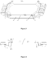
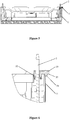
- a conductor installing structure for an IGBT module includes a substrate 1, a conductor 2 and an insulation sleeve 3 sleeved on the conductor 2 and insulatedly isolating the conductor 2 from the substrate 1.
- the conductor installing structure for the IGBT module by using the insulation sleeve 3 sleeved on the conductor 2 to insulatedly isolate the conductor 2 from the substrate 1, the comparative tracking index of the IGBT module is improved, thereby improving the creepage distance of the IGBT module.
- the insulating property of the insulation sleeve 3 can be better detected and guaranteed, and the bonding between the insulation sleeve 3 and the substrate 1 can be better enhanced, improving the insulation reliability.
- the insulation sleeve 3 includes: an insulation bushing 31 sleeved on the conductor 2, and an insulation plate 32 fixeded with the circumferential side wall of the insulation bushing 31.
- the insulation plate 32 is arranged on an installing surface of the substrate 1 where the conductor 2 is located.
- the insulation plate 32 and the insulation bushing 31 may have or not have a one-to-one correspondence.
- the insulation sleeve 3 may only include the insulation bushing 31 without the insulation plate 32, which is not limited to the above embodiments.
- the insulation plate 32 on one side closing to the edge of the substrate 1, has an outer extension 35, and the outer extension 35 protrudes out of the outside edge 11 of the installing surface of the substrate 1 where the conductor 2 is located.
- the outside edge 11 refers to the side of the installing surface that is close to the edge of the substrate 1, that is, the outside edge 11 refers to the side of the installing surface that is far away from the center of the substrate 1.
- the creepage safety regulation distance of the entire IGBT module is increased, thereby further improving the safety of the IGBT module.
- safety regulation requirements on distances for different voltage levels can be met by adjusting the size of the outer extension 35, which improves universality.
- the length by which the outer extension 35 protrudes out of the outside edge 11 is determined according to the distance required in safety regulations, which is not limited herein.
- the outer extension 35 and the insulation plate 32 may be implemented in a one-piece structure or may be implemented as two separate parts insulatedly connected with each other.
- the inside edge of the insulation plate 32 that is close to the center of the substrate 1 is level with the insulation bushing 31, as shown in Figure 6 .
- a side of the insulation bushing 31 that is away from the edge of the substrate 1, i.e., a side of the insulation bushing 31 that is close to the center of the substrate 1, may be arranged with an opening or not, which is determined according to actual requirements and is not limited herein.
- the opening and the outer extension 35 are respectively arranged in two sides of an axis of the insulation bushing 31.
- the size and shape of the opening may be determined according to actual requirements, which is not limited herein.
- the lower part of the inner bore of the insulation bushing 31 is formed to be gradually wider from the top of the substrate 1 to the bottom of the substrate 1, as shown in Figure 6 .
- the inner bore of the insulation bushing 31 may be in other shapes, which is not limited herein.
- the insulation sleeve 3 is fixed to the IGBT module to ensure reliability.
- the insulation sleeve 3 is preferably fixed on the substrate 1.
- the insulation plate 32 is preferably fixed on the substrate 1, that is, the whole insulation sleeve 3 is fixed on the substrate 1 by fixing the insulation plate 32 on the substrate 1.
- the manner of fixing the insulation plate 32 may be determined according to actual requirements.
- the insulation plate 32 may be fixed by a snap engagement, an adhering connection, and the like.
- the snap engagement is preferably used to fix the insulation plate 32 on the substrate 1.
- the insulation plate 32 may be arranged with a step structure 34 to have a snap engagement with the substrate 1, in order to achieve a simple and convenient installation.
- the snap engagement between the insulation plate 32 and the substrate 1 may be achieved by other snap engagement structures, such as a snapping hook, a snapping groove, and the like, which is not limited herein.
- the insulation sleeve 3 may be fixed on the substrate 1 by the insulation bushing 31. That is, the whole insulation sleeve 3 is fixed on the substrate 1 by fixing the insulation bushing 31 on the substrate 1.
- the insulation sleeve 3 is inserted in a groove of the substrate 1. Therefore, an existing groove in the substrate 1 is utilized, which simplifies the structure and facilitates the fixing.
- the insulation bushing 31 may be fixed to the substrate 1 in other manners, which is not limited herein.
- the bottom of the insulation bushing 31 extends out from the bottom of the insulation plate 32.
- the top of the insulation bushing 31 may be level with the insulation plate 32 or extend out from the top of the insulation plate 32.
- the insulation plate 32 and the insulation bushing 31 are preferably both fixed on the substrate 1.
- the top of the insulation plate 32 is arranged with a supporting projection 33 for supporting the circuit board of the IGBT module.
- the number and shape of the supporting projection 33 are determined according to actual requirements. For example, when the insulation plate 32 is square, there are preferably four supporting projections 33, and the four supporting projection are located in the vertex angles of the insulation plate 32, which is not limited herein.
- the circuit board is supported by the supporting projection 33, and also the circuit board compresses the insulation plate 32, which improves the fixing reliability.
- the shapes of the insulation bushing 31 and the insulation plate 32 are determined according to actual requirements.
- a cross section of the insulation bushing 31 may be square, rectangular, circular, elliptic and the like, and the insulation plate 32 may be square, rectangular, circular, and the like.
- the insulation bushing 31 and the insulation plate 32 may be in a one-piece structure. Moreover, the insulation bushing 31 and the insulation plate 32 may alternatively be two separate parts fixed with each other by a connection element or a connection structure.
- the conductor 2 may be a PIN needle or other conductive elements, which is not limited herein.
- the above PIN needle is a metal element in a connector, which is used to conduct electricity or transmit signals.
- an IGBT module is further provided in the present disclosure.
- the IGBT module includes the conductor installing structure described in the above embodiments.
- the conductor installing structure of an IGBT module has the above technical effects and the IGBT module includes the conductor installing structure, the IGBT module also has the same technical effects, which is not repeated herein.
- the type of the IGBT module may be determined according to actual requirements, which is not limited herein.
- an inverter is further provided in the present disclosure.
- the inverter includes the IGBT module described in the above embodiments.
- the inverter since the IGBT module has the above technical effects and the inverter includes the IGBT module, the inverter also has the same technical effects, which is not repeated herein.
- the type and application of the inverter may be determined according to actual requirements, which is not limited herein.
Landscapes
- Engineering & Computer Science (AREA)
- Power Engineering (AREA)
- Microelectronics & Electronic Packaging (AREA)
- Inverter Devices (AREA)
- Casings For Electric Apparatus (AREA)
- Power Conversion In General (AREA)
- Mounting Components In General For Electric Apparatus (AREA)
Applications Claiming Priority (1)
| Application Number | Priority Date | Filing Date | Title |
|---|---|---|---|
| CN201920385893.4U CN209419498U (zh) | 2019-03-25 | 2019-03-25 | Igbt模块及其导体安装结构、逆变器 |
Publications (1)
| Publication Number | Publication Date |
|---|---|
| EP3716319A1 true EP3716319A1 (de) | 2020-09-30 |
Family
ID=67945544
Family Applications (1)
| Application Number | Title | Priority Date | Filing Date |
|---|---|---|---|
| EP20155032.4A Pending EP3716319A1 (de) | 2019-03-25 | 2020-01-31 | Bipolartransistormodul mit isoliertem gate, dafür vorgesehene leiterinstallationsstruktur und wechselrichter |
Country Status (4)
| Country | Link |
|---|---|
| US (1) | US11508727B2 (de) |
| EP (1) | EP3716319A1 (de) |
| CN (1) | CN209419498U (de) |
| AR (1) | AR120635A4 (de) |
Families Citing this family (1)
| Publication number | Priority date | Publication date | Assignee | Title |
|---|---|---|---|---|
| US11968793B1 (en) * | 2022-10-11 | 2024-04-23 | Lunar Energy, Inc. | Insulating enclosure with a conductive liner |
Citations (4)
| Publication number | Priority date | Publication date | Assignee | Title |
|---|---|---|---|---|
| US20140361424A1 (en) * | 2012-03-28 | 2014-12-11 | Fuji Electric Co., Ltd. | Semiconductor device |
| US20180049310A1 (en) * | 2015-02-18 | 2018-02-15 | Richard Schneider | Multilayer bus board |
| US20180124935A1 (en) * | 2008-07-29 | 2018-05-03 | Hitachi, Ltd. | Power Conversion Apparatus and Electric Vehicle |
| CN207409474U (zh) * | 2017-11-01 | 2018-05-25 | 广东美的暖通设备有限公司 | Igbt功率模块 |
Family Cites Families (6)
| Publication number | Priority date | Publication date | Assignee | Title |
|---|---|---|---|---|
| US5563447A (en) * | 1993-09-07 | 1996-10-08 | Delco Electronics Corp. | High power semiconductor switch module |
| US8033850B2 (en) * | 2009-12-03 | 2011-10-11 | O'leary Timothy P | Joint-pack integrated spacers |
| DE102011101932A1 (de) * | 2010-11-25 | 2012-05-31 | Baumüller Nürnberg GmbH | Elektrische Maschine |
| AT516923A3 (de) | 2015-03-03 | 2018-01-15 | Siemens Ag Oesterreich | Längsträger und Querträger für einen Fahrwerksrahmen eines Schienenfahrzeuges |
| CA3056455A1 (en) * | 2017-03-13 | 2018-09-20 | Hubbell Incorporated | Electrical connector and sleeve for electrical contact |
| WO2019011890A1 (en) * | 2017-07-12 | 2019-01-17 | Abb Schweiz Ag | POWER SEMICONDUCTOR MODULE |
-
2019
- 2019-03-25 CN CN201920385893.4U patent/CN209419498U/zh active Active
-
2020
- 2020-01-27 US US16/773,166 patent/US11508727B2/en active Active
- 2020-01-31 EP EP20155032.4A patent/EP3716319A1/de active Pending
- 2020-03-13 AR ARM200100706U patent/AR120635A4/es active IP Right Grant
Patent Citations (4)
| Publication number | Priority date | Publication date | Assignee | Title |
|---|---|---|---|---|
| US20180124935A1 (en) * | 2008-07-29 | 2018-05-03 | Hitachi, Ltd. | Power Conversion Apparatus and Electric Vehicle |
| US20140361424A1 (en) * | 2012-03-28 | 2014-12-11 | Fuji Electric Co., Ltd. | Semiconductor device |
| US20180049310A1 (en) * | 2015-02-18 | 2018-02-15 | Richard Schneider | Multilayer bus board |
| CN207409474U (zh) * | 2017-11-01 | 2018-05-25 | 广东美的暖通设备有限公司 | Igbt功率模块 |
Also Published As
| Publication number | Publication date |
|---|---|
| AR120635A4 (es) | 2022-03-02 |
| US20200312850A1 (en) | 2020-10-01 |
| US11508727B2 (en) | 2022-11-22 |
| CN209419498U (zh) | 2019-09-20 |
Similar Documents
| Publication | Publication Date | Title |
|---|---|---|
| US11508727B2 (en) | Insulated gate bipolar transistor module, conductor installing structure therefor, and inverter | |
| CN205921145U (zh) | 一种连接器的防爬电结构 | |
| CN214705899U (zh) | Igbt模块的增强绝缘防护装置及igbt模块 | |
| CN102339690A (zh) | 高绝缘性断路器 | |
| CN212519717U (zh) | 一种伺服电机的控制器 | |
| CN107610924A (zh) | 一种电流互感器结构 | |
| CN109473832B (zh) | 电源连接器 | |
| CN209045473U (zh) | 一种灭弧室 | |
| CN201904203U (zh) | 一种插头式电压互感器 | |
| CN222440484U (zh) | 一种加强绝缘的继电器结构 | |
| CN210136786U (zh) | 智能型万能式断路器静触头总成 | |
| CN205609455U (zh) | 断路器的电气连接端子 | |
| CN213752148U (zh) | 一种新型防雷陶瓷绝缘子 | |
| CN113284854B (zh) | Igbt模块的增强绝缘防护装置及igbt模块 | |
| CN217740436U (zh) | 一种断路器绝缘组件 | |
| CN209087749U (zh) | 塑壳断路器静触头 | |
| KR20120022102A (ko) | 고주파 전선 커넥터 | |
| CN219874156U (zh) | 在变桨驱动器中应用的一体式接线端子防护扣件装置 | |
| CN220291508U (zh) | 一种触头盒绝缘件 | |
| CN207381258U (zh) | 一种电流互感器结构 | |
| CN220233588U (zh) | 一种高压连接器 | |
| CN107644752B (zh) | 一种卡入式开关及其安装方法 | |
| CN218788303U (zh) | 一种145kv组合电器用盆式绝缘子 | |
| CN205564661U (zh) | 万能式断路器的辅助触头组件 | |
| CN116759838B (zh) | 一种电流分流高压连接器 |
Legal Events
| Date | Code | Title | Description |
|---|---|---|---|
| PUAI | Public reference made under article 153(3) epc to a published international application that has entered the european phase |
Free format text: ORIGINAL CODE: 0009012 |
|
| STAA | Information on the status of an ep patent application or granted ep patent |
Free format text: STATUS: THE APPLICATION HAS BEEN PUBLISHED |
|
| AK | Designated contracting states |
Kind code of ref document: A1 Designated state(s): AL AT BE BG CH CY CZ DE DK EE ES FI FR GB GR HR HU IE IS IT LI LT LU LV MC MK MT NL NO PL PT RO RS SE SI SK SM TR |
|
| AX | Request for extension of the european patent |
Extension state: BA ME |
|
| STAA | Information on the status of an ep patent application or granted ep patent |
Free format text: STATUS: REQUEST FOR EXAMINATION WAS MADE |
|
| 17P | Request for examination filed |
Effective date: 20210122 |
|
| RBV | Designated contracting states (corrected) |
Designated state(s): AL AT BE BG CH CY CZ DE DK EE ES FI FR GB GR HR HU IE IS IT LI LT LU LV MC MK MT NL NO PL PT RO RS SE SI SK SM TR |