EP3709630B1 - Bildsynchronisierungsvorrichtung und diese aufweisende bildinformationen erzeugende vorrichtung - Google Patents
Bildsynchronisierungsvorrichtung und diese aufweisende bildinformationen erzeugende vorrichtung Download PDFInfo
- Publication number
- EP3709630B1 EP3709630B1 EP18873550.0A EP18873550A EP3709630B1 EP 3709630 B1 EP3709630 B1 EP 3709630B1 EP 18873550 A EP18873550 A EP 18873550A EP 3709630 B1 EP3709630 B1 EP 3709630B1
- Authority
- EP
- European Patent Office
- Prior art keywords
- light emitting
- information
- image
- sampling
- image sensor
- Prior art date
- Legal status (The legal status is an assumption and is not a legal conclusion. Google has not performed a legal analysis and makes no representation as to the accuracy of the status listed.)
- Active
Links
Images






Classifications
-
- H—ELECTRICITY
- H04—ELECTRIC COMMUNICATION TECHNIQUE
- H04N—PICTORIAL COMMUNICATION, e.g. TELEVISION
- H04N25/00—Circuitry of solid-state image sensors [SSIS]; Control thereof
- H04N25/40—Extracting pixel data from image sensors by controlling scanning circuits, e.g. by modifying the number of pixels sampled or to be sampled
- H04N25/41—Extracting pixel data from a plurality of image sensors simultaneously picking up an image, e.g. for increasing the field of view by combining the outputs of a plurality of sensors
-
- H—ELECTRICITY
- H04—ELECTRIC COMMUNICATION TECHNIQUE
- H04N—PICTORIAL COMMUNICATION, e.g. TELEVISION
- H04N5/00—Details of television systems
- H04N5/04—Synchronising
- H04N5/05—Synchronising circuits with arrangements for extending range of synchronisation, e.g. by using switching between several time constants
-
- H—ELECTRICITY
- H04—ELECTRIC COMMUNICATION TECHNIQUE
- H04N—PICTORIAL COMMUNICATION, e.g. TELEVISION
- H04N17/00—Diagnosis, testing or measuring for television systems or their details
- H04N17/002—Diagnosis, testing or measuring for television systems or their details for television cameras
-
- H—ELECTRICITY
- H04—ELECTRIC COMMUNICATION TECHNIQUE
- H04N—PICTORIAL COMMUNICATION, e.g. TELEVISION
- H04N23/00—Cameras or camera modules comprising electronic image sensors; Control thereof
- H04N23/45—Cameras or camera modules comprising electronic image sensors; Control thereof for generating image signals from two or more image sensors being of different type or operating in different modes, e.g. with a CMOS sensor for moving images in combination with a charge-coupled device [CCD] for still images
-
- H—ELECTRICITY
- H04—ELECTRIC COMMUNICATION TECHNIQUE
- H04N—PICTORIAL COMMUNICATION, e.g. TELEVISION
- H04N23/00—Cameras or camera modules comprising electronic image sensors; Control thereof
- H04N23/56—Cameras or camera modules comprising electronic image sensors; Control thereof provided with illuminating means
-
- H—ELECTRICITY
- H04—ELECTRIC COMMUNICATION TECHNIQUE
- H04N—PICTORIAL COMMUNICATION, e.g. TELEVISION
- H04N23/00—Cameras or camera modules comprising electronic image sensors; Control thereof
- H04N23/90—Arrangement of cameras or camera modules, e.g. multiple cameras in TV studios or sports stadiums
-
- H—ELECTRICITY
- H04—ELECTRIC COMMUNICATION TECHNIQUE
- H04N—PICTORIAL COMMUNICATION, e.g. TELEVISION
- H04N25/00—Circuitry of solid-state image sensors [SSIS]; Control thereof
- H04N25/70—SSIS architectures; Circuits associated therewith
- H04N25/703—SSIS architectures incorporating pixels for producing signals other than image signals
- H04N25/704—Pixels specially adapted for focusing, e.g. phase difference pixel sets
-
- H—ELECTRICITY
- H04—ELECTRIC COMMUNICATION TECHNIQUE
- H04N—PICTORIAL COMMUNICATION, e.g. TELEVISION
- H04N25/00—Circuitry of solid-state image sensors [SSIS]; Control thereof
- H04N25/70—SSIS architectures; Circuits associated therewith
- H04N25/71—Charge-coupled device [CCD] sensors; Charge-transfer registers specially adapted for CCD sensors
-
- H—ELECTRICITY
- H04—ELECTRIC COMMUNICATION TECHNIQUE
- H04N—PICTORIAL COMMUNICATION, e.g. TELEVISION
- H04N25/00—Circuitry of solid-state image sensors [SSIS]; Control thereof
- H04N25/70—SSIS architectures; Circuits associated therewith
- H04N25/76—Addressed sensors, e.g. MOS or CMOS sensors
-
- H—ELECTRICITY
- H04—ELECTRIC COMMUNICATION TECHNIQUE
- H04N—PICTORIAL COMMUNICATION, e.g. TELEVISION
- H04N5/00—Details of television systems
- H04N5/04—Synchronising
Definitions
- Embodiments of the present disclosure relate to a technology for synchronizing image information generated by a plurality of image sensors.
- An image sensor may refer to a device for converting an image seen by user's eyes into electric signals using a photoelectric device, converting the electric signals into digital signals, and outputting the digital signals as image data.
- JP 2012 124574 A discloses a technology regarding network camera system for synchronizing image information time.
- the camera system codes a reference time information provided from a time server and emit infrared light including the coded information to the monitoring target area.
- Each of camera devices captures the area to obtain image information, extracts the coded reference time information by interpreting the image information, and links the reference time information to the image information to generate encoded image information.
- WO 2015/142412 A2 discloses a technology regarding a system for synchronizing a pair of image sensors.
- a pair of cameras having an overlapping field of view is aligned based on images captured by image sensors of the pair of cameras.
- a pixel shift is identified between the images. Based on the identified pixel shift, a calibration is applied to one or both of the pair of cameras.
- Various embodiments of the present disclosure are directed to providing an image synchronization device and an image information generation apparatus including the same that substantially obviate one or more problems due to limitations and disadvantages of the related art.
- the embodiment of the present disclosure relates to an image synchronization device for synchronizing image information provided from a plurality of image sensors, and an image information generation apparatus including the same.
- the present invention is embodied by the device according to claim 1. Further embodiments are defined by claims 2-12.
- the embodiments of the present disclosure may synchronize image information transmitted from a plurality of image sensors.
- an image synchronization device includes a light emitting source configured to emit light at intervals of a predetermined time, a sampling phase calibration circuit configured to calibrate a sampling phase of each of the first image sensor and the second image sensor on the basis of a light emitting timing of the light emitting source, and a delay calibration circuit configured to generate delay information on the basis of a result of comparison between first image information transmitted from the first image sensor and second image information transmitted from the second image sensor.
- the first image information is obtained when the first image sensor performs sensing and sampling of a light emitting signal of the light emitting source
- the second image information is obtained when the second image sensor performs sensing and sampling of a light emitting signal of the light emitting source.
- FIG. 1 is a block diagram illustrating a representation of an example of an image information generation apparatus 1 according to an embodiment of the present disclosure.
- the image processing device 1 may include a first image sensor (SENSOR1), a second image sensor (SENSOR2), an image information storage circuit (MEM), an image synchronization device 10, and an image processor 20.
- SENSOR1 first image sensor
- SENSOR2 second image sensor
- MEM image information storage circuit
- image synchronization device 10 an image processor 20.
- the first image (SENSOR1) may generate first image information (IM1)
- the second image (SENSOR2) may generate second image information (IM2).
- Each of the first image sensor (SENSOR1) and the second image sensor (SENSOR2) may be a Charge Coupled Device (CCD) sensor or a Complementary Metal Oxide Semiconductor (CMOS) image sensor.
- the first image information (IM1) and the second image information (IM2) may be stored in the image information storage circuit (MEM).
- the first image information (IM1) and the second image information (IM2) may be transmitted to the image information storage circuit (MEM) through a wired transmission path such as a bus or a wireless transmission path.
- Each of the first image sensor (SENSOR1) and the second image sensor (SENSOR2) may include a sensing circuit, an Analog-to-Digital Converter (ADC), and an image frame (IF) buffer.
- Each sensing circuit may include a photodiode.
- the sensing circuit may convert optical signals into electric signals (e.g., voltages).
- the electric signals may be denoted by analog electric signals having consecutive values.
- the ADC may convert the analog electric signals into digital electric signals through sampling.
- the image frame (IF) buffer may store the digital electric signals therein. In this case, the electric signals may be stored in order of time. For convenience of description, an electric signal for each time may hereinafter be referred to as an image frame.
- Each of first image information (IM1) and second image information (IM2) may include a plurality of image frames.
- the image information storage circuit (MEM) may store the first image information (IM1) received from the first image sensor (SENSOR1) and the second image information (IM2) received from the second image sensor (SENSOR2).
- the image information storage circuit (MEM) may be a volatile memory or a non-volatile memory.
- the volatile memory may be any of a static RAM (SRAM), a dynamic RAM (DRAM), a synchronous DRAM (SDRAM), etc.
- the non-volatile memory may be any of a Read Only Memory (ROM), a Programmable ROM (PROM), an Electrically Erasable and Programmable ROM (EEPROM), an Electrically Erasable and Programmable ROM (EPROM), a flash memory, a phase change RAM (PRAM), a magnetic RAM (MRAM), a resistive RAM (RRAM), a ferroelectric RAM (FRAM), etc.
- ROM Read Only Memory
- PROM Programmable ROM
- EEPROM Electrically Erasable and Programmable ROM
- EPROM Electrically Erasable and Programmable ROM
- flash memory a phase change RAM (PRAM), a magnetic RAM (MRAM), a resistive RAM (RRAM), a ferroelectric RAM (FRAM), etc.
- the image synchronization device 10 may generate delay information (DLY) between the first image information (IM1) and the second image information (IM2) stored in the image information storage circuit (MEM).
- the image synchronization device 10 may calibrate a sampling phase (SP1) of the first image sensor (SENSOR1) and a sampling phase (SP2) of the second image sensor (SENSOR2).
- the image synchronization device 10 may generate a scaling constant (k) and offset information (offset) of the first image information (IM1) and the second image information (IM2).
- the image processor 20 may process the first image information (IM1) and the second image information (IM2) on the basis of the delay information (DLY) received from the image synchronization device 10.
- the image processor 20 may be implemented as one of various data processing devices, for example, a Central Processing Unit (CPU), a Graphics Processing Unit (GPU), a Digital Signal Processor (DSP), an Application Processor (AP), a memory controller, etc.
- FIG. 2 is a block diagram illustrating a representation of an example of some parts of the image information generation apparatus 1 including constituent elements of the image synchronization device 10 shown in FIG. 1 .
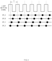
- FIG. 3 is a conceptual diagram illustrating a representation of an example of operations of a sampling phase calibration circuit 200.
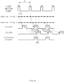
- FIG. 4 is a conceptual diagram illustrating a representation of an example of operations of a delay calibration circuit 300.
- FIG. 5 is a conceptual diagram illustrating a representation of an example of operations of a sensitivity calibration circuit 400.
- the image synchronization device 10 may include a light emitting source 100, a sampling phase calibration circuit 200, a delay calibration circuit 300, and a sensitivity calibration circuit 400.
- the light emitting source 100 may periodically emit light at intervals of a predetermined time.
- the light emitting source 100 may be a device (e.g., a lamp, a light emitting diode (LED), a laser diode, etc.) for converting electric energy into light energy.
- the light emitting source 100 may also be implemented as any one of devices capable of transmitting light energy to the image sensor SENSOR1 or SENSOR2.
- the light emitting source 100 need not always be implemented as a separate device. For example, natural light may also be used as the light emitting source 100. Referring to FIG.
- the first image information (IM1) including image frames (IF11 ⁇ IF16) may have a value of "101010”
- the second image information (IM2) including image frames (IF21 ⁇ IF26) may also have the value of "101010” in order of time in the same manner as in the first image information (IM1).
Landscapes
- Engineering & Computer Science (AREA)
- Multimedia (AREA)
- Signal Processing (AREA)
- Health & Medical Sciences (AREA)
- Biomedical Technology (AREA)
- General Health & Medical Sciences (AREA)
- Human Computer Interaction (AREA)
- Studio Devices (AREA)
Claims (12)
- Eine Bildsynchronisationsvorrichtung zum Synchronisieren von Bildinformation, die von einer Mehrzahl von Bildsensoren erzeugt wird, wobei die Vorrichtung aufweist:eine lichtemittierende Quelle (100), die konfiguriert ist, um Licht mit einer vorbestimmten lichtemittierenden Phase zu emittieren; undeinen Abtastphasenkalibrierungsschaltkreis (200), der konfiguriert ist, um eine erste Abtastphase eines ersten Bildsensors (SENSOR1) und eine zweite Abtastphase eines zweiten Bildsensors (SENSOR2) mit der lichtemittierenden Phase der lichtemittierenden Quelle zu synchronisieren, wobei der Abtastphasenkalibrierungsschaltkreis (200) enthält:einen Periodeneinstellschaltkreis (210a, 210b), der konfiguriert ist, um eine lichtemittierende Periode der lichtemittierenden Quelle (100) einzustellen, um identisch zu einer Abtastperiode des ersten Bildsensors (SENSOR1) und des zweiten Bildsensors (SENSOR2) zu sein;gekennzeichnet durch:einen Abtastphaseninformationserzeugungsschaltkreis (220a, 220b), der konfiguriert ist, um die erste Abtastphase in einer Weise zu kalibrieren, dass der erste Bildsensor (SENSOR1) ein Erfassen und Abtasten eines lichtemittierenden Signals der lichtemittierenden Quelle (100) bei unterschiedlichen Abtastphasen (SP_A, SP_B, SP_C, SP_D) durchführt, um eine erste Abtastphaseninformation für jede der unterschiedlichen Abtastphasen zu erzeugen, und konfiguriert ist, um die zweite Abtastphase in einer Weise zu kalibrieren, dass der zweite Bildsensor (SENSOR2) ein Erfassen und Abtasten des lichtemittierenden Signals bei den unterschiedlichen Abtastphasen durchführt, um eine zweite Abtastphaseninformation für jede der unterschiedlichen Abtastphasen zu erzeugen; undeinen Abtastphasenentscheidungsschaltkreis (230a, 230b), der konfiguriert ist, um eine der unterschiedlichen Abtastphasen als die erste Abtastphase basierend auf der ersten Abtastphaseninformation zu bestimmen und um eine der unterschiedlichen Abtastphasen als die zweite Abtastphase basierend auf der zweiten Abtastphaseninformation zu bestimmen.
- Die Bildsynchronisationsvorrichtung gemäß Anspruch 1, wobei der Abtastphaseninformationserzeugungsschaltkreis (220a, 220b) die erste Abtastphase und die zweite Abtastphase sequentiell erhöht oder verringert.
- Die Bildsynchronisationsvorrichtung gemäß Anspruch 1, ferner aufweisend:
einen Verzögerungskalibrierungsschaltkreis (300), der konfiguriert ist, um eine Verzögerungsinformation durch Vergleichen einer ersten Bildinformation, die von dem ersten Bildsensor übertragen wird, und einer zweiten Bildinformation, die von dem zweiten Bildsensor übertragen wird, nach dem Empfangen eines Verzögerungskalibrierungsbetriebsstartsignals von dem Abtastphasenkalibrierungsschaltkreis (200) zu detektieren und eine Verzögerung der ersten Bildinformation und der zweiten Bildinformation basierend auf der Verzögerungsinformation zu kalibrieren, wobei die erste Bildinformation und die zweite Bildinformation von dem ersten Bildsensor (SENSOR1) beziehungsweise dem zweiten Bildsensor (SENSOR2) erhalten werden, wenn der erste Bildsensor (SENSOR1) und der zweite Bildsensor (SENSOR2) ein Erfassen und Abtasten des lichtemittierenden Signals der lichtemittierenden Quelle (100) durchführen. - Die Bildsynchronisationsvorrichtung gemäß Anspruch 3, wobei der Verzögerungskalibrierungsschaltkreis (300) aufweist:einen lichtemittierenden Periodenkalibrierungsschaltkreis (310), der konfiguriert ist, um eine lichtemittierende Periode der lichtemittierenden Quelle (100) zu kalibrieren; undeinen Verzögerungsinformationsdetektionsschaltkreis (320), der konfiguriert ist, um eine Verzögerungsinformation basierend auf einem Ergebnis eines Vergleichs zwischen einer ersten lichtemittierenden Periodeninformation und einer zweiten lichtemittierenden Periodeninformation zu detektieren, wobei die erste lichtemittierende Periodeninformation erzeugt wird, wenn der erste Bildsensor (SENSOR1) ein Erfassen und Abtasten eines lichtemittierenden Signals der lichtemittierenden Quelle, die bei der kalibrierten lichtemittierenden Periode arbeitet, durchführt, und die zweite lichtemittierende Periodeninformation erzeugt wird, wenn der zweite Bildsensor (SENSOR2) ein Erfassen und Abtasten eines lichtemittierenden Signals der lichtemittierenden Quelle, die bei der kalibrierten lichtemittierenden Periode arbeitet, durchführt.
- Die Bildsynchronisationsvorrichtung gemäß Anspruch 3, wobei der Verzögerungskalibrierungsschaltkreis (300) aufweist:einen lichtemittierenden Periodenkalibrierungsschaltkreis (310), der konfiguriert ist, um die Abtastperiode von jedem des ersten Bildsensors (SENSOR1) und des zweiten Bildsensors (SENSOR2) zu kalibrieren;einen Verzögerungsinformationsdetektionsschaltkreis (320), der konfiguriert ist, um eine Verzögerungsinformation basierend auf einem Ergebnis eines Vergleichs zwischen einer ersten Abtastperiodeninformation, die von dem ersten Bildsensor empfangen wird, und einer zweiten Abtastperiodeninformation, die von dem zweiten Bildsensor empfangen wird, zu detektieren, wobei jeder des ersten und des zweiten Bildsensors bei der kalibrierten Abtastperiode arbeitet.
- Die Bildsynchronisationsvorrichtung gemäß Anspruch 4, wobei die Abtastperiode des ersten Bildsensors (SENSOR1) identisch zu der Abtastperiode des zweiten Bildsensors (SENSOR2) ist.
- Die Bildsynchronisationsvorrichtung gemäß Anspruch 4, ferner aufweisend:
einen Entscheidungsschaltkreis (330), der konfiguriert ist, um zu entscheiden, ob der Verzögerungskalibrierungsschaltkreis (300) fortfährt, einen Verzögerungskalibrierungsbetrieb durchzuführen, nachdem der Verzögerungsinformationsdetektionsschaltkreis (320) die Verzögerungsinformation detektiert. - Die Bildsynchronisationsvorrichtung gemäß Anspruch 7, wobei der Entscheidungsschaltkreis (330) ein Abtastperiodenkalibrierungsfortsetzungssignal basierend auf der Verzögerungsinformation erzeugt.
- Die Bildsynchronisationsvorrichtung gemäß Anspruch 7, wobei der lichtemittierende Periodenkalibrierungsschaltkreis (310) die lichtemittierende Periode der lichtemittierenden Quelle so kalibriert, dass sie sich von einer vorherigen lichtemittierenden Periode unterscheidet, basierend auf dem Abtastperiodenkalibrierungsfortsetzungssignal.
- Die Bildsynchronisationsvorrichtung gemäß Anspruch 7, wobei der Verzögerungsinformationsdetektionsschaltkreis (320) eine Verzögerung der ersten lichtemittierenden Periodeninformation und eine Verzögerung der zweiten lichtemittierenden Periodeninformation basierend auf der Verzögerungsinformation kalibriert.
- Die Bildsynchronisationsvorrichtung gemäß Anspruch 10, wobei:
wenn der Entscheidungsschaltkreis (330) entscheidet, fortzufahren, den Verzögerungskalibrierungsbetrieb durchzuführen, der Verzögerungsinformationsdetektionsschaltkreis (320) eine temporäre Verzögerungsinformation durch Vergleichen der ersten lichtemittierenden Periodeninformation, die eine kalibrierte Verzögerung hat, mit der zweiten lichtemittierenden Periodeninformation, die eine kalibrierte Verzögerung hat, erzeugt und eine vorherige Verzögerungsinformation auf eine Summe der vorherigen Verzögerungsinformation und der temporären Verzögerungsinformation aktualisiert. - Die Bildsynchronisationsvorrichtung gemäß Anspruch 1, ferner aufweisend:
einen Empfindlichkeitskalibrierungsschaltkreis (400), der konfiguriert ist, um eine Skalierung oder eine Versatzeinstellung von zumindest einer der ersten Bildinformation und der zweiten Bildinformation in einer solchen Weise durchzuführen, dass ein maximaler Pegel eines Pulses, der der ersten Bildinformation entspricht, identisch zu einem maximalen Pegel eines Pulses ist, der der zweiten Bildinformation entspricht.
Applications Claiming Priority (2)
| Application Number | Priority Date | Filing Date | Title |
|---|---|---|---|
| KR1020170146479A KR20190051146A (ko) | 2017-11-06 | 2017-11-06 | 이미지 동기화 장치 및 이를 포함하는 이미지 정보 생성 장치 |
| PCT/KR2018/006691 WO2019088389A1 (ko) | 2017-11-06 | 2018-06-14 | 이미지 동기화 장치 및 이를 포함하는 이미지 정보 생성 장치 |
Publications (3)
| Publication Number | Publication Date |
|---|---|
| EP3709630A1 EP3709630A1 (de) | 2020-09-16 |
| EP3709630A4 EP3709630A4 (de) | 2021-06-23 |
| EP3709630B1 true EP3709630B1 (de) | 2025-03-19 |
Family
ID=66332072
Family Applications (1)
| Application Number | Title | Priority Date | Filing Date |
|---|---|---|---|
| EP18873550.0A Active EP3709630B1 (de) | 2017-11-06 | 2018-06-14 | Bildsynchronisierungsvorrichtung und diese aufweisende bildinformationen erzeugende vorrichtung |
Country Status (4)
| Country | Link |
|---|---|
| US (1) | US11483505B2 (de) |
| EP (1) | EP3709630B1 (de) |
| KR (1) | KR20190051146A (de) |
| WO (1) | WO2019088389A1 (de) |
Families Citing this family (2)
| Publication number | Priority date | Publication date | Assignee | Title |
|---|---|---|---|---|
| US11592832B2 (en) * | 2018-08-20 | 2023-02-28 | Uatc, Llc | Automatic robotically steered camera for targeted high performance perception and vehicle control |
| WO2021070426A1 (ja) * | 2019-10-09 | 2021-04-15 | ソニーセミコンダクタソリューションズ株式会社 | 撮像回路および撮像装置 |
Citations (3)
| Publication number | Priority date | Publication date | Assignee | Title |
|---|---|---|---|---|
| JP2008252401A (ja) * | 2007-03-29 | 2008-10-16 | Fujifilm Corp | 撮像システム、撮像方法、および撮像プログラム |
| JP2012124574A (ja) * | 2010-12-06 | 2012-06-28 | Toshiba Corp | ネットワークカメラシステムおよびこれに利用する映像情報時刻同期方法 |
| WO2015142412A2 (en) * | 2014-03-20 | 2015-09-24 | Gopro, Inc. | Auto-alignment of image sensors in a multi-camera system |
Family Cites Families (11)
| Publication number | Priority date | Publication date | Assignee | Title |
|---|---|---|---|---|
| KR101678691B1 (ko) | 2010-05-12 | 2016-11-23 | 삼성전자주식회사 | 광원의 특성을 이용한 이미지 처리 장치 및 방법 |
| JP5870510B2 (ja) | 2010-09-14 | 2016-03-01 | 株式会社リコー | ステレオカメラ装置、校正方法およびプログラム |
| US10489912B1 (en) * | 2013-12-20 | 2019-11-26 | Amazon Technologies, Inc. | Automated rectification of stereo cameras |
| US20170041591A1 (en) * | 2013-12-25 | 2017-02-09 | Hitachi Automotive Systems ,Ltd. | Vehicle-Mounted Image Recognition Device |
| KR102160120B1 (ko) | 2014-03-14 | 2020-09-25 | 삼성전자주식회사 | 샘플링 주기를 제어할 수 있는 샘플링 주기 제어 회로 |
| US8988509B1 (en) * | 2014-03-20 | 2015-03-24 | Gopro, Inc. | Auto-alignment of image sensors in a multi-camera system |
| JP6095634B2 (ja) | 2014-11-25 | 2017-03-15 | 京セラドキュメントソリューションズ株式会社 | 画像読取装置、画像形成装置、画像読取方法 |
| KR102523301B1 (ko) | 2015-12-15 | 2023-04-19 | 삼성전자주식회사 | 플리커를 제거하는 이미지 센서 회로 및 이를 포함하는 카메라 장치 |
| JP6766071B2 (ja) * | 2015-12-21 | 2020-10-07 | 株式会社小糸製作所 | 車両用画像取得装置およびそれを備えた車両 |
| US9930320B2 (en) * | 2016-05-04 | 2018-03-27 | Apple Inc. | Resolving three dimensional spatial information using time-shared structured lighting that embeds digital communication |
| KR102385333B1 (ko) * | 2017-09-15 | 2022-04-12 | 삼성전자주식회사 | 복수의 이미지 센서들을 제어하기 위한 전자 장치 및 방법 |
-
2017
- 2017-11-06 KR KR1020170146479A patent/KR20190051146A/ko not_active Withdrawn
-
2018
- 2018-06-14 US US16/769,830 patent/US11483505B2/en active Active
- 2018-06-14 WO PCT/KR2018/006691 patent/WO2019088389A1/ko not_active Ceased
- 2018-06-14 EP EP18873550.0A patent/EP3709630B1/de active Active
Patent Citations (3)
| Publication number | Priority date | Publication date | Assignee | Title |
|---|---|---|---|---|
| JP2008252401A (ja) * | 2007-03-29 | 2008-10-16 | Fujifilm Corp | 撮像システム、撮像方法、および撮像プログラム |
| JP2012124574A (ja) * | 2010-12-06 | 2012-06-28 | Toshiba Corp | ネットワークカメラシステムおよびこれに利用する映像情報時刻同期方法 |
| WO2015142412A2 (en) * | 2014-03-20 | 2015-09-24 | Gopro, Inc. | Auto-alignment of image sensors in a multi-camera system |
Also Published As
| Publication number | Publication date |
|---|---|
| EP3709630A1 (de) | 2020-09-16 |
| WO2019088389A1 (ko) | 2019-05-09 |
| US20210377483A1 (en) | 2021-12-02 |
| KR20190051146A (ko) | 2019-05-15 |
| EP3709630A4 (de) | 2021-06-23 |
| US11483505B2 (en) | 2022-10-25 |
Similar Documents
| Publication | Publication Date | Title |
|---|---|---|
| EP3550330B1 (de) | Entfernungsmessvorrichtung | |
| KR102136850B1 (ko) | 깊이 센서, 및 이의 동작 방법 | |
| US11109016B2 (en) | Methods and apparatus for error detection in an imaging system | |
| JP2018136123A (ja) | 距離センサ及びユーザインタフェース装置 | |
| US9894300B2 (en) | Image sensing device for measuring temperature without temperature sensor and method for driving the same | |
| WO2020095603A1 (ja) | 投光制御装置、投光制御方法 | |
| KR20100128797A (ko) | 거리 센서, 3차원 이미지 센서 및 그 거리 산출 방법 | |
| JP5064197B2 (ja) | 光電センサ | |
| US20130011130A1 (en) | Shutter control device | |
| EP3432572B1 (de) | Bilderfassungszubehör, bilderfassungsvorrichtung, steuerungsverfahren dafür und kommunikationssteuerungsprogramm | |
| EP3709630A1 (de) | Bildsynchronisierungsvorrichtung und diese aufweisende bildinformationen erzeugende vorrichtung | |
| FR2530095A1 (fr) | Circuit de synchronisation pour decodeur viterbi | |
| WO2012111196A1 (ja) | 物体検知システム | |
| JP2021517256A (ja) | マルチカメラ環境向けに最適化された飛行時間測定ビジョンカメラ | |
| KR20180056540A (ko) | 프레임 그래버, 이를 포함하는 영상 처리 시스템, 및 프레임 그래버를 이용한 영상 처리 방법 | |
| CN104796613A (zh) | 影像系统 | |
| US9459351B2 (en) | Image system | |
| US20130176426A1 (en) | Image sensor, method of sensing image, and image capturing apparatus including the image sensor | |
| JP2014202614A (ja) | 赤外線検知装置および検知対象の検知方法 | |
| JP2017188838A (ja) | 画像処理装置、その制御方法及びプログラム | |
| JP2015507831A (ja) | 符号化された光源を検出し、制御する方法 | |
| JP2019095216A (ja) | 距離画像センサおよびそのキャリブレーション方法 | |
| JP2014239303A (ja) | 無線撮像システム、無線撮像システムの制御方法、プログラムおよび無線通信装置 | |
| KR101924152B1 (ko) | 자외선 검출 장치, 자외선 검출 방법, 및 자외선 측정 애플리케이션을 포함하는 컴퓨터 판독 가능 매체 | |
| JP2002368595A (ja) | 放射パルス介在型センサ |
Legal Events
| Date | Code | Title | Description |
|---|---|---|---|
| STAA | Information on the status of an ep patent application or granted ep patent |
Free format text: STATUS: THE INTERNATIONAL PUBLICATION HAS BEEN MADE |
|
| PUAI | Public reference made under article 153(3) epc to a published international application that has entered the european phase |
Free format text: ORIGINAL CODE: 0009012 |
|
| STAA | Information on the status of an ep patent application or granted ep patent |
Free format text: STATUS: REQUEST FOR EXAMINATION WAS MADE |
|
| 17P | Request for examination filed |
Effective date: 20200527 |
|
| AK | Designated contracting states |
Kind code of ref document: A1 Designated state(s): AL AT BE BG CH CY CZ DE DK EE ES FI FR GB GR HR HU IE IS IT LI LT LU LV MC MK MT NL NO PL PT RO RS SE SI SK SM TR |
|
| AX | Request for extension of the european patent |
Extension state: BA ME |
|
| DAV | Request for validation of the european patent (deleted) | ||
| DAX | Request for extension of the european patent (deleted) | ||
| A4 | Supplementary search report drawn up and despatched |
Effective date: 20210527 |
|
| RIC1 | Information provided on ipc code assigned before grant |
Ipc: H04N 5/341 20110101AFI20210520BHEP Ipc: H04N 5/225 20060101ALI20210520BHEP Ipc: H04N 5/247 20060101ALI20210520BHEP Ipc: H04N 5/04 20060101ALI20210520BHEP Ipc: H04N 17/00 20060101ALI20210520BHEP |
|
| RIC1 | Information provided on ipc code assigned before grant |
Ipc: H04N 5/341 20110101AFI20210611BHEP Ipc: H04N 5/225 20060101ALI20210611BHEP Ipc: H04N 5/247 20060101ALI20210611BHEP Ipc: H04N 5/04 20060101ALI20210611BHEP Ipc: H04N 17/00 20060101ALI20210611BHEP |
|
| STAA | Information on the status of an ep patent application or granted ep patent |
Free format text: STATUS: EXAMINATION IS IN PROGRESS |
|
| 17Q | First examination report despatched |
Effective date: 20230517 |
|
| REG | Reference to a national code |
Ipc: H04N0023450000 Ref country code: DE Ref legal event code: R079 Ref document number: 602018080349 Country of ref document: DE Free format text: PREVIOUS MAIN CLASS: H04N0005341000 |
|
| GRAP | Despatch of communication of intention to grant a patent |
Free format text: ORIGINAL CODE: EPIDOSNIGR1 |
|
| STAA | Information on the status of an ep patent application or granted ep patent |
Free format text: STATUS: GRANT OF PATENT IS INTENDED |
|
| RIC1 | Information provided on ipc code assigned before grant |
Ipc: H04N 25/76 20230101ALI20241003BHEP Ipc: H04N 5/04 20060101ALI20241003BHEP Ipc: H04N 17/00 20060101ALI20241003BHEP Ipc: H04N 23/76 20230101ALI20241003BHEP Ipc: H04N 23/90 20230101ALI20241003BHEP Ipc: H04N 23/45 20230101AFI20241003BHEP |
|
| INTG | Intention to grant announced |
Effective date: 20241018 |
|
| RIN1 | Information on inventor provided before grant (corrected) |
Inventor name: JEONG, CHUN SEOK Inventor name: LEE, JAE JIN Inventor name: LEE, SEUNG HUN Inventor name: LEE, DOO BOCK Inventor name: ROH, WAN JUN Inventor name: KIM, CHANG HYUN |
|
| GRAS | Grant fee paid |
Free format text: ORIGINAL CODE: EPIDOSNIGR3 |
|
| GRAA | (expected) grant |
Free format text: ORIGINAL CODE: 0009210 |
|
| STAA | Information on the status of an ep patent application or granted ep patent |
Free format text: STATUS: THE PATENT HAS BEEN GRANTED |
|
| AK | Designated contracting states |
Kind code of ref document: B1 Designated state(s): AL AT BE BG CH CY CZ DE DK EE ES FI FR GB GR HR HU IE IS IT LI LT LU LV MC MK MT NL NO PL PT RO RS SE SI SK SM TR |
|
| REG | Reference to a national code |
Ref country code: GB Ref legal event code: FG4D |
|
| REG | Reference to a national code |
Ref country code: CH Ref legal event code: EP |
|
| REG | Reference to a national code |
Ref country code: DE Ref legal event code: R096 Ref document number: 602018080349 Country of ref document: DE |
|
| REG | Reference to a national code |
Ref country code: IE Ref legal event code: FG4D |
|
| P01 | Opt-out of the competence of the unified patent court (upc) registered |
Free format text: CASE NUMBER: APP_18327/2025 Effective date: 20250415 |
|
| PG25 | Lapsed in a contracting state [announced via postgrant information from national office to epo] |
Ref country code: RS Free format text: LAPSE BECAUSE OF FAILURE TO SUBMIT A TRANSLATION OF THE DESCRIPTION OR TO PAY THE FEE WITHIN THE PRESCRIBED TIME-LIMIT Effective date: 20250619 |
|
| PG25 | Lapsed in a contracting state [announced via postgrant information from national office to epo] |
Ref country code: FI Free format text: LAPSE BECAUSE OF FAILURE TO SUBMIT A TRANSLATION OF THE DESCRIPTION OR TO PAY THE FEE WITHIN THE PRESCRIBED TIME-LIMIT Effective date: 20250319 |
|
| PGFP | Annual fee paid to national office [announced via postgrant information from national office to epo] |
Ref country code: DE Payment date: 20250515 Year of fee payment: 8 |
|
| REG | Reference to a national code |
Ref country code: LT Ref legal event code: MG9D |
|
| PG25 | Lapsed in a contracting state [announced via postgrant information from national office to epo] |
Ref country code: NO Free format text: LAPSE BECAUSE OF FAILURE TO SUBMIT A TRANSLATION OF THE DESCRIPTION OR TO PAY THE FEE WITHIN THE PRESCRIBED TIME-LIMIT Effective date: 20250619 |
|
| PG25 | Lapsed in a contracting state [announced via postgrant information from national office to epo] |
Ref country code: HR Free format text: LAPSE BECAUSE OF FAILURE TO SUBMIT A TRANSLATION OF THE DESCRIPTION OR TO PAY THE FEE WITHIN THE PRESCRIBED TIME-LIMIT Effective date: 20250319 |
|
| PG25 | Lapsed in a contracting state [announced via postgrant information from national office to epo] |
Ref country code: LV Free format text: LAPSE BECAUSE OF FAILURE TO SUBMIT A TRANSLATION OF THE DESCRIPTION OR TO PAY THE FEE WITHIN THE PRESCRIBED TIME-LIMIT Effective date: 20250319 |
|
| PG25 | Lapsed in a contracting state [announced via postgrant information from national office to epo] |
Ref country code: GR Free format text: LAPSE BECAUSE OF FAILURE TO SUBMIT A TRANSLATION OF THE DESCRIPTION OR TO PAY THE FEE WITHIN THE PRESCRIBED TIME-LIMIT Effective date: 20250620 Ref country code: BG Free format text: LAPSE BECAUSE OF FAILURE TO SUBMIT A TRANSLATION OF THE DESCRIPTION OR TO PAY THE FEE WITHIN THE PRESCRIBED TIME-LIMIT Effective date: 20250319 |
|
| REG | Reference to a national code |
Ref country code: NL Ref legal event code: MP Effective date: 20250319 |
|
| REG | Reference to a national code |
Ref country code: AT Ref legal event code: MK05 Ref document number: 1777948 Country of ref document: AT Kind code of ref document: T Effective date: 20250319 |
|
| PG25 | Lapsed in a contracting state [announced via postgrant information from national office to epo] |
Ref country code: NL Free format text: LAPSE BECAUSE OF FAILURE TO SUBMIT A TRANSLATION OF THE DESCRIPTION OR TO PAY THE FEE WITHIN THE PRESCRIBED TIME-LIMIT Effective date: 20250319 |
|
| PG25 | Lapsed in a contracting state [announced via postgrant information from national office to epo] |
Ref country code: SE Free format text: LAPSE BECAUSE OF FAILURE TO SUBMIT A TRANSLATION OF THE DESCRIPTION OR TO PAY THE FEE WITHIN THE PRESCRIBED TIME-LIMIT Effective date: 20250319 |
|
| PG25 | Lapsed in a contracting state [announced via postgrant information from national office to epo] |
Ref country code: SM Free format text: LAPSE BECAUSE OF FAILURE TO SUBMIT A TRANSLATION OF THE DESCRIPTION OR TO PAY THE FEE WITHIN THE PRESCRIBED TIME-LIMIT Effective date: 20250319 |
|
| PG25 | Lapsed in a contracting state [announced via postgrant information from national office to epo] |
Ref country code: ES Free format text: LAPSE BECAUSE OF FAILURE TO SUBMIT A TRANSLATION OF THE DESCRIPTION OR TO PAY THE FEE WITHIN THE PRESCRIBED TIME-LIMIT Effective date: 20250319 Ref country code: PT Free format text: LAPSE BECAUSE OF FAILURE TO SUBMIT A TRANSLATION OF THE DESCRIPTION OR TO PAY THE FEE WITHIN THE PRESCRIBED TIME-LIMIT Effective date: 20250721 |
|
| PG25 | Lapsed in a contracting state [announced via postgrant information from national office to epo] |
Ref country code: PL Free format text: LAPSE BECAUSE OF FAILURE TO SUBMIT A TRANSLATION OF THE DESCRIPTION OR TO PAY THE FEE WITHIN THE PRESCRIBED TIME-LIMIT Effective date: 20250319 Ref country code: IT Free format text: LAPSE BECAUSE OF FAILURE TO SUBMIT A TRANSLATION OF THE DESCRIPTION OR TO PAY THE FEE WITHIN THE PRESCRIBED TIME-LIMIT Effective date: 20250319 |
|
| PG25 | Lapsed in a contracting state [announced via postgrant information from national office to epo] |
Ref country code: AT Free format text: LAPSE BECAUSE OF FAILURE TO SUBMIT A TRANSLATION OF THE DESCRIPTION OR TO PAY THE FEE WITHIN THE PRESCRIBED TIME-LIMIT Effective date: 20250319 |
|
| PG25 | Lapsed in a contracting state [announced via postgrant information from national office to epo] |
Ref country code: EE Free format text: LAPSE BECAUSE OF FAILURE TO SUBMIT A TRANSLATION OF THE DESCRIPTION OR TO PAY THE FEE WITHIN THE PRESCRIBED TIME-LIMIT Effective date: 20250319 Ref country code: CZ Free format text: LAPSE BECAUSE OF FAILURE TO SUBMIT A TRANSLATION OF THE DESCRIPTION OR TO PAY THE FEE WITHIN THE PRESCRIBED TIME-LIMIT Effective date: 20250319 |
|
| PG25 | Lapsed in a contracting state [announced via postgrant information from national office to epo] |
Ref country code: RO Free format text: LAPSE BECAUSE OF FAILURE TO SUBMIT A TRANSLATION OF THE DESCRIPTION OR TO PAY THE FEE WITHIN THE PRESCRIBED TIME-LIMIT Effective date: 20250319 |
|
| PG25 | Lapsed in a contracting state [announced via postgrant information from national office to epo] |
Ref country code: SK Free format text: LAPSE BECAUSE OF FAILURE TO SUBMIT A TRANSLATION OF THE DESCRIPTION OR TO PAY THE FEE WITHIN THE PRESCRIBED TIME-LIMIT Effective date: 20250319 |
|
| PG25 | Lapsed in a contracting state [announced via postgrant information from national office to epo] |
Ref country code: IS Free format text: LAPSE BECAUSE OF FAILURE TO SUBMIT A TRANSLATION OF THE DESCRIPTION OR TO PAY THE FEE WITHIN THE PRESCRIBED TIME-LIMIT Effective date: 20250719 |
|
| REG | Reference to a national code |
Ref country code: DE Ref legal event code: R097 Ref document number: 602018080349 Country of ref document: DE |
|
| PG25 | Lapsed in a contracting state [announced via postgrant information from national office to epo] |
Ref country code: DK Free format text: LAPSE BECAUSE OF FAILURE TO SUBMIT A TRANSLATION OF THE DESCRIPTION OR TO PAY THE FEE WITHIN THE PRESCRIBED TIME-LIMIT Effective date: 20250319 |
|
| PLBE | No opposition filed within time limit |
Free format text: ORIGINAL CODE: 0009261 |
|
| STAA | Information on the status of an ep patent application or granted ep patent |
Free format text: STATUS: NO OPPOSITION FILED WITHIN TIME LIMIT |
|
| REG | Reference to a national code |
Ref country code: CH Ref legal event code: H13 Free format text: ST27 STATUS EVENT CODE: U-0-0-H10-H13 (AS PROVIDED BY THE NATIONAL OFFICE) Effective date: 20260127 |
|
| REG | Reference to a national code |
Ref country code: CH Ref legal event code: L10 Free format text: ST27 STATUS EVENT CODE: U-0-0-L10-L00 (AS PROVIDED BY THE NATIONAL OFFICE) Effective date: 20260128 |
|
| PG25 | Lapsed in a contracting state [announced via postgrant information from national office to epo] |
Ref country code: MC Free format text: LAPSE BECAUSE OF FAILURE TO SUBMIT A TRANSLATION OF THE DESCRIPTION OR TO PAY THE FEE WITHIN THE PRESCRIBED TIME-LIMIT Effective date: 20250319 |
|
| PG25 | Lapsed in a contracting state [announced via postgrant information from national office to epo] |
Ref country code: LU Free format text: LAPSE BECAUSE OF NON-PAYMENT OF DUE FEES Effective date: 20250614 |
|
| 26N | No opposition filed |
Effective date: 20251222 |
|
| GBPC | Gb: european patent ceased through non-payment of renewal fee |
Effective date: 20250619 |
|
| REG | Reference to a national code |
Ref country code: BE Ref legal event code: MM Effective date: 20250630 |
|
| PG25 | Lapsed in a contracting state [announced via postgrant information from national office to epo] |
Ref country code: GB Free format text: LAPSE BECAUSE OF NON-PAYMENT OF DUE FEES Effective date: 20250619 |
|
| PG25 | Lapsed in a contracting state [announced via postgrant information from national office to epo] |
Ref country code: IE Free format text: LAPSE BECAUSE OF NON-PAYMENT OF DUE FEES Effective date: 20250614 |
|
| PG25 | Lapsed in a contracting state [announced via postgrant information from national office to epo] |
Ref country code: BE Free format text: LAPSE BECAUSE OF NON-PAYMENT OF DUE FEES Effective date: 20250630 |
|
| PG25 | Lapsed in a contracting state [announced via postgrant information from national office to epo] |
Ref country code: FR Free format text: LAPSE BECAUSE OF NON-PAYMENT OF DUE FEES Effective date: 20250630 |
|
| PG25 | Lapsed in a contracting state [announced via postgrant information from national office to epo] |
Ref country code: CH Free format text: LAPSE BECAUSE OF NON-PAYMENT OF DUE FEES Effective date: 20250630 |