EP3709593B1 - Data distribution method and related apparatuses - Google Patents
Data distribution method and related apparatuses Download PDFInfo
- Publication number
- EP3709593B1 EP3709593B1 EP19209926.5A EP19209926A EP3709593B1 EP 3709593 B1 EP3709593 B1 EP 3709593B1 EP 19209926 A EP19209926 A EP 19209926A EP 3709593 B1 EP3709593 B1 EP 3709593B1
- Authority
- EP
- European Patent Office
- Prior art keywords
- circuit
- circuits
- stream
- data
- physical layer
- Prior art date
- Legal status (The legal status is an assumption and is not a legal conclusion. Google has not performed a legal analysis and makes no representation as to the accuracy of the status listed.)
- Active
Links
- 238000000034 method Methods 0.000 title claims description 120
- 239000003550 marker Substances 0.000 claims description 224
- 238000012545 processing Methods 0.000 claims description 151
- 238000003780 insertion Methods 0.000 claims description 62
- 230000037431 insertion Effects 0.000 claims description 62
- 230000008569 process Effects 0.000 claims description 56
- 238000004590 computer program Methods 0.000 claims 1
- 238000010586 diagram Methods 0.000 description 34
- 230000002776 aggregation Effects 0.000 description 21
- 238000004220 aggregation Methods 0.000 description 21
- 230000007246 mechanism Effects 0.000 description 12
- 230000003287 optical effect Effects 0.000 description 11
- 230000006855 networking Effects 0.000 description 10
- 230000004931 aggregating effect Effects 0.000 description 9
- 230000005540 biological transmission Effects 0.000 description 5
- 238000004891 communication Methods 0.000 description 5
- 238000005516 engineering process Methods 0.000 description 5
- 238000005265 energy consumption Methods 0.000 description 4
- 238000007781 pre-processing Methods 0.000 description 4
- 230000009471 action Effects 0.000 description 3
- 230000000903 blocking effect Effects 0.000 description 3
- 230000008878 coupling Effects 0.000 description 3
- 238000010168 coupling process Methods 0.000 description 3
- 238000005859 coupling reaction Methods 0.000 description 3
- 238000012546 transfer Methods 0.000 description 3
- 230000008859 change Effects 0.000 description 2
- 230000003993 interaction Effects 0.000 description 2
- 238000011161 development Methods 0.000 description 1
- 230000006870 function Effects 0.000 description 1
- 238000012986 modification Methods 0.000 description 1
- 230000004048 modification Effects 0.000 description 1
- VLCQZHSMCYCDJL-UHFFFAOYSA-N tribenuron methyl Chemical compound COC(=O)C1=CC=CC=C1S(=O)(=O)NC(=O)N(C)C1=NC(C)=NC(OC)=N1 VLCQZHSMCYCDJL-UHFFFAOYSA-N 0.000 description 1
Images


Classifications
-
- H—ELECTRICITY
- H04—ELECTRIC COMMUNICATION TECHNIQUE
- H04L—TRANSMISSION OF DIGITAL INFORMATION, e.g. TELEGRAPHIC COMMUNICATION
- H04L45/00—Routing or path finding of packets in data switching networks
- H04L45/24—Multipath
- H04L45/245—Link aggregation, e.g. trunking
-
- H—ELECTRICITY
- H03—ELECTRONIC CIRCUITRY
- H03M—CODING; DECODING; CODE CONVERSION IN GENERAL
- H03M9/00—Parallel/series conversion or vice versa
-
- H—ELECTRICITY
- H04—ELECTRIC COMMUNICATION TECHNIQUE
- H04L—TRANSMISSION OF DIGITAL INFORMATION, e.g. TELEGRAPHIC COMMUNICATION
- H04L1/00—Arrangements for detecting or preventing errors in the information received
- H04L1/004—Arrangements for detecting or preventing errors in the information received by using forward error control
- H04L1/0041—Arrangements at the transmitter end
- H04L1/0043—Realisations of complexity reduction techniques, e.g. use of look-up tables
-
- H—ELECTRICITY
- H04—ELECTRIC COMMUNICATION TECHNIQUE
- H04L—TRANSMISSION OF DIGITAL INFORMATION, e.g. TELEGRAPHIC COMMUNICATION
- H04L1/00—Arrangements for detecting or preventing errors in the information received
- H04L1/004—Arrangements for detecting or preventing errors in the information received by using forward error control
- H04L1/0045—Arrangements at the receiver end
- H04L1/0052—Realisations of complexity reduction techniques, e.g. pipelining or use of look-up tables
-
- H—ELECTRICITY
- H04—ELECTRIC COMMUNICATION TECHNIQUE
- H04L—TRANSMISSION OF DIGITAL INFORMATION, e.g. TELEGRAPHIC COMMUNICATION
- H04L1/00—Arrangements for detecting or preventing errors in the information received
- H04L1/004—Arrangements for detecting or preventing errors in the information received by using forward error control
- H04L1/0056—Systems characterized by the type of code used
- H04L1/0067—Rate matching
-
- H—ELECTRICITY
- H04—ELECTRIC COMMUNICATION TECHNIQUE
- H04L—TRANSMISSION OF DIGITAL INFORMATION, e.g. TELEGRAPHIC COMMUNICATION
- H04L25/00—Baseband systems
- H04L25/02—Details ; arrangements for supplying electrical power along data transmission lines
- H04L25/03—Shaping networks in transmitter or receiver, e.g. adaptive shaping networks
- H04L25/03828—Arrangements for spectral shaping; Arrangements for providing signals with specified spectral properties
- H04L25/03866—Arrangements for spectral shaping; Arrangements for providing signals with specified spectral properties using scrambling
-
- H—ELECTRICITY
- H04—ELECTRIC COMMUNICATION TECHNIQUE
- H04L—TRANSMISSION OF DIGITAL INFORMATION, e.g. TELEGRAPHIC COMMUNICATION
- H04L25/00—Baseband systems
- H04L25/02—Details ; arrangements for supplying electrical power along data transmission lines
- H04L25/14—Channel dividing arrangements, i.e. in which a single bit stream is divided between several baseband channels and reassembled at the receiver
-
- H—ELECTRICITY
- H04—ELECTRIC COMMUNICATION TECHNIQUE
- H04L—TRANSMISSION OF DIGITAL INFORMATION, e.g. TELEGRAPHIC COMMUNICATION
- H04L25/00—Baseband systems
- H04L25/38—Synchronous or start-stop systems, e.g. for Baudot code
- H04L25/40—Transmitting circuits; Receiving circuits
- H04L25/49—Transmitting circuits; Receiving circuits using code conversion at the transmitter; using predistortion; using insertion of idle bits for obtaining a desired frequency spectrum; using three or more amplitude levels ; Baseband coding techniques specific to data transmission systems
- H04L25/4906—Transmitting circuits; Receiving circuits using code conversion at the transmitter; using predistortion; using insertion of idle bits for obtaining a desired frequency spectrum; using three or more amplitude levels ; Baseband coding techniques specific to data transmission systems using binary codes
- H04L25/4908—Transmitting circuits; Receiving circuits using code conversion at the transmitter; using predistortion; using insertion of idle bits for obtaining a desired frequency spectrum; using three or more amplitude levels ; Baseband coding techniques specific to data transmission systems using binary codes using mBnB codes
-
- H—ELECTRICITY
- H04—ELECTRIC COMMUNICATION TECHNIQUE
- H04L—TRANSMISSION OF DIGITAL INFORMATION, e.g. TELEGRAPHIC COMMUNICATION
- H04L49/00—Packet switching elements
- H04L49/35—Switches specially adapted for specific applications
- H04L49/351—Switches specially adapted for specific applications for local area network [LAN], e.g. Ethernet switches
- H04L49/352—Gigabit ethernet switching [GBPS]
-
- H—ELECTRICITY
- H04—ELECTRIC COMMUNICATION TECHNIQUE
- H04L—TRANSMISSION OF DIGITAL INFORMATION, e.g. TELEGRAPHIC COMMUNICATION
- H04L65/00—Network arrangements, protocols or services for supporting real-time applications in data packet communication
- H04L65/60—Network streaming of media packets
- H04L65/61—Network streaming of media packets for supporting one-way streaming services, e.g. Internet radio
-
- H—ELECTRICITY
- H04—ELECTRIC COMMUNICATION TECHNIQUE
- H04L—TRANSMISSION OF DIGITAL INFORMATION, e.g. TELEGRAPHIC COMMUNICATION
- H04L69/00—Network arrangements, protocols or services independent of the application payload and not provided for in the other groups of this subclass
- H04L69/14—Multichannel or multilink protocols
-
- H—ELECTRICITY
- H04—ELECTRIC COMMUNICATION TECHNIQUE
- H04L—TRANSMISSION OF DIGITAL INFORMATION, e.g. TELEGRAPHIC COMMUNICATION
- H04L69/00—Network arrangements, protocols or services independent of the application payload and not provided for in the other groups of this subclass
- H04L69/30—Definitions, standards or architectural aspects of layered protocol stacks
- H04L69/32—Architecture of open systems interconnection [OSI] 7-layer type protocol stacks, e.g. the interfaces between the data link level and the physical level
- H04L69/322—Intralayer communication protocols among peer entities or protocol data unit [PDU] definitions
- H04L69/323—Intralayer communication protocols among peer entities or protocol data unit [PDU] definitions in the physical layer [OSI layer 1]
-
- H—ELECTRICITY
- H04—ELECTRIC COMMUNICATION TECHNIQUE
- H04L—TRANSMISSION OF DIGITAL INFORMATION, e.g. TELEGRAPHIC COMMUNICATION
- H04L69/00—Network arrangements, protocols or services independent of the application payload and not provided for in the other groups of this subclass
- H04L69/30—Definitions, standards or architectural aspects of layered protocol stacks
- H04L69/32—Architecture of open systems interconnection [OSI] 7-layer type protocol stacks, e.g. the interfaces between the data link level and the physical level
- H04L69/322—Intralayer communication protocols among peer entities or protocol data unit [PDU] definitions
- H04L69/324—Intralayer communication protocols among peer entities or protocol data unit [PDU] definitions in the data link layer [OSI layer 2], e.g. HDLC
-
- H—ELECTRICITY
- H04—ELECTRIC COMMUNICATION TECHNIQUE
- H04L—TRANSMISSION OF DIGITAL INFORMATION, e.g. TELEGRAPHIC COMMUNICATION
- H04L1/00—Arrangements for detecting or preventing errors in the information received
- H04L2001/0092—Error control systems characterised by the topology of the transmission link
- H04L2001/0096—Channel splitting in point-to-point links
Definitions
- the present invention relates to the field of communications technologies, and in particular, to a data distribution method, and related apparatuses.
- Ethernet interfaces 400 GE and 1 terabit Ethernet (terabit Ethernet, TE for short). The foregoing two types of Ethernet interfaces may be widely applied in 2015 and 2020.
- a rate of an existing router is generally 200 G, 480 G, or 1 Tbps.
- Ethernet interfaces of different rates are generally implemented by using different hardware designs.
- An existing problem is that there are many types of physical subboards and different Ethernet interface chips need to be designed for different types of subboards, which consequently causes problems of a heavy workload and an increased cost resulting from many types of chips.
- a network device supplier needs to prepare multiples types of boards, which may multiply an investment.
- a 100 GE interface is implemented according to the IEEE 802.3ba standard; and by using a single port or the Internet Protocol (internet protocol, IP for short), a Media Access Control (media access control) protocol layer interface in the prior art is generally implemented by binding multiple ports to obtain a trunk (trunk) interface.
- the router is externally presented as a fixed-rate Media Access Control protocol layer interface.
- the existing fixed-rate single-port Medium Access Control protocol layer interface may be represented in a form of a channel (channel), as shown in FIG. 1.
- FIG. 1 channel
- FIG. 1 is a schematic diagram of a Medium Access Control protocol layer interface that is of an existing router and is implemented by using a single port in the prior art.
- the interface is a large channel from top to bottom, and the channel may process a data stream of a fixed-rate Medium Access Control protocol layer.
- interconnection and interworking with a peer device can be implemented only by using the fixed-rate Medium Access Control protocol layer interface.
- An existing fixed-rate single-port Ethernet interface can hardly meet a requirement for complex bandwidth configuration, and has a limited application scenario.
- US 2013/0077623 A1 discloses an Ethernet apparatus having a plurality of lanes.
- US 2012/0155486 A1 discloses a high-speed Ethernet apparatus having a multiple lane configuration and method for selectively operating the multiple lanes to allow lanes to participate or not in data transmission and reception.
- GARY NICHOLL ET AL "A Physical Coding Sublayer for 100GbE”
- IEEE COMMUNICATIONS MAGAZINE discloses a proposal for physical coding sublayer for the 40-Gb/s and 100-Gb/s Ethernet interface under standardization within IEEE 802.3.
- TOYODA H ET AL "100GbE PHY and MAC layer implementations”
- IEEE COMMUNICATIONS MAGAZINE discloses logical implementation of the media access control and physical layer of 100 Gb/s Ethernet.
- a physical coding sub-layer module comprising includes multiple data transfer lanes in a port of a multi-lane Ethernet switch for transferring blocks of data between devices in the port.
- the physical coding sub-layer module further includes a synchronization marker generator for generating synchronization markers to be periodically transmitted over the multiple data transfer lanes.
- the physical coding sub-layer module further includes a data marker module configured to generate at least two data marker blocks from a respective portion of a synchronization marker and a respective portion of a block of data, and to provide the at least two data marker blocks to respective first and second ones of the multiple of data transfer lanes.
- a data marker module configured to generate at least two data marker blocks from a respective portion of a synchronization marker and a respective portion of a block of data, and to provide the at least two data marker blocks to respective first and second ones of the multiple of data transfer lanes.
- Embodiments of the present invention are set out in the appended claims and provide a data distribution method, and related apparatuses, to meet a requirement for complex bandwidth configuration and extend an application scenario.
- a first aspect of the present invention provides a data distribution method, including:
- the method further includes: disabling, in the M second circuits, at least one second circuit except the N1 second circuits.
- a maximum processing rate that can be provided by the N1 second circuits is greater than or equal to a rate of the first data block stream.
- the method further includes:
- the method further includes:
- the method further includes: sending, by the N1 second circuits, the N1 first code streams to a PHY of a receiving apparatus, where the PHY of the receiving apparatus includes only N1 third circuits, and the N1 first code streams are in a one-to-one correspondence with the N1 third circuits, where:
- the method further includes: sending, by the N1 second circuits, the N1 first code streams to a PHY of a receiving apparatus, where the PHY of the receiving apparatus includes M third circuits, and the N1 first code streams are in a one-to-one correspondence with N1 third circuits of the M third circuits, where:
- the method further includes:
- the method further includes:
- a second aspect of the present invention provides a data aggregation method, including:
- the method further includes: disabling, in the M first circuits, at least one first circuit except the N3 first circuits.
- a maximum processing rate that can be provided by the N3 second circuits is greater than or equal to a rate of the N3 first code streams.
- the method before the receiving, by N3 first circuits of the M first circuits, N3 first code streams, the method further includes:
- a third aspect of the present invention provides a network device, including:
- the PHY is further configured to disable, in the M second circuits, at least one second circuit except the N1 second circuits.
- a maximum processing rate that can be provided by the N1 second circuits is greater than or equal to a rate of the first data block stream.
- the network device further includes a multiplexing circuit, and the N1 second circuits are further configured to send the N1 first code streams to the multiplexing circuit; and the multiplexing circuit is configured to perform multiplexing processing on the N1 first code streams to obtain X second code streams, where the X is a positive integer less than or equal to the N1.
- the N1 second circuits are further configured to send the N1 first code streams to a PHY of a receiving apparatus, where the PHY of the receiving apparatus includes only N1 third circuits, and the N1 first code streams are in a one-to-one correspondence with the N1 third circuits, where:
- the N1 second circuits are further configured to send the N1 first code streams to a PHY of a receiving apparatus, where the PHY of the receiving apparatus includes M third circuits, and the N1 first code streams are in a one-to-one correspondence with N1 third circuits of the M third circuits, where:
- a fourth aspect of the present invention provides a network device, including:
- the PHY is further configured to disable, in the M first circuits, at least one first circuit except the N3 first circuits.
- a maximum processing rate that can be provided by the N3 first circuits is greater than or equal to a rate of the N3 first code streams.
- N4 first circuits of the M first circuits are further configured to receive N4 third code streams, process the received N4 third code streams to obtain N4 second data streams, and send the N4 second data streams to the second circuit, where the N4 first circuits are in a one-to-one correspondence with the N4 first code streams, and an intersection between the N4 first circuits and the N3 first circuits is an empty set;
- a fifth aspect of the present invention provides a computer storage medium, where the computer storage medium stores a program, and the program is configured to perform some or all steps of the foregoing data distribution method.
- a sixth aspect of the present invention provides a computer storage medium, where the computer storage medium stores a program, and the program is configured to perform some or all steps of the foregoing data aggregation method.
- a first circuit processes a first data block stream to obtain a first data stream; the first circuit distributes the first data stream to N1 second circuits of M second circuits in a physical layer circuit, where the foregoing M is greater than the foregoing N1, and the foregoing N1 and M are positive integers; the foregoing N1 second circuits process the received first data stream to obtain N1 first code streams.
- the first circuit may selectively distribute the first data stream to the N1 second circuits of the M second circuits in the physical layer circuit as required, and does not need to distribute the first data stream to all the M second circuits in the physical layer circuit, this helps to implement that a physical layer sub-circuit with a corresponding processing capability is configured based on a size of an upper-layer packet stream, and diversified bandwidth modes instead of a fixed single bandwidth mode are presented externally.
- the technical solutions in the embodiments of the present invention help to enhance flexibility of Ethernet bandwidth configuration and increase a resource reuse rate to a certain extent, to further meet a requirement for complex bandwidth configuration and extend an application scenario.
- Embodiments of the present invention provide a data distribution method, a data aggregation method, and related apparatuses, to meet a requirement for complex bandwidth configuration and extend an application scenario.
- a data distribution method may include: receiving a first packet stream; dividing the first packet stream to obtain a first data block stream; sending the first data block stream to a first circuit; processing, by the first circuit, the first data block stream to obtain a first data stream; distributing, by the first circuit, the first data stream to N1 second circuits of M second circuits in a physical layer circuit (PHY for short), where M is greater than N1, and N1 and M are positive integers; and processing, by the N1 second circuits, the received first data stream to obtain N1 first code streams, where the N1 second circuits are in a one-to-one correspondence with the N1 first code stream.
- PHY physical layer circuit
- the first circuit includes a receiving circuit, the first data stream is the first data block stream, and each second circuit of the M second circuits includes a physical layer encoding circuit, a scrambling circuit, and an alignment marker insertion circuit; or, the first circuit includes a physical layer encoding circuit, the first data stream is a data stream that is obtained after physical layer encoding is performed on the first data block stream, each second circuit of the M second circuits includes a scrambling circuit and an alignment marker insertion circuit, and the first circuit is a circuit in the PHY; or, the first circuit includes a physical layer encoding circuit and a scrambling circuit, the first data stream is a data stream that is obtained after physical layer encoding and scrambling are performed on the first data block stream, each second circuit of the M second circuits includes an alignment marker insertion circuit, and the first circuit is a circuit in the PHY; or, the first circuit includes a physical layer encoding circuit, a scrambling circuit, and an alignment marker insertion circuit, the first data stream is a
- FIG. 2-a is a schematic flowchart of a data distribution method according to an embodiment of the present invention.
- An entity for executing the data distribution method may be a network device, and the network device may be a router, a network switch, a firewall, a data center, a wavelength division multiplexing device, a load balancer, or another type of network device.
- the data distribution method according to the embodiment of the present invention may include the following content: 201. Receive a first packet stream.
- An entity for executing step 201 may be a media access controller (media access controller, MAC for short).
- the first packet stream refers to a data stream including a plurality of packets.
- the first packet stream may be an IP packet stream or an Ethernet frame stream.
- the IP packet stream refers to a data stream including a plurality of IP packets.
- the Ethernet frame stream refers to a data stream including a plurality of Ethernet frames.
- the dividing a first packet stream to obtain a first data block stream may include: dividing each packet of the first packet stream into blocks to obtain the first data block stream, where each packet may be divided into a plurality of data blocks.
- a blocking circuit in the MAC may divide the first packet stream to obtain a first data block stream.
- the blocking circuit in the MAC may send the first data block stream to the first circuit.
- the first circuit processes the first data block stream to obtain a first data stream.
- the first circuit may be a circuit in the MAC, or may be a circuit in a PHY
- the first circuit distributes the first data stream to N1 second circuits of M second circuits in a physical layer circuit PHY, where M is greater than N1, N1 is a positive integer, and M is a positive integer.
- the N1 second circuits process the received first data stream to obtain N1 first code streams, where the N1 second circuits are in a one-to-one correspondence with the N1 first code streams.
- a first code stream of the N1 first code streams may be a serial bit stream.
- the N1 first code streams may be bit streams sent by a serializer/deserializer (serializer/deserializer, serdes for short).
- FIG. 2-b and FIG. 2-c are two types of network devices capable of implementing the data distribution method shown in FIG. 2-a according to the embodiment of the present invention.
- the network devices shown in FIG. 2-b and FIG. 2-c include a MAC and a physical layer circuit (PHY for short) each.
- the MAC includes a first circuit
- the PHY includes M second circuits.
- the PHY includes a first circuit and M second circuits.
- the first circuit may include a receiving circuit.
- that the first circuit processes the first data block stream to obtain a first data stream may include that: the first circuit performs receiving processing on the first data block stream to obtain the first data stream.
- the first data stream is, for example, the first data block stream.
- Each second circuit of the M second circuits includes a physical layer encoding circuit, a scrambling circuit, and an alignment marker (alignment marker) insertion circuit.
- That the N1 second circuits process the received first data stream to obtain N1 first code streams may specifically include that: the N1 second circuits perform physical layer encoding processing on the received first data stream (specifically, the physical layer encoding circuit in each second circuit may perform scrambling processing on the received first data stream), perform scrambling processing on a data stream that has undergone the physical layer encoding processing (the scrambling circuit in each second circuit may perform scrambling processing on the received first data stream), and perform alignment marker insertion processing on a data stream that has undergone the scrambling processing (specifically, the alignment marker insertion circuit in each second circuit may perform alignment marker insertion processing on a data stream that has undergone the scrambling processing), to obtain the N1 first code streams.
- the N1 second circuits perform physical layer encoding processing on the received first data stream (specifically, the physical layer encoding circuit in each second circuit may perform scrambling processing on the received first data stream), perform scrambling processing on a data stream that has undergone the physical layer encoding processing (the
- FIG. 2-d A possible circuit structure in this application scenario may be shown in FIG. 2-d .
- a first circuit includes a receiving circuit
- a second circuit includes a physical layer encoding circuit, a scrambling circuit, and an alignment marker insertion circuit.
- the physical layer encoding may be 4b/5b encoding, 8b/10b encoding, 64b/66b encoding, or another type of physical layer encoding.
- the first circuit may include a physical layer encoding circuit.
- the first data stream is a data stream that is obtained after physical layer encoding is performed on the first data block stream.
- Each second circuit of the M second circuits may include a scrambling circuit and an alignment marker insertion circuit.
- the first circuit is a circuit in a PHY.
- that the first circuit processes the first data block stream to obtain a first data stream may include that: the first circuit performs physical layer encoding processing on the first data block stream to obtain the first data stream.
- That the N1 second circuits process the received first data stream to obtain N1 first code streams may specifically include that: the N1 second circuits perform scrambling processing on the received first data stream (specifically, the scrambling circuit in each second circuit may perform scrambling processing on the received first data stream), and perform alignment marker insertion processing on a data stream that has undergone the scrambling processing (specifically, the alignment marker insertion circuit in each second circuit may perform alignment marker insertion processing on a data stream that has undergone the scrambling processing), to obtain the N1 first code streams.
- FIG. 2-e A possible circuit structure in this application scenario may be shown in FIG. 2-e . As shown in FIG. 2-e , a first circuit includes a physical layer encoding circuit, and a second circuit includes a scrambling circuit and an alignment marker insertion circuit.
- the first circuit may include a physical layer encoding circuit and a scrambling circuit.
- the first data stream is a data stream that is obtained after physical layer encoding and scrambling are performed on the first data block stream.
- Each second circuit of the M second circuits includes an alignment marker insertion circuit.
- the first circuit is a circuit in a PHY.
- that the first circuit processes the first data block stream to obtain a first data stream may, for example, include that: the first circuit performs physical layer encoding processing on the first data block stream (specifically, the physical layer encoding circuit in the first circuit may perform physical layer encoding processing on the first data block stream), and performs scrambling processing on a data block stream that has undergone the physical layer encoding (specifically, the scrambling circuit in the first circuit may perform scrambling processing on the data block stream that has undergone the physical layer encoding processing), to obtain the first data stream.
- the first circuit performs physical layer encoding processing on the first data block stream (specifically, the physical layer encoding circuit in the first circuit may perform physical layer encoding processing on the first data block stream), and performs scrambling processing on a data block stream that has undergone the physical layer encoding processing), to obtain the first data stream.
- That the N1 second circuits process the received first data stream to obtain N1 first code streams may specifically include that: the N1 second circuits perform alignment marker insertion processing on the received first data stream to obtain the N1 first code streams.
- a possible circuit structure in this application scenario may be shown in FIG. 2-f .
- a first circuit includes a physical layer encoding circuit and a scrambling circuit
- a second circuit includes an alignment marker insertion circuit.
- the first circuit may include a physical layer encoding circuit, a scrambling circuit, and an alignment marker insertion circuit.
- the first data stream is a data stream that is obtained after physical layer encoding, scrambling, and alignment marker insertion are performed on the first data block stream.
- Each second circuit of the M second circuits includes a receiving circuit.
- the first circuit is a circuit in a PHY.
- that the first circuit processes the first data block stream to obtain a first data stream may, for example, include that: the first circuit performs physical layer encoding processing on the first data block stream (specifically, the physical layer encoding circuit in the first circuit may perform physical layer encoding processing on the first data block stream), performs scrambling processing on a data block stream that has undergone the physical layer encoding (specifically, the scrambling circuit in the first circuit may perform scrambling processing on the data block stream that has undergone the physical layer encoding processing), and performs alignment marker insertion processing on a data block stream that has undergone the scrambling processing (specifically, the alignment marker insertion circuit in the first circuit may perform alignment marker insertion processing on the data block stream that has undergone the scrambling processing), to obtain the first data stream.
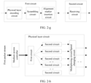
- FIG. 2-g A possible circuit structure in this application scenario may be shown in FIG. 2-g .
- a first circuit includes a physical layer encoding circuit, a scrambling circuit, an alignment marker insertion circuit.
- a first circuit processes a received first data block stream to obtain a first data stream; the first circuit distributes the first data stream to N1 second circuits of M second circuits in a physical layer circuit, where M is greater than N1, and N1 and M are positive integers; and the N1 second circuits process the received first data stream to obtain N1 first code streams.
- the first circuit may selectively distribute the first data stream to the N1 second circuits of the M second circuits in the physical layer circuit as required, and does not need to distribute the first data stream to all the M second circuits in the physical layer circuit, this helps to implement that a physical layer sub-circuit with a corresponding processing capability is configured based on a size of an upper-layer packet stream, and diversified bandwidth modes instead of a fixed single bandwidth mode are presented externally.
- the technical solutions of the embodiments help to enhance flexibility of Ethernet bandwidth configuration and increase a resource reuse rate to a certain extent, to further meet a requirement for complex bandwidth configuration and extend an application scenario.
- At least one second circuit except the N1 second circuits may be further disabled. By disabling some idle second circuits, energy consumption may be reduced.
- a maximum processing rate that can be provided by the N1 second circuits is greater than or equal to a rate of the first data block stream.
- the number of participating second circuits may be determined (that is, a value of N1 is determined) based on the rate of the first data block stream.
- N1 second circuits may also be directly configured to participate in related processing on the first data block stream. If the maximum processing rate that can be provided by the N1 second circuits is greater than or equal to the rate of the first data block stream, it is ensured that the first data block stream is processed instantly.
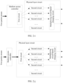
- the data distribution method may further include: sending, by the N1 second circuits, the N1 first code streams to a multiplexing circuit (multiplexer); performing, by the multiplexing circuit, multiplexing processing on the N1 first code streams to obtain X second code streams, where X is a positive integer less than or equal to N1, for example, X is equal to 1, 2, 3, or another positive integer.
- a possible circuit structure may be shown in FIG. 2-h and FIG. 2-i , where the multiplexing circuit performs multiplexing processing on the N1 first code streams to obtain X second code streams.
- FIG. 2-h and FIG. 2-i also show that the multiplexing circuit may be replaced with a gearbox (gearbox) to change a rate of the first code streams.
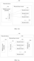
- the data distribution method may further include: sending, by N12 second circuits of the N1 second circuits, N12 first code streams to the multiplexing circuit; performing, by the multiplexing circuit, multiplexing processing on the N12 first code streams to obtain X2 second code streams, where X2 is a positive integer less than or equal to N12, for example, X2 may be equal to 1, 2, 3, or another positive integer.
- X2 is a positive integer less than or equal to N12, for example, X2 may be equal to 1, 2, 3, or another positive integer.
- FIG. 2-j and FIG. 2-k show that the multiplexing circuit may be replaced with a gearbox to change a rate of the first code streams.
- the following describes an example of some application scenarios in which interaction is performed with a peer device (that is, a receiving apparatus).
- the receiving apparatus may be a router, a network switch, a firewall, a data center, a wavelength division multiplexing device, a load balancer, or another type of network device.
- the data distribution method may further include: sending, by the N1 second circuits, the N1 first code streams to a PHY of the receiving apparatus, where the number of third circuits in the PHY of the receiving apparatus is N1 and the N1 first code streams are in a one-to-one correspondence with the N1 third circuits.
- Each third circuit includes an alignment marker removal circuit, a descrambling circuit, and a physical layer decoding circuit; or, each third circuit includes an alignment marker removal circuit and a descrambling circuit; or, each third circuit includes an alignment marker removal circuit; or, each third circuit includes a receiving circuit.
- a possible circuit structure may be shown in FIG. 2-l .
- the N1 second circuits may send the N1 first code streams to the PHY of the receiving apparatus, where the number of third circuits in the PHY of the receiving apparatus is N1.
- the data distribution method may further include: sending, by the N1 second circuits, the N1 first code streams to a PHY of a receiving apparatus, where the PHY of the receiving apparatus may include M2 third circuits, and the N1 first code streams are in a one-to-one correspondence with N1 third circuits of the M2 third circuits.
- Each third circuit includes an alignment marker removal circuit, a descrambling circuit, and a physical layer decoding circuit; or, each third circuit includes an alignment marker removal circuit and a descrambling circuit; or, each third circuit includes an alignment marker removal circuit; or, each third circuit includes a receiving circuit.
- M2 is greater than, equal to, or less than M.
- a possible circuit structure may be shown in FIG. 2-m . As shown in FIG. 2-m , the N1 second circuits send the N1 first code streams to the PHY of the receiving apparatus, where the number of third circuits in the PHY of the receiving apparatus is M2.
- the first circuit and N2 second circuits of the M second circuits may further process another packet stream (which may be called a second packet stream), which helps to further increase a circuit reuse rate.
- the data distribution method may further include:
- first and “second” in the first packet stream and the second packet stream are used to differentiate packet streams of different attributes.
- An attribute of “the first packet stream” is different from an attribute of "the second packet stream”.
- a header of a packet in “the first packet stream” is different from a header of a packet in "the second packet stream”.
- a header of a packet may be an outer header of the packet or a header carried in the packet.
- an outer header of an IP packet is an IP header.
- a layer of the header carried in the IP packet may be layer 2.5, layer 3, or layer 4.
- a layer 2.5 protocol may be the Multiprotocol Label Switching (multiprotocol label switching, MPLS for short) protocol.
- a layer 3 protocol may be IP.
- a layer 4 protocol may be the Transmission Control Protocol (transmission control protocol, TCP for short).
- An outer header of an Ethernet frame is a frame header.
- a layer of the header carried in the Ethernet frame may be layer 2.5, layer 3, or layer 4.
- For layer 2.5, layer 3, or layer 4 refer to the Open System Interconnection--Reference Model (open system interconnection reference model).
- the receiving apparatus may be a router, a network switch, a firewall, a data center, a wavelength division multiplexing device, a load balancer, or another type of network device.
- the data distribution method may further include: sending, by the N1 second circuits, the N1 first code streams to a PHY of a first receiving apparatus, where the PHY of the first receiving apparatus includes N1 third circuits, and the N1 first code streams are in a one-to-one correspondence with the N1 third circuits; and each third circuit includes an alignment marker removal circuit, a descrambling circuit, and a physical layer decoding circuit; or, each third circuit includes an alignment marker removal circuit and a descrambling circuit; or, each third circuit includes an alignment marker removal circuit; or, each third circuit includes a receiving circuit.
- the N2 second circuits further send the N2 third code streams to a PHY of a second receiving apparatus, where the PHY of the second receiving apparatus includes N2 fourth circuits, the N2 third code streams are in a one-to-one correspondence with the N2 fourth circuits, and the first receiving apparatus is different from the second receiving apparatus.
- Each fourth circuit includes an alignment marker removal circuit, a descrambling circuit, and a physical layer decoding circuit; or, each fourth circuit includes an alignment marker removal circuit and a descrambling circuit; or, each fourth circuit includes an alignment marker removal circuit; or, each fourth circuit includes a receiving circuit.
- a possible circuit structure may be shown in FIG.
- N1 second circuits send the N1 first code streams to the PHY of the first receiving apparatus
- the N2 second circuits send the N2 first code streams to the PHY of the second receiving apparatus.
- the number of third circuits in the PHY of the first receiving apparatus is N1.
- the number of fourth circuits in the PHY of the second receiving apparatus is N2.
- the data distribution method may further include: sending, by the N1 second circuits, the N1 first code streams to a first PHY of a receiving apparatus, where the first PHY includes N1 third circuits, and the N1 first code streams are in a one-to-one correspondence with the N1 third circuits.
- Each third circuit includes an alignment marker removal circuit, a descrambling circuit, and a physical layer decoding circuit; or, each third circuit includes an alignment marker removal circuit and a descrambling circuit; or, each third circuit includes an alignment marker removal circuit; or, each third circuit includes a receiving circuit.
- the N2 second circuits may further send the N2 third code streams to a second PHY of the receiving apparatus, where the second PHY of the receiving apparatus includes N2 fourth circuits, and the N2 third code streams are in a one-to-one correspondence with the N2 fourth circuits.
- Each fourth circuit includes an alignment marker removal circuit, a descrambling circuit, and a physical layer decoding circuit; or, each fourth circuit includes an alignment marker removal circuit and a descrambling circuit; or, each fourth circuit includes an alignment marker removal circuit; or, each fourth circuit includes a receiving circuit.
- a possible circuit structure may be shown in FIG.
- N1 second circuits send the N1 first code streams to the first PHY of the receiving apparatus
- the N2 second circuits send the N2 first code streams to the second PHY of the receiving apparatus.
- the number of third circuits in the first PHY of the receiving apparatus is N1.
- the number of fourth circuits in the second PHY of the receiving apparatus is N2.
- a local network device may also perform data transmission with another device in another manner, which is not further described herein.
- a network layer of a network device produces a first packet stream with a maximum rate of 100 Gpbs and a second packet stream with a maximum rate of 200 Gpbs simultaneously, where a maximum processing capability of a MAC and a PHY of the network device is 400Gpbs; and it is assumed that the PHY has 16 second circuits, where a maximum processing rate of each second circuit is 25 Gpbs. Therefore, 4 second circuits of the 16 second circuits are configured to perform related processing on the first packet stream, and 8 second circuits of the 16 second circuits are configured to perform related processing on the first packet stream.
- the first circuit includes a physical layer encoding circuit, and each second circuit includes a scrambling circuit and an alignment marker insertion circuit.
- the MAC After receiving the first packet stream, the MAC divides the first packet stream to obtain a first data block stream; the MAC sends the first data block stream to the first circuit; the physical layer encoding circuit in the first circuit performs physical layer encoding processing on the first data block stream to obtain a first data stream; the first circuit distributes the first data stream (that is, the first data stream is divided into 4 parts) to the 4 second circuits of the 16 second circuits in the PHY; and the 4 second circuits perform scrambling circuit and alignment marker insertion processing on the received first data stream to obtain 4 first code streams, where the 4 second circuits are in a one-to-one correspondence with the 4 first code streams.
- the MAC divides the second packet stream into a second data block stream; the MAC sends the second data block stream to the first circuit; the physical layer encoding circuit in the first circuit performs physical layer encoding processing on the second data block stream to obtain a second data stream; the first circuit distributes the second data stream (that is, the second data stream is divided into 8 parts) to 8 second circuits (certainly, the 8 second circuits are different from the foregoing 4 second circuits) of the 16 second circuits in the PHY; and the 8 second circuits perform scrambling circuit and alignment marker insertion processing on the received second data stream to obtain 8 third code streams, where the 8 second circuits are in a one-to-one correspondence with the 8 third code streams.
- the PHY may disable the 4 idle second circuits.
- the network device can simultaneously process a plurality of packet streams corresponding to different services, support interface configuration of a smaller granularity, and can present interfaces of a plurality of rates externally, which helps to implement more flexible networking, improve resource utilization, and reduce energy consumption, and further helps to meet a requirement for complex bandwidth configuration and extend an application scenario.
- interface configuration of a smaller granularity may be supported, and the number of second circuits participating in processing may be dynamically configured as required, which helps to implement more flexible networking.
- the MAC and the PHY may have different working bandwidth (for example, the bandwidth of the MAC is 400 G, while the PHY may include 40 second circuits with a 10 G bandwidth each).
- the number of working second circuits in the PHY may be configured, which helps to implement a seamless IP+optical combination with a future optical network of flexible bandwidth, and resolve a problem of possible load imbalance between different links in a case of per-flow/per-packet load sharing.
- a mechanism such as a hierarchical distribution and aggregation mechanism, and a pre-processing mechanism may be used to achieve a purpose of further saving resources.
- the following further provides a related apparatus configured to implement the data distribution solution.
- an embodiment of the present invention further provides a network device 300.
- the network device 300 may be configured to perform the method shown in FIG. 2-a .
- the network device 300 may be a router, a network switch, a firewall, a data center, a wavelength division multiplexing device, a load balancer, or another type of network device.
- the network device 300 may include: a MAC 310 and a PHY 320.
- the MAC 310 is configured to receive a first packet stream, divide the first packet stream to obtain a first data block stream, and send the first data block stream to a first circuit.
- the first circuit 311 is configured to process the first data block stream to obtain a first data stream, and distribute the first data stream to N1 second circuits of M second circuits in the PHY; where M is greater than N1, N1 is a positive integer, and M is a positive integer.
- that the MAC 310 divides the first packet stream to obtain a first data block stream, and sends the first data block stream to a first circuit may include that: a blocking circuit in the MAC 310 divides the first packet stream into the first data block stream, and sending the first data block stream to the first circuit 311.
- N1 second circuits 321 are configured to process the received first data stream to obtain N1 first code streams, where the N1 second circuits are in a one-to-one correspondence with the N1 first code streams.
- the first circuit 311 includes a receiving circuit, and the first data stream is the first data block stream.
- Each second circuit 321 of the M second circuits 321 includes a physical layer encoding circuit, a scrambling circuit, and an alignment marker insertion circuit.
- the first circuit 311 includes a physical layer encoding circuit; the first data stream is a data stream that is obtained after physical layer encoding is performed on the first data block stream, each second circuit 321 of the M second circuits 321 includes a scrambling circuit and an alignment marker insertion circuit, and the first circuit 311 is a circuit in the PHY 320.
- the first circuit 311 includes a physical layer encoding circuit and a scrambling circuit; the first data stream is a data stream that is obtained after physical layer encoding and scrambling are performed on the first data block stream, each second circuit 321 of the M second circuits 321 includes an alignment marker insertion circuit, and the first circuit 311 is a circuit in the PHY 320.
- the first circuit 311 may include a physical layer encoding circuit, a scrambling circuit, and an alignment marker insertion circuit; the first data stream is a data stream that is obtained after physical layer encoding, scrambling, and alignment marker insertion are performed on the first data block stream, each second circuit 321 of the M second circuits 321 includes a receiving circuit, and the first circuit 311 is a circuit in the PHY 320.
- the first packet stream refers to a data stream including a plurality of packets.
- the first packet stream may be an IP packet stream or an Ethernet frame stream.
- the IP packet stream refers to a data stream including a plurality of IP packets.
- the Ethernet frame stream refers to a data stream including a plurality of Ethernet frames.
- the PHY 320 is further configured to disable, in the M second circuits 321, at least one second circuit 320 except the N1 second circuits 321.
- a maximum processing rate that can be provided by the N1 second circuits 321 is greater than or equal to a rate of the first data block stream.
- the network device 300 may further include: a multiplexing circuit 330; and the N1 second circuits 321 are further configured to send N1 first code streams to the multiplexing circuit 330.
- the multiplexing circuit 330 is configured to perform multiplexing processing on the N1 first code streams to obtain X second code streams, where X is a positive integer less than or equal to N1.
- the MAC 310 may be further configured to receive a second packet stream, divide the second packet stream into a second data block stream, and send the second data block stream to the first circuit;
- the second data stream is the second data block stream.
- the second data stream is a data stream that is obtained after physical layer encoding is performed on the second data block stream.
- the second data stream is a data stream that is obtained after physical layer encoding and scrambling are performed on the second data block stream.
- the second data stream is a data stream that is obtained after physical layer encoding, scrambling, and alignment marker insertion are performed on the second data block stream.
- first and “second” in the first packet stream and the second packet stream are used to differentiate packet streams of different attributes.
- An attribute of “the first packet stream” is different from an attribute of "the second packet stream”.
- a header of a packet in “the first packet stream” is different from a header of a packet in "the second packet stream”.
- a header of a packet may be an outer header of the packet or a header carried in the packet.
- an outer header of an IP packet is an IP header.
- a layer of the header carried in the IP packet may be layer 2.5, layer 3, or layer 4.
- a layer 2.5 protocol may be the MPLS protocol.
- a layer 3 protocol may be IP.
- a layer 4 protocol may be TCP.
- An outer header of an Ethernet frame may be a frame header.
- a layer of the header carried in the Ethernet frame may be layer 2.5, layer 3, or layer 4.
- layer 2.5, layer 3 or layer 4 refer to the Open System Interconnection--Reference Model.
- the N1 second circuits 321 are further configured to send the N1 first code streams to a PHY of a receiving apparatus.
- the PHY of the receiving apparatus may, for example, include only N1 third circuits, and the N1 first code streams are in a one-to-one correspondence with the N1 third circuits.
- Each third circuit includes an alignment marker removal circuit, a descrambling circuit, and a physical layer decoding circuit; or, each third circuit includes an alignment marker removal circuit and a descrambling circuit; or, each third circuit includes an alignment marker removal circuit; or, each third circuit includes a receiving circuit.
- the N1 second circuits 321 are further configured to send the N1 first code streams to a PHY of a receiving apparatus, where the PHY of the receiving apparatus may include M2 third circuits, and the N1 first code streams are in a one-to-one correspondence with the N1 third circuits of the M2 third circuits.
- Each third circuit includes an alignment marker removal circuit, a descrambling circuit, and a physical layer decoding circuit; or, each third circuit includes an alignment marker removal circuit and a descrambling circuit; or, each third circuit includes an alignment marker removal circuit; or, each third circuit includes a receiving circuit.
- M2 is greater than, equal to, or less than M.
- the N1 second circuits 321 may be further configured to send the N1 first code streams to a PHY of a first receiving apparatus, where the PHY of the first receiving apparatus includes N1 third circuits, and the N1 first code streams are in a one-to-one correspondence with the N1 third circuits; and each third circuit includes an alignment marker removal circuit, a descrambling circuit, and a physical layer decoding circuit; or, each third circuit includes an alignment marker removal circuit and a descrambling circuit; or, each third circuit includes an alignment marker removal circuit; or, each third circuit includes a receiving circuit.
- the N2 second circuits 321 may be further configured to send N2 second code streams to a PHY of a second receiving apparatus, where the PHY of the second receiving apparatus includes N2 fourth circuits, and the N2 second code streams are in a one-to-one correspondence with the N2 fourth circuits.
- the first receiving apparatus is different from the second receiving apparatus, and each fourth circuit includes an alignment marker removal circuit, a descrambling circuit, and a physical layer decoding circuit; or, each fourth circuit includes an alignment marker removal circuit and a descrambling circuit; or, each fourth circuit includes an alignment marker removal circuit; or, each fourth circuit includes a receiving circuit.
- the N1 second circuits 321 may be further configured to send the N1 first code streams to a first PHY of a receiving apparatus.
- the first PHY includes N1 third circuits, and the N1 first code streams are in a one-to-one correspondence with the N1 third circuits.
- Each third circuit includes an alignment marker removal circuit, a descrambling circuit, and a physical layer decoding circuit; or, each third circuit includes an alignment marker removal circuit and a descrambling circuit; or, each third circuit includes an alignment marker removal circuit; or, each third circuit includes a receiving circuit.
- the N2 second circuits 321 may be further configured to send the N2 second code streams to a second PHY of a receiving apparatus, where the second PHY of the receiving apparatus includes N2 fourth circuits, and the N2 second code streams are in a one-to-one correspondence with the N2 fourth circuits.
- Each fourth circuit includes an alignment marker removal circuit, a descrambling circuit, and a physical layer decoding circuit; or, each fourth circuit includes an alignment marker removal circuit and a descrambling circuit; or, each fourth circuit includes an alignment marker removal circuit; or, each fourth circuit includes a receiving circuit.
- a first circuit of a network device 300 processes a received first data block stream to obtain a first data stream; the first circuit distributes the first data stream to N1 second circuits of M second circuits in a physical layer circuit, where M is greater than N1, and the N1 and the M are positive integers; and the N1 second circuits process the received first data stream to obtain N1 first code streams.
- the first circuit may selectively distribute the first data stream to the N1 second circuits of the M second circuits in the physical layer circuit as required, and does not need to distribute the first data stream to all the M second circuits in the physical layer circuit, this helps to implement that a physical layer sub-circuit with a corresponding processing capability is configured based on a size of an upper-layer packet stream, and diversified bandwidth modes instead of a fixed single bandwidth mode are presented externally.
- the technical solutions of the embodiments help to enhance flexibility of Ethernet bandwidth configuration and increase a resource reuse rate to a certain extent, to further meet a requirement for complex bandwidth configuration and extend an application scenario.
- interface configuration of a smaller granularity may be supported, and the number of second circuits participating in processing may be dynamically configured as required, which helps to implement more flexible networking.
- the MAC and the PHY may have different working bandwidth (for example, the bandwidth of the MAC is 400 G, while the PHY may include 40 second circuits with a 10 G bandwidth each).
- the number of working second circuits in the PHY may be configured, which helps to implement a seamless IP+optical combination with a future optical network of flexible bandwidth, and resolve a problem of possible load imbalance between different links in a case of per-flow/per-packet load sharing.
- a mechanism such as a hierarchical distribution and aggregation mechanism, and a pre-processing mechanism may be used to achieve a purpose of further saving resources.
- a data aggregation method may specifically include: receiving, by N3 first circuits of M first circuits in a PHY, N3 first code streams, where the N3 first circuits are in a one-to-one correspondence with the N3 first code streams; processing, by the N3 first circuits, the received N3 first code streams to obtain N3 first data streams; sending, by the N3 first circuits, the N3 first data streams to a second circuit; processing, by the second circuit, the N3 first data streams to obtain a first data block stream; and combining the first data block stream to obtain a first packet stream.
- the second circuit includes a receiving circuit, the first data block stream is a data block stream obtained by aggregating the N3 first data streams, the N3 first data streams are data streams that are obtained after alignment marker removal, descrambling, and physical layer decoding are performed on the N3 first code streams, and each first circuit of the M first circuits includes an alignment marker removal circuit, a descrambling circuit, and a physical layer decoding circuit; or, the second circuit includes a physical layer decoding circuit, the first data block stream is a data block stream that is obtained after physical layer decoding is performed on the N3 first data streams, the N3 first data streams are data streams that are obtained after alignment marker removal and descrambling are performed on the N3 first code streams, each first circuit of the M first circuits includes an alignment marker removal circuit and a descrambling circuit, and the second circuit is a circuit in the PHY; or, the second circuit includes a descrambling circuit and a physical layer decoding circuit, the first data block stream is a data block stream that is obtained after descram
- FIG. 4-a is a schematic flowchart of a data aggregation method according to an embodiment of the present invention.
- An entity for executing the data aggregation method may be a network device.
- the network device may be a router, a network switch, a firewall, a data center, a wavelength division multiplexing device, a load balancer, or another type of network device.
- the data aggregation method according to the embodiment of the present invention may include the following content: 401. N3 first circuits of M first circuits in a PHY receive N3 first code streams.
- the N3 first circuits are in a one-to-one correspondence with the N3 first code streams.
- the N3 first code streams may be obtained in the following way: dividing a packet stream into a data block stream; distributing the data block stream to obtain N3 sub data block streams; performing physical layer encoding on the N3 sub data block streams to obtain N3 sub data block streams that have undergone the physical layer encoding; performing scrambling on the N3 sub data block streams that have undergone the physical layer encoding to obtain N3 scrambled sub data block streams; and performing alignment marker insertion on the N3 scrambled sub data block streams to obtain N3 first code streams.
- the N3 first code streams may be obtained in the following way: dividing a packet stream into a data block stream; performing physical layer encoding on the data block stream to obtain a data block stream that has undergone the physical layer encoding; distributing the data block stream that has undergone the physical layer encoding to obtain N3 sub data block streams that have undergone the physical layer encoding; performing scrambling on the N3 sub data block streams that have undergone the physical layer encoding to obtain N3 scrambled sub data block streams; and performing alignment marker insertion on the N3 scrambled sub data block streams to obtain N3 first code streams.
- the N3 first code streams may be obtained in the following way: dividing a packet stream into a data block stream; performing physical layer encoding on the data block stream to obtain a data block stream that has undergone the physical layer encoding; performing scrambling on the data block stream that has undergone the physical layer encoding to obtain a scrambled data block stream; dividing the scrambled data block stream into N3 scrambled sub data block streams; and performing alignment marker insertion on the N3 scrambled sub data block streams to obtain N3 first code streams.
- the N3 first code streams may be obtained in the following way: dividing a packet stream into a data block stream; performing physical layer encoding on the data block stream to obtain a data block stream that has undergone the physical layer encoding; performing scrambling on the data block stream that has undergone the physical layer encoding to obtain a scrambled data block stream; performing alignment marker insertion on the scrambled data block stream to obtain a code stream; and distributing the code stream to obtain N3 first code streams.
- a first code stream of the N3 first code streams may be a serial bit stream.
- the N3 first code streams may be bit streams sent by a serdes.
- the N3 first circuits process the received N3 first code streams to obtain N3 first data streams.
- the N3 first circuits send the N3 first data streams to a second circuit.
- the second circuit processes the N3 first data streams to obtain a first data block stream.
- An entity for executing step 405 may be a MAC.
- the first data block stream includes a plurality of data blocks.
- the combining the first data block stream to obtain a first packet stream may specifically include: combining a plurality of data blocks that are in the first data block stream and belong to a same packet into a packet, where a plurality of combined packets forms a first packet stream.
- the second circuit may send the first data block stream to a block combining circuit in the MAC, and the block combining circuit in the MAC combines the first data block stream to obtain a first packet stream.
- FIG. 4-b and FIG. 4-c are two types of network devices capable of implementing the data aggregation method shown in FIG. 4-a according to the embodiment of the present invention.
- the network devices shown in FIG. 4-b and FIG. 4-c include a MAC and a PHY each.
- the MAC includes a second circuit
- the PHY includes M first circuits.
- the PHY includes a second circuit and M first circuits.
- the second circuit includes a receiving circuit, and the first data block stream is a data block stream obtained by aggregating the N3 first data streams.
- the N3 first data streams are data streams that are obtained after alignment marker removal, descrambling, and physical layer decoding are performed on the N3 first code streams.
- Each first circuit of the M first circuits includes an alignment marker removal circuit, a descrambling circuit, and a physical layer decoding circuit.
- that the second circuit processes the N3 first data streams to obtain a first data block stream may include that: the second circuit performs aggregation processing on the N3 first data streams to obtain the first data block stream.
- That the N3 first circuits process the received N3 first code streams to obtain N3 first data streams may specifically include that: the N3 first circuits perform alignment marker removal processing on the received N3 first code streams (the alignment marker removal circuit in each first circuit may perform alignment marker removal processing on the received first data stream), performing descrambling processing on the code streams that have undergone the alignment marker removal processing (the descrambling circuit in each first circuit may perform descrambling processing on the code streams that have undergone the alignment marker removal processing), and performing physical layer decoding processing on the code streams that have undergone the descrambling processing (the physical layer decoding circuit in each first circuit may perform physical layer decoding processing on the code streams that have undergone the descrambling circuit), to obtain the N3 first data streams.
- the N3 first circuits perform alignment marker removal processing on the received N3 first code streams (the alignment marker removal circuit in each first circuit may perform alignment marker removal processing on the received first data stream), performing descrambling processing on the code streams that have undergone the alignment marker removal processing on the code streams that have undergone
- FIG. 4-d a possible circuit structure may be shown in FIG. 4-d .
- a second circuit includes a receiving circuit
- a first circuit includes a physical layer decoding circuit, a descrambling circuit, and an alignment marker removal circuit.
- the physical layer decoding may be 5b/4b decoding, 10b/8b decoding, 66b/64b decoding, or another type of physical layer decoding.
- the second circuit may include a physical layer decoding circuit, where the first data block stream is a data block stream that is obtained after physical layer decoding is performed on the N3 first data streams.
- the N3 first data streams are data streams that are obtained after alignment marker removal and descrambling are performed on the N3 first code streams.
- Each first circuit of the M first circuits includes an alignment marker removal circuit and a descrambling circuit, and the second circuit is a circuit in a PHY.
- that the second circuit processes the N3 first data streams to obtain a first data block stream may include that: the second circuit performs physical layer decoding processing on the N3 first data streams to obtain the first data block stream.
- That the N3 first circuits process the received N3 first code streams to obtain N3 first data streams may specifically include that: the N3 first circuits perform alignment marker removal processing on the received N3 first code streams (the alignment marker removal circuit in each first circuit may perform alignment marker removal processing on the received first data stream), and performing descrambling processing on the code streams that have undergone the alignment marker removal processing (the descrambling circuit in each first circuit may perform descrambling processing on the code streams that have undergone the alignment marker removal processing), to obtain the N3 first data streams.
- a possible circuit structure may be shown in FIG. 4-e .
- a second circuit includes a physical layer decoding circuit
- a first circuit includes a descrambling circuit and an alignment marker removal circuit.
- the second circuit may include a descrambling circuit and a physical layer decoding circuit, where the first data block stream is a data block stream that is obtained after descrambling and physical layer decoding are performed on the N3 first data streams.
- the N3 first data streams are data streams that are obtained after alignment marker removal is performed on the N3 first code streams.
- Each first circuit of the M first circuits includes an alignment marker removal circuit.
- the second circuit is a circuit in a PHY.
- that the second circuit processes the N3 first data streams to obtain a first data block stream may include that: the second circuit performs descrambling processing on the N3 first data streams (the descrambling circuit in the second circuit may perform descrambling processing on the N3 first data streams), and performing physical layer decoding processing on the data streams that have undergone the descrambling processing (the physical layer decoding circuit in the second circuit may perform physical layer decoding processing on the data streams that have undergone the descrambling processing), to obtain the first data block stream.
- That the N3 first circuits process the received N3 first code streams to obtain N3 first data streams may include that: the N3 first circuits perform alignment marker removal processing on the received N3 first code streams (the alignment marker removal circuit in each first circuit may perform alignment marker removal processing on the received first code streams) to obtain the N3 first data streams.
- a possible circuit structure may be shown in FIG. 4-f .
- a second circuit includes a physical layer decoding circuit and a descrambling circuit
- a first circuit includes an alignment marker removal circuit.
- the second circuit may also include an alignment marker removal circuit, a descrambling circuit, and a physical layer decoding circuit.
- the first data block stream is a data block stream that is obtained after alignment marker removal, descrambling, and physical layer decoding are performed.
- the N3 first data streams are N3 first code streams, and the second circuit is a circuit in a PHY
- Each first circuit of the M first circuits includes a receiving circuit.
- that the second circuit processes the N3 first data streams to obtain a first data block stream may include that: the second circuit performs alignment marker removal processing on the N3 first data streams (specifically, the alignment marker removal circuit in the second circuit may perform alignment marker removal processing on the N3 first data streams), performing descrambling processing on the data streams that have undergone the alignment marker removal processing (specifically, the descrambling circuit in the second circuit may perform descrambling processing on the N3 first data streams), and performing physical layer decoding processing on the data streams that have undergone the descrambling processing (the physical layer decoding circuit in the second circuit may perform physical layer decoding processing on the data streams that have undergone the descrambling processing), to obtain the first data block stream.
- the second circuit performs alignment marker removal processing on the N3 first data streams
- the alignment marker removal circuit in the second circuit may perform alignment marker removal processing on the N3 first data streams
- performing descrambling processing on the data streams that have undergone the alignment marker removal processing specifically, the descrambling circuit in the second circuit may perform des
- That the N3 first circuits process the received N3 first code streams to obtain N3 first data streams may include that: the N3 first circuits perform receiving processing on the received N3 first code streams to obtain the N3 first data streams.
- a possible circuit structure in this application scenario may be shown in FIG. 4-g .
- a second circuit includes a physical layer decoding circuit, a descrambling circuit, an alignment marker removal circuit.
- At least one first circuit except the N3 first circuits may be further disabled. By disabling some idle second circuits, energy consumption may be reduced.
- a maximum processing rate that can be provided by the N3 first circuits is greater than or equal to a rate of the N3 first code streams.
- the number of participating first circuits may be determined (that is, a value of N3 is determined) based on the rate of the first data block stream.
- N3 first circuits may also be directly configured to participate in related processing on the first code streams. If the maximum processing rate that can be provided by the N2 first circuits is greater than or equal to the rate of the first code streams, it is ensured that the first code streams are processed instantly.
- the data aggregation method may further include: receiving, by a demultiplexing circuit (demultiplexer), X second code streams; performing, by the demultiplexing circuit, demultiplexing processing on the X second code streams to obtain N3 first code streams, and sending the N3 first code streams to the N3 first circuits; where X is a positive integer less than or equal to N3, for example, X is equal to 1, 2, 3, or another positive integer.
- a possible circuit structure may be shown in FIG. 4-h , where the demultiplexing circuit performs multiplexing processing on the X second code streams to obtain N3 first code streams.
- the data aggregation method may further include: receiving, by N4 first circuits of the M first circuits, N4 third code streams, and processing, by the N4 first circuits, the received N4 third code streams to obtain N4 second data streams; sending, by the N4 first circuits, the N4 second data streams to a second circuit; processing, by the second circuit, the N4 second data streams to obtain a second data block stream; and combining the second data block stream into a second packet stream.
- the N4 first circuits are in a one-to-one correspondence with the N4 third code streams.
- An intersection between the N4 first circuits and the N3 first circuits is an empty set (that is, any first circuit of the N4 first circuits is different from any first circuit of the N2 first circuits. It may be understood that N4 + N3 is less than or equal to M).
- the second data block stream is a data block stream obtained by aggregating the N4 second data streams, and the N4 second data streams are data streams that are obtained after alignment marker removal, descrambling, and physical layer decoding are performed on the N4 third code streams; or, the second data block stream is a data block stream that is obtained after physical layer decoding is performed on the N4 second data streams, and the N4 second data streams are data streams that are obtained after alignment marker removal and descrambling are performed on the N4 third code streams; or, the second data block stream is a data block stream that is obtained after descrambling and physical layer decoding are performed on the N4 second data streams, and the N4 second data streams are data streams that are obtained after alignment marker removal is performed on the N4 third code streams; or, the second data block stream is a data block stream that is obtained after alignment marker removal, descrambling, and physical layer decoding are performed, and the N4 second data streams are the N4 third code streams.
- a network device receives 4 first code streams with a maximum rate of 100 Gpbs (the maximum rate of each code stream is 25 Gpbs) from a first router and receives 8 third code streams with a maximum rate of 200 Gpbs (the maximum rate of each code stream is 25 Gpbs), where a maximum processing capability of a MAC and a PHY of the network device is 400 Gpbs; and it is assumed that the PHY has 16 first circuits, where a maximum processing rate of each first circuit is 25 Gpbs. Therefore, 4 first circuits of the 16 first circuits are configured to perform related processing on the 4 first code streams, and 8 first circuits of the 16 first circuits are configured to perform related processing on the third code streams.
- the second circuit includes a receiving circuit, and each first circuit includes an alignment marker removal circuit, a descrambling circuit, and a physical layer decoding circuit.
- the 4 first circuits After receiving the 4 first code streams, the 4 first circuits perform alignment marker removal processing, descrambling processing, and physical layer decoding processing on the 4 first code streams to obtain 4 first data streams; the 4 first circuits send the 4 first data streams to the second circuit; the first circuit performs aggregation processing on the 4 first data streams to obtain a first data block stream (that is, the 4 first data streams are aggregated into a first data block stream), and sends the first data block stream to the MAC; and the MAC combines the first data block stream to obtain a first packet stream.
- the 4 first circuits are in a one-to-one correspondence with the 4 first code streams.
- the 8 first circuits (certainly, the 8 first circuits are different from the foregoing 4 first circuits) perform alignment marker removal processing, descrambling processing, and physical layer decoding processing on the 8 third code streams to obtain 8 second data streams, and the 8 first circuits send the 8 second data streams to the second circuit; the second circuit performs aggregation processing on the 8 second data streams to obtain a second data block stream (that is, the 8 second data streams are aggregated into one second data block stream), and sends the second data block stream to the MAC; and the MAC combines the second data block stream into a second packet stream.
- the 8 first circuits are in a one-to-one correspondence with the 8 third code streams.
- the PHY may disable the 4 idle first circuits.
- the network device can simultaneously process a plurality of packet streams corresponding to different services, support interface configuration of a smaller granularity, and can present interfaces of a plurality of rates externally, which helps to implement more flexible networking, improve resource utilization, and reduce energy consumption.
- N3 first circuits of M first circuits in a PHY receive N3 first code streams, where the N3 first circuits are in a one-to-one correspondence with the N3 first code streams; the N3 first circuits process the received N3 first code streams to obtain N3 first data streams; the N3 first circuits send the N3 first data streams to a second circuit; the second circuit processes the N3 first data streams to obtain a first data block stream.
- the PHY may selectively use the N3 first circuits of the M first circuits to receive the N3 first code streams as required, and does not need to use all the M first circuits in the PHY to receive code streams, this helps to implement that a physical layer sub-circuit with a corresponding processing capability is configured based on a size of a transmitted code stream, and diversified bandwidth modes instead of a fixed single bandwidth mode are presented externally.
- the technical solutions of the embodiments help to enhance flexibility of Ethernet bandwidth configuration and increase a resource reuse rate to a certain extent, to further meet a requirement for complex bandwidth configuration and extend an application scenario.
- interface configuration of a smaller granularity may be supported, and the number of first circuits participating in processing may be dynamically configured as required, which helps to implement more flexible networking.
- the MAC and the PHY may have different working bandwidth (for example, the bandwidth of the MAC is 400 G, while the PHY may include 40 first circuits with a 10 G bandwidth each).
- the number of working first circuits in the PHY may be configured, which helps to implement a seamless IP+optical combination with a future optical network of flexible bandwidth, and resolve a problem of possible load imbalance between different links in a case of per-flow/per-packet load sharing.
- a mechanism such as a hierarchical distribution and aggregation mechanism, and a pre-processing mechanism may be used to achieve a purpose of further saving resources.
- an embodiment of the present invention further provides a network device 500.
- the network device 500 may be configured to perform the method shown in FIG. 4-a .
- the network device 500 may be a router, a network switch, a firewall, a data center, a wavelength division multiplexing device, a load balancer, or another type of network device.
- the network device 500 may include: a PHY 510 and a MAC 520.
- N3 first circuits 511 of M first circuits 511 in the PHY 510 are configured to receive N3 first code streams, and process the received first code streams to obtain N3 first data streams, and send the N3 first data streams to a second circuit 521.
- the N3 first circuits 511 are in a one-to-one correspondence with the N3 first code streams.
- that the second circuit 521 sends a first data block stream to the MAC 520 may specifically include that: the second circuit 521 sends the first data block stream to a block combining circuit in the MAC 520. Specifically, the block combining circuit in the MAC 520 combines the first data block stream to obtain a first packet stream.
- the second circuit 521 is configured to process the N3 first data streams to obtain the first data block stream.
- the MAC 520 is configured to combine the first data block stream into the first packet stream.
- the second circuit 521 includes a receiving circuit
- the first data block stream is a data block stream obtained by aggregating the N3 first data streams
- the N3 first data streams are data streams that are obtained after alignment marker removal, descrambling, and physical layer decoding are performed on the N3 first code streams
- each first circuit 511 of the M first circuits 511 includes an alignment marker removal circuit, a descrambling circuit, and a physical layer decoding circuit.
- the second circuit 521 includes a physical layer decoding circuit; the first data block stream is a data block stream that is obtained after physical layer decoding is performed on the N3 first data streams, the N3 first data streams are data streams that are obtained after alignment marker removal and descrambling are performed on the N3 first code streams, each first circuit 511 of the M first circuits 511 includes an alignment marker removal circuit and a descrambling circuit, and the second circuit 521 is a circuit in the PHY 510.
- the second circuit 521 includes a descrambling circuit and a physical layer decoding circuit;
- the first data block stream is a data block stream that is obtained after descrambling and physical layer decoding are performed on the N3 first data streams,
- the N3 first data streams are data streams that are obtained after alignment marker removal is performed on the N3 first code streams,
- each first circuit 511 of the M first circuits 511 includes an alignment marker removal circuit, and the second circuit 521 is a circuit in the PHY 510.
- the second circuit 521 includes an alignment marker removal circuit, a descrambling circuit, and a physical layer decoding circuit; the second circuit 521 is a circuit in the PHY, each first circuit 511 of the M first circuits 511 includes a receiving circuit, the first data block stream is a data block stream that is obtained after alignment marker removal, descrambling, and physical layer decoding are performed, and the N3 first data streams are N3 first code streams.
- the N3 first code streams may be obtained in the following way: dividing a packet stream into a data block stream; distributing the data block stream to obtain N3 sub data block streams; performing physical layer encoding on the N3 sub data block streams to obtain N3 sub data block streams that have undergone the physical layer encoding; performing scrambling on the N3 sub data block streams that have undergone the physical layer encoding to obtain N3 scrambled sub data block streams; and performing alignment marker insertion on the N3 scrambled sub data block streams to obtain N3 first code streams.
- the N3 first code streams may be obtained in the following way: dividing a packet stream into a data block stream; performing physical layer encoding on the data block stream to obtain a data block stream that has undergone the physical layer encoding; distributing the data block stream that has undergone the physical layer encoding to obtain N3 sub data block streams that have undergone the physical layer encoding; performing scrambling on the N3 sub data block streams that have undergone the physical layer encoding to obtain N3 scrambled sub data block streams; and performing alignment marker insertion on the N3 scrambled sub data block streams to obtain N3 first code streams.
- the N3 first code streams may be obtained in the following way: dividing a packet stream into a data block stream; performing physical layer encoding on the data block stream to obtain a data block stream that has undergone the physical layer encoding; performing scrambling on the data block stream that has undergone the physical layer encoding to obtain a scrambled data block stream; dividing the scrambled data block stream into N3 scrambled sub data block streams; and performing alignment marker insertion on the N3 scrambled sub data block streams to obtain N3 first code streams.
- the N3 first code streams may be obtained in the following way: dividing a packet stream into a data block stream; performing physical layer encoding on the data block stream to obtain a data block stream that has undergone the physical layer encoding; performing scrambling on the data block stream that has undergone the physical layer encoding to obtain a scrambled data block stream; performing alignment marker insertion on the scrambled data block stream to obtain a code stream; and distributing the code stream to obtain N3 first code streams.
- the PHY 510 may be further configured to disable, in the M first circuits, at least one first circuit except the N3 first circuits.
- a maximum processing rate that can be provided by the N3 first circuits 511 is greater than or equal to a rate of the N3 first code streams.
- the network device 500 may further include a demultiplexing circuit 530.
- the demultiplexing circuit 530 is configured to receive X second code streams, perform demultiplexing processing on the X second code streams to obtain N3 first code streams, and send the N3 first code streams to the N3 first circuits 511, where X is a positive integer less than or equal to N3.
- N4 first circuits 511 of the M first circuits 511 are further configured to receive N4 third code streams, process the received N4 third code streams to obtain N4 second data streams, and send the N4 second data streams to the second circuit 521.
- the N4 first circuits 511 are in a one-to-one correspondence with the N4 first code streams. An intersection between the N4 first circuits 511 and the N3 first circuits 511 is an empty set.
- the second circuit 521 is further configured to process the N4 second data streams to obtain a second data block stream, and send the second data block stream to the MAC.
- the MAC 520 is further configured to combine the second data block stream into a second packet stream.
- the second data block stream is a data block stream obtained by aggregating the N4 second data streams, and the N4 second data streams are data streams that are obtained after alignment marker removal, descrambling, and physical layer decoding are performed on the N4 third code streams.
- the second data block stream is a data block stream that is obtained after physical layer decoding is performed on the N4 second data streams.
- the N4 second data streams are data streams that are obtained after alignment marker removal and descrambling are performed on the N4 third code streams.
- the second data block stream is a data block stream that is obtained after descrambling and physical layer decoding are performed on the N4 second data streams.
- the N4 second data streams are data streams that are obtained after alignment marker removal is performed on the N4 third code streams.
- the second data block stream is a data block stream that is obtained after alignment marker removal, descrambling, and physical layer decoding are performed.
- the N4 second data streams are N4 third code streams.
- N3 first circuits of M first circuits in a PHY of a network device 500 receive N3 first code streams, where the N3 first circuits are in a one-to-one correspondence with the N3 first code streams; the N3 first circuits process the received N3 first code streams to obtain N3 first data streams; the N3 first circuits send the N3 first data streams to a second circuit; the second circuit processes the N3 first data streams to obtain a first data block stream.
- the PHY may selectively use the N3 first circuits of the M first circuits to receive the N3 first code streams as required, and does not need to use all the M first circuits in the PHY to receive code streams, this helps to implement that a physical layer subcircuit with a corresponding processing capability is configured based on a size of a transmitted code stream, and diversified bandwidth modes instead of a fixed single bandwidth mode are presented externally.
- the technical solutions of the embodiments help to enhance flexibility of Ethernet bandwidth configuration and increase a resource reuse rate to a certain extent, to further meet a requirement for complex bandwidth configuration and extend an application scenario.
- interface configuration of a smaller granularity may be supported, and the number of first circuits participating in processing may be dynamically configured as required, which helps to implement more flexible networking.
- the MAC and the PHY may have different working bandwidth (for example, the bandwidth of the MAC is 400 G, while the PHY may include 40 second circuits with a 10 G bandwidth each).
- the number of working first circuits in the PHY may be configured, which helps to implement a seamless IP+optical combination with a future optical network of flexible bandwidth, and resolve a problem of possible load imbalance between different links in a case of per-flow/per-packet load sharing.
- a mechanism such as a hierarchical distribution and aggregation mechanism, and a pre-processing mechanism may be used to achieve a purpose of further saving resources.
- the MAC and the PHY in each embodiment of the present invention may be presented in various product forms.
- the PHY may be integrated into a PHY chip (PHY chip), a system chip (system chip), or a multi-port Ethernet device (multi-port ethernet device).
- the PHY may be implemented by using an FPGA or an ASIC.
- the PHY may be a component in a network interface card (network interface card, NIC for short), where the NIC may be a line card (line card) or a physical interface card (physical interface card, PIC for short).
- the PHY may further include a media-independent interface (MII for short, media-independent interface) for interfacing to (for interfacing to) the MAC.
- MII media-independent interface
- the PHY chip may include a plurality of PHYs.
- the PHY chip may be implemented by using an FPGA or an ASIC.
- the system chip may include a plurality of MACs and a plurality of PHYs, and the system chip may be implemented by using an FPGA or an ASIC.
- the multi-port Ethernet device may be an Ethernet hub, an Ethernet router, or an Ethernet switch.
- the multi-port Ethernet device includes a plurality of ports, where each port may include a system chip, and the system chip may include a MAC and a PHY.
- the multi-port Ethernet device may also integrate a plurality of MACs into one MAC chip (MAC chip), and integrate a plurality of PHYs into one PHY chip.
- the multi-port Ethernet device may also integrate a plurality of MACs and a plurality of PHYs into one system chip.
- the physical layer encoding circuit mentioned in each embodiment of the present invention is mainly configured to perform physical layer encoding processing on an input data stream
- the physical layer decoding circuit is mainly configured to perform physical layer decoding processing on an input data stream.
- the alignment marker insertion circuit is mainly configured to perform alignment marker insertion processing on input data; and the alignment marker removal circuit is mainly configured to perform alignment marker removal processing on input data.
- the scrambling circuit is mainly configured to perform scrambling processing on input data; and the descrambling circuit is mainly configured to perform descrambling processing on input data.
- An embodiment of the present invention also provides a computer storage medium, where the computer storage medium is capable of storing a program, which, when executed, includes all or a part of the steps of the method for data distribution according to the above method embodiments.
- An embodiment of the present invention also provides a computer storage medium, where the computer storage medium is capable of storing a program, which, when executed, includes all or a part of the steps of the method for data aggregation according to the above method embodiments.
- the disclosed apparatus may be implemented in other manners.
- the described apparatus embodiment is merely exemplary.
- the unit division is merely logical function division and may be other division in actual implementation.
- a plurality of units or components may be combined or integrated into another system, or some features may be ignored or not performed.
- the displayed or discussed mutual couplings or direct couplings or communication connections may be implemented through some interfaces.
- the indirect couplings or communication connections between the apparatuses or units may be implemented in electronic, mechanical, or other forms.
- the units described as separate parts may or may not be physically separate, and parts displayed as units may or may not be physical units, may be located in one position, or may be distributed on a plurality of network units. A part or all of the units may be selected according to actual needs to achieve the objectives of the solutions of the embodiments.
- functional units in the embodiments of the present invention may be integrated into one processing unit, or each of the units may exist alone physically, or two or more units are integrated into one unit.
- the integrated unit may be implemented in a form of hardware, or may be implemented in a form of a software functional unit.
- the integrated unit When the integrated unit is implemented in the form of a software functional unit and sold or used as an independent product, the integrated unit may be stored in a computer-readable storage medium. Based on such an understanding, the technical solutions of the present invention essentially, or the part contributing to the prior art, or all or a part of the technical solutions may be implemented in the form of software product.
- the computer software product is stored in a storage medium and includes several instructions for instructing a computer device (which may be a personal computer, a server, a network device, and the like, and may be specifically a processor in the computer device) to perform all or a part of steps of the method described in the embodiments of the present invention.
- the foregoing storage medium includes: any medium that can store program codes, such as a USB flash disk, a removable hard disk, a read-only memory (Read-Only Memory, ROM), a random access memory (Random Access Memory, RAM), a magnetic disk, or an optical disc.
- program codes such as a USB flash disk, a removable hard disk, a read-only memory (Read-Only Memory, ROM), a random access memory (Random Access Memory, RAM), a magnetic disk, or an optical disc.
Priority Applications (3)
| Application Number | Priority Date | Filing Date | Title |
|---|---|---|---|
| EP19209926.5A EP3709593B1 (en) | 2013-11-08 | 2013-11-08 | Data distribution method and related apparatuses |
| FIEP19209926.5T FI3709593T3 (fi) | 2013-11-08 | 2013-11-08 | Datajakelumenetelmä ja liittyvät laitteet |
| ES19209926T ES2949636T3 (es) | 2013-11-08 | 2013-11-08 | Procedimiento de distribución de datos y aparatos relacionados |
Applications Claiming Priority (3)
| Application Number | Priority Date | Filing Date | Title |
|---|---|---|---|
| PCT/CN2013/086783 WO2015066895A1 (zh) | 2013-11-08 | 2013-11-08 | 数据分发方法和数据聚合方法及相关装置 |
| EP13896856.5A EP3046303B1 (en) | 2013-11-08 | 2013-11-08 | Data distribution method and data aggregate method and apparatuses related thereto |
| EP19209926.5A EP3709593B1 (en) | 2013-11-08 | 2013-11-08 | Data distribution method and related apparatuses |
Related Parent Applications (2)
| Application Number | Title | Priority Date | Filing Date |
|---|---|---|---|
| EP13896856.5A Division EP3046303B1 (en) | 2013-11-08 | 2013-11-08 | Data distribution method and data aggregate method and apparatuses related thereto |
| EP13896856.5A Division-Into EP3046303B1 (en) | 2013-11-08 | 2013-11-08 | Data distribution method and data aggregate method and apparatuses related thereto |
Publications (2)
| Publication Number | Publication Date |
|---|---|
| EP3709593A1 EP3709593A1 (en) | 2020-09-16 |
| EP3709593B1 true EP3709593B1 (en) | 2023-04-19 |
Family
ID=53040793
Family Applications (2)
| Application Number | Title | Priority Date | Filing Date |
|---|---|---|---|
| EP13896856.5A Active EP3046303B1 (en) | 2013-11-08 | 2013-11-08 | Data distribution method and data aggregate method and apparatuses related thereto |
| EP19209926.5A Active EP3709593B1 (en) | 2013-11-08 | 2013-11-08 | Data distribution method and related apparatuses |
Family Applications Before (1)
| Application Number | Title | Priority Date | Filing Date |
|---|---|---|---|
| EP13896856.5A Active EP3046303B1 (en) | 2013-11-08 | 2013-11-08 | Data distribution method and data aggregate method and apparatuses related thereto |
Country Status (7)
| Country | Link |
|---|---|
| US (2) | US10547539B2 (zh) |
| EP (2) | EP3046303B1 (zh) |
| CN (2) | CN104904176B (zh) |
| ES (2) | ES2949636T3 (zh) |
| FI (1) | FI3709593T3 (zh) |
| PL (1) | PL3046303T3 (zh) |
| WO (1) | WO2015066895A1 (zh) |
Families Citing this family (5)
| Publication number | Priority date | Publication date | Assignee | Title |
|---|---|---|---|---|
| CN109802742B (zh) * | 2017-11-16 | 2020-05-19 | 华为技术有限公司 | 一种传输数据的方法、设备及系统 |
| US11153191B2 (en) * | 2018-01-19 | 2021-10-19 | Intel Corporation | Technologies for timestamping with error correction |
| US11265096B2 (en) | 2019-05-13 | 2022-03-01 | Intel Corporation | High accuracy time stamping for multi-lane ports |
| WO2022037090A1 (zh) * | 2020-08-17 | 2022-02-24 | 华为技术有限公司 | 一种接口、数据处理方法、装置及网络设备 |
| CN116414755A (zh) * | 2021-12-31 | 2023-07-11 | 华为技术有限公司 | 一种高速串行接口和数据传输方法 |
Family Cites Families (36)
| Publication number | Priority date | Publication date | Assignee | Title |
|---|---|---|---|---|
| US6459427B1 (en) * | 1998-04-01 | 2002-10-01 | Liberate Technologies | Apparatus and method for web-casting over digital broadcast TV network |
| US6873630B1 (en) * | 1999-05-19 | 2005-03-29 | Sun Microsystems, Inc. | Method and apparatus for a multi-gigabit ethernet architecture |
| US7054321B1 (en) | 2000-10-27 | 2006-05-30 | Redback Networks Inc. | Tunneling ethernet |
| EP1471705A4 (en) | 2001-12-30 | 2010-10-27 | Lenovo Beijing Ltd | MEDIUM AND CONTROL METHOD FOR ADAPTING DIFFERENT MEDIA OF A TRANSMISSION RANGE OF A NETWORK TO PHYSICAL LAYER |
| US7508846B2 (en) * | 2002-11-22 | 2009-03-24 | Nortel Networks Ltd. | Physical capacity aggregation system and method |
| US7570643B2 (en) | 2003-02-12 | 2009-08-04 | Cisco Technology, Inc. | Efficient framing procedure for variable length packets |
| KR100819266B1 (ko) * | 2005-04-27 | 2008-10-27 | 삼성전자주식회사 | 디지털 오디오 방송 시스템에서 차등 전송되는 방송 데이터의 송수신 장치 및 방법 |
| US8990653B2 (en) * | 2006-03-31 | 2015-03-24 | Stmicroelectronics, Inc. | Apparatus and method for transmitting and recovering encoded data streams across multiple physical medium attachments |
| US8204074B2 (en) | 2006-06-07 | 2012-06-19 | Broadcom Corporation | Flexible MAC/PHY association |
| CN101309258B (zh) * | 2007-05-18 | 2012-11-21 | 华为技术有限公司 | 高速以太网介质无关接口码块的分发和接收方法及装置 |
| WO2008147927A1 (en) * | 2007-05-25 | 2008-12-04 | Venkat Konda | Fully connected generalized multi-link multi-stage networks |
| KR101513028B1 (ko) * | 2007-07-02 | 2015-04-17 | 엘지전자 주식회사 | 방송 수신기 및 방송신호 처리방법 |
| CN101399811B (zh) * | 2007-09-27 | 2011-09-14 | 华为技术有限公司 | 多通道数据接收以及传输控制方法和相应的装置 |
| US9455912B2 (en) * | 2007-12-17 | 2016-09-27 | Broadcom Corporation | Method and system for a distinct physical pattern on an active channel to indicate a data rate transition for energy efficient ethernet |
| CN101631064B (zh) * | 2008-07-14 | 2013-04-17 | 华为技术有限公司 | 一种数据发送与接收的方法、装置及系统 |
| US7869468B1 (en) * | 2009-06-12 | 2011-01-11 | Applied Micro Circuits Corporation | Transport of multilane traffic over a multilane physical interface |
| EP2449698A4 (en) * | 2009-06-30 | 2015-01-28 | Ericsson Telefon Ab L M | METHOD AND DEVICE FOR ACTIVATING CONNECTION STATUS MESSAGES |
| US8385374B1 (en) * | 2009-07-15 | 2013-02-26 | Marvell Israel (M.I.S.L.) Ltd. | Multilane communication device |
| EP2320574B1 (en) * | 2009-08-21 | 2019-10-09 | Avago Technologies International Sales Pte. Limited | Header encoding for single carrier (SC) and/or orthogonal frequency division multiplexing (OFDM) using shortening, puncturing, and/or repetition |
| US8732375B1 (en) * | 2010-04-01 | 2014-05-20 | Altera Corporation | Multi-protocol configurable transceiver with independent channel-based PCS in an integrated circuit |
| US8488623B2 (en) * | 2010-07-28 | 2013-07-16 | Altera Corporation | Scalable interconnect modules with flexible channel bonding |
| US9407406B2 (en) * | 2010-10-07 | 2016-08-02 | Marvell World Trade Ltd. | Tone reordering in a wireless communication system |
| KR101717296B1 (ko) * | 2010-12-15 | 2017-03-16 | 한국전자통신연구원 | 선택적 레인 운용을 위한 이더넷 장치 및 방법 |
| CN102148761B (zh) * | 2011-04-11 | 2013-11-20 | 北京星网锐捷网络技术有限公司 | 通信接口芯片、通讯设备及通信接口节能的实现方法 |
| JP5850047B2 (ja) * | 2011-04-21 | 2016-02-03 | 富士通株式会社 | データ受信装置、マーカ情報抽出方法、及びマーカ位置検出方法 |
| CN103703764A (zh) * | 2011-05-25 | 2014-04-02 | Lg电子株式会社 | 发送/接收系统和处理广播信号的方法 |
| US8984380B2 (en) * | 2011-07-01 | 2015-03-17 | Altera Corporation | Method and system for operating a communication circuit configurable to support one or more data rates |
| US8824501B2 (en) * | 2011-09-16 | 2014-09-02 | Alcatel Lucent | Performance enhancement through optical variants |
| KR20130033059A (ko) * | 2011-09-26 | 2013-04-03 | 한국전자통신연구원 | 동적 레인 운용을 위한 다중 레인 기반 이더넷 장치 및 이더넷 장치의 운용 방법 |
| US9372501B2 (en) * | 2011-12-22 | 2016-06-21 | Intel Corporation | Block aligner-based dead cycle deskew method and apparatus |
| CN203135910U (zh) * | 2012-11-28 | 2013-08-14 | 北京泽华源科技有限公司 | 万兆以太网单向传输处理设备 |
| US9817933B2 (en) * | 2013-03-15 | 2017-11-14 | The Regents Of The University Of California | Systems and methods for switching using hierarchical networks |
| US9461837B2 (en) * | 2013-06-28 | 2016-10-04 | Altera Corporation | Central alignment circutry for high-speed serial receiver circuits |
| CN104426631B (zh) * | 2013-09-06 | 2018-03-06 | 华为技术有限公司 | 对数据进行处理的方法及装置 |
| US9048889B1 (en) * | 2013-11-08 | 2015-06-02 | Altera Corporation | High-speed data communications architecture |
| EP3975429A1 (en) * | 2015-02-22 | 2022-03-30 | Flex Logix Technologies, Inc. | Mixed-radix and/or mixed-mode switch matrix architecture and integrated circuit |
-
2013
- 2013-11-08 FI FIEP19209926.5T patent/FI3709593T3/fi active
- 2013-11-08 PL PL13896856T patent/PL3046303T3/pl unknown
- 2013-11-08 ES ES19209926T patent/ES2949636T3/es active Active
- 2013-11-08 EP EP13896856.5A patent/EP3046303B1/en active Active
- 2013-11-08 WO PCT/CN2013/086783 patent/WO2015066895A1/zh active Application Filing
- 2013-11-08 CN CN201380002797.2A patent/CN104904176B/zh active Active
- 2013-11-08 EP EP19209926.5A patent/EP3709593B1/en active Active
- 2013-11-08 CN CN201711266466.6A patent/CN108134650B/zh active Active
- 2013-11-08 ES ES13896856T patent/ES2781824T3/es active Active
-
2016
- 2016-04-28 US US15/141,686 patent/US10547539B2/en active Active
-
2019
- 2019-12-13 US US16/714,515 patent/US11770327B2/en active Active
Also Published As
| Publication number | Publication date |
|---|---|
| ES2781824T3 (es) | 2020-09-08 |
| US20200120017A1 (en) | 2020-04-16 |
| CN104904176B (zh) | 2017-12-29 |
| EP3046303A4 (en) | 2016-10-12 |
| CN108134650A (zh) | 2018-06-08 |
| EP3046303B1 (en) | 2020-01-08 |
| EP3046303A1 (en) | 2016-07-20 |
| US10547539B2 (en) | 2020-01-28 |
| US20160241462A1 (en) | 2016-08-18 |
| EP3709593A1 (en) | 2020-09-16 |
| US11770327B2 (en) | 2023-09-26 |
| CN108134650B (zh) | 2021-11-19 |
| WO2015066895A1 (zh) | 2015-05-14 |
| CN104904176A (zh) | 2015-09-09 |
| PL3046303T3 (pl) | 2020-08-10 |
| FI3709593T3 (fi) | 2023-07-07 |
| ES2949636T3 (es) | 2023-10-02 |
Similar Documents
| Publication | Publication Date | Title |
|---|---|---|
| US11770327B2 (en) | Data distribution method, data aggregation method, and related apparatuses | |
| US9609400B2 (en) | Reconfigurable and variable-rate shared multi-transponder architecture for flexible ethernet-based optical networks | |
| US9942064B2 (en) | Data processing method and apparatus | |
| EP3041177B1 (en) | Data transmission method and apparatus | |
| TWI233018B (en) | Multi-port high-speed serial fabric interconnect chip in a meshed configuration | |
| DE202013104344U1 (de) | Vorrichtung zur schnellen PMA-Ausrichtung in 100GBASE-KP4 | |
| EP2020104B1 (en) | Multiple fiber optic gigabit ethernet links channelized over single optical link | |
| DE202013105453U1 (de) | Trainingsrahmen in PMA-Größe für 100GBASE-KP4 | |
| JP2016518054A (ja) | データのスケジューリングおよび交換の方法、装置、システム | |
| US9544237B1 (en) | Method and apparatus for inserting idle bytes in a data stream | |
| CN108809642B (zh) | 一种基于fpga的多通道数据万兆加密认证高速传输实现方法 | |
| CN107683592A (zh) | 数据处理方法、装置和系统 | |
| CN102907061B (zh) | 一种用于处理数据的系统和方法 | |
| CN110380957B (zh) | 数据处理方法及装置 | |
| RU2468540C1 (ru) | Система связи | |
| CN111434079B (zh) | 一种数据通信方法及装置 | |
| CN205754712U (zh) | 复合网络通讯组件 | |
| US10129049B2 (en) | Data transmission method and media access controller | |
| Han et al. | An Energy Saving Scheme for Multilane‐Based High‐Speed Ethernet | |
| He et al. | Using flexible Ethernet to build a flexible network | |
| Mirjalily et al. | An approach to select the best spanning tree in Metro Ethernet networks | |
| CN109861974A (zh) | 一种数据加密传输装置及方法 | |
| Chung et al. | An3: A low-cost, circuit-switched datacenter network | |
| KR20130048091A (ko) | 고속 이더넷 광링크 인터페이스에서 다중 레인 운용 장치 및 방법 | |
| US20030002493A1 (en) | System for sharing channels by interleaving flits |
Legal Events
| Date | Code | Title | Description |
|---|---|---|---|
| PUAI | Public reference made under article 153(3) epc to a published international application that has entered the european phase |
Free format text: ORIGINAL CODE: 0009012 |
|
| STAA | Information on the status of an ep patent application or granted ep patent |
Free format text: STATUS: THE APPLICATION HAS BEEN PUBLISHED |
|
| AC | Divisional application: reference to earlier application |
Ref document number: 3046303 Country of ref document: EP Kind code of ref document: P |
|
| AK | Designated contracting states |
Kind code of ref document: A1 Designated state(s): AL AT BE BG CH CY CZ DE DK EE ES FI FR GB GR HR HU IE IS IT LI LT LU LV MC MK MT NL NO PL PT RO RS SE SI SK SM TR |
|
| STAA | Information on the status of an ep patent application or granted ep patent |
Free format text: STATUS: REQUEST FOR EXAMINATION WAS MADE |
|
| 17P | Request for examination filed |
Effective date: 20210316 |
|
| RBV | Designated contracting states (corrected) |
Designated state(s): AL AT BE BG CH CY CZ DE DK EE ES FI FR GB GR HR HU IE IS IT LI LT LU LV MC MK MT NL NO PL PT RO RS SE SI SK SM TR |
|
| STAA | Information on the status of an ep patent application or granted ep patent |
Free format text: STATUS: EXAMINATION IS IN PROGRESS |
|
| 17Q | First examination report despatched |
Effective date: 20210818 |
|
| REG | Reference to a national code |
Ref country code: DE Ref legal event code: R079 Ref document number: 602013083667 Country of ref document: DE Free format text: PREVIOUS MAIN CLASS: H04L0029060000 Ipc: H04L0025490000 |
|
| RIC1 | Information provided on ipc code assigned before grant |
Ipc: H04L 65/61 20220101ALI20220928BHEP Ipc: H04L 1/00 20060101ALI20220928BHEP Ipc: H04L 25/03 20060101ALI20220928BHEP Ipc: H04L 25/14 20060101ALI20220928BHEP Ipc: H04L 25/49 20060101AFI20220928BHEP |
|
| GRAP | Despatch of communication of intention to grant a patent |
Free format text: ORIGINAL CODE: EPIDOSNIGR1 |
|
| STAA | Information on the status of an ep patent application or granted ep patent |
Free format text: STATUS: GRANT OF PATENT IS INTENDED |
|
| INTG | Intention to grant announced |
Effective date: 20221107 |
|
| GRAS | Grant fee paid |
Free format text: ORIGINAL CODE: EPIDOSNIGR3 |
|
| GRAA | (expected) grant |
Free format text: ORIGINAL CODE: 0009210 |
|
| STAA | Information on the status of an ep patent application or granted ep patent |
Free format text: STATUS: THE PATENT HAS BEEN GRANTED |
|
| AC | Divisional application: reference to earlier application |
Ref document number: 3046303 Country of ref document: EP Kind code of ref document: P |
|
| AK | Designated contracting states |
Kind code of ref document: B1 Designated state(s): AL AT BE BG CH CY CZ DE DK EE ES FI FR GB GR HR HU IE IS IT LI LT LU LV MC MK MT NL NO PL PT RO RS SE SI SK SM TR |
|
| REG | Reference to a national code |
Ref country code: GB Ref legal event code: FG4D |
|
| REG | Reference to a national code |
Ref country code: CH Ref legal event code: EP |
|
| REG | Reference to a national code |
Ref country code: DE Ref legal event code: R096 Ref document number: 602013083667 Country of ref document: DE |
|
| REG | Reference to a national code |
Ref country code: IE Ref legal event code: FG4D |
|
| REG | Reference to a national code |
Ref country code: AT Ref legal event code: REF Ref document number: 1562028 Country of ref document: AT Kind code of ref document: T Effective date: 20230515 |
|
| P01 | Opt-out of the competence of the unified patent court (upc) registered |
Effective date: 20230515 |
|
| REG | Reference to a national code |
Ref country code: SE Ref legal event code: TRGR |
|
| REG | Reference to a national code |
Ref country code: NL Ref legal event code: FP |
|
| REG | Reference to a national code |
Ref country code: LT Ref legal event code: MG9D |
|
| REG | Reference to a national code |
Ref country code: AT Ref legal event code: MK05 Ref document number: 1562028 Country of ref document: AT Kind code of ref document: T Effective date: 20230419 |
|
| REG | Reference to a national code |
Ref country code: ES Ref legal event code: FG2A Ref document number: 2949636 Country of ref document: ES Kind code of ref document: T3 Effective date: 20231002 |
|
| PG25 | Lapsed in a contracting state [announced via postgrant information from national office to epo] |
Ref country code: PT Free format text: LAPSE BECAUSE OF FAILURE TO SUBMIT A TRANSLATION OF THE DESCRIPTION OR TO PAY THE FEE WITHIN THE PRESCRIBED TIME-LIMIT Effective date: 20230821 Ref country code: NO Free format text: LAPSE BECAUSE OF FAILURE TO SUBMIT A TRANSLATION OF THE DESCRIPTION OR TO PAY THE FEE WITHIN THE PRESCRIBED TIME-LIMIT Effective date: 20230719 Ref country code: AT Free format text: LAPSE BECAUSE OF FAILURE TO SUBMIT A TRANSLATION OF THE DESCRIPTION OR TO PAY THE FEE WITHIN THE PRESCRIBED TIME-LIMIT Effective date: 20230419 |
|
| PG25 | Lapsed in a contracting state [announced via postgrant information from national office to epo] |
Ref country code: RS Free format text: LAPSE BECAUSE OF FAILURE TO SUBMIT A TRANSLATION OF THE DESCRIPTION OR TO PAY THE FEE WITHIN THE PRESCRIBED TIME-LIMIT Effective date: 20230419 Ref country code: PL Free format text: LAPSE BECAUSE OF FAILURE TO SUBMIT A TRANSLATION OF THE DESCRIPTION OR TO PAY THE FEE WITHIN THE PRESCRIBED TIME-LIMIT Effective date: 20230419 Ref country code: LV Free format text: LAPSE BECAUSE OF FAILURE TO SUBMIT A TRANSLATION OF THE DESCRIPTION OR TO PAY THE FEE WITHIN THE PRESCRIBED TIME-LIMIT Effective date: 20230419 Ref country code: LT Free format text: LAPSE BECAUSE OF FAILURE TO SUBMIT A TRANSLATION OF THE DESCRIPTION OR TO PAY THE FEE WITHIN THE PRESCRIBED TIME-LIMIT Effective date: 20230419 Ref country code: IS Free format text: LAPSE BECAUSE OF FAILURE TO SUBMIT A TRANSLATION OF THE DESCRIPTION OR TO PAY THE FEE WITHIN THE PRESCRIBED TIME-LIMIT Effective date: 20230819 Ref country code: HR Free format text: LAPSE BECAUSE OF FAILURE TO SUBMIT A TRANSLATION OF THE DESCRIPTION OR TO PAY THE FEE WITHIN THE PRESCRIBED TIME-LIMIT Effective date: 20230419 Ref country code: GR Free format text: LAPSE BECAUSE OF FAILURE TO SUBMIT A TRANSLATION OF THE DESCRIPTION OR TO PAY THE FEE WITHIN THE PRESCRIBED TIME-LIMIT Effective date: 20230720 |
|
| PGFP | Annual fee paid to national office [announced via postgrant information from national office to epo] |
Ref country code: NL Payment date: 20231013 Year of fee payment: 11 Ref country code: FR Payment date: 20230929 Year of fee payment: 11 |
|
| PG25 | Lapsed in a contracting state [announced via postgrant information from national office to epo] |
Ref country code: SK Free format text: LAPSE BECAUSE OF FAILURE TO SUBMIT A TRANSLATION OF THE DESCRIPTION OR TO PAY THE FEE WITHIN THE PRESCRIBED TIME-LIMIT Effective date: 20230419 |
|
| PGFP | Annual fee paid to national office [announced via postgrant information from national office to epo] |
Ref country code: GB Payment date: 20231006 Year of fee payment: 11 |
|
| PGFP | Annual fee paid to national office [announced via postgrant information from national office to epo] |
Ref country code: ES Payment date: 20231207 Year of fee payment: 11 |
|
| REG | Reference to a national code |
Ref country code: DE Ref legal event code: R097 Ref document number: 602013083667 Country of ref document: DE |
|
| PG25 | Lapsed in a contracting state [announced via postgrant information from national office to epo] |
Ref country code: SM Free format text: LAPSE BECAUSE OF FAILURE TO SUBMIT A TRANSLATION OF THE DESCRIPTION OR TO PAY THE FEE WITHIN THE PRESCRIBED TIME-LIMIT Effective date: 20230419 Ref country code: SK Free format text: LAPSE BECAUSE OF FAILURE TO SUBMIT A TRANSLATION OF THE DESCRIPTION OR TO PAY THE FEE WITHIN THE PRESCRIBED TIME-LIMIT Effective date: 20230419 Ref country code: RO Free format text: LAPSE BECAUSE OF FAILURE TO SUBMIT A TRANSLATION OF THE DESCRIPTION OR TO PAY THE FEE WITHIN THE PRESCRIBED TIME-LIMIT Effective date: 20230419 Ref country code: EE Free format text: LAPSE BECAUSE OF FAILURE TO SUBMIT A TRANSLATION OF THE DESCRIPTION OR TO PAY THE FEE WITHIN THE PRESCRIBED TIME-LIMIT Effective date: 20230419 Ref country code: DK Free format text: LAPSE BECAUSE OF FAILURE TO SUBMIT A TRANSLATION OF THE DESCRIPTION OR TO PAY THE FEE WITHIN THE PRESCRIBED TIME-LIMIT Effective date: 20230419 Ref country code: CZ Free format text: LAPSE BECAUSE OF FAILURE TO SUBMIT A TRANSLATION OF THE DESCRIPTION OR TO PAY THE FEE WITHIN THE PRESCRIBED TIME-LIMIT Effective date: 20230419 |
|
| PGFP | Annual fee paid to national office [announced via postgrant information from national office to epo] |
Ref country code: SE Payment date: 20231002 Year of fee payment: 11 Ref country code: IT Payment date: 20231010 Year of fee payment: 11 Ref country code: IE Payment date: 20231009 Year of fee payment: 11 Ref country code: FI Payment date: 20231116 Year of fee payment: 11 Ref country code: DE Payment date: 20230929 Year of fee payment: 11 |
|
| PLBE | No opposition filed within time limit |
Free format text: ORIGINAL CODE: 0009261 |
|
| STAA | Information on the status of an ep patent application or granted ep patent |
Free format text: STATUS: NO OPPOSITION FILED WITHIN TIME LIMIT |
|
| 26N | No opposition filed |
Effective date: 20240122 |
|
| PG25 | Lapsed in a contracting state [announced via postgrant information from national office to epo] |
Ref country code: SI Free format text: LAPSE BECAUSE OF FAILURE TO SUBMIT A TRANSLATION OF THE DESCRIPTION OR TO PAY THE FEE WITHIN THE PRESCRIBED TIME-LIMIT Effective date: 20230419 |