EP3709489B1 - Procédé de fonctionnement d'un convertisseur de puissance - Google Patents
Procédé de fonctionnement d'un convertisseur de puissance Download PDFInfo
- Publication number
- EP3709489B1 EP3709489B1 EP19180259.4A EP19180259A EP3709489B1 EP 3709489 B1 EP3709489 B1 EP 3709489B1 EP 19180259 A EP19180259 A EP 19180259A EP 3709489 B1 EP3709489 B1 EP 3709489B1
- Authority
- EP
- European Patent Office
- Prior art keywords
- voltage
- power converter
- mode
- ref
- link
- Prior art date
- Legal status (The legal status is an assumption and is not a legal conclusion. Google has not performed a legal analysis and makes no representation as to the accuracy of the status listed.)
- Active
Links
- 238000000034 method Methods 0.000 title claims description 18
- 230000001105 regulatory effect Effects 0.000 claims description 27
- 230000001419 dependent effect Effects 0.000 claims description 20
- 230000003213 activating effect Effects 0.000 claims description 3
- 239000012071 phase Substances 0.000 description 61
- 239000003990 capacitor Substances 0.000 description 45
- 238000010586 diagram Methods 0.000 description 20
- 230000007423 decrease Effects 0.000 description 10
- 230000002457 bidirectional effect Effects 0.000 description 8
- 230000000903 blocking effect Effects 0.000 description 8
- 238000006243 chemical reaction Methods 0.000 description 5
- 230000001276 controlling effect Effects 0.000 description 5
- 230000001360 synchronised effect Effects 0.000 description 3
- 238000005259 measurement Methods 0.000 description 2
- 238000012986 modification Methods 0.000 description 2
- 230000004048 modification Effects 0.000 description 2
- 230000010363 phase shift Effects 0.000 description 2
- 230000033228 biological regulation Effects 0.000 description 1
- 230000000295 complement effect Effects 0.000 description 1
- 230000009849 deactivation Effects 0.000 description 1
- 230000009977 dual effect Effects 0.000 description 1
- 230000005669 field effect Effects 0.000 description 1
- 239000008384 inner phase Substances 0.000 description 1
- 229910044991 metal oxide Inorganic materials 0.000 description 1
- 150000004706 metal oxides Chemical class 0.000 description 1
- 230000007935 neutral effect Effects 0.000 description 1
- 230000000737 periodic effect Effects 0.000 description 1
- 239000004065 semiconductor Substances 0.000 description 1
Images


Classifications
-
- H—ELECTRICITY
- H02—GENERATION; CONVERSION OR DISTRIBUTION OF ELECTRIC POWER
- H02M—APPARATUS FOR CONVERSION BETWEEN AC AND AC, BETWEEN AC AND DC, OR BETWEEN DC AND DC, AND FOR USE WITH MAINS OR SIMILAR POWER SUPPLY SYSTEMS; CONVERSION OF DC OR AC INPUT POWER INTO SURGE OUTPUT POWER; CONTROL OR REGULATION THEREOF
- H02M1/00—Details of apparatus for conversion
- H02M1/42—Circuits or arrangements for compensating for or adjusting power factor in converters or inverters
- H02M1/4208—Arrangements for improving power factor of AC input
- H02M1/4216—Arrangements for improving power factor of AC input operating from a three-phase input voltage
-
- H—ELECTRICITY
- H02—GENERATION; CONVERSION OR DISTRIBUTION OF ELECTRIC POWER
- H02M—APPARATUS FOR CONVERSION BETWEEN AC AND AC, BETWEEN AC AND DC, OR BETWEEN DC AND DC, AND FOR USE WITH MAINS OR SIMILAR POWER SUPPLY SYSTEMS; CONVERSION OF DC OR AC INPUT POWER INTO SURGE OUTPUT POWER; CONTROL OR REGULATION THEREOF
- H02M7/00—Conversion of ac power input into dc power output; Conversion of dc power input into ac power output
- H02M7/02—Conversion of ac power input into dc power output without possibility of reversal
- H02M7/04—Conversion of ac power input into dc power output without possibility of reversal by static converters
- H02M7/12—Conversion of ac power input into dc power output without possibility of reversal by static converters using discharge tubes with control electrode or semiconductor devices with control electrode
- H02M7/21—Conversion of ac power input into dc power output without possibility of reversal by static converters using discharge tubes with control electrode or semiconductor devices with control electrode using devices of a triode or transistor type requiring continuous application of a control signal
- H02M7/217—Conversion of ac power input into dc power output without possibility of reversal by static converters using discharge tubes with control electrode or semiconductor devices with control electrode using devices of a triode or transistor type requiring continuous application of a control signal using semiconductor devices only
- H02M7/219—Conversion of ac power input into dc power output without possibility of reversal by static converters using discharge tubes with control electrode or semiconductor devices with control electrode using devices of a triode or transistor type requiring continuous application of a control signal using semiconductor devices only in a bridge configuration
-
- H—ELECTRICITY
- H02—GENERATION; CONVERSION OR DISTRIBUTION OF ELECTRIC POWER
- H02M—APPARATUS FOR CONVERSION BETWEEN AC AND AC, BETWEEN AC AND DC, OR BETWEEN DC AND DC, AND FOR USE WITH MAINS OR SIMILAR POWER SUPPLY SYSTEMS; CONVERSION OF DC OR AC INPUT POWER INTO SURGE OUTPUT POWER; CONTROL OR REGULATION THEREOF
- H02M1/00—Details of apparatus for conversion
- H02M1/12—Arrangements for reducing harmonics from ac input or output
-
- H—ELECTRICITY
- H02—GENERATION; CONVERSION OR DISTRIBUTION OF ELECTRIC POWER
- H02M—APPARATUS FOR CONVERSION BETWEEN AC AND AC, BETWEEN AC AND DC, OR BETWEEN DC AND DC, AND FOR USE WITH MAINS OR SIMILAR POWER SUPPLY SYSTEMS; CONVERSION OF DC OR AC INPUT POWER INTO SURGE OUTPUT POWER; CONTROL OR REGULATION THEREOF
- H02M7/00—Conversion of ac power input into dc power output; Conversion of dc power input into ac power output
- H02M7/02—Conversion of ac power input into dc power output without possibility of reversal
- H02M7/04—Conversion of ac power input into dc power output without possibility of reversal by static converters
- H02M7/12—Conversion of ac power input into dc power output without possibility of reversal by static converters using discharge tubes with control electrode or semiconductor devices with control electrode
- H02M7/21—Conversion of ac power input into dc power output without possibility of reversal by static converters using discharge tubes with control electrode or semiconductor devices with control electrode using devices of a triode or transistor type requiring continuous application of a control signal
- H02M7/217—Conversion of ac power input into dc power output without possibility of reversal by static converters using discharge tubes with control electrode or semiconductor devices with control electrode using devices of a triode or transistor type requiring continuous application of a control signal using semiconductor devices only
-
- H—ELECTRICITY
- H02—GENERATION; CONVERSION OR DISTRIBUTION OF ELECTRIC POWER
- H02M—APPARATUS FOR CONVERSION BETWEEN AC AND AC, BETWEEN AC AND DC, OR BETWEEN DC AND DC, AND FOR USE WITH MAINS OR SIMILAR POWER SUPPLY SYSTEMS; CONVERSION OF DC OR AC INPUT POWER INTO SURGE OUTPUT POWER; CONTROL OR REGULATION THEREOF
- H02M7/00—Conversion of ac power input into dc power output; Conversion of dc power input into ac power output
- H02M7/42—Conversion of dc power input into ac power output without possibility of reversal
- H02M7/44—Conversion of dc power input into ac power output without possibility of reversal by static converters
- H02M7/48—Conversion of dc power input into ac power output without possibility of reversal by static converters using discharge tubes with control electrode or semiconductor devices with control electrode
- H02M7/483—Converters with outputs that each can have more than two voltages levels
- H02M7/487—Neutral point clamped inverters
-
- H—ELECTRICITY
- H02—GENERATION; CONVERSION OR DISTRIBUTION OF ELECTRIC POWER
- H02M—APPARATUS FOR CONVERSION BETWEEN AC AND AC, BETWEEN AC AND DC, OR BETWEEN DC AND DC, AND FOR USE WITH MAINS OR SIMILAR POWER SUPPLY SYSTEMS; CONVERSION OF DC OR AC INPUT POWER INTO SURGE OUTPUT POWER; CONTROL OR REGULATION THEREOF
- H02M1/00—Details of apparatus for conversion
- H02M1/0048—Circuits or arrangements for reducing losses
- H02M1/0054—Transistor switching losses
-
- H—ELECTRICITY
- H02—GENERATION; CONVERSION OR DISTRIBUTION OF ELECTRIC POWER
- H02M—APPARATUS FOR CONVERSION BETWEEN AC AND AC, BETWEEN AC AND DC, OR BETWEEN DC AND DC, AND FOR USE WITH MAINS OR SIMILAR POWER SUPPLY SYSTEMS; CONVERSION OF DC OR AC INPUT POWER INTO SURGE OUTPUT POWER; CONTROL OR REGULATION THEREOF
- H02M1/00—Details of apparatus for conversion
- H02M1/0067—Converter structures employing plural converter units, other than for parallel operation of the units on a single load
- H02M1/007—Plural converter units in cascade
-
- H—ELECTRICITY
- H02—GENERATION; CONVERSION OR DISTRIBUTION OF ELECTRIC POWER
- H02M—APPARATUS FOR CONVERSION BETWEEN AC AND AC, BETWEEN AC AND DC, OR BETWEEN DC AND DC, AND FOR USE WITH MAINS OR SIMILAR POWER SUPPLY SYSTEMS; CONVERSION OF DC OR AC INPUT POWER INTO SURGE OUTPUT POWER; CONTROL OR REGULATION THEREOF
- H02M1/00—Details of apparatus for conversion
- H02M1/0067—Converter structures employing plural converter units, other than for parallel operation of the units on a single load
- H02M1/0074—Plural converter units whose inputs are connected in series
-
- H—ELECTRICITY
- H02—GENERATION; CONVERSION OR DISTRIBUTION OF ELECTRIC POWER
- H02M—APPARATUS FOR CONVERSION BETWEEN AC AND AC, BETWEEN AC AND DC, OR BETWEEN DC AND DC, AND FOR USE WITH MAINS OR SIMILAR POWER SUPPLY SYSTEMS; CONVERSION OF DC OR AC INPUT POWER INTO SURGE OUTPUT POWER; CONTROL OR REGULATION THEREOF
- H02M1/00—Details of apparatus for conversion
- H02M1/0067—Converter structures employing plural converter units, other than for parallel operation of the units on a single load
- H02M1/0077—Plural converter units whose outputs are connected in series
-
- Y—GENERAL TAGGING OF NEW TECHNOLOGICAL DEVELOPMENTS; GENERAL TAGGING OF CROSS-SECTIONAL TECHNOLOGIES SPANNING OVER SEVERAL SECTIONS OF THE IPC; TECHNICAL SUBJECTS COVERED BY FORMER USPC CROSS-REFERENCE ART COLLECTIONS [XRACs] AND DIGESTS
- Y02—TECHNOLOGIES OR APPLICATIONS FOR MITIGATION OR ADAPTATION AGAINST CLIMATE CHANGE
- Y02B—CLIMATE CHANGE MITIGATION TECHNOLOGIES RELATED TO BUILDINGS, e.g. HOUSING, HOUSE APPLIANCES OR RELATED END-USER APPLICATIONS
- Y02B70/00—Technologies for an efficient end-user side electric power management and consumption
- Y02B70/10—Technologies improving the efficiency by using switched-mode power supplies [SMPS], i.e. efficient power electronics conversion e.g. power factor correction or reduction of losses in power supplies or efficient standby modes
Definitions
- This disclosure relates in general to a method for operating a power converter.
- Efficient power conversion using an electronic power converter is an important issue in many electronic applications. Charging batteries of electronic vehicles, for example, requires an efficient power conversion and is gaining importance as the number of electric vehicles of various kinds (cars, bicycles, scooters, etc.) is expected to increase within the next years. In this type application, but also in any other type of power conversion application it is desirable to keep losses associated with the power conversion as low as possible, that is, to keep losses occurring in the power converter and associated with operating the power converter as low as possible.
- the switches are connected between the inductors and a midpoint of the rectifier and are alternatingly operated such that in each time period only one of the electronic switches is operated in a PWM fashion and the other two electronic switches are deactivated.
- the PFC converter further comprises two circuits each including a further diode, a further transistor, and a further inductor. A first one of these circuits is coupled between the first diodes of the bridge legs, the midpoint, and a first output node of the PFC rectifier, and a second one of these circuits is coupled between the second diodes of the bridge legs, the midpoint, and a second output node of the PFC rectifier
- WO 2018 087 442 A1 discloses a three-phase PFC converter with three bridge legs that each include an electronic switch comprised of two transistors.
- US 2009 / 0040800 A1 discloses a method for converting a three-phase AC voltage to a regulated DC voltage using a three-phase rectifier. Both positive and negative DC currents of the rectifier are controlled, but an inner phase is not controlled.
- the three-phase rectifier includes three low-speed diodes, three low-speed bidirectional switches, two high-speed diodes, two high-speed unidirectional switches, three inductors on the AC side, and two capacitors connected in series.
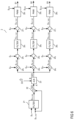
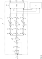
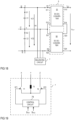
- Figure 1 shows a circuit diagram of a power converter 10 known as Vienna rectifier, which is a switched-mode three-phase (3 ⁇ ) AC-DC power converter.
- the power converter includes an input with three input nodes A, B, C each configured to receive a respective one of three input voltages V1, V2, V3, two DC link nodes X, Z configured to provide a DC link voltage V4 therebetween, and a midpoint Y coupled to each of the two DC link nodes X, Z.
- Each of the three input voltages V1, V2, V3 is a voltage between the respective input node A, B, C and a common ground node N.
- the power converter further includes three inductors L1, L2, L3 each coupled to a respective one of the three input nodes A, B, C.
- the inductors L1, L2, L3 are directly coupled to the inputs A, B, C. This, however is only an example. According to another example (not shown) an input filter is connected between the inputs A, B, C and the inductors L1, L2, L3.
- the power converter further includes a rectifier bridge 1 with three bridge legs 1 1 , 1 2 , 1 3 .
- Each of the three bridge legs 1 1 1 , 1 2 , 1 3 which are only schematically illustrated in Figure 1 , includes at least one electronic switch Q1, Q2, Q3 and is connected to a respective one of the three inductors L1, L2, L3, so that each of the bridge legs 11, 12, 13 is coupled to a respective one of the three inputs A, B, C through a respective one of the three inductors L1, L2, L3.
- each of the three bridge legs 1 1 , 1 2 , 1 3 is connected to the two DC link nodes X, Z and the midpoint Y.
- the midpoint Y may be coupled to a first one X of the two DC link nodes X, Z via a first capacitor C1 and to a second one Z of the two DC link nodes X, Z via a second capacitor C2.
- a voltage VC1 across the first capacitor C1 is referred to as first capacitor voltage and a voltage VC2 across the second capacitor C2 is referred to as second capacitor voltage in the following.
- the input voltages V1, V2, V3 received by the power converter are alternating input voltages such as sinusoidal input voltages.
- a phase shift between each pair of these input voltages V1, V2, V3 may be 120°.
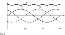
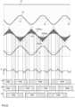
- Figure 2 shows signal diagrams of sinusoidal input voltages V1, V2, V3 during one period of each of these input voltages V1, V2, V3.
- a phase shift between each pair of these input voltages V1-V3 is 120° (2 ⁇ /3) in this example.
- Each of the three sinusoidal input voltages V1-V3 periodically changes between a minimum voltage level and a maximum voltage level, wherein the maximum voltage level is a positive voltage level and the minimum voltage level is a negative voltage level in this example.
- a magnitude of the minimum level essentially equals a magnitude of the maximum level and the three input voltages V1-V3 have essentially the same minimum voltage levels and the same maximum voltage levels. Further, the three input voltages V1-V3 may have essentially the same frequency, wherein this frequency is between 50 Hz and 60 Hz, for example.
- Figure 2 illustrates the input voltages V1, V2, V3 dependent on a phase angle.
- the plurality of the input voltages V1, V2, V3 is also referred to as input voltage system.
- a magnitude A1, A2, A3 of the maximum voltage level and the minimum voltage level of each of the input voltages V1, V2, V3 may also be referred to as amplitude of the respective input voltage V1, V2, V3.
- one of the three input voltages has the highest (positive) voltage level of the three input voltages V1, V2, V3 and one of the three input voltages has the lowest (negative) voltage level of the three input voltages V1, V2, V3, wherein in each period each of the three input voltages V1, V2, V3 has the highest level and each of the three input voltages V1, V2, V3 has the lowest level for a certain time period.
- a difference between the highest voltage level and the lowest voltage level is referred to as line-to-line voltage V LL .
- the line-to-line voltage V LL associated with the input voltages V1, V2, V3 shown in Figure 2 is also illustrated in Figure 2 .
- the line-to-line voltage is periodic, wherein the duration of one period of the line-to-line voltage V LL is 1/6 of a duration of one period of the input voltages V1, V2, V3.
- one period of the input voltages V1, V2, V3 includes phase angles from 0° to 360° (0 to 2 ⁇ ) and one period of the line-to-line voltage V LL ranges over 60° of one period of the input voltages V1, V2, V3.
- V LL_MAX A ⁇ 3 .
- Operating a power converter of the type shown in Figure 1 may include (a) regulating the DC link voltage V4 such that it has a predefined voltage level, and (b) regulating each of the three input currents I1, I2, I3 such that it has a current waveform that essentially equals the waveform of the respective input voltage V1, V2, V3.
- these input currents I1, I2, I3 essentially have sinusoidal waveforms when the input voltages V1, V2, V3 are sinusoidal voltages.
- Regulating each of the input currents I1, I2, I3 may include regulating an inductor voltage VL1, VL2, VL3 across the respective inductor L1, L2, L3, wherein regulating the inductor voltages VL, VL2, VL3 may include regulating voltages VA', VB', VC' at circuit nodes A', B', C' arranged between the inductors L1, L2, L3 and the bridge legs 1 1 , 1 2 , 1 3 .
- circuit nodes A', B', C' are referred to as switch nodes of the bridge legs 1 1 , 1 2 , 1 3 , and the voltages VA', VB', VC' at these switch nodes A', B', C', are referred to as switch node voltages in the following, wherein these voltages VA', VB', VC' are referenced to the common ground node N.
- switch node voltages in the following, wherein these voltages VA', VB', VC' are referenced to the common ground node N.
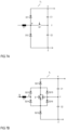
- Figure 3 illustrates a power converter of the type illustrated in Figure 1 , wherein the bridge legs 1 1 , 1 2 , 1 3 are implemented in accordance with one specific example. (Further examples for implementing the inductor voltages VL1, VL2, VL3 are explained herein further below.)
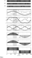
- Figure 4 illustrates signal diagrams of signals occurring in the power converter during one period of the input voltages V1, V2, V2.
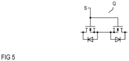
- each of the bridge legs 1 1 1 , 1 2 , 1 3 includes an electronic switch Q1, Q2, Q3 connected between the respective switch node A', B', C' and the midpoint Y, a first rectifier element D11, D21, D31 connected between the respective input node A', B', C' and the first DC link node X, and a second rectifier element D12, D22, D32.
- the electronic switches Q1, Q2, Q3 may be implemented as bidirectional blocking switches.
- a "bidirectional blocking switch” is a switch that is capable of blocking a current independent of a polarity of a voltage applied to the electronic switch.
- the electronic switch Q (wherein Q represents an arbitrary one of switches Q1, Q2, Q3) includes two MOSFETs (Metal Oxide Semiconductor Field Effect Transistors) that are connected in series such that integrated body diodes are connected in a back-to-back configuration. That is, these MOSFETs are connected in series such that the body diodes integrated in these MOSFETs either have their anodes connected or have their cathodes connected.
- the two MOSFETs may be driven by the same drive signal S (wherein S represents an arbitrary one of the drive signals S1, S2, S3 received by the switches Q1, Q2, Q3).
- S represents an arbitrary one of the drive signals S1, S2, S3 received by the switches Q1, Q2, Q3
- the first and second rectifier elements D1 1-D32 may be implemented as passive rectifier elements such as diodes. This, however, is only an example. Active rectifier elements such as MOSFETs operated as synchronous rectifiers may be used as well.
- the first rectifier elements D11, D21, D31 are configured to enable a (positive) current flow from the respective switch node A', B', C' towards the first DC link node X and the second rectifier elements D12, D22, D32 are configured to enable a (positive) current flow from the second DC link node Z towards the respective switch node A', B', C'.
- the diodes forming the first rectifier elements D11, D21, D31 have their cathodes connected to the first DC link node X and have their anodes connected to the respective input node A', B', C'
- the diodes forming the second rectifier elements D12, D22, D32 have their anodes connected to the second DC link node Z and have their cathodes connected to the respective input node A', B', C'.
- controlling the current 11, 12, 13 through each of the inductors L1, L2, L3 includes controlling the voltage VL1, VL2, VL3 across the respective inductor L1, L2, L3.
- Each inductor voltage VL1, VL2, VL3 is given by the respective input voltage V1, V2, V3 minus the respective switch node voltage VA', VB', VC'.
- the input voltages V1, V2, V3 are predefined by a voltage source such as a power grid and can be measured, so that the inductor voltages VL1, VL2, VL3 and, therefore, the inductor currents 11, 12, 13 can be regulated by regulating the switch node voltages VA', VB', VC'. This is explained with reference to Figure 4 in the following.
- Figure 4 illustrates drive signals S1, S2, S3 of the electronic switches Q1, Q2, Q3, sinusoidal input voltages V1, V2, V3 and corresponding input currents 11, 12, 13, which are essentially sinusoidal.
- Figure 4 further illustrates currents ID11, ID12 through the first and second rectifier elements D11, D12 in a first one 1 1 of the bridge legs 1 1 , 1 2 , 1 3 , a current IQ1 through the electronic switch Q1 in the first bridge leg 1 1 , and a voltage VQ1 across the electronic switch Q1 in the first bridge leg 1 1 .
- the power converter is in a steady state in which the DC link voltage V4 has already reached a desired voltage level and that a power consumption of a load Z (illustrated in dashed lines in Figure 3 ) connected to the DC link nodes X, Z is constant.
- This load may be an arbitrary load, including a load that includes a further power converter.
- the power converter may be operated in a continuous conduction mode (CCM), that is, the inductor currents I1, I2, I3 do not decrease to zero during each of the positive and the negative halfwave of the respective input voltage V1, V2, V3. (The input currents I1, I2, I3 turn zero only for a short time period when the respective input voltage V1, V2, V3 crosses zero).
- CCM continuous conduction mode
- the "midpoint voltage” VY is the voltage at the midpoint Y, which is not directly connected to the ground node N, referenced to the ground node N.
- the midpoint voltage VY or the negative -VY of the midpoint voltage may also be referred to as common mode voltage VCM in the following.
- the common mode voltage VCM may be regulated such that it is zero, so that the potential at the midpoint equals the potential at the ground node.
- the common mode voltage VCM may be regulated such that it is different from zero and varies over one period of the input voltages V1, V2, V3.
- the inductor currents can be regulated such that each inductor current I1, I2, I3 is positive during the positive halfwave of the respective input voltage V1, V2, V3 and negative during the negative halfwave of the respective input voltage V1, V2, V3. Examples for regulating the common mode voltage VCM are explained in further detail herein below.
- Controlling the input currents I1, I2, I3 is explained in the following with reference to controlling the current I1 through a first one L1 of the inductors L1, L2, L3, which is the inductor connected to the first bridge leg 1 1 . Regulating the other two 12, 13 of the input currents I1, I2, I3 is achieved in the same way.
- first input the voltage V1 received at this input is referred to as first input voltage
- the switch node A' of the first bridge leg 1 1 is referred to as first switch node
- the inductor L1 connected to the first switch node A' is referred to as first inductor
- the voltage VL1 across the first inductor L1 is referred to as first inductor voltage VL1.
- the first inductor current 11 is positive, that is, the inductor current flows in a direction as indicated by the arrow in Figure 3 .
- the inductor current I1 flows through the first rectifier element D11 during the off-period of the first switch Q1, that is, after the first switch Q1 has been switched off.
- the voltage VA' at the first switch node A' is given by the voltage VX at the first DC link node X minus a voltage drop across the first rectifier element D11.
- This voltage drop across the first rectifier element is negligible so that during the off-period of the first electronic switch Q1, the potential at the first switch node A' is essentially clamped to the voltage VX at the first DC link node X.
- This voltage VX is referenced to the ground node and is referred to as first DC link node voltage in the following.
- the first inductor current I1 is negative, that is, the inductor current flows in a direction opposite the direction as indicated by the arrow in Figure 3 .
- the inductor current I1 flows through the second rectifier element D12 during the off-period of the first switch Q1.
- the potential at the first switch node A' is given by the voltage VZ at the second DC link node Z minus a voltage drop across the second rectifier element D12.
- This voltage drop across the second rectifier element is negligible so that during the off-period of the first electronic switch Q1, the potential at the first switch input node A' is essentially clamped to the voltage VZ at the second DC link node Z.
- This voltage VZ is referenced to the ground node and is referred to as second DC link node voltage in the following.
- the common mode voltage VCM can be positive and negative. In each case, the magnitude of the common mode voltage VCM is lower than the magnitude of each of the first and second capacitor voltages, so that the first DC link node voltage VX is positive and the second DC link node voltage VZ is negative.
- the inductor current I1 increases when the inductor voltage VL1 is positive, and decreases when the inductor voltage VL1 is negative, and remains constant when the inductor voltage VL1 is zero.
- the voltage VA' at the first switch node A' between two of these three voltage levels VX, VY, VZ the first input current I1 can be generated such that it follows a sinusoidal waveform.
- the inductor current I1 increases, when the average of the inductor voltage VL1 over one-period and one off-period of the first switch Q1 is positive and decreases when the average of the inductor voltage VL1 over one-period and one off-period of the first switch Q1 is negative.
- the electronic switch Q1 (as well as the other switches Q2, Q3) may be operated in a pulse-width modulated (PWM) fashion at a fixed switching frequency fsw, which is significantly higher than the frequency of the first input voltage V1.
- the switching frequency fsw is between several kHz and several 10 kHz and may range up to several 100 kHz, for example.
- of the duty cycle d1 is given by the ratio between the duration T OFF of the off-period and the duration T of the drive cycle,
- T OFF T .
- the duty cycle d1 can be positive or negative, wherein the duty cycle d1 is positive during the positive halfwave of the first input voltage V1 and negative during the negative halfwave of the first input voltage V1.
- a positive duty cycle d1 different from one (1) or zero (0) represents a ratio between the duration of the on-period and the off-period in a drive cycle in the positive halfwave of the first input voltage V1.
- a negative duty cycle d1 different from 1 or zero represents a ratio between the duration of the on-period and the off-period in a drive cycle in the negative halfwave of the first input voltage V1.
- the first switch node voltage VA' is obtained by switching between the first DC link node voltage VX and the midpoint voltage VY, or between the second DC link node voltage VZ and the midpoint voltage VY.
- the first switch node voltage A' is therefore given by the average voltage at the first switch node A' in one drive cycle.
- the duty cycle d1 of the first electronic switch Q1 the first switch node voltage VA' and, therefore, the first inductor voltage VL1 can be adjusted.
- the duty cycle d1 can be calculated.
- the duty cycle d1 is given by the ratio between the duration T OFF of the off-period and the duration T of one drive cycle, and the duty cycle d1 is positive in the positive halfwave of the first input voltage V1 and negative in the negative halfwave of the first input voltage V1.
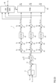
- the power converter includes a control circuit 2 that is configured to operate the at least one electronic switch Q1, Q2, Q3 in each of the bridge legs 1 1 , 1 2 , 1 3 . More specifically, this control circuit 2 may be configured to generate drive signals S1, S2, S3 received by the electronic switches Q1, Q2, Q3 such that the DC link voltage V4 has a predefined voltage level and such that the inductor currents (the input currents) I1, I2, I3 essentially have the same waveform as the input voltages V1, V2, V3.
- the control circuit 2 receives a DC link voltage signal S V4 , wherein the DC link voltage signal S V4 represents the DC link voltage V4.
- the DC link voltage V4 may be measured in a conventional way by any kind of voltage measurement circuit (not shown) in order to obtain the DC link voltage signal S V4 .
- the control circuit 2 receives input voltage signals S V1 , S V2 , S V3 , each representing a respective one of the input voltages V1, V2, V3 and input current signals S I1 , S I2 , S I3 each representing a respective one of the input currents I1, I2, I3.
- the input voltage V1, V2, V3 may be measured in a conventional way in order to obtain the input voltage signals S V1 , S V2 , S V3 . Further, the input currents I1, I2, I3 may be measured in a conventional way in order to obtain the input current signals S I1 , S I2 , S I3 .
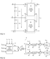
- One example of a control circuit 2 configured to generate the drive signals S1-S3 is illustrated in Figure 6 .
- the control circuit 2 shown in Figure 6 includes a first filter 21 that receives the DC link voltage signal S V4 and a DC link voltage reference signal S V4_REF , wherein the DC link voltage reference signal S V4_REF represents the desired voltage level of the DC link voltage V4.
- the filter 21 subtracts the DC link voltage reference signal S V4_REF from the DC link voltage signal S V4 and filters the difference in order to generate a DC link voltage error signal S V4_ERR .
- the filter (or controller) may have one of a proportional (P) characteristic, a proportional-integrative (PI) characteristic, a proportional-integrative-derivative (PID) characteristic, or the like.
- a multiplier 22 receives the DC link voltage error signal S V4_ERR and the DC link voltage reference signal S V4_REF , wherein an output signal S22 of the multiplier 22 represents a desired output power of the power converter.
- a divider 23 divides the multiplier output signal S22 by a signal that represents 1.5 times the square of the amplitude of the input voltages V1, V2, V3 ( 3 2 ⁇ V ⁇ 2 ).
- An output signal S23 of the divider 23 represents an overall desired input current of the power converter, wherein the overall desired input current is the input current that is required by the power converter in order to achieve the desired voltage level of the DC link voltage V4 as defined by the DC link voltage reference signal S V4_REF .
- the control circuit 2 further includes three branches, wherein each of these branches receives the divider output signal S23 and generates a respective one of the three drive signals S1, S2, S3.
- Each of these branches includes a multiplier 24i, 24 2 , 24 3 that multiplies the divider output signal S23 with the respective input voltage signal S V1 , S V2 , S V3 , wherein an output signal of each of these multipliers 24i, 24 2 , 24 3 is an input current reference signal S I1_REF , S I2_REF , S I3_REF , that is, each of these signals S I1_REF , S I2_REF , S L ⁇ _REF represents the desired current level of a respective one of the input currents I1, I2, I3.
- each of these subtractors 25 1 , 25 2 , 25 3 is filtered by a respective filter 26 1 , 26 2 , 26 3 connected downstream the respective subtractor 25 1 , 25 2 , 25 3 , wherein an output signal S VL1_REF , S VL2_REF , S VL3_REF of the respective filter 26 1 , 26 2 , 26 3 represents a desired voltage level of a respective one of the three inductor voltages VL1, VL2, VL3.
- a further subtractor 27 1 , 27 2 , 27 3 subtracts the input voltage signal S V1 , S V2 , S V3 from the respective inductor voltage reference signal S VL1_REF , S VL2_REF , S VL3_REF in order to obtain switch node voltage reference signals S VA'_REF , S VB'_REF , S VC'_REF , wherein each of these switch node voltage reference signals S VA'_REF , S VB'_REF , S VC'_REF represents the desired voltage level of a respective one of the three leg input voltages VA', VB', VC'.
- each of the three branches that generate the drive signals S1, S2, S3 includes a PWM modulator 28 1 , 28 2 , 28 3 that receives a respective one of the leg input voltage reference signals S VA'_REF , S VB'_REF , S VC'_REF , wherein each of these modulators 28 1 , 28 2 , 28 3 is configured to generate a respective one of the drive signals S1, S2, S3 based on the respective reference signal S VA'_REF' , S VB'_REF , S VC'_REF such that in each drive cycle of the at least one electronic switch Q1, Q2, Q3 an average of the respective leg input voltage VA', VB', VC' equals the voltage level as defined by the respective leg input voltage reference signal S VA'_REF' , S VB'_REF' , S VC'_REF .
- the specific implementation of the PWM modulators 28 1 , 28 2 , 28 3 is dependent on the type of a bridge
- each of the PWM modulators 28 1 , 28 2 , 28 3 may be configured to calculate the duty cycles d1, d2, d3 of the drive signals S1, S2, S3 based on one of equations (3a), (3b) or (3c) and generate the drive signals S1, S2, S3 in accordance with the calculated duty cycle.
- the duty cycles d1, d2, d3 not only the switch node voltages VA', VB', VC' but also the common mode voltage VCM can be adjusted.
- the first DC link node voltage VX has to be equal to or higher than the highest voltage level of the three input voltages V1, V2, V3 and the second DC link node voltage VZ has to be equal to or lower than the lowest voltage level of the three input voltages V1, V2, V3.
- the common mode voltage VCM is zero
- each of the capacitor voltages VC1, VC2 has to be higher than the amplitude of the three input voltages.
- the switch node voltages VA', VB', BC' follow the input voltages V1, V2, V3 and can be considered to be essentially equal to the input voltages V1, V2, V3 (the inductor voltages VL1, VL2, VL3 are low as compared to the input voltages V1, V2, V3).
- the PWM modulators 28 1 , 28 2 , 28 3 may each receive a common mode voltage signal S VCM that represents the desired common mode voltage.
- This common mode signal S VCM may be provided by a central controller (which is not illustrated). This central controller may be a microcontroller or the like.
- the electronic switch Q1, Q2, Q3 in each of the bridge legs 11, 12, 13 is operated in the PWM mode throughout the period of the input voltages V1, V2, V3.
- This type of operating mode will also be referred to as 3/3 mode in the following.
- the bridge legs 1 1 1 , 1 2 , 1 3 can be implemented in various ways. Some examples for implementing the individual bridge legs 1 1 -1 3 are explained with reference to the first bridge leg 1 1 in the following.
- the second and third bridge leg 1 2 . 1 3 can be implemented in the same way as the first bridge leg 1 1 .
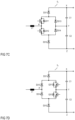
- Figure 7A illustrates a first example of the first bridge leg 1 1- In this example, the first bridge leg 1 1 is implemented in the way explained with reference to Figure 3 .
- the bridge leg 1 1 includes a bidirectional blocking switch Q1 connected between the first switch node A' and the midpoint Y, a first rectifier element D11 connected between the first switch node A' and the first DC link node X, and a second rectifier element D12 connected between the second DC link node Z and the first switch node A'.
- the bridge leg 1 1 includes a first rectifier element D211 connected to the first DC link node X, a second rectifier element D212 connected to the second DC link node Z, a third rectifier element D213 connected between the switch node A' and the first rectifier element D21 1, a fourth rectifier element D214 connected between the switch node A' and the second rectifier element D212, a fifth rectifier element D215 connected between the midpoint Y and the first rectifier element D211, and a sixth rectifier element D216 connected between the midpoint Y and the second rectifier element D212.
- an electronic switch Q1 is connected between the first and second rectifier elements D211, D212.
- This electronic switch Q1 may be a unidirectional electronic switch such as, for example, a MOSFET.
- the rectifier elements D211-D216 may be implemented as diodes. These rectifier elements D211-D216 are connected such that during the positive halfwave of the first input voltage V1, the inductor current I1 can flow from the first switch node A' via the third rectifier element D213, the electronic switch Q1 and the sixth rectifier element D216 to the midpoint Y, when the electronic switch Q1 is switched on. When the electronic switch Q1 is switched off, the inductor current I1 flows via the third rectifier element D213 and the first rectifier element D211.
- the current flows from the midpoint Y via the fifth rectifier element D215 and the fourth rectifier element D214 to the first switch node A' when the electronic switch Q1 is switched on.
- the current flows from the second DC link node Z via the second rectifier element D212 and the fourth rectifier element D214 to the first switch node A'.
- Figure 7C shows a third example of the first bridge leg 1 1 .
- the first bridge leg 1 1 includes a first rectifier element D311 connected to the first DC link node X, a second rectifier element D312 connected to the second DC link node Z, a first switch Q311 connected between the first switch node A' and the first rectifier element D311, a second switch Q312 connected between the first switch node A' and the second rectifier element D312, a third rectifier element D313 connected between the midpoint Y and the first rectifier element D31 1, and a fourth rectifier element D314 connected between the midpoint Y and the second rectifier element D312.
- the electronic switches Q311, Q312 may be unidirectional blocking switches such as, for example, MOSFETs.
- the electronic switches Q311, Q312 and the rectifier elements D311-D314 may be connected such that during the positive halfwave of the input voltage V 1 the inductor current 11 flows via the switch node A' via the second electronic switch Q312 and the fourth rectifier element D314 to the midpoint Y when the second electronic switch Q312 is switched on.
- the inductor current I1 flows via the first electronic switch Q311 and the first rectifier element D311 to the first DC link node X.
- the first electronic switch Q311, Q312 may be switched on and off at the same time.
- the inductor current I1 flows via the body diode of the MOSFET forming the first electronic switch Q311 and the first rectifier element D311.
- the first and second electronic switch Q311, Q312 are operated in a complementary fashion, so that only one of the switches is switched on at the same time.
- the first switch Q311 is switched on when the second switch Q312 switches off, so that the inductor current I1 flows via the switched on first electronic switch Q311 and the first rectifier element D311.
- the inductor current I1 flows from the midpoint Y via the third rectifier element D311 and the first electronic switch Q311 to the first switch node A' when the first electronic switch Q311 is switched on.
- the inductor current I1 flows from the second DC link node Z via the second rectifier element D311 and the second electronic switch Q312 to the first switch node A'.
- Figure 7D shows a modification of the bridge leg 11 shown in Figure 7C .
- the first switch Q311 is connected between the midpoint Y and the first rectifier element D311
- the second switch Q312 is connected between the midpoint Y and the second rectifier element D312
- the third rectifier element D313 is connected between the switch node A' and the first rectifier element D311
- the fourth rectifier element D314 is connected between the switch node A' and the second rectifier element D311.
- Each of the bridge legs 1 1 shown in Figures 7A, 7B , 7C and 7D is configured to provide three different voltage levels at the first switch node A'.
- the average electrical potential at the first switch node A' during one drive cycle is generated from two voltage levels, the electrical potential VX at the first DC link node X and the electrical potential VY at the midpoint Y during the positive halfwave at the input voltage V1, and the electrical potential VZ at the second DC link node Z and the electrical potential VY at the midpoint Y during the negative halfwave of the input voltage V1.
- FIGS 7E and 7F illustrate further examples of the first bridge leg 1 1 .
- the bridge leg 1 1 includes capacitors in addition to DC link capacitors C1, C2.
- the bridge legs 1 1 illustrated in Figures 7D and 7E are so-called multi-level bridge legs, wherein the bridge leg 1 1 shown in Figure 7D is a Hybrid Active Neutral Point Clamped Converter leg, and the bridge leg 1 1 shown in Figure 7E is a Stacked Multicell Converter leg. These legs are known (see, for example, G. Gateau, T.A. Meynard, H.
- each of these bridge legs is capable of providing more than three different voltage levels, that is, the three voltage levels VX, VY, VZ and additional voltage levels for generating the switch node voltage VA'.
- the rectifier elements may be implemented as diodes (as illustrated). This, however, is only an example. According to another example (not shown) these rectifier elements may be implemented as synchronous rectifier elements.
- operating a power converter of the type illustrated in Figures 1 and 3 may include a PWM (pulse-width modulated) operation of each of the at least one electronic switch in each of the bridge legs 1 1 , 1 2 , 1 3 at each time of the operation.
- PWM pulse-width modulated
- Operating the switches Q1, Q2, Q3 in a PWM mode is associated with switching losses.
- Switchching losses are losses that occur in context with switching on and switching off the respective switch Q1, Q2, Q3. In order to increase the efficiency of the power converter it is desirable to reduce those switching losses.
- reducing switches losses includes operating the power converter in a reduced switching mode, wherein operating the power converter in a reduced switching mode includes deactivating the at least one switch Q1, Q2, Q3 in one or two of the bridge legs 1 1 , 1 2 , 1 3 for a time period that is significantly longer than the duration T of one drive cycle.
- deactivating the at least one switch includes deactivating the at least one switch for more than 10, more than 100 or even more than 1000 drive cycles.
- a bridge leg in which the at least one switch is deactivated is referred to as deactivated bridge leg.
- the "at least one electronic switch" of a bridge leg 1 1 , 1 2 , 1 3 may include one electronic switch or several electronic switches.
- a bridge leg 1 1 with one electronic switch is illustrated in Figure 7A wherein, as illustrated in Figure 5 , one switch may include two transistors.
- Bridge legs 1 1 with several (unidirectional blocking) switches are illustrated in Figures 7B-7F .
- “deactivating the at least one switch” includes deactivating each of the several switches.
- “the at least one electronic switch” is a switch that is used in a respective bridge leg to connect the switch node to the midpoint Y or to a circuit node having a voltage between the voltage at the midpoint Y and one of the first and second DC link node voltages VX, VZ.
- Voltages between the voltage at the midpoint Y and one of the first and second DC link node voltages VX, VZ are provided in the bridge legs illustrated in Figures 7E and 7F , for example.
- the rectifier elements that couple the switch nodes A', B', C' to the first and second DC link nodes X, Z may include an electronic switch.
- "deactivating the at least one switch” does not include deactivating electronic switches acting as (synchronous) rectifiers.
- Figure 8 illustrates signal diagrams of the drive signals S1, S2, S3, the input voltages V1, V2, V3, the DC link voltage V4, the input currents 11, 12, 13, the currents ID11, ID12, IQ11 in the first bridge leg 1 1 and the voltage VQ1 across the first switch Q1 in the first bridge leg 1 1 .
- the operating mode illustrated in Figure 8 is referred to as 1/3 mode in the following.
- a bridge leg in which the at least one electronic switch is operated in the PWM mode is referred to as "activated bridge leg”
- a bridge leg in which the at least one electronic switch is deactivated is referred to as “deactivated bridge leg” although a current may of course flow in the deactivated bridge leg between the respective switch node and one of the first and second DC link nodes X, Z.
- the power converter is operated in the 1/3 mode throughout the period of the input voltages V1, V2, V3. That is, at each time of the period of the input voltages V1, V2, V3 only one of the bridge legs 1 1 , 1 2 , 1 3 is activated and the other two bridge legs are deactivated.
- This type of operating mode is referred to as full 1/3 mode in the following. This, however, is only an example. According to another example explained further below it is also possible to operate the power converter such that only in some time periods (at some phase angles of one period of the input voltages V1, V2, V3) it operates in the 1/3 mode.
- the switch node voltage of a deactivated bridge leg is either clamped to the DC link voltage VX at the first DC link node X or the DC link voltage VZ at the second DC node Z.
- the switch node voltage of one bridge leg is clamped to the first DC link node voltage VX, and the switch node voltage of another bridge leg is clamped to the second DC link node voltage VZ.
- the bridge legs that are deactivated change over one period of the input voltage system. This is explained with reference to signal diagrams illustrated in Figure 13 herein further below..
- the currents through the two inductors that are connected to the deactivated bridge legs are regulated by suitably regulating the DC link voltage V4 by a further power converter 5 connected to the DC link nodes X, Z of the power converter.
- a power converter arrangement with a power converter of the type explained before and a further power converter 5 connected to the DC link nodes X, Z of the power converter is illustrated in Figure 10 .
- the power converter 10 is also referred to as first power converter and the further power converter 5 is also referred to as second power converter in the following.
- the second power converter 5 may be configured to provide a constant output current I OUT or a constant output voltage V OUT different from the DC link voltage V4.
- the second power converter 5 contributes to the regulation of the inductor currents 11, 12, 13 in the first power converter 10 by suitably regulating the DC link voltage V4 there is no increase of the losses occurring in the second power converter 5.
- the switching losses in the first power converter are significantly reduced. Thus, there is a synergy between the control of the first power converter and the control of the second power converter 5.
- control circuit 4 configured to operate a power converter arrangement with a first power converter and a second power converter of the type shown in Figure 9 is illustrated in Figure 10 .
- the control circuit 4 shown in Figure 10 includes two main branches (or subcircuits), a first branch 40 configured to operate the first power converter and a second branch 6 configured to operate the second power converter 5.
- the block diagram shown in Figure 10 illustrates the functional blocks of the control circuit 4 rather than a specific implementation. Those functional blocks can be implemented in various ways. According to one example, these functional blocks are implemented using dedicated circuitry. According to another example, the control circuit 4 is implemented using hardware and software.
- the first control circuit includes a microcontroller and software executed by the microcontroller.
- the output current I OUT of the second power converter 5 is regulated and that the output voltage V OUT is defined by a load (not shown) receiving the output current.
- the load may be a battery that receives the output current I OUT and defines the output voltage V OUT .
- the first branch 40 of the control circuit 4 shown in Figure 10 is based on the control circuit shown in Figure 6 , wherein the same elements have the same reference characters.
- the control circuit 4 receives an output current signal S IOUT wherein the output current signal S IOUT represents the output current I OUT .
- the output current I OUT may be measured in a conventional way by any kind of current measurement circuit (not shown) in order to obtain the output current signal S IOUT .
- the control circuit 4 includes a first filter 41 that receives the output current signal S IOUT and an output current reference signal S IOUT REF , wherein the an output current reference signal S IOUT REF represents the desired current level of the output current I OUT .
- the first filter 41 subtracts the output current reference signal S IOUT REF from the output current signal S IOUT , for example, and filters the difference in order to generate an output signal S V51_REF .
- this output signal S V51_REF represents a desired voltage V51 across an inductor 51 in the second power converter 5, wherein this inductor 51 carries the output current I OUT .
- FIG. 9 One example of such inductor 51 is illustrated in Figure 9 .
- the filter may have one of a proportional (P) characteristic, a proportional-integrative (PI) characteristic, a proportional-integrative-derivative (PID) characteristic, or the like.
- a adder 42 receives the filter output signal S V51_REF and an output voltage signal S VOUT that represents the output voltage V OUT , wherein an output signal S42 of the adder 42 and the filter output signal S V51_REF are received by a multiplier.
- An output signal S43 of the multiplier 43 represents a desired output power of the power converter arrangement.
- the divider 23 already explained with Figure 6 divides the multiplier output signal S43 by a signal that represents 1.5 times the square of the amplitude of the input voltages V1, V2, V3 ( 3 2 ⁇ V ⁇ 2 ).
- An output signal S23 of the divider 23 represents an overall desired input current of the first power converter.
- the divider output signal S23 is processed by the three branches explained with reference to Figure 6 before in order to generate the three switch node voltage reference signals S VA'_REF , S VB'_REF , S VC'_REF .
- the current control loop is the slowest one of the control loops explained in context with Figure 10 .
- Controlling the output current I OUT by the control circuit 4 is only an example.
- the output voltage V OUT is controlled.
- the filter 41 receives the output voltage signal S VOUT and an output voltage reference signal S VOUT_REF representing the desired voltage level of the output voltage V OUT .
- the adder 42 is omitted and the multiplier 43 receives the output signal from the filter 41 and the output voltage reference signal S VOUT_REF .
- a PWM modulator 44 receives the switch node voltage reference signals S VA'_REF , S VB'_REF , S VC'_REF . From these switch node voltage reference signals S VA'_REF , S VB'_REF , S VC'_REF the PWM modulator 44 (a) selects a maximum and deactivates the bridge leg associated with the maximum voltage reference signal; (b) selects a minimum and deactivates the bridge leg associated with the minimum voltage reference signal; and (c) operates the remaining bridge leg in the PWM mode.
- the "remaining bridge leg" is the bridge leg, associated with the switch node reference signal that is between the maximum and the minimum switch node voltage reference signal. This switch node voltage reference signal is referred to as intermediate switch node voltage reference signal in the following.
- the second branch 6 of the control circuit also receives the three switch node voltage reference signals S VA'_REF , S VB'_REF , S VC'_REF and is configured to control operation of the second power converter 5 based on these signals S VA'_REF , S VB'_REF , S VC'_REF .
- S VA'_REF switch node voltage reference signals
- S VB'_REF switch node voltage reference signals
- Figure 11 illustrates one example of the second power converter 5.
- the second power converter 5 includes a first converter stage 51 and a second converter stage 52, wherein each of these a first and second converter stages 51, 52 includes a first input node 511, 521, a second input node 512, 522, a first output node 513, 523, and a second output node 514, 524.
- the first input node 511 of the first converter stage 51 may be connected to the first DC link node X
- the second input node 522 of the second converter stage 52 may be connected to the second DC link node Z
- the second input node 512 of the first converter stage 51 and the first input node 521 of the second converter stage 52 may be connected with each other and connected to the midpoint Y.
- the second output node 514 of the first converter stage 51 and the first output node 523 of the second converter stage 52 may be connected with each other.
- the output voltage V OUT is the voltage between the first output node 513 of the first converter stage 51 and the second output node 524 of the second converter stage 52.
- the converter stages 51, 52 may each be implemented with one of various different converter topologies.
- each of the converter stages 51, 52 is implemented as an isolated DC-DC converter, that is, a DC-DC converter that includes a transformer between the respective input 511, 512 or 521, 522 and the respective output 513, 514 or 523, 534.
- each of the converter stages 51, 52 is implemented as a non-isolated DC-DC converter, that is, a DC-DC converter that does not include a transformer between the respective input 511, 512 or 521, 522 and the respective output 513, 514 or 523, 534.
- Examples of different types of DC-DC converters that are suitable to be used as first and second converter stage 51, 52 include, but are not restricted to: a flyback converter (isolating), an LLC converter (isolating), dual active bridge (DAB) converter (isolating), a phase-shifted full bridge converter (isolating), a buck-boost converter, a boost-buck converter, etc.
- a flyback converter Isolating
- an LLC converter Isolating
- DAB dual active bridge
- phase-shifted full bridge converter isolating
- buck-boost converter a boost-buck converter
- This control circuit 6 includes a maximum and minimum selector 61 that receives the three switch node voltage reference signals S VA'_REF , S VB'_REF , S VC'_REF .
- the first signal S MAX ' is also referred to as maximum switch node voltage reference signal S MAX ', and the second signal S MIN ' is also referred to as minimum switch node voltage reference signal.
- the intermediate switch node voltage reference signal is also referred to as S INT ' in the following.
- the second control circuit branch 6 is configured to operate the second power converter 5 in such a way that the DC link voltage V4 equals a voltage that is represented by the difference between the maximum switch node voltage reference signal S MAX ' and the minimum switch node voltage reference signal S MIN '. Referring to the above, the switch nodes of the bridge legs that are deactivated are clamped to the first DC link node voltage VX and the second DC link node voltage VZ, respectively.
- the switch nodes that are clamped to the first and second DC link nodes X, Z receive the switch node voltages calculated by the first control circuit branch 40.
- the inductor currents of those inductors connected to deactivated bridge legs have a current level as represented by the respective input current reference signal calculated by the first control circuit branch 40.
- the second control circuit branch 6 includes a subtractor 62 that subtracts the minimum switch node voltage reference signal S MIN from the maximum switch node voltage reference signal S MAX ', wherein a multiplier 63 multiplies an output signal of the subtractor with 0.5.
- An output signal of the multiplier forms a first capacitor voltage reference signal S VC1_REF and a second capacitor voltage reference signal S VC2_REF , wherein the first capacitor voltage reference signal S VC1_REF represents a desired value of the first capacitor voltage VC1, and the second capacitor voltage reference signal S VC2_REF represents a desired value of the second capacitor voltage VC2.
- the second control circuit branch 6 includes a first branch and a second branch.
- the first branch receives the first capacitor voltage reference signal S VC1_REF and is configured to provide a first input current reference signal S I51_REF , wherein the first input current reference signal S I51_REF represents a desired input current 151 of the first converter stage 51.
- the second branch receives the second capacitor voltage reference signal S VC2_REF and is configured to provide a second input current reference signal S I52_REF , wherein the second input current reference signal S I52_REF represents a desired input current 152 of the second converter stage 52.
- the first branch includes a subtractor 64 1 that subtracts a first capacitor voltage signal S CV1 , which represents the first capacitor voltage VC1, from the first capacitor voltage reference signal S VC1_REF .
- An output signal of the subtractor is filtered by a filter 65i, wherein an output signal S IC1_REF of the filter represents a desired current level of a current into the first capacitor C1.
- the first input current reference signal S I51_REF is given by a difference between a current signal Six that represents a current into the first DC link node X (wherein this current IX is provided by the first power converter) and the filter output signal S IC1_REF .
- the second branch includes a subtractor 64 2 that subtracts a second capacitor voltage signal S CV2 , which represents the second capacitor voltage VC2, from the second capacitor voltage reference signal S VC2_REF .
- An output signal of the subtractor is filtered by a filter 65 2 , wherein an output signal S IC2_REF of the filter represents a desired current level of a current into the second capacitor C2.
- the second input current reference signal S I52_REF is given by a difference between a current signal Siz that represents a current into the second DC link node Z (wherein this current IZ is provided by the first power converter) and the filter output signal S IC2_REF .
- a first PWM modulator 67 1 receives the first input current reference signal S I51_REF and a first input current signal S I51 , wherein the latter represents the first input current 151, and is configured to control operation of one or more switches (not shown in the figures) included in the first converter stage 51 such that the first input current 151 has a current level as represented by the first input current reference signal S I51_REF .
- a second PWM modulator 67i receives the second input current reference signal S I52_REF and a second input current signal S I52 , wherein the latter represents the second input current 152, and is configured to control operation of one or more switches (not shown in the figures) included in the second converter stage 52 (not shown in the figures) such that the first input current 151 has a current level as represented by the first input current reference signal S I51_REF .
- the specific implementation of the PWM modulators 67 1 , 67 2 is dependent on the specific type of power converter used to implement the first and second converter stages 51, 52. However, PWM modulators configured to control the input current in various kinds of DC-DC converters are known, so that no further explanations are required in this regard.
- activating one of the three bridge legs 1 1 , 1 2 , 1 3 and deactivating the two other bridge legs 1 1 , 1 2 , 1 3 by the PWM modulator 44 in the 1/3 mode is dependent on the switch node voltage reference signals S VA'_REF , S VB'_REF , S VC'_REF .
- Time instances at which two of these switch node voltage reference signals S VA'_REF , S VB'_REF , S VC'_REF are equal can be neglected, so that at each time, from these switch node voltage reference signals S VA'_REF , S VB'_REF , S VC'_REF , one forms the maximum switch node voltage reference signal S MAX ', one forms the intermediate switch node voltage reference signal S INT ', and one forms the minimum switch node voltage reference signal S MIN '. This is explained with reference to Figure 13 in greater detail.
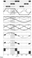
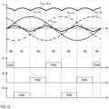
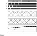
- Figure 13 illustrates signal diagrams of switch node voltage reference signals S VA'_REF , S VB'_REF , S VC'_REF , wherein each of these signals represents the desired voltage value of the respective switch node voltage VA', VB', VC'.
- Figure 13 further illustrates which of the bridge legs is operated in the PWM mode at which time or phase angle. Referring to the above and as illustrated in Figure 13 , in the steady state, each of the switch node voltage reference signals S VA'_REF , S VB'_REF , S VC'_REF follows the respective input voltage.
- a relationship between the individual switch node voltage reference signals S VA'_REF , S VB'_REF , S VC'_REF changes several times within one period.
- the "relationship" means the signal level of one of the switch node voltage reference signals S VA'_REF , S VB'_REF , S VC'_REF relative to the signal levels of the other two of the switch node voltage reference signals S VA'_REF , S VB'_REF , S VC'_REF .
- time periods P1-P6 which are also referred to as operating phases in the following, wherein in each of these time periods P1-P6 the relationship between the switch node voltage reference signals S VA'_REF , S VB'_REF , S VC'_REF does not change.
- the signal levels of the switch node voltage reference signals S VA'_REF , S VB'_REF , S VC'_REF vary in the individual operating phases P1-P6.
- the first switch node voltage reference signal S VA'_REF has the highest voltage level. That is, the voltage level of the first switch node voltage reference signal S VA'_REF is higher than the voltage level of a second one S VB'_REF of the switch node voltage reference signals S VA'_REF , S VB'_REF , S VC'_REF and the signal level of a third one S VC'_REF of the switch node voltage reference signals S VA'_REF , S VB'_REF , S VC'_REF . Further, in the first operating phase P1, the second switch node voltage reference signal S VB'_REF V2 hast the lowest voltage level.
- the voltage level of the second switch node voltage reference signal S VB'_REF is lower than the signal level of the first switch node voltage reference signal S VA'_REF and the signal level of the third switch node voltage reference signal S VC'_REF .
- the third switch node voltage reference signals S VA'_REF , S VB'_REF , S VC'_REF has a signal level between the voltage level of the first switch node voltage reference signal S VA'_REF and the signal level of the second switch node voltage reference signal S VB'_REF .
- the first switch node voltage reference signal S VA'_REF is the maximum switch node voltage reference signal S MAX '
- the second switch node voltage reference signal S VB'_REF is the minimum switch node voltage reference signal S MIN '
- the third switch node voltage reference signal S VC'_REF is the intermediate switch node voltage reference signal S INT ' _REF .
- the first switch node voltage reference signal S VA'_REF is the maximum switch node voltage reference signal S MAX '
- the second switch node voltage reference signal S VB'_REF is the intermediate switch node voltage reference signal S INT '
- the third switch node voltage reference signal S VC'_REF is the minimum switch node voltage reference signal S MIN ' _REF .
- the input voltage having the highest voltage level is referred to as maximum input voltage Vmax
- the input voltage having the lowest voltage level is referred to as minimum input voltage Vmin
- the input voltage having a voltage level between the highest voltage level and the lowest voltage level is referred to as intermediate input voltage V INT .
- the switch node voltage reference signals S VA'_REF , S VB'_REF , S VC'_REF in the steady state, essentially follow the input voltages V1, V2, V3, so that the output signal S MAX '- S MIN ' of the subtractor 62 shown in Figure 12 essentially represents the line-to-line voltage V LL .
- the subtractor output signal S MAX '- S MIN ' is also illustrated in Figure 13 .
- operating the power converter in the 1/3 mode includes activating the bridge leg associated with the intermediate voltage reference signal S INT ' and deactivating the bridge legs associated with the maximum switch node voltage reference signal S MAX ' and the minimum switch node voltage reference signal S MIN '. That is, in the first operating phase P1, for example, the third bridge leg 1 3 is activated, in the second operating phase P2 the second bridge leg 1 2 is activated, and so on.
- the bridge legs 1 1 1 , 1 2 , 1 3 are activated and deactivated by the PWM modulator 44 in the control circuit 4.
- a common mode voltage signal S VCM representing this common mode voltage V CM is also illustrated in Figure 13 over one period of the input voltages.
- dmax denotes the duty cycle of the bridge leg associated with the maximum switch node voltage reference signal S MAX ' in a respective operating phase
- dmin denotes the duty cycle of the bridge leg associated with the minimum switch node voltage reference signal S MIN ' in a respective operating phase
- Vmax' denotes the desired switch node voltage represented by the maximum switch node voltage reference signal
- Vmin' denotes the desired switch node voltage represented by the minimum switch node voltage reference signal S MIN '.
- the DC link voltage V4 is adjusted by the second converter 5 such that it equals Vmax'-Vmin', wherein Vmax' is the maximum of the desired switch node voltages and Vmin' is the minimum of the desired switch node voltages.
- Vmax' is the maximum of the desired switch node voltages
- Vmin' is the minimum of the desired switch node voltages.
- these desired switch node voltages Vmax', Vmin' essentially equal the maximum input voltage Vmax and the minimum input voltage Vmin, respectively, so that the varying DC link voltage V4 essentially equals the line-to-line voltage V LL .
- This is the lowest possible DC link voltage at which sinusoidal input currents 11, 12, 13 can be achieved, wherein the common mode voltage V CM is different from zero and given by equation (5) in this case.
- the power converter arrangement illustrated in Figure 9 is not restricted to generate the DC link voltage V4 such that it is defined by S MAX '-S MIN ' and essentially equals the line-to-line voltage V LL .
- a maximum selector 68 receives the subtractor output signal S62 and a minimum DC link voltage signal S V4_MIN , wherein the minimum DC link voltage signal S V4_MIN represents the minimum of the DC link voltage V4 that should be generated at the output of the first power converter 10.
- the maximum selector outputs the maximum of the two signal it receives to the multiplier 63.
- the voltage represented by the minimum DC link voltage signal S V4_MIN is referred to as minimum desired DC link voltage V4 MIN in the following.
- the DC link voltage V4 is generated such that it is generated based on the subtractor output signal S62 in time periods in which the subtractor output signal S62 is higher than the minimum desired DC link voltage signal S V4_MIN . In the remainder of the time the DC link voltage V4 is generated based on the minimum desired DC link voltage signal S V4_MIN .
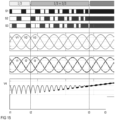
- the power converter is not operated in the 1/3 mode throughout each of the six operating phases anymore. Instead there are time periods in which the first power converter is operated in the 1/3 mode, but also time periods in which each of the bridge legs 1 1 , 1 2 , 1 3 operate in the PWM mode. This is illustrated between a second time instance t2 and a third time instance t3 in Figure 15 .
- the minimum desired DC link voltage V4 MIN is the minimum of the DC link voltage V4, which is also illustrated in Figure 15 .
- the duration in which the power converter operates in the 1/3 mode during one period of the input voltages V1, V2, V3 decreases as the minimum DC link voltage V4 MIN increases.
- the operating mode in which the power converter alternatingly operates in the 1/3 mode and the 3/3 mode is referred to as partial-boost mode in the following.
- the power converter When calculating the duty cycles d1, d2, d3 in accordance with equations (4a)-(4c), the power converter automatically changes between the 1/3 mode and the 3/3, because these duty cycles are dependent on the DC link voltage V4 that is adjusted by the second power converter 5.
- the common mode voltage V CM In the partial-boost mode, the common mode voltage V CM may be the same as in the full 1/3 mode. However, in those time periods in which the power converter, in the partial-boost mode, operates in the 3/3 mode the common mode voltage V CM may be different from the common mode voltage in the 1/3 mode. Only in the full 1/3 mode, the common mode voltage VCM is constrained to the value presented in equation (5).
- the degree of freedom that is available to adjust the common mode voltage VCM may be used to adjust the common mode voltage VCM such that a current IY into the midpoint is minimized. This is explained in detail herein further below.
- Figure 16 illustrates the different operating modes of the first power converter 10 dependent on the minimum desired DC link voltage signal S V4_MIN and the phase angle of the input voltages V1, V2, V3. More specifically, Figure 16 illustrates the different operating modes in an arbitrary one of the six operating phases P1-P6, wherein each of these operating phases covers 60° of one period of the input voltages V1, V2, V3.
- a phase angle of 0° represents the beginning of the respective operating phase
- a phase angle of 60° represents the end of the respective operating phase
- a phase angle of 30° represents the middle of the respective operating phase, which is when the intermediate input voltage in the respective operating phase crosses zero.
- the power converter operates in the full 1/3 mode when the minimum desired DC link voltage signal S V4_MIN is below a minimum of the subtractor output signal S62.
- the subtractor output signal S62 essentially represents the line-to-line voltage V LL , so that the power converter operates in the full 1/3 mode when the minimum desired DC link voltage V4 MIN is below the minimum line-to-line voltage V LL_MIN .
- the power converter operates in the partial-boost mode when the minimum desired DC link voltage signal S V4_MIN is between the minimum of the subtractor output signal S62 and a maximum of the subtractor output signal S62.
- the maximum of the subtractor output signal S62 essentially equals the maximum line-to-line voltage V LL_MAX , so that the power converter operates in the in the partial-boost mode when the DC link voltage V4 is between the minimum line-to-line voltage V LL_MIN and the maximum line-to-line voltage V LL_MAX .
- the portion of the operating phase in which the power converter operates in the 3/3 mode increases as the minimum desired DC link voltage V4 MIN increases and the portion of the operating phase in which the power converter operates in the 1/3 mode decreases as the minimum desired DC link voltage V4 MIN increases.
- the power converter operates in the full 3/3 mode when the minimum desired DC link voltage signal S V4_MIN is higher than the maximum of the subtractor output signal S62.
- the DC link voltage V4 is essentially constant and only dependent on the minimum desired DC link voltage signal S V4_MIN .
- the duty cycles d1, d2, d3 may be calculated based on equations (3a) and (3b) by the PWM modulator 44 in the control circuit 4.
- the second control circuit branch 6 may include a maximum selector of the type explained with reference to Figure 14 .
- the first and second converter stages 51, 52 do not only regulate the DC link voltage V4, but do also regulate the first and second capacitor voltages VC1, VC2.
- a balancing circuit 7 regulates a ratio between the first capacitor voltage VC1 and the second capacitor voltage VC2.
- the first and second converter stages 51, 52 only regulate the DC link voltage V4.
- the two converter stages 51, 52 may be replaced by one converter stage
- the balancing circuit may include a first switch 71 connected between the first DC link node X and an inductor 73 connected to the midpoint Y, and second switch 72 connected between the second DC link node Z and the inductor 73.
- a control circuit 74 receives the first capacitor voltage signal Svci and the second capacitor voltage signal S VC2 and is configured to control operation of the first and second switches 7, 72 in such a way that there is a predefined ratio, such as 1:1 or k1:k2, between these voltages VC1, VC2.
- a duty cycle of operating the two switches 71, 72 defines a ratio between the capacitor voltages VC1, VC2, wherein the capacitor voltages VC1, VC2 are essentially equal when a duty cycle of the two switches 71, 72 is 50%.
- the DC link voltage is adjusted by the second power converter 5, wherein an output voltage V OUT of the second power converter may be defined by a load, such as battery that is charged by the power converter arrangement.
- the DC link voltage V4 may be adjusted by the minimum DC link voltage signal S V4_MIN explained above. Adjusting the DC link voltage V4 may be helpful in order to achieve a high converter efficiency of the second power converter. Basically, the lower a difference between an input voltage and an output voltage of a power converter, the higher the efficiency.
- the minimum DC link voltage signal S V4_MIN may be adjusted based on the output voltage V OUT such that the minimum desired DC link voltage V4 MIN increases as the output voltage V OUT increases.
- 2/3+PWM mode Another example of reduced switching mode is referred to as 2/3+PWM mode and is explained in the following.
- the power converter 10 either operates in a 2/3 mode in which one of the bridge legs 1 1 , 1 2 , 1 3 is deactivated and the other two of the bridge legs 1 1 , 1 2 , 1 3 are activated and an 3/3 mode (PWM mode) in which each of the bridge legs 1 1 , 1 2 , 1 3 is activated.
- PWM mode 3/3 mode
- the power converter may be operated in such a way that at each time one of the bridge legs 1 1 , 1 2 , 1 3 is deactivated.
- the bridge legs 1 1 1 , 1 2 , 1 3 may alternatingly be deactivated, each for a predefined time period.
- An operating mode of this type may be referred to as full 2/3 mode. In the full 2/3 mode, however, a midpoint current IY, which is the current into the midpoint Y, may be relatively high. The latter, however, negatively affects the power conversion losses.
- the midpoint current IY which is also referred to as common mode current in the following, may be reduced by suitably selecting the common mode voltage VCM.
- the midpoint current IY may even be reduced to zero by suitable selecting the common mode voltage, given that the common mode voltage that can be inserted is high enough.
- VCMzmc denotes the zero midpoint current (ZMC) common mode voltage, which is the common mode voltage at which the midpoint current IY is zero.
- VCMzmc min _ abs VA ′ ; VB ′ ; VC ′ ⁇ 1 + min _ abs VA ′ ; VB ′ ; VC ′ max _ abs VA ′ ; VB ′ ; VC ′
- min _abs ⁇ VA'; VB'; VC' ⁇ which is also referred to as Vmin_abs', is the one of the desired switch node voltages VA', VB', VC' that has the lowest absolute value.
- Vmin_abs' VA' if
- Vmin_abs' equals the absolute value of the switch node voltage that has the lowest absolute value
- min ⁇
- the sign of Vmin_abs' equals the sign of the switch node voltage having the lowest absolute value, so that Vmin_abs' can be positive or negative.
- max_abs ⁇ VA'; VB'; VC' ⁇ which is also referred to as Vmax_abs', is the one of the desired switch node voltages VA', VB', VC' that has the highest absolute value.
- Vmay_abs' VA' if
- VCM VCMzmc VCMmin ⁇ VCM ⁇ VCMmax
- operating the power converter in the 2/3+PWM mode includes (a) operating the power converter in the 3/3 mode whenever the ZMC common mode voltage VCMzmc is within a range given by the maximum and minimum common mode voltage VCMmax, VCMmin, that is, whenever VCmin ⁇ VCMzmc ⁇ VCMmax and (b) operating the power converter in the 2/3 mode whenever the ZMC common mode voltage VCMzmc is outside the range given by the maximum and minimum common mode voltage VCMmax, VCMmin, that is, whenever VCMzmc > VCMmax or VCMzmc ⁇ VCMmin
- the common mode voltage VCM is adjusted such that it equals the ZMC common mode voltage VCMzmc.
- the common mode voltage VCM may be adjusted in various ways such that it is within the range given by the maximum and the minimum common mode voltage VCMmax, VCMmin.
- the common mode voltage VCM is adjusted such that it equals the maximum common mode voltage VCMmax when the ZMC common mode voltage VCMzmc is greater than the maximum common mode voltage VCMmax and such that it equals the minimum common mode voltage VCMmin when the ZMC common mode voltage VCMzmc is smaller than the minimum common mode voltage VCMmin.
- Figure 20 shows signal diagrams that illustrate operating the power converter in the 2/3+PWM mode according to one example.
- Figure 20 illustrates the DC link voltage V4, the input voltages V1, V2, V3, the maximum and minimum common mode voltages VCMmax, VCMmin, the ZMC common mode voltage VCMzmc, the common mode voltage VCM, and the drive signals S1, S2, S3.
- the power converter operates in the PWM mode (3/3 mode) whenever the ZMC common mode voltage VCMzmc is within the range given by the maximum and the minimum common mode voltages VCMmax, VCMmin, wherein the common mode voltage VCM is adjusted such that it equals the ZMC common mode voltage VCMzmc.
- the power converter When the ZMC common mode voltage VCMzmc is outside the range given by the maximum and the minimum common mode voltages VCMmax, VCMmin the power converter operates in the 2/3 mode, wherein the common mode voltage VCM is adjusted such that it equals the maximum common mode voltage VCMmax when the ZMC common mode voltage VCMzmc is greater than the maximum common mode voltage VCMmax and such that it equals the minimum common mode voltage VCMmin when the ZMC common mode voltage VCMzmc is smaller than the minimum common mode voltage VCMmin.
- the bridge legs 1 1 , 1 2 , 1 3 are deactivated alternatingly.
- this deactivation strategy is automatically achieved when calculating the duty cycles d1, d2, d3 in accordance with equations (4a), (4b), (4c) and limiting the common mode voltage VCM either to VCMmax or VCMmin, that is, adjusting the common mode voltage VCM such that it equals the maximum common mode voltage VCMmax when the ZMC common mode voltage VCMzmc is greater than the maximum common mode voltage VCMmax and such that it equals the minimum common mode voltage VCMmin when the ZMC common mode voltage VCMzmc is smaller than the minimum common mode voltage VCMmin.
- FIG. 20 further illustrates the midpoint current IY.
- the midpoint current IY is zero in the 3/3 mode and different from zero only in those time periods (at those phase angles) in which the power converter operates in the 2/3 mode.
- a duration of the time periods in which the power converter operates in the 2/3 mode in one period of the input voltages is dependent on the DC link voltage V4. This is illustrated in Figures 21 and 22 .
- Figure 21 illustrates the different operating modes of the first power converter 10 dependent on the DC link voltage V4 and the phase angle of the input voltages V1, V2, V3. More specifically, Figure 21 illustrates the different operating modes in an arbitrary one of the six operating phases P1-P6, wherein each of these operating phases covers 60° of one period of the input voltages V1, V2, V3.
- a phase angle of 0° represents the beginning of the respective operating phase
- a phase angle of 60° represents the end of the respective operating phase
- a phase angle of 30° represents the middle of the respective operating phase, which is when the intermediate input voltage in the respective operating phase crosses zero.
- the power converter may operate in the 2/3+PWM mode when the DC link voltage V4 is greater than the maximum line-to-line voltage V LL_MAX .
- the portion of the operating phase in which the power converter operates in the 3/3 mode increases as the DC link voltage V4 increases and the portion of the operating phase in which the power converter operates in the 2/3 mode decreases as the minimum desired DC link voltage V4 MIN increases.
- the power converter operates in the full 3/3 mode when the DC link voltage V4 is such that the ZMC common mode voltage VCzmc is within the range given by the maximum and the minimum common mode voltage VCMmax, VCMmin throughout one period of the input voltages V1, V2, V3.
- a DC link voltage threshold V4 FULL_3_3 at which the power converter changes from the 2/3+PWM mode to the full 3/3 mode is greater than the maximum line-to-line voltage VLL MAX and smaller than twice the amplitude of the input voltages V1, V2, V3.
- Figure 22 shows signal diagrams of the drive signals S1, S2, S3, the input voltages and the input currents 11, 12, 13 and of the DC link voltage in the 2/3+PWM mode and the full 3/3 mode. As can also be seen from these signal diagrams, a duration of the time periods in which the power converter operates in the 2/3 mode decrease as the DC link voltage V4 increases.
- a power converter of the type illustrated in Figure 1 or 3 may be operated in the 2/3+PWM mode by a control circuit of the type illustrated in Figure 23 .
- This control circuit is based on the control circuit shown in Figure 6 and includes a PWM modulator 44 of the type explained hereinbefore that generates duty cycles of the drive signals S1, S2, S3 in accordance with equations (4a)-(4c).
- a common mode signal generator 45 is configured to generate the common mode voltage signal S VCM received by the PWM modulator in such a way that (a) the common mode voltage VCM represented by the common mode voltage signal S VCM equals the ZMC common mode voltage VCMzmc when the ZMC common mode voltage VCMzmc is within the range given by the maximum and minimum common mode voltage VCMmax, VCMmin and (b) such that the common mode voltage VCM it is within the range given by the maximum and the minimum common mode voltage VCMmax, VCMmin when the ZMC common mode voltage VCMzmc is outside this range.
- the common mode signal generator 45 receives the DC link voltage signal S V4 that represents the DC link voltage V4 and the switch node voltage reference signals S VA'_REF , S VB'_REF , S VC'_REF , which represent the desired switch node voltages VA', VB', VC'.
- the (first) power converter 10 may operate in the 2/3+PWM mode when the DC link voltage V4 is higher than the maximum line-to-line-voltage V LL_MAX .
- the power converter operates in a full-boost mode.
- a 2/3+PWM mode may also be used when the power converter 10 operates in the partial boost-mode explained above. This is illustrated with reference to Figures 24 and 25 in the following.
- Figure 24 illustrates the different operating modes of the first power converter 10 dependent on the DC link voltage V4 and the phase angle of the input voltages V1, V2, V3 in an arbitrary one of the six operating phases P1-P6.
- the power converter operates in the partial-boost mode when the DC link voltage V4 is essentially between the minimum line-to-line voltage V LL_MIN and the maximum line-to-line voltage V LL_MAX .
- the power converter in the partial-boost mode, either operates in the 1/3 mode, the 2/3 mode or the 3/3 mode, wherein a phase angle range (a duration of a time period) in which the power converter operates in the 1/3 mode decreases and in which the power converter operates in the 2/3 or the 3/3 mode increases as the DC link voltage V4 increases.
- Figure 25 shows corresponding signal diagrams that illustrate operating the power converter in the partial-boost mode and the 2/3+PWM mode.
- Operating the first power converter 10 in a partial boost mode of the type illustrated in Figures 23 and 24 may be achieved by a control circuit of the type illustrated in Figure 10 when the common mode voltage signal S VCM is generated by a common mode voltage signal generator 45 of the type explained with reference to Figure 22 .
- the common mode voltage signal generator 45 automatically generates the common mode signal automatically such that the common mode voltage VCM is in accordance with equation (5), which is the common mode voltage used in the 1/3 mode.
Landscapes
- Engineering & Computer Science (AREA)
- Power Engineering (AREA)
- Rectifiers (AREA)
Claims (7)
- Procédé comprenant :faire fonctionner un convertisseur (10) de puissance, dans un mode de commutation réduit,dans lequel le convertisseur de puissance comprend :trois noeuds (A, B, C) d'entrée configurés chacun pour recevoir l'une respective de trois tensions (V1 V2, V3) d'entrée;deux noeuds (X, Z) de liaison en courant continu configurés pour donner une tension (V4) de liaison en courant continu et un point (Y) médian connecté à chacun des deux noeuds (X, Z) de liaison en courant continu ;trois inductances (L1, L2, L3) connectées chacune à l'un respectif des trois noeuds (A, B, C) d'entrée etun pont (1) redresseur comprenant trois branches (l1, l2, l3) de pont, chaque brancheétant connectée à l'une respective des trois entrées (A, B, C) par l'une respective des trois inductances (L1, L2, L3) et connectées à l'une respective des trois inductances (L1, L2, L3) à un noeud (A', B', C') d'interrupteur respectif, dans lequel chacune des trois branches (l1, l2, l3) du pont est connectée aux deux noeuds (X, Z) de liaison en courant continu et au point (Y) médian et comprend au moins un interrupteur (Q1, Q2, Q3) électronique,dans lequel faire fonctionner le convertisseur de puissance dans le mode de commutation réduit comprend faire fonctionner le convertisseur de puissance dans un mode 1/3,dans lequel faire fonctionner le convertisseur de puissance dans le mode 1/3 comprend :calculer une tension (VA', VB', VC') souhaitée de noeud d'interrupteur pour chacune des branches (l1, l2, l3) du pont et,au moins pendant une certaine partie d'une durée des tensions (V1 V2, V3) d'entrée, désactiver la une des branches du pont associée à un maximum (Vmax') des tensions (VA', VB', VC') de noeud d'interrupteur et la une des branches du pont associée à un minimum (Vmin') des tensions (VA', VB', VC') souhaitées de noeuds d'interrupteur et activer le reste des trois branches (l1, l2, l3) du pont etdans lequel le procédé comprend en outre :réguler la tension (V4) de liaison en courant continu parun autre convertisseur (5) de puissance, qui reçoit la tension (V4) de liaison en courant continu, etfournir un courant (IOUT) de sortie régulé ou une tension (VOUT) de sortie régulée différente de la tension (V4) de liaison en courant continu par l'autre convertisseur (5) de puissance,dans lequel chacune des tensions (VA', VB', VC') souhaitée de noeud d'interrupteur dépend d'un paramètre (IOUT; VOUT) de sortie de l'autre convertisseur (5) de puissance et de l'une respective des tensions (V1, V2, V3) d'entrée,dans lequel réguler la tension (V4) de liaison en courant continu par l'autre convertisseur (5) de puissance comprend :réguler la tension (V4) de liaison en courant continu en fonction d'une différence entre le maximum (Vmax') des tensions (VA', VB', VC') souhaitées de noeud d'interrupteur et le minimum (Vmin') des tensions (VA', VB', VC') souhaité de noeud d'interrupteur et,dans lequel le procédé comprend en outre régler la tension de noeud d'interrupteur de la branche du pont activée par un fonctionnement en mode commuté du au moins un interrupteur électronique dans la branche du pont activée en fonction de la tension souhaitée du noeud d'interrupteur associée à la branche du pont activée.
- Procédé suivant la revendication 1, comprenant en outre :
faire fonctionner le convertisseur de puissance dans le mode 1/3 pendant toute la durée des trois tensions (V1, V2, V3) d'entrée. - Procédé suivant la revendication 1, comprenant en outre :
faire fonctionner le convertisseur de puissance dans le mode 1/3 pendant une certaine partie de la durée des trois tensions (V1, V2, V3) d'entrée. - Procédé suivant la revendication 3, comprenant en outre :
faire fonctionner le convertisseur de puissance dans un mode 3/3, dans lequel aucune des branches du pont n'est désactivée dans le reste de la durée des trois tensions (V1, V2, V3) d'entrée. - Procédé suivant la revendication 3, comprenant en outre :
faire fonctionner le convertisseur de puissance dans un mode 2/3, dans lequel l'une des branches du pont est désactivée ou dans un mode 3/3, dans lequel aucune des branches du pont n'est désactivée dans le reste de la durée des trois tensions (V1, V2, V3) d'entrée. - Procédé suivant l'une des revendications 1 à 5,
dans lequel le paramètre de sortie est un courant (IOUT) de sortie de l'autre convertisseur (5) de puissance. - Procédé suivant l'une des revendications 1 à 5,
dans lequel le paramètre de sortie est une tension (VOUT) de sortie de l'autre convertisseur (5) de puissance.
Priority Applications (3)
| Application Number | Priority Date | Filing Date | Title |
|---|---|---|---|
| EP24150636.9A EP4325705A3 (fr) | 2019-03-15 | 2019-06-14 | Procédé de fonctionnement d'un convertisseur de puissance |
| US16/817,916 US11165339B2 (en) | 2019-03-15 | 2020-03-13 | Method for operating a power converter |
| CN202010173723.7A CN111697852A (zh) | 2019-03-15 | 2020-03-13 | 用于操作功率转换器的方法 |
Applications Claiming Priority (2)
| Application Number | Priority Date | Filing Date | Title |
|---|---|---|---|
| DE102019001816 | 2019-03-15 | ||
| EP19179192 | 2019-06-07 |
Related Child Applications (2)
| Application Number | Title | Priority Date | Filing Date |
|---|---|---|---|
| EP24150636.9A Division EP4325705A3 (fr) | 2019-03-15 | 2019-06-14 | Procédé de fonctionnement d'un convertisseur de puissance |
| EP24150636.9A Division-Into EP4325705A3 (fr) | 2019-03-15 | 2019-06-14 | Procédé de fonctionnement d'un convertisseur de puissance |
Publications (2)
| Publication Number | Publication Date |
|---|---|
| EP3709489A1 EP3709489A1 (fr) | 2020-09-16 |
| EP3709489B1 true EP3709489B1 (fr) | 2024-03-27 |
Family
ID=66810740
Family Applications (2)
| Application Number | Title | Priority Date | Filing Date |
|---|---|---|---|
| EP19180259.4A Active EP3709489B1 (fr) | 2019-03-15 | 2019-06-14 | Procédé de fonctionnement d'un convertisseur de puissance |
| EP24150636.9A Pending EP4325705A3 (fr) | 2019-03-15 | 2019-06-14 | Procédé de fonctionnement d'un convertisseur de puissance |
Family Applications After (1)
| Application Number | Title | Priority Date | Filing Date |
|---|---|---|---|
| EP24150636.9A Pending EP4325705A3 (fr) | 2019-03-15 | 2019-06-14 | Procédé de fonctionnement d'un convertisseur de puissance |
Country Status (3)
| Country | Link |
|---|---|
| US (1) | US11165339B2 (fr) |
| EP (2) | EP3709489B1 (fr) |
| CN (1) | CN111697852A (fr) |
Families Citing this family (4)
| Publication number | Priority date | Publication date | Assignee | Title |
|---|---|---|---|---|
| EP3826166A1 (fr) * | 2019-11-25 | 2021-05-26 | Carrier Corporation | Module de puissance et convertisseur avec agencement de classement de semiconducteur asymétrique |
| CN114337330A (zh) * | 2020-09-30 | 2022-04-12 | 重庆美的制冷设备有限公司 | 控制电路、控制方法、线路板、空调器和存储介质 |
| CN112953253A (zh) * | 2021-03-11 | 2021-06-11 | 武汉船用电力推进装置研究所(中国船舶重工集团公司第七一二研究所) | 一种单向交流电力电子变压器拓扑及其功率均衡控制方法 |
| US20230074022A1 (en) * | 2021-09-09 | 2023-03-09 | Enersys Delaware Inc. | Power converter topologies with power factor correction circuits controlled using adjustable deadtime |
Citations (2)
| Publication number | Priority date | Publication date | Assignee | Title |
|---|---|---|---|---|
| US20090040800A1 (en) * | 2007-08-10 | 2009-02-12 | Maximiliano Sonnaillon | Three phase rectifier and rectification method |
| US20130003431A1 (en) * | 2011-06-28 | 2013-01-03 | Raghothama Reddy | Multilevel power converter and methods of manufacturing and operation thereof |
Family Cites Families (2)
| Publication number | Priority date | Publication date | Assignee | Title |
|---|---|---|---|---|
| BR9907351A (pt) * | 1999-12-22 | 2001-08-07 | Ericsson Telecomunicacoees S A | Método e circuito de controle para retificador do tipo elevador trifásico de três nìveis |
| FR3058592B1 (fr) * | 2016-11-08 | 2018-11-09 | Renault S.A.S | Procede de commande d'un redresseur triphase pour un dispositif de charge embarque sur un vehicule electrique ou hybride. |
-
2019
- 2019-06-14 EP EP19180259.4A patent/EP3709489B1/fr active Active
- 2019-06-14 EP EP24150636.9A patent/EP4325705A3/fr active Pending
-
2020
- 2020-03-13 CN CN202010173723.7A patent/CN111697852A/zh active Pending
- 2020-03-13 US US16/817,916 patent/US11165339B2/en active Active
Patent Citations (2)
| Publication number | Priority date | Publication date | Assignee | Title |
|---|---|---|---|---|
| US20090040800A1 (en) * | 2007-08-10 | 2009-02-12 | Maximiliano Sonnaillon | Three phase rectifier and rectification method |
| US20130003431A1 (en) * | 2011-06-28 | 2013-01-03 | Raghothama Reddy | Multilevel power converter and methods of manufacturing and operation thereof |
Also Published As
| Publication number | Publication date |
|---|---|
| US11165339B2 (en) | 2021-11-02 |
| EP4325705A3 (fr) | 2024-05-15 |
| EP3709489A1 (fr) | 2020-09-16 |
| US20200295668A1 (en) | 2020-09-17 |
| CN111697852A (zh) | 2020-09-22 |
| EP4325705A2 (fr) | 2024-02-21 |
Similar Documents
| Publication | Publication Date | Title |
|---|---|---|
| EP3709489B1 (fr) | Procédé de fonctionnement d'un convertisseur de puissance | |
| Jalilzadeh et al. | Nonisolated topology for high step-up DC–DC converters | |
| Ray et al. | Integrated dual-output converter | |
| US9488995B2 (en) | Voltage converter and voltage conversion method having multiple converter stages | |
| US11411502B2 (en) | Single-stage isolated DC-DC converters | |
| US6711034B2 (en) | DC-DC converter and a regulation method for this DC-DC converter | |
| US20040190314A1 (en) | Switching power supply and control method for the same | |
| CN111542999A (zh) | 电力变换装置 | |
| US11677316B2 (en) | Method to control a variable frequency switching converter, and corresponding variable frequency converter apparatus | |
| JP2011217603A (ja) | 高電圧電源装置 | |
| US11005386B2 (en) | Power converter circuit and power conversion method | |
| Li et al. | Optimal synergetic control of a three-phase two-stage ultra-wide output voltage range EV battery charger employing a novel hybrid quantum series resonant DC/DC converter | |
| EP4109713A1 (fr) | Circuit et procédé d'extension de la durée de maintien | |
| EP4109712A1 (fr) | Circuit et procédé d'extension de la durée de maintien | |
| US20230238876A1 (en) | Electrical power converter | |
| Sivanagaraju et al. | Discontinuous conduction mode three phase buck-boost derived PFC converter for more electric aircraft with reduced switching, sensing and control requirements | |
| US11894775B2 (en) | Power conversion method using a synergetic control of two power converters | |
| US7157887B2 (en) | Direct amplitude modulation for switch mode power supplies | |
| Marimuthu et al. | Comparitive study of Single Phase Power Factor Correction based on Fixed and Variable PWM Techniques using Bridgeless Cuk Converter | |
| JP2009219329A (ja) | リニアモータ駆動用スイッチング電源 | |
| US20230047484A1 (en) | Method of operating a power converter arrangement, control circuit and power converter arrangement | |
| EP3955444A1 (fr) | Convertisseur de puissance de suralimentation empilé | |
| EP4224687A1 (fr) | Convertisseur de puissance | |
| Anand et al. | HPSOMPC Control of Bidirectional Series Resonant DC/DC Converter | |
| Fisch et al. | Single-Phase Bridgeless Ćuk Rectifier Operating in Continuous Conduction Mode for PFC Applications |
Legal Events
| Date | Code | Title | Description |
|---|---|---|---|
| PUAI | Public reference made under article 153(3) epc to a published international application that has entered the european phase |
Free format text: ORIGINAL CODE: 0009012 |
|
| STAA | Information on the status of an ep patent application or granted ep patent |
Free format text: STATUS: THE APPLICATION HAS BEEN PUBLISHED |
|
| AK | Designated contracting states |
Kind code of ref document: A1 Designated state(s): AL AT BE BG CH CY CZ DE DK EE ES FI FR GB GR HR HU IE IS IT LI LT LU LV MC MK MT NL NO PL PT RO RS SE SI SK SM TR |
|
| AX | Request for extension of the european patent |
Extension state: BA ME |
|
| STAA | Information on the status of an ep patent application or granted ep patent |
Free format text: STATUS: REQUEST FOR EXAMINATION WAS MADE |
|
| 17P | Request for examination filed |
Effective date: 20210316 |
|
| RBV | Designated contracting states (corrected) |
Designated state(s): AL AT BE BG CH CY CZ DE DK EE ES FI FR GB GR HR HU IE IS IT LI LT LU LV MC MK MT NL NO PL PT RO RS SE SI SK SM TR |
|
| STAA | Information on the status of an ep patent application or granted ep patent |
Free format text: STATUS: EXAMINATION IS IN PROGRESS |
|
| 17Q | First examination report despatched |
Effective date: 20220216 |
|
| GRAP | Despatch of communication of intention to grant a patent |
Free format text: ORIGINAL CODE: EPIDOSNIGR1 |
|
| STAA | Information on the status of an ep patent application or granted ep patent |
Free format text: STATUS: GRANT OF PATENT IS INTENDED |
|
| RIC1 | Information provided on ipc code assigned before grant |
Ipc: H02M 1/00 20060101ALN20230831BHEP Ipc: H02M 1/12 20060101ALI20230831BHEP Ipc: H02M 7/217 20060101ALI20230831BHEP Ipc: H02M 7/487 20070101ALI20230831BHEP Ipc: H02M 1/42 20070101AFI20230831BHEP |
|
| RIC1 | Information provided on ipc code assigned before grant |
Ipc: H02M 1/00 20060101ALN20230907BHEP Ipc: H02M 1/12 20060101ALI20230907BHEP Ipc: H02M 7/217 20060101ALI20230907BHEP Ipc: H02M 7/487 20070101ALI20230907BHEP Ipc: H02M 1/42 20070101AFI20230907BHEP |
|
| INTG | Intention to grant announced |
Effective date: 20230920 |
|
| P01 | Opt-out of the competence of the unified patent court (upc) registered |
Effective date: 20231129 |
|
| GRAJ | Information related to disapproval of communication of intention to grant by the applicant or resumption of examination proceedings by the epo deleted |
Free format text: ORIGINAL CODE: EPIDOSDIGR1 |
|
| STAA | Information on the status of an ep patent application or granted ep patent |
Free format text: STATUS: EXAMINATION IS IN PROGRESS |
|
| GRAS | Grant fee paid |
Free format text: ORIGINAL CODE: EPIDOSNIGR3 |
|
| STAA | Information on the status of an ep patent application or granted ep patent |
Free format text: STATUS: GRANT OF PATENT IS INTENDED |
|
| GRAS | Grant fee paid |
Free format text: ORIGINAL CODE: EPIDOSNIGR3 |
|
| GRAS | Grant fee paid |
Free format text: ORIGINAL CODE: EPIDOSNIGR3 |
|
| GRAP | Despatch of communication of intention to grant a patent |
Free format text: ORIGINAL CODE: EPIDOSNIGR1 |
|
| GRAA | (expected) grant |
Free format text: ORIGINAL CODE: 0009210 |
|
| STAA | Information on the status of an ep patent application or granted ep patent |
Free format text: STATUS: THE PATENT HAS BEEN GRANTED |
|
| INTC | Intention to grant announced (deleted) | ||
| RIC1 | Information provided on ipc code assigned before grant |
Ipc: H02M 1/00 20060101ALN20240123BHEP Ipc: H02M 1/12 20060101ALI20240123BHEP Ipc: H02M 7/217 20060101ALI20240123BHEP Ipc: H02M 7/487 20070101ALI20240123BHEP Ipc: H02M 1/42 20070101AFI20240123BHEP |
|
| INTG | Intention to grant announced |
Effective date: 20240208 |
|
| INTG | Intention to grant announced |
Effective date: 20240208 |
|
| AK | Designated contracting states |
Kind code of ref document: B1 Designated state(s): AL AT BE BG CH CY CZ DE DK EE ES FI FR GB GR HR HU IE IS IT LI LT LU LV MC MK MT NL NO PL PT RO RS SE SI SK SM TR |
|
| REG | Reference to a national code |
Ref country code: GB Ref legal event code: FG4D |
|
| REG | Reference to a national code |
Ref country code: CH Ref legal event code: EP |
|
| REG | Reference to a national code |
Ref country code: DE Ref legal event code: R096 Ref document number: 602019048895 Country of ref document: DE |