EP3709326B1 - Gleichstromunterbrechungsvorrichtung - Google Patents
Gleichstromunterbrechungsvorrichtung Download PDFInfo
- Publication number
- EP3709326B1 EP3709326B1 EP17931794.6A EP17931794A EP3709326B1 EP 3709326 B1 EP3709326 B1 EP 3709326B1 EP 17931794 A EP17931794 A EP 17931794A EP 3709326 B1 EP3709326 B1 EP 3709326B1
- Authority
- EP
- European Patent Office
- Prior art keywords
- current
- interrupting device
- current path
- parallel
- limiting
- Prior art date
- Legal status (The legal status is an assumption and is not a legal conclusion. Google has not performed a legal analysis and makes no representation as to the accuracy of the status listed.)
- Active
Links
Images


Classifications
-
- H—ELECTRICITY
- H02—GENERATION; CONVERSION OR DISTRIBUTION OF ELECTRIC POWER
- H02H—EMERGENCY PROTECTIVE CIRCUIT ARRANGEMENTS
- H02H9/00—Emergency protective circuit arrangements for limiting excess current or voltage without disconnection
- H02H9/02—Emergency protective circuit arrangements for limiting excess current or voltage without disconnection responsive to excess current
-
- H—ELECTRICITY
- H01—ELECTRIC ELEMENTS
- H01H—ELECTRIC SWITCHES; RELAYS; SELECTORS; EMERGENCY PROTECTIVE DEVICES
- H01H33/00—High-tension or heavy-current switches with arc-extinguishing or arc-preventing means
- H01H33/02—Details
- H01H33/59—Circuit arrangements not adapted to a particular application of the switch and not otherwise provided for, e.g. for ensuring operation of the switch at a predetermined point in the AC cycle
- H01H33/596—Circuit arrangements not adapted to a particular application of the switch and not otherwise provided for, e.g. for ensuring operation of the switch at a predetermined point in the AC cycle for interrupting DC
-
- H—ELECTRICITY
- H01—ELECTRIC ELEMENTS
- H01H—ELECTRIC SWITCHES; RELAYS; SELECTORS; EMERGENCY PROTECTIVE DEVICES
- H01H71/00—Details of the protective switches or relays covered by groups H01H73/00 - H01H83/00
- H01H71/10—Operating or release mechanisms
-
- H—ELECTRICITY
- H02—GENERATION; CONVERSION OR DISTRIBUTION OF ELECTRIC POWER
- H02H—EMERGENCY PROTECTIVE CIRCUIT ARRANGEMENTS
- H02H3/00—Emergency protective circuit arrangements for automatic disconnection directly responsive to an undesired change from normal electric working condition with or without subsequent reconnection ; integrated protection
- H02H3/08—Emergency protective circuit arrangements for automatic disconnection directly responsive to an undesired change from normal electric working condition with or without subsequent reconnection ; integrated protection responsive to excess current
- H02H3/087—Emergency protective circuit arrangements for automatic disconnection directly responsive to an undesired change from normal electric working condition with or without subsequent reconnection ; integrated protection responsive to excess current for DC applications
-
- H—ELECTRICITY
- H02—GENERATION; CONVERSION OR DISTRIBUTION OF ELECTRIC POWER
- H02H—EMERGENCY PROTECTIVE CIRCUIT ARRANGEMENTS
- H02H9/00—Emergency protective circuit arrangements for limiting excess current or voltage without disconnection
- H02H9/005—Emergency protective circuit arrangements for limiting excess current or voltage without disconnection avoiding undesired transient conditions
-
- H—ELECTRICITY
- H01—ELECTRIC ELEMENTS
- H01H—ELECTRIC SWITCHES; RELAYS; SELECTORS; EMERGENCY PROTECTIVE DEVICES
- H01H85/00—Protective devices in which the current flows through a part of fusible material and this current is interrupted by displacement of the fusible material when this current becomes excessive
- H01H85/02—Details
- H01H85/04—Fuses, i.e. expendable parts of the protective device, e.g. cartridges
- H01H85/05—Component parts thereof
- H01H85/055—Fusible members
- H01H85/12—Two or more separate fusible members in parallel
-
- H—ELECTRICITY
- H01—ELECTRIC ELEMENTS
- H01H—ELECTRIC SWITCHES; RELAYS; SELECTORS; EMERGENCY PROTECTIVE DEVICES
- H01H85/00—Protective devices in which the current flows through a part of fusible material and this current is interrupted by displacement of the fusible material when this current becomes excessive
- H01H85/02—Details
- H01H85/46—Circuit arrangements not adapted to a particular application of the protective device
-
- H—ELECTRICITY
- H01—ELECTRIC ELEMENTS
- H01H—ELECTRIC SWITCHES; RELAYS; SELECTORS; EMERGENCY PROTECTIVE DEVICES
- H01H9/00—Details of switching devices, not covered by groups H01H1/00 - H01H7/00
- H01H9/54—Circuit arrangements not adapted to a particular application of the switching device and for which no provision exists elsewhere
- H01H9/541—Contacts shunted by semiconductor devices
-
- H—ELECTRICITY
- H02—GENERATION; CONVERSION OR DISTRIBUTION OF ELECTRIC POWER
- H02H—EMERGENCY PROTECTIVE CIRCUIT ARRANGEMENTS
- H02H3/00—Emergency protective circuit arrangements for automatic disconnection directly responsive to an undesired change from normal electric working condition with or without subsequent reconnection ; integrated protection
- H02H3/02—Details
- H02H3/021—Details concerning the disconnection itself, e.g. at a particular instant, particularly at zero value of current, disconnection in a predetermined order
-
- H—ELECTRICITY
- H02—GENERATION; CONVERSION OR DISTRIBUTION OF ELECTRIC POWER
- H02H—EMERGENCY PROTECTIVE CIRCUIT ARRANGEMENTS
- H02H3/00—Emergency protective circuit arrangements for automatic disconnection directly responsive to an undesired change from normal electric working condition with or without subsequent reconnection ; integrated protection
- H02H3/08—Emergency protective circuit arrangements for automatic disconnection directly responsive to an undesired change from normal electric working condition with or without subsequent reconnection ; integrated protection responsive to excess current
-
- H—ELECTRICITY
- H02—GENERATION; CONVERSION OR DISTRIBUTION OF ELECTRIC POWER
- H02H—EMERGENCY PROTECTIVE CIRCUIT ARRANGEMENTS
- H02H9/00—Emergency protective circuit arrangements for limiting excess current or voltage without disconnection
Definitions
- the present invention relates to a DC interrupting device that interrupts a direct current.
- a circuit breaker that includes a pair of contacts and interrupts the fault current by opening the contacts.
- the circuit breaker When the electrodes are opened while a current is flowing, the circuit breaker, though supposed to interrupt the current by opening the electrodes, may fail to interrupt the current due to continuation of current caused by an arc discharge generated between the electrodes.
- an instant with a current value of zero i.e., current zero
- interruption of a direct current requires a forced current zero.
- a current-limiting fuse is used as a device that produces a current zero for a direct current.
- the current-limiting fuse is melted by a current.
- a metallic fusible portion (called a "fuse element") of the current-limiting fuse generates heat and melts due to a current. This causes a voltage drop by equal to or more than the power-supply voltage between the terminals of the current-limiting fuse, thereby reducing the current and producing a current zero.
- a current-limiting fuse having a good current-limiting performance refers to a current-limiting fuse that takes a short time period before the start of current limiting after the occurrence of fault current, takes a short time period before the production of current zero after the occurrence of fault current, and has a current value limited to a low level at a maximum after the occurrence of fault current.
- a current-limiting fuse having a smaller fuse-element wire diameter requires a shorter time period for melting, and thus delivers better current-limiting performance.
- a current-limiting fuse having a smaller fuse-element wire diameter is subject to erroneous melting when a fault current does not flow (hereinafter referred to as "normal times").
- a current exceeding the rated current flowing at normal times may deteriorate the current-limiting fuse.
- a plurality of current-limiting fuses may be connected in parallel so as to reduce the current that flows through each current-limiting fuse.
- a commutation switch and a disconnecting switch are connected to in series. Further, a current-limiting element is connected in parallel to the commutation switch. At normal times, a current in the interrupting device passes through the commutation and disconnecting switches in a closed state.
- the commutation switch opens, so that the overcurrent flows through the current-limiting element connected in parallel to the commutation switch. Then, the overcurrent is limited by the resistance or reactor of the current-limiting element. Further, the limited overcurrent is interrupted by the disconnecting switch.
- the prior art document EP 2 846 342 A1 discloses a direct-current circuit breaker that includes an interrupting unit that forms a current zero point by superimposing a resonance current on a direct current flowing in a direct-current line and interrupts the direct current at the current zero point, the direct-current circuit breaker includes: a switching unit inserted in the direct-current line; and a commutation circuit that includes a series circuit including a first current limiting element and the interrupting unit and becomes a flow path for the direct current after the switching unit is opened, wherein current interruption is performed by the interrupting unit after the switching unit is opened.
- the current-limiting element when melted, has a high voltage across the current-limiting element. Accordingly, an electric arc may be generated in the commutation switch, which may allow the current to continue and prevent satisfactory current limiting.
- An object of the present invention is to provide a DC interrupting device that does not easily cause erroneous melting of current-limiting fuses at normal times, and that can also deliver good current-limiting performance at the time of occurrence of fault current.
- a DC interrupting device in the present invention includes a (k-1)th current path including a (k-1)th current-limiting fuse, where k is an integer of not less than two and not more than N, and N is an integer of not less than two.
- the DC interrupting device further includes a kth current path connected in parallel to the (k-1)th current path and including a kth current-limiting fuse.
- the inductance value of the inductance component of the kth current path is higher than the inductance value of the inductance component of the (k-1)th current path.
- the first to Nth current paths have resistance components equal in resistance value.
- the present invention provides a DC interrupting device that does not easily cause erroneous melting of current-limiting fuses at normal times with no fault current, and that can also deliver good current-limiting performance at the time of occurrence of fault current.
- FIG. 1 shows a configuration of a DC interrupting device in Embodiment 1 of the present invention.
- FIG. 1(a) and FIG. 1(b) both show a DC interrupting device.
- current paths 10 and 20 are enclosed by dashed lines in FIG. 1(a) and FIG. 1(b) , respectively.
- DC interrupting device 100 includes current path 10, and current path 20 connected in parallel to current path 10 at connection points C 1 and C 2 .
- An inductance component IC 1 and a resistance component RC 1 are respectively the inductance and the resistance component of the entire current path 10.
- DC interrupting device 100 has terminals, one or both of which are connected to a power grid (not shown).
- DC interrupting device 100 is configured so that the first and second current paths are connected at connection points C 1 and C 2 , this is not a limitation.
- the advantageous effects of the present invention can be obtained if the first and second current paths are connected in parallel and the relation of inductance components and the relation of resistance components between the current paths are defined as in DC interrupting device 100.
- Current path 10 includes a current-limiting fuse H 1 .
- the current through current path 10 is denoted by current I 1 .
- Inductance component IC 2 and resistance component RC 2 are respectively the inductance and the resistance of the entire current path 20.
- Current path 20 includes a current-limiting fuse H 2 .
- the current through current path 20 is denoted by current I 2 .
- the current through the entire DC interrupting device 100 is denoted by total current I. All the currents flow from connection point C 1 to connection point C 2 .
- inductance component IC 1 and the value of resistance component RC 1 are respectively denoted by inductance value L 1 and resistance value R 1 .
- the value of inductance component IC 2 and the value of resistance component RC 2 are respectively denoted by inductance value L 2 and resistance value R 2 .
- Inductance value L 2 is higher than inductance value L 1 .
- Resistance value R 1 and resistance value R 2 are equal.
- Inductance values L 1 and L 2 can be adjusted by providing circuit elements having inductance components, such as reactors. Alternatively, inductance values L 1 and L 2 may be adjusted using the parasitic inductances of the wires by varying the wire lengths of current paths 10 and 20.
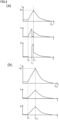
- FIG. 2 shows the time dependence of the current through the DC interrupting device in Embodiment 1 of the present invention.
- the vertical axes in FIG. 2 represent total current I, current I 1 , and current I 2 .
- the horizontal axes represent time t.
- the three graphs in FIG. 2(a) respectively show the time dependence of total current I, current I 1 , and current I 2 in the interruption operation of DC interrupting device 100 at the time of occurrence of fault current.
- a fault occurrence time T F indicates the same time in the graphs of total current I, current I 1 , and current I 2 .
- any point on each dashed line extending in parallel to the vertical axes indicate the same time.
- any point on the dashed line at the position of melting completion time T L1 in FIG. 2(a) indicates the same time in the three graphs of FIG. 2(a) .
- FIG. 2(b) shows the time dependence of the current of a DC interrupting device 101.
- DC interrupting device 101 is a device for comparison with DC interrupting device 100 in the description, and is not a DC interrupting device according to an Embodiment of the present invention.
- inductance values L 1 and L 2 are set to the same value.
- DC interrupting device 101 has the same configuration as DC interrupting device 100.
- the time when no fault current is generated is defined as "normal times".
- the time period before fault occurrence time T F at which a fault current occurs corresponds to "normal times”.
- total current I through DC interrupting device 100, current I 1 , and current I 2 are not time-dependent. Therefore, a voltage drop due to inductance components IC 1 and IC 2 does not occur.
- resistance values R 1 and R 2 are set to the same value, currents I 1 and I 2 are equal at normal times. Specifically, at normal times, currents I 1 and I 2 are half the total current I. Resistance values R 1 and R 2 can be equalized by, for example, adjusting the length and diameter of the cables.
- DC interrupting device 100 at normal times, total current I branches into current I 1 and current I 2 , so that the current through each of current-limiting fuses H 1 and H 2 is half the total current I. Accordingly, compared with a DC interrupting device where one current path has only one current-limiting fuse, DC interrupting device 100 can suppress the thermal deterioration of the fusible portions of fuse elements at normal times, and can also suppress the occurrence of erroneous melting of the fuse elements.
- Resistance values R 1 and R 2 are set to low enough relative to the impedance of current path 10 at the time of occurrence of fault current, and thus do not affect the branch ratio between current I 1 and current I 2 of immediately after the occurrence of fault current.
- the branch ratio between current path 10 and current path 20 at the time of occurrence of fault current is close to the ratio between inductance value L 1 and inductance value L 2 .
- Each current-limiting fuse has the properties as follows: each current-limiting fuse melts when an integration value exceeds a threshold value, where the integration value is obtained by integrating the value of current through the current-limiting fuse with respect to time for an integration interval, the integration interval being a time period during which the value of current through the current-limiting fuse exceeds the rated current. With such properties, current-limiting fuse H 1 melts in advance of current-limiting fuse H 2 .
- melting time T 1 the time at which current-limiting fuse H 1 melts is denoted by melting time T 1 .
- Current I 2 then increases, which causes current-limiting fuse H 2 to melt.
- melting completion time T L1 The time at which current-limiting fuse H 2 melts is denoted by melting completion time T L1 .
- Total current I at melting completion time T L1 is denoted by interruption current I p1 .
- Interruption current I p1 is the value of maximum current that flows through DC interrupting device 100 during the time period from the occurrence of fault to the completion of interruption.
- DC interrupting device 101 at the time of occurrence of fault current is described.
- the same names and reference sings are used as those of the elements of DC interrupting device 100. If a fault current occurs at fault occurrence time T F in FIG. 2(b) , total current I starts to increase immediately after fault occurrence time T F .
- DC interrupting device 101 where inductance values L 1 and L 2 are roughly equal, have roughly equal currents I 1 and I 2 at the time of occurrence of fault current. Therefore, current-limiting fuses H 1 and H 2 melt roughly at the same time.
- the melting time is denoted by melting completion time T L2 .
- Total current I through DC interrupting device 101 at melting completion time T L2 is denoted by interruption current I p2 .
- DC interrupting device 100 The characteristics of DC interrupting device 100 will now be described by comparing DC interrupting device 100 with DC interrupting device 101. Firstly, the time period between fault occurrence time T F and melting completion time T L2 is longer than the time period between fault occurrence time T F and melting completion time T L1 .
- the two current paths have different inductance values at the time of occurrence of fault. Accordingly, the current is not distributed but concentrated on each current path in succession. This can shorten the time period required for each current-limiting fuse to melt, thereby shortening the time period required for completing the melting of all the current-limiting fuses.
- DC interrupting device 100 which performs current-limiting in two steps, can make interruption current I p1 lower than interruption current I p2 .
- DC interrupting device 100 in Embodiment 1 can advantageously reduce the maximum value of fault current flowing at the time of current-limiting, as compared with DC interrupting device 101.
- DC interrupting device 100 can shorten the time period before the production of current zero in total current I through DC interrupting device 100 after the occurrence of fault, as compared with DC interrupting device 101. In other words, the time period between fault occurrence time T F and interruption time T I1 is shorter than the time period between fault occurrence time T F and interruption time T I2 .
- DC interrupting device 100 branches the current equally, which is achieved by the plurality of current paths having equal resistance components. Therefore, DC interrupting device 100 can suppress the progress of deterioration of the current-limiting fuses.
- DC interrupting device 100 in Embodiment 1 concentrates a current on each current path in succession for melting each current-limiting fuse.
- DC interrupting device 100 in Embodiment 1 can shorten the time period required for interruption or limitation of a fault current.
- DC interrupting device 100 can advantageously shorten the time period from fault occurrence time T F to melting completion time T L1 at which the current limiting on the fault current starts. Also, DC interrupting device 100 can reduce interruption current I p1 . This can advantageously reduce the damage to the devices connected to the fault site via the DC interrupting device, or can reduce the damage to the power grid.
- the DC interrupting device in Embodiment 1 of the present invention does not easily cause erroneous melting of the current-limiting fuses at normal times, and can also deliver good current-limiting performance at the time of occurrence of fault current.
- FIG. 1 While DC interrupting device 100 in FIG. 1 includes two current-limiting fuses connected in parallel, it may be modified into a DC interrupting device 100a that includes three or more current-limiting fuses connected in parallel, so as to more reliably suppress the deterioration of the fusible portions at normal times and deliver better current-limiting performance.
- FIG. 3 is a configuration diagram of a DC interrupting device including three or more current paths in Embodiment 1 of the present invention.
- DC interrupting device 100a includes current paths 10 to 10N.
- Current paths 10 to 10N are connected in parallel to one another at connection points C 1 and C 2 .
- DC interrupting device 100a includes first to Nth current paths connected at connection points C 1 and C 2 , this is not a limitation. The advantageous effects of the present invention can be obtained if the first to Nth current paths are connected in parallel and the relation of inductance components and the relation of resistance components among the current paths are defined as in DC interrupting device 100a.
- current path 10(k-1) and current path 10k are shown individually, among the plurality of current paths.
- current paths 10 to 10(k-2) are collectively shown as a parallel current path 250.
- k is not less than two and not more than N. In the following description, k denotes any number not less than two and not more than N.
- current paths 10(k+1) to 10N are collectively shown as a parallel current path 350.
- parallel current path 250 is not included.
- parallel current path 250 is constituted of only current path 10.
- parallel current path 350 is constituted of only current path 10N.
- parallel current path 350 is not included.
- Current path 10(k-1) has inductance component IC k-1 and resistance component RC k-1 .
- Current path 10k has inductance component IC k and resistance component RC k .
- resistance values R k and R k-1 are equal, and inductance value L k is higher than inductance value L k-1 .
- Current paths 10(k-1) and 10k respectively include current-limiting fuses H k-1 and H k .
- the current through the entire DC interrupting device 100a is denoted by total current I a .
- the current through current path 10(k-1) is denoted by current I k-1, a .
- the current through current path 10k is denoted by current I k, a .
- DC interrupting device 100a at the time of occurrence of fault current.
- the current can flow only through current path 10(k-1), current path 10k, and parallel current path 350, except for currents caused by electric arcs.
- inductance value L k is higher than inductance value L k-1 . More preferably, the inductance value of the inductance component of the current path constituted of current path 10k and parallel current path 350 is higher than inductance value L k-1 . With such a configuration, the fault current concentrates on current path 10(k-1) and thus can melt current-limiting fuse H k-1 in a short time period.
- the fault current concentrates on current path 10k and melts current-limiting fuse H k .
- the fault current concentrates on each of the first to Nth current paths in succession and melts each current-limiting fuse, thus allowing completion of current limiting in a short time period.
- DC interrupting device 100a in Embodiment 1 which has three or more current-limiting fuses and current paths, can reduce the value of current flowing through each current-limiting fuse at normal times, as compared with the case of two current paths. Therefore, erroneous melting is less likely to occur than in the case of two current paths.
- the fusible portions are smaller in wire diameter than those in the case of two current paths, better current-limiting performance can be delivered, while the likelihood of erroneous melting is maintained at the same level as with two current paths.
- the inductance value of current path 10(k-1) is set to lower than the inductance value of the parallel circuit constituted of current paths 10k to 10N. This allows the current to concentrate on each current path at staggered times, thereby shortening the time period required for each current-limiting fuse to melt.
- DC interrupting device 100 including two or more current-limiting fuses is configured as follows.
- DC interrupting device 100 includes a (k-1)th current path including a (k-1)th current-limiting fuse, where k is an integer of not less than two and not more than N, and N is an integer of not less than two.
- DC interrupting device 100 further includes a kth current path connected in parallel to the (k-1)th current path and including a kth current-limiting fuse. The inductance value of the inductance component of the kth current path is higher than the inductance value of the inductance component of the (k-1)th current path.
- the first to Nth current paths are equal in resistance component.
- the current paths equal in resistance component, allow an equal current to flow through the current paths at normal times. Accordingly, the value of current through each current path can be minimized. This can reduce the deterioration of the current-limiting fuses at normal times and also reduce the occurrence of erroneous melting of the current-limiting fuses.
- the inductance value of the inductance component of the parallel current path constituted of the kth to Nth current paths may be twice or more as high as the inductance value of the inductance component of the (k-1)th current path, where k is an integer of not less than two and not more than N, and N is an integer of not less than two. In this case, the following advantageous effects are provided.
- the impedance value of the (k-1)th current path is half or less the impedance value of the parallel current path constituted of the kth to Nth current paths. Therefore, the current concentrates on the kth current path, thereby shortening the time required for completing the melting of all the current paths.
- the DC interrupting device in the present Embodiment includes a plurality of current paths, among which a current is distributed at normal times.
- the current paths which have different inductance components, produce different impedances at the time of occurrence of fault current.
- the current concentrates on each current path in succession, in ascending order according to its inductance component.
- the interruption current can be suppressed.
- the interruption current is the maximum value of current flowing through the DC interrupting device during the time period from the occurrence of fault to the completion of interruption. Further, the time period can be shortened from the occurrence of fault current to the completion of the current interruption.
- DC interrupting device in the present Embodiment can advantageously reduce the occurrence of erroneous melting of the current-limiting fuses at normal times with no fault current, and can also deliver good current-limiting performance at the time of occurrence of fault current.
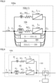
- a DC interrupting device 100b in Embodiment 2 includes a circuit breaker 3 in addition to and connected in series to DC interrupting device 100 in Embodiment 1.
- FIG. 4 shows a configuration of a DC interrupting device in Embodiment 2 of the present invention.
- the layouts and ranges of current paths 10 and 20 are the same as those of FIG. 1 .
- a parallel current path constituted of current paths 10 and 20 is denoted by a parallel current path 150.
- DC interrupting device 100b additionally includes circuit breaker 3.
- DC interrupting device 100b is obtained by connecting circuit breaker 3 in series to DC interrupting device 100 that has two current paths.
- circuit breaker 3 may be connected in series to DC interrupting device 100a that has three or more current paths.
- Such a DC interrupting device can also provide the advantageous effects of the present invention as with DC interrupting device 100b.
- an overcurrent detection device 4 detects the fault current and inputs a circuit-breaker opening signal to circuit breaker 3. Upon receiving the circuit-breaker opening signal, circuit breaker 3 opens its contacts.
- a chopping current value differs depending on the circuit breaker.
- circuit breaker 3 is connected in series to parallel current path 150.
- DC interrupting device 100b can interrupt the direct current using circuit breaker 3 after limiting the current by melting the current-limiting fuses. In this way, DC interrupting device 100b can interrupt a fault current in an electrical circuit with a high-voltage that would be difficult to interrupt using current-limiting fuses alone.
- DC interrupting device 100b that can interrupt a fault current is designed as follows, for example. First, a fault current that can occur in the power grid provided with DC interrupting device 100b is estimated with respect to its current value, current waveform and the like, including the safety factor. Then, based on the estimated fault current, the current value after the current limiting via current-limiting fuses H 1 and H 2 is predicted.
- circuit breaker 3 and current-limiting fuses H 1 and H 2 are designed or selected from among commercially available products so that the predicted current value after the current limiting will be equal to or lower than the chopping current value.
- DC interrupting device 100b that can interrupt a fault current can be designed, including the safety factor.
- circuit breaker 3 Examples of the types of electric arcs which cause the current chopping phenomenon include gas arcs and vacuum arcs.
- the insulating medium or extinguishing medium of circuit breaker 3 can be selected in accordance with the properties desired for the circuit breaker.
- a gas can be selected as the insulating medium or extinguishing medium.
- circuit breaker 3 may be a vacuum circuit breaker.
- DC interrupting device 100b in Embodiment 2 does not easily cause erroneous melting of the current-limiting fuses at normal times with no fault current, and can also deliver good current-limiting performance at the time of occurrence of fault current.
- circuit breaker 3 is connected in series to parallel current path 150.
- DC interrupting device 100b can interrupt the current using circuit breaker 3 after limiting the current by melting the current-limiting fuses.
- the DC interrupting device 100b can interrupt a fault current generating a voltage of several kV or more between the terminals that would be difficult to interrupt using current-limiting fuses alone.
- a DC interrupting device 100c in Embodiment 3 further includes a lightning arrester 5 connected in parallel to parallel current path 150, in addition to DC interrupting device 100b described in Embodiment 2.
- FIG. 5 shows a configuration of a DC interrupting device in Embodiment 3 of the present invention.
- the same parts as those of DC interrupting device 100b shown in FIG. 4 in Embodiment 2 are denoted by the same reference signs, and the detailed description thereof is not repeated.
- Lightning arrester 5 is connected in parallel to parallel current path 150 at connection points C 1 and C 2 .
- the current path including lightning arrester 5 and connecting between connection points C 1 and C 2 is referred to as a current path 30.
- the current through the entire DC interrupting device 100c is denoted by total current I c .
- the current through current path 10 is denoted by current I 1c
- the current through current path 20 is denoted by current I 2c
- the current through current path 30 is denoted by current I 3 .
- lightning arrester 5 is connected in parallel to parallel current path 150 at connection points C 1 and C 2 in Embodiment 3, this is not a limitation of the present invention.
- the advantageous effects of the present invention can be obtained if lightning arrester 5 is connected in parallel to parallel current path 150.
- any other configuration may be employed to obtain the same advantageous effects, as long as the voltage between the terminals of current-limiting fuse H 1 or H 2 is applied across lightning arrester 5.
- current-limiting fuses H 1 and H 2 melt in succession to limit the current, and then circuit breaker 3 interrupts the current.
- a current-limiting fuse having a higher voltage between its terminals when melted can shorten the time period before the start of current limiting after the occurrence of fault current, and thus can shorten the time period before the production of current zero after the occurrence of fault current.
- a current-limiting fuse having a higher voltage between its terminals delivers better current-limiting performance.
- the voltage between the terminals of current-limiting fuse H 1 or H 2 may exceed the voltage limit of the power grid. This may damage component devices of the power grid.
- the component devices of the power grid include an AC-DC converter (a device that converts between AC and DC) and a DC-DC converter (a device that converts DC voltages).
- DC interrupting device 100c does not easily cause erroneous melting of the current-limiting fuses at normal times with no fault current, and can also deliver good current-limiting performance at the time of occurrence of fault current.
- circuit breaker 3 is connected in series to parallel current path 150.
- DC interrupting device 100c can interrupt the direct current by the voltage between the terminals of circuit breaker 3, after limiting the current by melting the current-limiting fuses included in parallel current path 150. In this way, DC interrupting device 100c can interrupt a direct current with a several kV or more that would be difficult to interrupt using high voltage fuses alone.
- DC interrupting device 100c which includes lightning arrester 5, allows a current to flow through lightning arrester 5 when the voltage between the terminals of current-limiting fuse H 1 or H 2 exceeds the discharge starting voltage. Thus, the voltage between the terminals of current-limiting fuse H 1 or H 2 can be reduced.
- lightning arrester 5 can reduce the voltage between the terminals of current-limiting fuse H 1 or H 2 to equal to or lower than the discharge starting voltage, thus advantageously preventing damage to the devices included in the power grid.
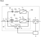
- a DC interrupting device in Embodiment 4 includes a switch 6 in addition to the construction described in Embodiment 2.
- FIG. 6 shows a configuration of a DC interrupting device in Embodiment 4 of the present invention.
- the same parts as those of DC interrupting device 100b shown in FIG. 4 in Embodiment 2 are denoted by the same reference signs, and the detailed description thereof is not repeated.
- DC interrupting device 100d in Embodiment 4 has the construction described in Embodiment 2. Further, switch 6 is connected in parallel to parallel current path 150 at connection points C 1 and C 2 .
- the current path including switch 6 and connecting between connection points C 1 and C 2 is referred to as a current path 40.
- the current through current path 40 is denoted by I 4 .
- DC interrupting device 100d includes circuit breaker 3, the advantageous effects of the present invention can be obtained without circuit breaker 3. The advantageous effects of the present invention can also be obtained if DC interrupting device 100d additionally includes lightning arrester 5 connected in parallel to parallel current path 150, as in DC interrupting device 100c.
- the current through DC interrupting device 100d is denoted by total current I d .
- the current through current path 10 is denoted by I 1d
- the current through current path 20 is denoted by I 2d .
- FIG. 7 shows the time dependence of the current through the DC interrupting device in Embodiment 4 of the present invention.
- FIG. 7 shows temporal waveforms of the currents through current paths 10, 20, and 40 when a fault current occurs.
- T F denotes the fault occurrence time at which a fault current occurs in the power grid.
- T S denotes the contact-opening starting time at which the switch starts opening its contacts.
- T 4 denotes the contact-disconnection time, i.e., the instant at which the contacts of switch 6 are physically disconnected.
- T 1 denotes the melting time at which current-limiting fuse H 1 melts.
- T L denotes the melting completion time at which current-limiting fuse H 2 melts.
- I p denotes the interruption current, which is the current at melting completion time T L .
- the three horizontal axes share the same time.
- fault occurrence time T F indicates the same time in the graphs of total current I d , current I 1d , and current I 2d .
- any point on each dashed line extending in parallel to the vertical axes indicate the same time.
- Switch 6 includes a pair of contacts connectable and disconnectable and configured to open in response to a contact-opening instruction signal 2.
- a contact-opening instruction signal outputted to circuit breaker 3 is denoted by contact-opening instruction signal 1
- a contact-opening instruction signal outputted to switch 6 is denoted by contact-opening instruction signal 2.
- Contact-opening instruction signals 1 and 2 may be simultaneously generated, or may be staggered after the detection of a fault current.
- Overcurrent detection device 4 detects the fault current and outputs contact-opening instruction signal 2 to switch 6. Upon receiving contact-opening instruction signal 2, switch 6 starts disconnecting the pair of contacts at contact-opening starting time T S .
- inductance value L 2 is set to higher than inductance value L 1
- the electrical resistance of current path 40 is set to higher than resistance value R 1 .
- current I 4 at contact-disconnection time T 4 is set to equal to or lower than the chopping current value, which is the maximum current value that allows switch 6 to be chopped.
- Current I 4 at contact-disconnection time T 4 can be adjusted to equal to or lower than the chopping current value by adjusting the magnitude relation between the resistance between the contacts of switch 6 and resistance component RC 1 of current path 10.
- the chopping current value differs depending on the switch.
- Current I 4 at contact-disconnection time T 4 can be adjusted to equal to or lower than the chopping current value by calculation or test, in consideration of the specifications of the switch, the properties of a fault current that can be generated in the power grid, and the like.
- DC interrupting device 100d can not only suppress the progress of thermal deterioration of the fuse elements at normal times, but also interrupt the current quickly.
- the deteriorated insulation performance between the contacts refers to a state in which an electric arc is likely to occur, that is, a state in which an electric arc can occur between the contacts even with a low voltage between the contacts.
- the voltage generated in parallel current path 150 refers to a voltage generated across current-limiting fuse H 1 at melting time T 1 , or a voltage generated across current-limiting fuses H 1 and H 2 at melting completion time T L .
- the electrical resistance between the terminals of switch 6 is set to much higher than resistance value R 1 , and current I 4 at contact-disconnection time T 4 is set to equal to or lower than the maximum chopping current value. Therefore, the recurrence of electric arc between the contacts of switch 6 can be suppressed.
- DC interrupting device 100d does not easily cause erroneous melting of the current-limiting fuses at normal times with no fault current, and can also deliver good current-limiting performance at the time of occurrence of fault current.
- circuit breaker 3 is connected in series to parallel current path 150.
- DC interrupting device 100d can interrupt the direct current by the potential difference between the terminals of circuit breaker 3, after limiting the current by melting the current-limiting fuses included in parallel current path 150. In this way, DC interrupting device 100d can interrupt a direct current with a several kV or more that would be difficult to interrupt using high voltage fuses alone.
- DC interrupting device 100d in Embodiment 4 which includes switch 6 connected in parallel to parallel current path 150, can further suppress the current through the current-limiting fuses at normal times, thereby further suppressing the deterioration of the current-limiting fuses.
- current I 4 at contact-disconnection time T 4 is set to lower than the chopping current value of switch 6 by adjusting the magnitude relation between the resistance between the terminals of switch 6 and resistance value R 1 . This can suppress the occurrence of an electric arc between the contacts of switch 6 at the time of commutation to parallel current path 150, thereby suppressing the recurrence of electric arc between the contacts of switch 6 after the current limiting by parallel current path 150 is completed.
Landscapes
- Engineering & Computer Science (AREA)
- Power Engineering (AREA)
- Emergency Protection Circuit Devices (AREA)
- Driving Mechanisms And Operating Circuits Of Arc-Extinguishing High-Tension Switches (AREA)
- Fuses (AREA)
Claims (8)
- Gleichstrom unterbrechende Vorrichtung, umfassend:einen (k-1)-ten Strompfad (10(k-1)), der eine (k-1)te Strombegrenzungssicherung (Hk-1) enthält, wobei k eine ganze Zahl von nicht weniger als zwei und nicht mehr als N ist, und N eine ganze Zahl von nicht weniger als zwei ist; undeinen k-ten Strompfad (10k), der parallel an den (k-1)-ten Strompfad (10(k-1)) angeschlossen ist und eine k-te Strombegrenzungssicherung (Hk) enthält, wobei ein Induktivitätswert einer Induktivitätskomponente des k-ten Strompfads (10k) höher ist als ein Induktivitätswert einer Induktivitätskomponente des (k-1)-ten Strompfads (10(k-1));wobei der erste bis N-te Strompfad (10 - 10N) Widerstandskomponenten haben, die gleich im Widerstandswert sind.
- Gleichstrom unterbrechende Vorrichtung nach Anspruch 1, umfassend:einen ersten Strompfad (10), der eine erste Strombegrenzungssicherung (H1) enthält; undeinen zweiten Strompfad (20), der parallel an die erste Strombegrenzungssicherung (H1) angeschlossen ist und eine zweite Strombegrenzungssicherung (H2) enthält, wobei ein Induktivitätswert einer Induktivitätskomponente des zweiten Strompfads (20) höher ist als ein Induktivitätswert einer Induktivitätskomponente des ersten Strompfads (10).
- Gleichstrom unterbrechende Vorrichtung nach einem der Ansprüche 1 bis 2, wobei ein Induktivitätswert einer Induktivitätskomponente eines parallelen Strompfads, der aus den k-ten bis N-ten Strompfaden (10k - 10N) besteht, höher ist als der Induktivitätswert der Induktivitätskomponente des (k-1)-ten Strompfads (10(k-1)).
- Gleichstrom unterbrechende Vorrichtung nach einem der Ansprüche 1 bis 3, wobei ein Induktivitätswert einer Induktivitätskomponente eines parallelen Strompfads, der aus den k-ten bis N-ten Strompfaden (10k - 10N) besteht, zweimal oder mehr so hoch wie der Induktivitätswert der Induktivitätskomponente des (k-1)-ten Strompfads (10(k-1)) ist.
- Gleichstrom unterbrechende Vorrichtung nach einem der Ansprüche 1 bis 4, darüber hinaus einen Leistungsschalter (3) umfassend, der in Reihe an einen parallelen Strompfad (150) angeschlossen ist, der aus den ersten bis N-ten Strompfaden (10 - 10N) besteht, wobei der Leistungsschalter ein Paar von anschließbaren und nicht anschließbaren Kontakten enthält.
- Gleichstrom unterbrechende Vorrichtung nach einem der Ansprüche 1 bis 5, darüber hinaus einen Blitzableiter (5) umfassend, der parallel an einen parallelen Strompfad (150) angeschlossen ist, der aus den ersten bis N-ten Strompfaden (10 - 10N) besteht.
- Gleichstrom unterbrechende Vorrichtung nach Anspruch 6, wobei,wenn eine am parallelen Strompfad (150) anliegende Spannung unter einer Entladebeginnspannung liegt, der Blitzableiter (5) isoliert gehalten wird, undwenn die am parallelen Strompfad (150) anliegende Spannung über der Endladebeginnspannung liegt, ein Strom durch den Blitzableiter (5) fließt, so dass die am parallelen Strompfad (150) anliegende Spannung auf gleich oder niedriger als die Entladebeginnspannung reduziert wird.
- Gleichstrom unterbrechende Vorrichtung nach einem der Ansprüche 1 bis 7, darüber hinaus einen Schalter (6) umfassend, der parallel an einen parallelen Strompfad (150) angeschlossen ist, der aus den ersten bis N-ten Strompfaden (10 - 10N) besteht, wobeider Schalter (6) ein Paar Kontakte enthält,wobeiein Zerhackungsstromwert des Schalters (6) höher ist als ein Strom, der durch den Schalter (6) in einem Augenblick fließt, wenn die Kontakte des Schalters (6) getrennt sind.
Applications Claiming Priority (1)
| Application Number | Priority Date | Filing Date | Title |
|---|---|---|---|
| PCT/JP2017/040461 WO2019092834A1 (ja) | 2017-11-09 | 2017-11-09 | 直流遮断装置 |
Publications (4)
| Publication Number | Publication Date |
|---|---|
| EP3709326A1 EP3709326A1 (de) | 2020-09-16 |
| EP3709326A4 EP3709326A4 (de) | 2020-11-18 |
| EP3709326B1 true EP3709326B1 (de) | 2024-01-24 |
| EP3709326B9 EP3709326B9 (de) | 2024-04-03 |
Family
ID=66438346
Family Applications (1)
| Application Number | Title | Priority Date | Filing Date |
|---|---|---|---|
| EP17931794.6A Active EP3709326B9 (de) | 2017-11-09 | 2017-11-09 | Gleichstromunterbrechungsvorrichtung |
Country Status (4)
| Country | Link |
|---|---|
| US (1) | US11233391B2 (de) |
| EP (1) | EP3709326B9 (de) |
| JP (1) | JP7018959B2 (de) |
| WO (1) | WO2019092834A1 (de) |
Families Citing this family (2)
| Publication number | Priority date | Publication date | Assignee | Title |
|---|---|---|---|---|
| EP4340149A4 (de) * | 2021-06-28 | 2024-08-28 | Huawei Digital Power Technologies Co., Ltd. | Schutzschalter und stromversorgungssystem |
| FR3126075B1 (fr) * | 2021-08-09 | 2023-08-04 | Inst Supergrid | Dispositif et Procédé de coupure de courant électrique sous haute tension continue avec fusible et système de surcharge à courant oscillant |
Family Cites Families (17)
| Publication number | Priority date | Publication date | Assignee | Title |
|---|---|---|---|---|
| JPS57119420A (en) | 1981-01-16 | 1982-07-24 | Toshiaki Arai | Method of controlling operating overvoltage for current limiting fuse |
| JPS6282538U (de) | 1985-11-12 | 1987-05-26 | ||
| JPH05236646A (ja) * | 1992-02-21 | 1993-09-10 | Mitsubishi Electric Corp | 限流装置 |
| US6075684A (en) * | 1998-03-23 | 2000-06-13 | Electric Boat Corporation | Method and arrangement for direct current circuit interruption |
| JPH11273905A (ja) * | 1998-03-25 | 1999-10-08 | Ngk Insulators Ltd | 複数のptc素子板を並列接続して構成した限流器 |
| US6583977B1 (en) * | 1999-10-27 | 2003-06-24 | Motorola, Inc. | Zipper fuse |
| JP2007028584A (ja) | 2005-06-16 | 2007-02-01 | Mitsubishi Materials Corp | 電力線通信システム及び電力線通信方法 |
| JP4635989B2 (ja) | 2006-09-01 | 2011-02-23 | 富士電機システムズ株式会社 | 電流遮断装置 |
| ES2428001T3 (es) * | 2008-11-26 | 2013-11-05 | Abb Technology Ag | Disposición de disyuntor para corriente continua de alto voltaje y método asociado |
| FR2985082B1 (fr) * | 2011-12-23 | 2014-02-21 | Alstom Technology Ltd | Dispositif disjoncteur mecatronique et procede de declenchement associe et application a la coupure de courant continu eleve |
| EP2846342B1 (de) * | 2012-05-01 | 2019-02-06 | Mitsubishi Electric Corporation | Dc-schutzschalter |
| JP5948176B2 (ja) * | 2012-07-24 | 2016-07-06 | 株式会社日立製作所 | 開閉器 |
| EP2698892B1 (de) * | 2012-08-13 | 2018-07-11 | DET International Holding Limited | DC Überstromschutzvorrichtung |
| EP2888749B1 (de) * | 2012-08-27 | 2016-06-22 | ABB Technology Ltd. | Gerät eingerichtet zur unterbrechung des elektrischen stroms |
| US8867180B2 (en) * | 2012-11-30 | 2014-10-21 | Tesla Motors, Inc. | Dynamic current protection in energy distribution systems |
| KR101658539B1 (ko) | 2014-10-10 | 2016-09-22 | 엘에스산전 주식회사 | 직류 차단기 및 이를 이용하는 방법 |
| JP2016163202A (ja) * | 2015-03-03 | 2016-09-05 | 三菱電機株式会社 | 半導体遮断器 |
-
2017
- 2017-11-09 JP JP2019551825A patent/JP7018959B2/ja active Active
- 2017-11-09 US US16/753,401 patent/US11233391B2/en active Active
- 2017-11-09 WO PCT/JP2017/040461 patent/WO2019092834A1/ja not_active Ceased
- 2017-11-09 EP EP17931794.6A patent/EP3709326B9/de active Active
Also Published As
| Publication number | Publication date |
|---|---|
| US11233391B2 (en) | 2022-01-25 |
| JPWO2019092834A1 (ja) | 2020-11-12 |
| EP3709326B9 (de) | 2024-04-03 |
| US20200287380A1 (en) | 2020-09-10 |
| EP3709326A4 (de) | 2020-11-18 |
| JP7018959B2 (ja) | 2022-02-14 |
| EP3709326A1 (de) | 2020-09-16 |
| WO2019092834A1 (ja) | 2019-05-16 |
Similar Documents
| Publication | Publication Date | Title |
|---|---|---|
| US9337640B2 (en) | Electrical protection device and method | |
| CN104488156B (zh) | 故障排除的方法 | |
| US9054557B2 (en) | Voltage balancing of symmetric HVDC monopole transmission lines after earth faults | |
| US20200106258A1 (en) | Dc circuit breaker with an alternating commutating circuit | |
| EP3306766B2 (de) | Gleichstromübertragungssystem, zentraler server dieses systems und verfahren zur wiederherstellung eines gleichstromübertragungswegs nach einem ausfall | |
| US9478974B2 (en) | DC voltage circuit breaker | |
| CN107005045B (zh) | 高压直流电流断路装置 | |
| CN107533926B (zh) | 旁路开关、提供导电路径的方法和功率系统 | |
| CN106129954B (zh) | 断路器 | |
| CN105659465A (zh) | Hvdc的ac侧电气保护 | |
| EP3709326B1 (de) | Gleichstromunterbrechungsvorrichtung | |
| JP2011010483A (ja) | 電流分離器及び電流遮断装置 | |
| US10333313B2 (en) | Electrical assembly | |
| CN110581539B (zh) | 一种用于直流配电网的保护装置及其保护方法 | |
| CN108369876A (zh) | 带有强制电流振荡的用于高压dc网络的断路器 | |
| KR101802509B1 (ko) | 캐스케이드 하프 브리지 sscb | |
| WO2016209164A1 (en) | Power system and method of forming the same | |
| Ouaida et al. | DC GRIDS: New over current protection | |
| Rezaei et al. | Ultra fast protection of radial and looped electric power grid using a novel solid-state protection device | |
| Li et al. | Study on the Matching of Solid State Power Controller in Cascade Application | |
| Howe et al. | DC fusing in semiconductor circuits | |
| CN110277764B (zh) | 一种电网过压保护电路和方法 | |
| Varodi et al. | Diagnosis of short circuit and the earthing of a transformer station | |
| Reymond-Laruina et al. | The use of ultra-fast LVAC fuses in DC grids: state of art, testing and recommendations | |
| Ouaida et al. | New over current protection technology addressing DC Transportation |
Legal Events
| Date | Code | Title | Description |
|---|---|---|---|
| STAA | Information on the status of an ep patent application or granted ep patent |
Free format text: STATUS: THE INTERNATIONAL PUBLICATION HAS BEEN MADE |
|
| PUAI | Public reference made under article 153(3) epc to a published international application that has entered the european phase |
Free format text: ORIGINAL CODE: 0009012 |
|
| STAA | Information on the status of an ep patent application or granted ep patent |
Free format text: STATUS: REQUEST FOR EXAMINATION WAS MADE |
|
| 17P | Request for examination filed |
Effective date: 20200504 |
|
| AK | Designated contracting states |
Kind code of ref document: A1 Designated state(s): AL AT BE BG CH CY CZ DE DK EE ES FI FR GB GR HR HU IE IS IT LI LT LU LV MC MK MT NL NO PL PT RO RS SE SI SK SM TR |
|
| AX | Request for extension of the european patent |
Extension state: BA ME |
|
| REG | Reference to a national code |
Ref country code: DE Ref legal event code: R079 Free format text: PREVIOUS MAIN CLASS: H01H0009540000 Ipc: H02H0003087000 Ref country code: DE Ref legal event code: R079 Ref document number: 602017078824 Country of ref document: DE Free format text: PREVIOUS MAIN CLASS: H01H0009540000 Ipc: H02H0003087000 |
|
| A4 | Supplementary search report drawn up and despatched |
Effective date: 20201019 |
|
| RIC1 | Information provided on ipc code assigned before grant |
Ipc: H02H 3/087 20060101AFI20201013BHEP Ipc: H01H 33/59 20060101ALI20201013BHEP Ipc: H01H 9/54 20060101ALI20201013BHEP |
|
| DAV | Request for validation of the european patent (deleted) | ||
| DAX | Request for extension of the european patent (deleted) | ||
| STAA | Information on the status of an ep patent application or granted ep patent |
Free format text: STATUS: EXAMINATION IS IN PROGRESS |
|
| 17Q | First examination report despatched |
Effective date: 20220302 |
|
| GRAP | Despatch of communication of intention to grant a patent |
Free format text: ORIGINAL CODE: EPIDOSNIGR1 |
|
| STAA | Information on the status of an ep patent application or granted ep patent |
Free format text: STATUS: GRANT OF PATENT IS INTENDED |
|
| INTG | Intention to grant announced |
Effective date: 20230821 |
|
| P01 | Opt-out of the competence of the unified patent court (upc) registered |
Effective date: 20231006 |
|
| GRAS | Grant fee paid |
Free format text: ORIGINAL CODE: EPIDOSNIGR3 |
|
| GRAA | (expected) grant |
Free format text: ORIGINAL CODE: 0009210 |
|
| STAA | Information on the status of an ep patent application or granted ep patent |
Free format text: STATUS: THE PATENT HAS BEEN GRANTED |
|
| AK | Designated contracting states |
Kind code of ref document: B1 Designated state(s): AL AT BE BG CH CY CZ DE DK EE ES FI FR GB GR HR HU IE IS IT LI LT LU LV MC MK MT NL NO PL PT RO RS SE SI SK SM TR |
|
| REG | Reference to a national code |
Ref country code: GB Ref legal event code: FG4D |
|
| REG | Reference to a national code |
Ref country code: CH Ref legal event code: EP |
|
| REG | Reference to a national code |
Ref country code: DE Ref legal event code: R096 Ref document number: 602017078824 Country of ref document: DE |
|
| REG | Reference to a national code |
Ref country code: IE Ref legal event code: FG4D |
|
| REG | Reference to a national code |
Ref country code: CH Ref legal event code: PK Free format text: BERICHTIGUNG B9 |
|
| REG | Reference to a national code |
Ref country code: LT Ref legal event code: MG9D |
|
| REG | Reference to a national code |
Ref country code: NL Ref legal event code: MP Effective date: 20240124 |
|
| PG25 | Lapsed in a contracting state [announced via postgrant information from national office to epo] |
Ref country code: NL Free format text: LAPSE BECAUSE OF FAILURE TO SUBMIT A TRANSLATION OF THE DESCRIPTION OR TO PAY THE FEE WITHIN THE PRESCRIBED TIME-LIMIT Effective date: 20240124 |
|
| PG25 | Lapsed in a contracting state [announced via postgrant information from national office to epo] |
Ref country code: NL Free format text: LAPSE BECAUSE OF FAILURE TO SUBMIT A TRANSLATION OF THE DESCRIPTION OR TO PAY THE FEE WITHIN THE PRESCRIBED TIME-LIMIT Effective date: 20240124 |
|
| PG25 | Lapsed in a contracting state [announced via postgrant information from national office to epo] |
Ref country code: IS Free format text: LAPSE BECAUSE OF FAILURE TO SUBMIT A TRANSLATION OF THE DESCRIPTION OR TO PAY THE FEE WITHIN THE PRESCRIBED TIME-LIMIT Effective date: 20240524 |
|
| PG25 | Lapsed in a contracting state [announced via postgrant information from national office to epo] |
Ref country code: LT Free format text: LAPSE BECAUSE OF FAILURE TO SUBMIT A TRANSLATION OF THE DESCRIPTION OR TO PAY THE FEE WITHIN THE PRESCRIBED TIME-LIMIT Effective date: 20240124 |
|
| PG25 | Lapsed in a contracting state [announced via postgrant information from national office to epo] |
Ref country code: GR Free format text: LAPSE BECAUSE OF FAILURE TO SUBMIT A TRANSLATION OF THE DESCRIPTION OR TO PAY THE FEE WITHIN THE PRESCRIBED TIME-LIMIT Effective date: 20240425 |
|
| REG | Reference to a national code |
Ref country code: AT Ref legal event code: MK05 Ref document number: 1652932 Country of ref document: AT Kind code of ref document: T Effective date: 20240124 |
|
| PG25 | Lapsed in a contracting state [announced via postgrant information from national office to epo] |
Ref country code: HR Free format text: LAPSE BECAUSE OF FAILURE TO SUBMIT A TRANSLATION OF THE DESCRIPTION OR TO PAY THE FEE WITHIN THE PRESCRIBED TIME-LIMIT Effective date: 20240124 Ref country code: RS Free format text: LAPSE BECAUSE OF FAILURE TO SUBMIT A TRANSLATION OF THE DESCRIPTION OR TO PAY THE FEE WITHIN THE PRESCRIBED TIME-LIMIT Effective date: 20240424 |
|
| PG25 | Lapsed in a contracting state [announced via postgrant information from national office to epo] |
Ref country code: ES Free format text: LAPSE BECAUSE OF FAILURE TO SUBMIT A TRANSLATION OF THE DESCRIPTION OR TO PAY THE FEE WITHIN THE PRESCRIBED TIME-LIMIT Effective date: 20240124 |
|
| PG25 | Lapsed in a contracting state [announced via postgrant information from national office to epo] |
Ref country code: AT Free format text: LAPSE BECAUSE OF FAILURE TO SUBMIT A TRANSLATION OF THE DESCRIPTION OR TO PAY THE FEE WITHIN THE PRESCRIBED TIME-LIMIT Effective date: 20240124 |
|
| PG25 | Lapsed in a contracting state [announced via postgrant information from national office to epo] |
Ref country code: RS Free format text: LAPSE BECAUSE OF FAILURE TO SUBMIT A TRANSLATION OF THE DESCRIPTION OR TO PAY THE FEE WITHIN THE PRESCRIBED TIME-LIMIT Effective date: 20240424 Ref country code: NO Free format text: LAPSE BECAUSE OF FAILURE TO SUBMIT A TRANSLATION OF THE DESCRIPTION OR TO PAY THE FEE WITHIN THE PRESCRIBED TIME-LIMIT Effective date: 20240424 Ref country code: LT Free format text: LAPSE BECAUSE OF FAILURE TO SUBMIT A TRANSLATION OF THE DESCRIPTION OR TO PAY THE FEE WITHIN THE PRESCRIBED TIME-LIMIT Effective date: 20240124 Ref country code: IS Free format text: LAPSE BECAUSE OF FAILURE TO SUBMIT A TRANSLATION OF THE DESCRIPTION OR TO PAY THE FEE WITHIN THE PRESCRIBED TIME-LIMIT Effective date: 20240524 Ref country code: HR Free format text: LAPSE BECAUSE OF FAILURE TO SUBMIT A TRANSLATION OF THE DESCRIPTION OR TO PAY THE FEE WITHIN THE PRESCRIBED TIME-LIMIT Effective date: 20240124 Ref country code: GR Free format text: LAPSE BECAUSE OF FAILURE TO SUBMIT A TRANSLATION OF THE DESCRIPTION OR TO PAY THE FEE WITHIN THE PRESCRIBED TIME-LIMIT Effective date: 20240425 Ref country code: FI Free format text: LAPSE BECAUSE OF FAILURE TO SUBMIT A TRANSLATION OF THE DESCRIPTION OR TO PAY THE FEE WITHIN THE PRESCRIBED TIME-LIMIT Effective date: 20240124 Ref country code: ES Free format text: LAPSE BECAUSE OF FAILURE TO SUBMIT A TRANSLATION OF THE DESCRIPTION OR TO PAY THE FEE WITHIN THE PRESCRIBED TIME-LIMIT Effective date: 20240124 Ref country code: BG Free format text: LAPSE BECAUSE OF FAILURE TO SUBMIT A TRANSLATION OF THE DESCRIPTION OR TO PAY THE FEE WITHIN THE PRESCRIBED TIME-LIMIT Effective date: 20240124 Ref country code: AT Free format text: LAPSE BECAUSE OF FAILURE TO SUBMIT A TRANSLATION OF THE DESCRIPTION OR TO PAY THE FEE WITHIN THE PRESCRIBED TIME-LIMIT Effective date: 20240124 |
|
| PG25 | Lapsed in a contracting state [announced via postgrant information from national office to epo] |
Ref country code: PT Free format text: LAPSE BECAUSE OF FAILURE TO SUBMIT A TRANSLATION OF THE DESCRIPTION OR TO PAY THE FEE WITHIN THE PRESCRIBED TIME-LIMIT Effective date: 20240524 Ref country code: PL Free format text: LAPSE BECAUSE OF FAILURE TO SUBMIT A TRANSLATION OF THE DESCRIPTION OR TO PAY THE FEE WITHIN THE PRESCRIBED TIME-LIMIT Effective date: 20240124 |
|
| PG25 | Lapsed in a contracting state [announced via postgrant information from national office to epo] |
Ref country code: SE Free format text: LAPSE BECAUSE OF FAILURE TO SUBMIT A TRANSLATION OF THE DESCRIPTION OR TO PAY THE FEE WITHIN THE PRESCRIBED TIME-LIMIT Effective date: 20240124 Ref country code: PT Free format text: LAPSE BECAUSE OF FAILURE TO SUBMIT A TRANSLATION OF THE DESCRIPTION OR TO PAY THE FEE WITHIN THE PRESCRIBED TIME-LIMIT Effective date: 20240524 Ref country code: PL Free format text: LAPSE BECAUSE OF FAILURE TO SUBMIT A TRANSLATION OF THE DESCRIPTION OR TO PAY THE FEE WITHIN THE PRESCRIBED TIME-LIMIT Effective date: 20240124 Ref country code: LV Free format text: LAPSE BECAUSE OF FAILURE TO SUBMIT A TRANSLATION OF THE DESCRIPTION OR TO PAY THE FEE WITHIN THE PRESCRIBED TIME-LIMIT Effective date: 20240124 |
|
| PG25 | Lapsed in a contracting state [announced via postgrant information from national office to epo] |
Ref country code: DK Free format text: LAPSE BECAUSE OF FAILURE TO SUBMIT A TRANSLATION OF THE DESCRIPTION OR TO PAY THE FEE WITHIN THE PRESCRIBED TIME-LIMIT Effective date: 20240124 |
|
| PG25 | Lapsed in a contracting state [announced via postgrant information from national office to epo] |
Ref country code: SM Free format text: LAPSE BECAUSE OF FAILURE TO SUBMIT A TRANSLATION OF THE DESCRIPTION OR TO PAY THE FEE WITHIN THE PRESCRIBED TIME-LIMIT Effective date: 20240124 |
|
| PG25 | Lapsed in a contracting state [announced via postgrant information from national office to epo] |
Ref country code: EE Free format text: LAPSE BECAUSE OF FAILURE TO SUBMIT A TRANSLATION OF THE DESCRIPTION OR TO PAY THE FEE WITHIN THE PRESCRIBED TIME-LIMIT Effective date: 20240124 Ref country code: CZ Free format text: LAPSE BECAUSE OF FAILURE TO SUBMIT A TRANSLATION OF THE DESCRIPTION OR TO PAY THE FEE WITHIN THE PRESCRIBED TIME-LIMIT Effective date: 20240124 |
|
| REG | Reference to a national code |
Ref country code: DE Ref legal event code: R097 Ref document number: 602017078824 Country of ref document: DE |
|
| PG25 | Lapsed in a contracting state [announced via postgrant information from national office to epo] |
Ref country code: SK Free format text: LAPSE BECAUSE OF FAILURE TO SUBMIT A TRANSLATION OF THE DESCRIPTION OR TO PAY THE FEE WITHIN THE PRESCRIBED TIME-LIMIT Effective date: 20240124 |
|
| PG25 | Lapsed in a contracting state [announced via postgrant information from national office to epo] |
Ref country code: SM Free format text: LAPSE BECAUSE OF FAILURE TO SUBMIT A TRANSLATION OF THE DESCRIPTION OR TO PAY THE FEE WITHIN THE PRESCRIBED TIME-LIMIT Effective date: 20240124 Ref country code: SK Free format text: LAPSE BECAUSE OF FAILURE TO SUBMIT A TRANSLATION OF THE DESCRIPTION OR TO PAY THE FEE WITHIN THE PRESCRIBED TIME-LIMIT Effective date: 20240124 Ref country code: RO Free format text: LAPSE BECAUSE OF FAILURE TO SUBMIT A TRANSLATION OF THE DESCRIPTION OR TO PAY THE FEE WITHIN THE PRESCRIBED TIME-LIMIT Effective date: 20240124 Ref country code: EE Free format text: LAPSE BECAUSE OF FAILURE TO SUBMIT A TRANSLATION OF THE DESCRIPTION OR TO PAY THE FEE WITHIN THE PRESCRIBED TIME-LIMIT Effective date: 20240124 Ref country code: DK Free format text: LAPSE BECAUSE OF FAILURE TO SUBMIT A TRANSLATION OF THE DESCRIPTION OR TO PAY THE FEE WITHIN THE PRESCRIBED TIME-LIMIT Effective date: 20240124 Ref country code: CZ Free format text: LAPSE BECAUSE OF FAILURE TO SUBMIT A TRANSLATION OF THE DESCRIPTION OR TO PAY THE FEE WITHIN THE PRESCRIBED TIME-LIMIT Effective date: 20240124 |
|
| PLBE | No opposition filed within time limit |
Free format text: ORIGINAL CODE: 0009261 |
|
| STAA | Information on the status of an ep patent application or granted ep patent |
Free format text: STATUS: NO OPPOSITION FILED WITHIN TIME LIMIT |
|
| PG25 | Lapsed in a contracting state [announced via postgrant information from national office to epo] |
Ref country code: IT Free format text: LAPSE BECAUSE OF FAILURE TO SUBMIT A TRANSLATION OF THE DESCRIPTION OR TO PAY THE FEE WITHIN THE PRESCRIBED TIME-LIMIT Effective date: 20240124 |
|
| PG25 | Lapsed in a contracting state [announced via postgrant information from national office to epo] |
Ref country code: IT Free format text: LAPSE BECAUSE OF FAILURE TO SUBMIT A TRANSLATION OF THE DESCRIPTION OR TO PAY THE FEE WITHIN THE PRESCRIBED TIME-LIMIT Effective date: 20240124 |
|
| 26N | No opposition filed |
Effective date: 20241025 |
|
| PG25 | Lapsed in a contracting state [announced via postgrant information from national office to epo] |
Ref country code: SI Free format text: LAPSE BECAUSE OF FAILURE TO SUBMIT A TRANSLATION OF THE DESCRIPTION OR TO PAY THE FEE WITHIN THE PRESCRIBED TIME-LIMIT Effective date: 20240124 |
|
| REG | Reference to a national code |
Ref country code: CH Ref legal event code: PL |
|
| PG25 | Lapsed in a contracting state [announced via postgrant information from national office to epo] |
Ref country code: MC Free format text: LAPSE BECAUSE OF FAILURE TO SUBMIT A TRANSLATION OF THE DESCRIPTION OR TO PAY THE FEE WITHIN THE PRESCRIBED TIME-LIMIT Effective date: 20240124 |
|
| PG25 | Lapsed in a contracting state [announced via postgrant information from national office to epo] |
Ref country code: LU Free format text: LAPSE BECAUSE OF NON-PAYMENT OF DUE FEES Effective date: 20241109 |
|
| REG | Reference to a national code |
Ref country code: CH Ref legal event code: PL |
|
| GBPC | Gb: european patent ceased through non-payment of renewal fee |
Effective date: 20241109 |
|
| PG25 | Lapsed in a contracting state [announced via postgrant information from national office to epo] |
Ref country code: CH Free format text: LAPSE BECAUSE OF NON-PAYMENT OF DUE FEES Effective date: 20241130 |
|
| REG | Reference to a national code |
Ref country code: BE Ref legal event code: MM Effective date: 20241130 |
|
| PG25 | Lapsed in a contracting state [announced via postgrant information from national office to epo] |
Ref country code: GB Free format text: LAPSE BECAUSE OF NON-PAYMENT OF DUE FEES Effective date: 20241109 Ref country code: BE Free format text: LAPSE BECAUSE OF NON-PAYMENT OF DUE FEES Effective date: 20241130 |
|
| PGFP | Annual fee paid to national office [announced via postgrant information from national office to epo] |
Ref country code: FR Payment date: 20250930 Year of fee payment: 9 |
|
| PG25 | Lapsed in a contracting state [announced via postgrant information from national office to epo] |
Ref country code: IE Free format text: LAPSE BECAUSE OF NON-PAYMENT OF DUE FEES Effective date: 20241109 |
|
| PGFP | Annual fee paid to national office [announced via postgrant information from national office to epo] |
Ref country code: DE Payment date: 20250930 Year of fee payment: 9 |