EP3699488B1 - Display device - Google Patents
Display device Download PDFInfo
- Publication number
- EP3699488B1 EP3699488B1 EP18868192.8A EP18868192A EP3699488B1 EP 3699488 B1 EP3699488 B1 EP 3699488B1 EP 18868192 A EP18868192 A EP 18868192A EP 3699488 B1 EP3699488 B1 EP 3699488B1
- Authority
- EP
- European Patent Office
- Prior art keywords
- light
- quantum dot
- disposed
- light source
- conversion member
- Prior art date
- Legal status (The legal status is an assumption and is not a legal conclusion. Google has not performed a legal analysis and makes no representation as to the accuracy of the status listed.)
- Active
Links
- 239000002096 quantum dot Substances 0.000 claims description 156
- 238000006243 chemical reaction Methods 0.000 claims description 119
- 239000002245 particle Substances 0.000 claims description 9
- 230000003287 optical effect Effects 0.000 description 10
- 239000000463 material Substances 0.000 description 6
- 238000000034 method Methods 0.000 description 5
- 239000011347 resin Substances 0.000 description 5
- 229920005989 resin Polymers 0.000 description 5
- NIXOWILDQLNWCW-UHFFFAOYSA-N acrylic acid group Chemical group C(C=C)(=O)O NIXOWILDQLNWCW-UHFFFAOYSA-N 0.000 description 3
- 239000004973 liquid crystal related substance Substances 0.000 description 3
- 239000003086 colorant Substances 0.000 description 2
- 230000000694 effects Effects 0.000 description 2
- 230000014509 gene expression Effects 0.000 description 2
- 230000017525 heat dissipation Effects 0.000 description 2
- 238000004519 manufacturing process Methods 0.000 description 2
- 229920001296 polysiloxane Polymers 0.000 description 2
- 230000005540 biological transmission Effects 0.000 description 1
- 230000015556 catabolic process Effects 0.000 description 1
- 239000011248 coating agent Substances 0.000 description 1
- 238000000576 coating method Methods 0.000 description 1
- 238000007796 conventional method Methods 0.000 description 1
- 238000006731 degradation reaction Methods 0.000 description 1
- 230000003111 delayed effect Effects 0.000 description 1
- 238000009792 diffusion process Methods 0.000 description 1
- 230000002708 enhancing effect Effects 0.000 description 1
- 229910010272 inorganic material Inorganic materials 0.000 description 1
- 239000011147 inorganic material Substances 0.000 description 1
- 230000007257 malfunction Effects 0.000 description 1
- 239000007769 metal material Substances 0.000 description 1
- 238000012986 modification Methods 0.000 description 1
- 230000004048 modification Effects 0.000 description 1
- 230000001681 protective effect Effects 0.000 description 1
- 238000009877 rendering Methods 0.000 description 1
- 239000002210 silicon-based material Substances 0.000 description 1
- 239000000758 substrate Substances 0.000 description 1
- 239000012780 transparent material Substances 0.000 description 1
Images


Classifications
-
- G—PHYSICS
- G02—OPTICS
- G02B—OPTICAL ELEMENTS, SYSTEMS OR APPARATUS
- G02B6/00—Light guides; Structural details of arrangements comprising light guides and other optical elements, e.g. couplings
- G02B6/0001—Light guides; Structural details of arrangements comprising light guides and other optical elements, e.g. couplings specially adapted for lighting devices or systems
- G02B6/0011—Light guides; Structural details of arrangements comprising light guides and other optical elements, e.g. couplings specially adapted for lighting devices or systems the light guides being planar or of plate-like form
- G02B6/0033—Means for improving the coupling-out of light from the light guide
- G02B6/005—Means for improving the coupling-out of light from the light guide provided by one optical element, or plurality thereof, placed on the light output side of the light guide
- G02B6/0051—Diffusing sheet or layer
-
- G—PHYSICS
- G02—OPTICS
- G02B—OPTICAL ELEMENTS, SYSTEMS OR APPARATUS
- G02B6/00—Light guides; Structural details of arrangements comprising light guides and other optical elements, e.g. couplings
- G02B6/0001—Light guides; Structural details of arrangements comprising light guides and other optical elements, e.g. couplings specially adapted for lighting devices or systems
- G02B6/0011—Light guides; Structural details of arrangements comprising light guides and other optical elements, e.g. couplings specially adapted for lighting devices or systems the light guides being planar or of plate-like form
- G02B6/0013—Means for improving the coupling-in of light from the light source into the light guide
- G02B6/0023—Means for improving the coupling-in of light from the light source into the light guide provided by one optical element, or plurality thereof, placed between the light guide and the light source, or around the light source
- G02B6/0026—Wavelength selective element, sheet or layer, e.g. filter or grating
-
- G—PHYSICS
- G02—OPTICS
- G02B—OPTICAL ELEMENTS, SYSTEMS OR APPARATUS
- G02B6/00—Light guides; Structural details of arrangements comprising light guides and other optical elements, e.g. couplings
- G02B6/0001—Light guides; Structural details of arrangements comprising light guides and other optical elements, e.g. couplings specially adapted for lighting devices or systems
- G02B6/0011—Light guides; Structural details of arrangements comprising light guides and other optical elements, e.g. couplings specially adapted for lighting devices or systems the light guides being planar or of plate-like form
- G02B6/0013—Means for improving the coupling-in of light from the light source into the light guide
-
- C—CHEMISTRY; METALLURGY
- C09—DYES; PAINTS; POLISHES; NATURAL RESINS; ADHESIVES; COMPOSITIONS NOT OTHERWISE PROVIDED FOR; APPLICATIONS OF MATERIALS NOT OTHERWISE PROVIDED FOR
- C09K—MATERIALS FOR MISCELLANEOUS APPLICATIONS, NOT PROVIDED FOR ELSEWHERE
- C09K11/00—Luminescent, e.g. electroluminescent, chemiluminescent materials
- C09K11/02—Use of particular materials as binders, particle coatings or suspension media therefor
-
- G—PHYSICS
- G02—OPTICS
- G02B—OPTICAL ELEMENTS, SYSTEMS OR APPARATUS
- G02B6/00—Light guides; Structural details of arrangements comprising light guides and other optical elements, e.g. couplings
- G02B6/0001—Light guides; Structural details of arrangements comprising light guides and other optical elements, e.g. couplings specially adapted for lighting devices or systems
- G02B6/0011—Light guides; Structural details of arrangements comprising light guides and other optical elements, e.g. couplings specially adapted for lighting devices or systems the light guides being planar or of plate-like form
- G02B6/0013—Means for improving the coupling-in of light from the light source into the light guide
- G02B6/0023—Means for improving the coupling-in of light from the light source into the light guide provided by one optical element, or plurality thereof, placed between the light guide and the light source, or around the light source
- G02B6/0031—Reflecting element, sheet or layer
-
- G—PHYSICS
- G02—OPTICS
- G02B—OPTICAL ELEMENTS, SYSTEMS OR APPARATUS
- G02B6/00—Light guides; Structural details of arrangements comprising light guides and other optical elements, e.g. couplings
- G02B6/0001—Light guides; Structural details of arrangements comprising light guides and other optical elements, e.g. couplings specially adapted for lighting devices or systems
- G02B6/0011—Light guides; Structural details of arrangements comprising light guides and other optical elements, e.g. couplings specially adapted for lighting devices or systems the light guides being planar or of plate-like form
- G02B6/0033—Means for improving the coupling-out of light from the light guide
- G02B6/005—Means for improving the coupling-out of light from the light guide provided by one optical element, or plurality thereof, placed on the light output side of the light guide
- G02B6/0053—Prismatic sheet or layer; Brightness enhancement element, sheet or layer
-
- G—PHYSICS
- G02—OPTICS
- G02B—OPTICAL ELEMENTS, SYSTEMS OR APPARATUS
- G02B6/00—Light guides; Structural details of arrangements comprising light guides and other optical elements, e.g. couplings
- G02B6/0001—Light guides; Structural details of arrangements comprising light guides and other optical elements, e.g. couplings specially adapted for lighting devices or systems
- G02B6/0011—Light guides; Structural details of arrangements comprising light guides and other optical elements, e.g. couplings specially adapted for lighting devices or systems the light guides being planar or of plate-like form
- G02B6/0033—Means for improving the coupling-out of light from the light guide
- G02B6/005—Means for improving the coupling-out of light from the light guide provided by one optical element, or plurality thereof, placed on the light output side of the light guide
- G02B6/0055—Reflecting element, sheet or layer
-
- G—PHYSICS
- G02—OPTICS
- G02B—OPTICAL ELEMENTS, SYSTEMS OR APPARATUS
- G02B6/00—Light guides; Structural details of arrangements comprising light guides and other optical elements, e.g. couplings
- G02B6/0001—Light guides; Structural details of arrangements comprising light guides and other optical elements, e.g. couplings specially adapted for lighting devices or systems
- G02B6/0011—Light guides; Structural details of arrangements comprising light guides and other optical elements, e.g. couplings specially adapted for lighting devices or systems the light guides being planar or of plate-like form
- G02B6/0081—Mechanical or electrical aspects of the light guide and light source in the lighting device peculiar to the adaptation to planar light guides, e.g. concerning packaging
- G02B6/0093—Means for protecting the light guide
-
- G—PHYSICS
- G02—OPTICS
- G02F—OPTICAL DEVICES OR ARRANGEMENTS FOR THE CONTROL OF LIGHT BY MODIFICATION OF THE OPTICAL PROPERTIES OF THE MEDIA OF THE ELEMENTS INVOLVED THEREIN; NON-LINEAR OPTICS; FREQUENCY-CHANGING OF LIGHT; OPTICAL LOGIC ELEMENTS; OPTICAL ANALOGUE/DIGITAL CONVERTERS
- G02F1/00—Devices or arrangements for the control of the intensity, colour, phase, polarisation or direction of light arriving from an independent light source, e.g. switching, gating or modulating; Non-linear optics
- G02F1/01—Devices or arrangements for the control of the intensity, colour, phase, polarisation or direction of light arriving from an independent light source, e.g. switching, gating or modulating; Non-linear optics for the control of the intensity, phase, polarisation or colour
- G02F1/13—Devices or arrangements for the control of the intensity, colour, phase, polarisation or direction of light arriving from an independent light source, e.g. switching, gating or modulating; Non-linear optics for the control of the intensity, phase, polarisation or colour based on liquid crystals, e.g. single liquid crystal display cells
- G02F1/133—Constructional arrangements; Operation of liquid crystal cells; Circuit arrangements
- G02F1/1333—Constructional arrangements; Manufacturing methods
- G02F1/1335—Structural association of cells with optical devices, e.g. polarisers or reflectors
- G02F1/1336—Illuminating devices
- G02F1/133615—Edge-illuminating devices, i.e. illuminating from the side
-
- G—PHYSICS
- G02—OPTICS
- G02F—OPTICAL DEVICES OR ARRANGEMENTS FOR THE CONTROL OF LIGHT BY MODIFICATION OF THE OPTICAL PROPERTIES OF THE MEDIA OF THE ELEMENTS INVOLVED THEREIN; NON-LINEAR OPTICS; FREQUENCY-CHANGING OF LIGHT; OPTICAL LOGIC ELEMENTS; OPTICAL ANALOGUE/DIGITAL CONVERTERS
- G02F1/00—Devices or arrangements for the control of the intensity, colour, phase, polarisation or direction of light arriving from an independent light source, e.g. switching, gating or modulating; Non-linear optics
- G02F1/01—Devices or arrangements for the control of the intensity, colour, phase, polarisation or direction of light arriving from an independent light source, e.g. switching, gating or modulating; Non-linear optics for the control of the intensity, phase, polarisation or colour
- G02F1/13—Devices or arrangements for the control of the intensity, colour, phase, polarisation or direction of light arriving from an independent light source, e.g. switching, gating or modulating; Non-linear optics for the control of the intensity, phase, polarisation or colour based on liquid crystals, e.g. single liquid crystal display cells
- G02F1/133—Constructional arrangements; Operation of liquid crystal cells; Circuit arrangements
- G02F1/1333—Constructional arrangements; Manufacturing methods
- G02F1/1335—Structural association of cells with optical devices, e.g. polarisers or reflectors
- G02F1/1336—Illuminating devices
- G02F1/133617—Illumination with ultraviolet light; Luminescent elements or materials associated to the cell
-
- G—PHYSICS
- G02—OPTICS
- G02B—OPTICAL ELEMENTS, SYSTEMS OR APPARATUS
- G02B6/00—Light guides; Structural details of arrangements comprising light guides and other optical elements, e.g. couplings
- G02B6/0001—Light guides; Structural details of arrangements comprising light guides and other optical elements, e.g. couplings specially adapted for lighting devices or systems
- G02B6/0011—Light guides; Structural details of arrangements comprising light guides and other optical elements, e.g. couplings specially adapted for lighting devices or systems the light guides being planar or of plate-like form
- G02B6/0081—Mechanical or electrical aspects of the light guide and light source in the lighting device peculiar to the adaptation to planar light guides, e.g. concerning packaging
- G02B6/0085—Means for removing heat created by the light source from the package
-
- G—PHYSICS
- G02—OPTICS
- G02B—OPTICAL ELEMENTS, SYSTEMS OR APPARATUS
- G02B6/00—Light guides; Structural details of arrangements comprising light guides and other optical elements, e.g. couplings
- G02B6/0001—Light guides; Structural details of arrangements comprising light guides and other optical elements, e.g. couplings specially adapted for lighting devices or systems
- G02B6/0011—Light guides; Structural details of arrangements comprising light guides and other optical elements, e.g. couplings specially adapted for lighting devices or systems the light guides being planar or of plate-like form
- G02B6/0081—Mechanical or electrical aspects of the light guide and light source in the lighting device peculiar to the adaptation to planar light guides, e.g. concerning packaging
- G02B6/0086—Positioning aspects
- G02B6/0091—Positioning aspects of the light source relative to the light guide
-
- G—PHYSICS
- G02—OPTICS
- G02F—OPTICAL DEVICES OR ARRANGEMENTS FOR THE CONTROL OF LIGHT BY MODIFICATION OF THE OPTICAL PROPERTIES OF THE MEDIA OF THE ELEMENTS INVOLVED THEREIN; NON-LINEAR OPTICS; FREQUENCY-CHANGING OF LIGHT; OPTICAL LOGIC ELEMENTS; OPTICAL ANALOGUE/DIGITAL CONVERTERS
- G02F1/00—Devices or arrangements for the control of the intensity, colour, phase, polarisation or direction of light arriving from an independent light source, e.g. switching, gating or modulating; Non-linear optics
- G02F1/01—Devices or arrangements for the control of the intensity, colour, phase, polarisation or direction of light arriving from an independent light source, e.g. switching, gating or modulating; Non-linear optics for the control of the intensity, phase, polarisation or colour
- G02F1/13—Devices or arrangements for the control of the intensity, colour, phase, polarisation or direction of light arriving from an independent light source, e.g. switching, gating or modulating; Non-linear optics for the control of the intensity, phase, polarisation or colour based on liquid crystals, e.g. single liquid crystal display cells
- G02F1/133—Constructional arrangements; Operation of liquid crystal cells; Circuit arrangements
- G02F1/1333—Constructional arrangements; Manufacturing methods
- G02F1/1335—Structural association of cells with optical devices, e.g. polarisers or reflectors
- G02F1/1336—Illuminating devices
- G02F1/133614—Illuminating devices using photoluminescence, e.g. phosphors illuminated by UV or blue light
-
- G—PHYSICS
- G02—OPTICS
- G02F—OPTICAL DEVICES OR ARRANGEMENTS FOR THE CONTROL OF LIGHT BY MODIFICATION OF THE OPTICAL PROPERTIES OF THE MEDIA OF THE ELEMENTS INVOLVED THEREIN; NON-LINEAR OPTICS; FREQUENCY-CHANGING OF LIGHT; OPTICAL LOGIC ELEMENTS; OPTICAL ANALOGUE/DIGITAL CONVERTERS
- G02F2202/00—Materials and properties
- G02F2202/36—Micro- or nanomaterials
Definitions
- the present disclosure relates to a display apparatus, and more particularly, to a display apparatus including an improved backlight unit.
- a display apparatus is a device for displaying an image, such as a monitor or a television.
- a self-light emitting display panel such as an organic light-emitting diode (OLED), or a light-receiving/emitting display panel, such as a liquid crystal display (LCD) panel, is used in a display apparatus.
- OLED organic light-emitting diode
- LCD liquid crystal display
- the present disclosure relates to a display module and display apparatus to which a light-receiving/emitting display panel is applied.
- the display apparatus to which a light-receiving/emitting display panel is applied includes a display panel consisting of a liquid crystal panel and displaying an image, and a backlight unit supplying light to the display panel, and the backlight unit includes a light source module having a light source, and a plurality of optical sheets and a light guide panel receiving light from the light source and guiding the light to the display panel, and the like.
- QDs quantum dots
- QD sheet quantum dot sheet
- US2017269279 describes a reflective filter serving as a multi-bandpass filter for a light source configured to emit light in a plurality of color primary wavelengths to improve color purity.
- the reflective filter comprises conversion materials that are disposed on substrates which are arranged in a triangular shape.
- the reflective filter is arranged between a light source and a backlight of a display panel.
- JP2011082590 describes a thin linear light source and a planar light source, which are reduced in size, exhibit a reduced luminance unevenness and color unevenness, and a satisfactory color reproducibility and color rendering property.
- US20130286327A1 describes a backlight module configured with a waveguide including an incident surface, and a refractive surface adjacent to the incident surface, and a bottom surface opposite to the refractive surface.
- KR1020170036972A describes a backlight unit and a display device.
- US20160266299A1 describes a backlight unit that may be used with a liquid crystal display.
- the present disclosure is directed to providing a display apparatus with an improved structure to improve color reproducibility.
- the present disclosure is directed to providing a display apparatus capable of maintaining color reproduction performance while minimizing a quantum dot conversion member.
- One aspect of the present disclosure provides a display apparatus including a display panel, a light guide panel disposed in the rear of the display panel, a light source disposed adjacent to a side surface of the light guide panel, a quantum dot conversion member disposed to be inclined with respect to the light source, including quantum dot particles, and configured to convert properties of light emitted from the light source, and a transparent member including a first surface facing the light source, a second surface facing the quantum dot conversion member, and a third surface disposed adjacent to the side surface of the light guide panel, wherein the transparent member is configured to transmit at least one part of the light incident on the third surface to the side surface of the light guide panel and reflect the other part of the light to the inside thereof.
- the transparent member includes a triangular pillar shape formed by the first surface, the second surface and the third surface, and the transparent member may be disposed between the light source and the quantum dot conversion member.
- the first surface and the second surface may be disposed to be inclined at about 35 degrees to 75 degrees.
- the light source may be disposed substantially parallel to the first surface, and the quantum dot conversion member may be disposed substantially parallel to the second surface.
- the first surface may be configured to allow light emitted from the light source to be incident and to allow the incident light to be transmitted through the second surface or the third surface.
- the second surface may be configured to allow light transmitted from the first surface or reflected from the third surface to be transmitted to the quantum dot conversion member, and to allow light converted by the quantum dot conversion member to be incident again and allow the converted light to be transmitted to the first surface or the third surface.
- the third surface may be configured to allow light incident at a predetermined angle among light incident through the first surface or the second surface to be transmitted to the side surface of the light guide panel and to allow light incident at an angle larger than the predetermined angle to be reflected toward the first surface or the second surface.
- the predetermined angle may be in the range of 60 to 80 degrees.
- the display apparatus may further include a printed circuit board on which the light source and the quantum dot conversion member are mounted and a heat sink disposed in contact with the printed circuit board, and heat generated from the quantum dot conversion member may be directly transferred to the heat sink through the printed circuit board.
- the transparent member may be configured to limit heat generated from the light source to be transferred to the quantum dot conversion member.
- the printed circuit board may include a flat portion disposed parallel to the light guide panel and an inclined portion extending to be inclined with respect to the flat portion.
- the quantum dot conversion member may be disposed on the flat portion, and the light source may be disposed on the inclined portion.
- the quantum dot conversion member may be disposed on the inclined portion, and the light source may be disposed on the flat portion.
- the quantum dot conversion member may be disposed on a front surface of the flat portion, and the heat sink may be disposed on a rear surface of the flat portion.
- the display apparatus may further include an interspace formed between the third surface and the side surface of the light guide panel and configured to allow light transmitted from the third surface to move to the side surface of the light guide panel, and a reflective member disposed on one side of the interspace and configured to reflect light traveling from the interspace to the outside of the side surface of the light guide panel toward the side surface of the light guide panel.
- a display apparatus including a display panel, a light guide panel disposed in the rear of the display panel, a light source disposed on a side surface of the light guide panel, a quantum dot conversion member including quantum dot particles and configured to convert properties of light emitted from the light source, a printed circuit board including an inclined portion on which the light source is disposed and configured to be inclined with respect to a side surface of the light guide panel, and a flat portion on which the quantum dot conversion member is disposed and configured to be disposed parallel to the light guide panel, and a transparent member disposed between the light source and the quantum dot conversion member and configured to transmit light emitted from the light source and light converted by the quantum dot conversion member to the side surface of the light guide panel.
- the present disclosure directs to improve color reproducibility in a display apparatus that displays an image using light incident from a backlight unit.
- a light source and a quantum dot conversion member are arranged to be spaced apart from each other and to be inclined so that the quantum dot conversion member can be prevented from being damaged by heat generated from the light source, and a transparent member is disposed between the light source and the quantum dot conversion member so that the light emitted from the light source and the light converted by the quantum dot conversion member can be effectively transmitted to a light guide panel.
- first, second, etc. may be used herein to describe various components, these components should not be limited by these terms. These terms are only used to distinguish one component from another.
- first component may be referred to as a second component, and similarly, the second component may also be referred to as a first component.
- second component may also be referred to as a first component.
- the term "and/or" includes any combination of a plurality of related items or any one of a plurality of related items.
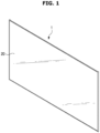
- FIG. 1 is a perspective view of a display apparatus according to an embodiment of the present disclosure
- FIG. 2 is an exploded perspective view of the display apparatus according to an embodiment of the present disclosure
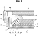
- FIG. 3 is a cross-sectional view of a portion of the display apparatus according to an embodiment of the present disclosure.
- the present disclosure illustrates a flat display apparatus 1 as an example, but may be applied to a curved display apparatus or a bendable display apparatus.
- the terms 'front' and 'front surface' used herein are based on a front surface of a display panel 20 side which displays an image, based on the display apparatus 1 illustrated in FIG. 1 .
- the terms 'upper' and 'lower' indicate an upper side and a lower side of the display apparatus 1 illustrated in FIG. 1
- the terms 'opposite sides' and 'one side' indicate the left and right directions of the display apparatus 1 illustrated in FIG. 1 .
- the display apparatus 1 includes a display module for displaying an image.
- the display module includes a display panel 20 on which an image is displayed, and a backlight unit configured to supply light to the display panel 20.
- the backlight unit may include a light source module 100 and an optical sheet 60. That is, the backlight unit may include the light source module 30 disposed in the rear of the display panel 20, a light guide panel 40 disposed in a space between the display panel 20 and the light source module 100 such that light transmitted from a rear side thereof is diffused and transmitted to the display panel 20 positioned at a front side thereof, the optical sheet 60 disposed between the light guide panel 40 and the display panel 20 to change optical properties, a middle mold 70 configured to support the display panel 20 and the light guide panel 40, and a display chassis 80 forming an outer appearance.
- the optical sheet 60 may include various sheets.
- the optical sheet 60 may include a diffusion sheet, a prism sheet, a protective sheet, and a brightness enhancing film.
- the drawings illustrate that the optical sheet 60 is configured by two sheets for convenience, the present disclosure is not limited thereto and the optical sheet 60 may be formed in a plurality of configurations as described above.
- the display chassis 80 includes a top chassis 82 coupled to a front side of the middle mold 70 to maintain a state in which the display panel 20 is installed on the middle mold 70, and a bottom chassis 84 coupled to a rear side of the middle mold 70 and in which the light source module 100 is disposed on inner opposite sides thereof.
- the light source module 100 may be disposed inside the bottom chassis 84 to irradiate light toward an inner center side of the bottom chassis 84, and in detail, toward a side surface 41 of the light guide panel 40.
- the light source module 100 is disposed at a lower portion of the display apparatus 1, but is not limited thereto, and the light source module may be applied only to at least one side of the lower portion, sides, and an upper portion of the display apparatus 1, or may be applied entirely along the display apparatus 1.
- a light source of an edge type display manner as above may be applied, or a light source of a direct type display manner may be applied.
- the light guide panel 40, the display panel 20, and the top chassis 82 are sequentially installed on the front side of the middle mold 70, and the bottom chassis 84 is installed on the rear side of the middle mold 70, so that the respective components are not only supported by the middle mold 70, but also the display panel 20 and the bottom chassis 84 are maintained in a state of being spaced apart from each other.
- the top chassis 82 includes a bezel portion 82a covering a front outer edge of the display panel 20, and a top side portion 82b bent backward from an end of the bezel portion 82a to cover a side surface of the middle mold 70.
- the bottom chassis 84 includes a rear side portion 84a forming a rear surface of the display module, and a bottom side portion 84b extending forward from an edge of the rear side portion and coupled to the inside of the middle mold 70.
- the light source module 100 may include a light source 110 and a printed circuit board 120.
- the light source 110 includes a light emitting device (LED).
- a plurality of the light source 110 may be provided, and the plurality of light source 110 may be arranged to be spaced apart from each other at a predetermined interval.
- the light source module 100 will be described later in detail.
- a heat sink 50 to dissipate heat generated from the light source module 100 may be disposed between the light source module 100 and the bottom chassis 84.
- the heat sink 50 may be configured to transfer heat generated from the light source module 100 to the bottom chassis 84 to dissipate high heat generated from the light source module 100 to the outside. Accordingly, the heat sink 50 may dissipate high heat generated by the light source module 100 to prevent malfunctions that may occur due to the high temperature of the light source module 100, thereby improving reliability of the display apparatus 1.
- the light guide panel 40 is disposed to be spaced apart from the bottom chassis 84 so that the light source 110 is disposed on opposite sides of a space between the light guide panel 40 and an inner surface of the bottom chassis 84, that is, on the bottom side portion 84b side.
- the light guide panel 40 may include a reflective member 45 on a rear surface thereof.
- the reflective member 45 may be provided on the rear surface of the light guide panel 40 so that all the light generated from the light source package 31 may direct to a front surface thereof.
- the reflective member 45 which is a reflector, may be provided separately from the light guide panel 40 and disposed on the rear surface of the light guide panel 40, or may be integrally formed with the light guide panel 40.
- a reflective coating on the rear surface of the light guide panel 40 the same effects as described above may be obtained.
- the light guide panel 40 is provided to transmit light generated from the light source.
- the light guide panel 40 may be formed of a transparent resin material. That is, light incident by the light source module 100 from the side surface 41 of the light guide panel 40 may be transmitted to a front surface of the light guide panel 40 to irradiate light to the display panel 20 side.
- the light guide panel 40 may be disposed to be spaced apart from the light source at a predetermined interval to minimize deformation due to heat generated from the light source.
- the light source module 100 will be described in detail.
- the light source module 100 may include the light source 110.
- the light source 110 may emit blue-based light. In this case, the blue-based light may be light partially biased toward green.
- the light source 110 may be formed of at least one of a blue QD-based electroluminescent device, a blue fluorescent-based electroluminescent device, a blue thermally activated delayed fluorescent-based electroluminescent device, and a blue phosphorescent-based electroluminescent device.
- the blue light generated in the light source 110 may be converted into light having a color of RGB (white, red, green, blue) through the quantum dot conversion member 120.
- the quantum dot conversion member 120 may convert the color of light emitted from the light source 110 by using quantum dots (QDs). Therefore, the quantum dot conversion member 120 may be expressed as a color adjuster.
- QDs quantum dots
- the quantum dot conversion member 120 may convert the color of the light, which is emitted from the light source 110 and incident thereon, and may emit light of different colors.
- the quantum dot converter 120 may convert blue light, which is emitted from the light source 110 and incident thereon, into red light and green light, and then emit the lights to the outside.
- the quantum dot conversion member 120 may emit light having a different color from incident light by changing the wavelength of the incident light (wavelength shift).
- Quantum dots emit light of a specific wavelength by emitting light of their own or absorbing light when a voltage is applied.
- Electrons in a quantum dot are located at a low energy level (or band) in a stable state. In this state, when the quantum dot absorbs light from the outside, electrons in the low energy level move to a high energy level (or band). Because electrons located at the high energy level are in an unstable state, the electrons naturally move from the high energy level to the low energy level. As such, while moving from the high energy level to the low energy level, the electrons emit light as much as the energy difference between the high energy level and the low energy level. In this case, the wavelength of the emitted light is determined by the energy difference between the high energy level and the low energy level.
- the smaller the size of a quantum dot may emit light of a shorter wavelength, the larger the size of a quantum dot may emit light of a longer wavelength.
- a quantum dot of about 2 nanometers (nm) in diameter may emit blue light, and a quantum dot of about 10 nanometers (nm) in diameter may emit red light.
- quantum dots of various sizes when quantum dots of various sizes are used, light of various wavelengths from red light to blue light may be output. That is, when quantum dots of various sizes are used, light having natural colors may be generated.
- the quantum dot conversion member 120 may be manufactured by dispersing the quantum dots described above in a resin. When light is incident from the light source 110 to the quantum dot conversion member 120, the incident light excites electrons of the quantum dots included in the quantum dot conversion member 120. In other words, electrons in the low energy level (or band) move to the high energy level (or band) by the incident light.
- the quantum dots output light of various wavelengths depending on the size thereof.
- light having various wavelengths may generate an image by passing through the light guide panel 40, the optical sheet 60, and the display panel 20.
- the quantum dot conversion member 120 may include green light quantum dots capable of emitting green-based light and red light quantum dots capable of emitting red-based light.
- Green light quantum dot particles 132 may be particles having a particle width of about 2 nanometers to about 3 nanometers
- red light quantum dot particles 122 may be particles having a particle width of about 5 nanometers to about 6 nanometers.
- the green-based light and the red-based light may be emitted by the green light quantum dots and the red light quantum dots.
- white light in which three lights having different wavelengths are mixed may be incident on the side surface 41 of the light guide panel 40.
- the light guide panel 40 may be configured to guide the white light incident on the side surface 41 to the front of the light guide panel 40 so that the white light is irradiated onto the display panel 20.
- the quantum dot conversion member is provided in the form of a quantum dot sheet and is disposed on the front surface of the light guide panel to convert light emitted from the front surface of the light guide panel, so that white light in which three lights having different wavelengths are mixed is emitted to the display panel side.
- the quantum dot sheet is processed with an area corresponding to the front surface of the light guide panel, but the production cost increases due to the large area to be processed.
- white light is irradiated to the display apparatus in a method in which the quantum dot conversion member is applied or attached to a surface of the light source so that the light irradiated to the light guide panel is converted into white light and then emitted to the light guide panel.
- the quantum dot conversion member is applied or attached to a surface of the light source so that the light irradiated to the light guide panel is converted into white light and then emitted to the light guide panel.
- the quantum dots of the quantum dot conversion member are changed due to high heat generated from the light source, which degrades performance. That is, the light emitting region of the quantum dots is reduced as an inorganic material surrounding the quantum dots is separated by the high heat and thus the efficiency of emitting light is reduced, thereby reducing overall performance.
- the light source module 100 may be radiated by disposing the light source 110 and the quantum dot conversion member 120 to be spaced apart from each other, and the white light formed by the quantum dot conversion member 120 and the light source 110 through the transparent member 140 disposed between the light source 110 and the quantum dot conversion member 120 may be efficiently irradiated to the side surface 41 of the light guide panel 40.
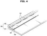
- FIG. 4 illustrates a configuration of a part of the display apparatus according to an embodiment of the present disclosure
- FIGS. 5A to 5C schematically illustrate light traveling paths in the display apparatus according to an embodiment of the present disclosure
- FIG. 6 schematically illustrates the flow of heat in the display apparatus according to an embodiment of the present disclosure.
- the light source 110 and the quantum dot conversion member 120 may be mounted on a printed circuit board 130.
- the printed circuit board 130 may include a metal material.
- the printed circuit board 130 may include a flat portion 131 provided in parallel with the rear surface of the light guide panel 40 and extending from the rear surface of the light guide panel 40 to the side surface 41, and an inclined portion 132 extending to be inclined from one side of the flat portion 131 with respect to the side surface 41 of the light guide panel 40.
- the light source 110 may be mounted on the inclined portion 132, and the quantum dot conversion member 120 may be mounted on the flat portion 131.
- the flat portion 131 may be disposed to be orthogonal to the side surface 41 of the light guide panel 40, and the inclined portion 132 may be disposed to be inclined with respect to the side surface 41 of the light guide panel 40. Accordingly, the quantum dot conversion member 120 disposed on the flat portion 131 may be disposed to be orthogonal to the side surface 41 of the light guide panel 40, and the light source 110 disposed on the inclined portion 132 may be disposed to be inclined with respect to the side surface 41 of the light guide panel 40.
- the printed circuit board 130 may include a first region (inclined portion) formed to be inclined with respect to the light guide panel 40, and a second region (flat portion) extending from one end of the first region toward the light guide panel 40.
- the first region is disposed to be inclined with respect to the side surface 41 of the light guide panel 40 and may extend from one end of the first region, which is positioned furthest from the side surface of the light guide panel 40, toward the side surface 41 of the light guide panel 40.
- the second region may be disposed in parallel with the light guide panel 40. That is, the second region may be disposed in parallel with the front and rear surfaces of the light guide panel 40.
- the light source 110 and the quantum dot conversion member 120 may be disposed to be spaced apart from each other on the printed circuit board 130. Accordingly, high heat generated from the light source 110 may be prevented from being transferred to the quantum dot conversion member 120.
- one part L2 of blue light emitted from the light source 110 may be advanced to the quantum dot conversion member 120 and converted on the quantum dot conversion member 120, and then red light and green light may be emitted.
- the quantum dot conversion member 120 may be manufactured by dispersing a plurality of red light quantum dots and a plurality of green light quantum dots in a resin. Accordingly, the plurality of quantum dots may be formed in a layer form.
- the quantum dot conversion member 120 may include a reflective layer 122 disposed below the quantum dot layer 121 such that light converted in the quantum dot layer 121 may be reflected. That is, the part L2 of the blue light emitted from the light source 110 may be converted into green light or red light by a plurality of quantum dots and reflected by the reflective layer 122 to change a traveling direction thereof.
- the other part L1 of the blue light emitted from the light source 110 and the red light and green light L2 reflected from the quantum dot conversion member 120 are mixed to form white light, and the mixed white light may be incident on the side surface 41 of the light guide panel 40. That is, the other part L1 of the blue light emitted from the light source 110 may be directly irradiated to the side surface 41 of the light guide panel 40, and the red light and green light L2 reflected from the quantum dot conversion member 120 may be irradiated to the side surface 41 of the light guide panel 40.
- the light source 110 is mounted on the inclined portion 131 so that a large amount of light L2 is emitted toward the quantum dot conversion member 120, because the amount of light L1 emitted directly toward the side surface 41 of the light guide panel 40 is also large, the light incident on the light guide panel 40 finally may be formed as white light including a large amount of blue light.
- the light source module 100 may include a transparent member 140 configured to transmit only a part of the light emitted from the light source 110 and the quantum dot conversion member 120 to the side surface 41 of the light guide panel 40.
- the transparent member 140 may transmit one parts L3 and L5 of light incident on a transparent portion of the transparent member 140 and may reflect the other parts L4 and L6 of light to change the path of the light.
- the transparent member 140 may guide a path of light directing directly from the light source 110 to the light guide panel 40 such that the light may direct back to the light guide panel 40 after transmitting the quantum dot conversion member 120 by particularly reflecting the light directing directly from the light source 110 to the light guide panel 40, to the opposite side.
- the amount of light L2 emitted from the light source 110 toward the quantum dot conversion member 120 may be partially adjusted by adjusting an inclination angle of the inclined portion 132 with respect to the flat portion 131 without the transparent member 140, all paths of light emitted in all directions through the inclination angle of the inclined portion 132 may not be adjusted.
- the light source module 100 includes the transparent member 140 and may be configured such that high-definition white light is incident on the light guide panel 40 by adjusting a ratio of blue light, green light, and red light as the path of light transmitted through the transparent member 140 is guided.
- the transparent member 140 is disposed between the light source 110 and the quantum dot conversion member 120.
- the transparent member 140 is disposed between the light source 110 and the side surface 41 of the quantum dot conversion member 120 and the light guide panel 40 and may be configured such that the light L1 emitted from the light source 110 and the light L2 reflected through the quantum dot conversion member 120 are incident on the side surface 41 of the light guide panel 40 by being transmitted through the transparent member 140.
- the transparent member 140 has a triangular pillar shape.
- the transparent member 140 may be provided to extend along a direction in which the plurality of light sources 110 is disposed.
- the transparent member 140 includes a first surface 141 disposed to correspond to the light source 110, a second surface 142 disposed to correspond to the quantum dot conversion member 120, and a third surface 143 disposed adjacent to the side surface 41 of the light guide panel 40.
- the first surface 141, the second surface 142, and the third surface 143 form the triangular pillar shape of the transparent member 140.
- the transparent member 140 may include a transparent material through which light may be transmitted.
- the transparent member 140 may be formed of a material such as acrylic, silicone, and PET.
- the first surface 141 may be disposed substantially parallel to the light source 110 and adjacent to the light source 110. That is, the first surface 141 may be disposed to be inclined with respect to the side surface 41 of the light guide panel 40 at approximately the same angle as the light source 110 and the inclined portion 132. In other words, the first surface 141 may be provided to face the light source 110.
- the first surface 141 may be formed such that light emitted from the light source 110 may be transmitted into the transparent member 140. The light transmitted through the first surface 141 may be incident on the second surface 142 or the third surface 143 in the transparent member 140.
- the second surface 142 may be disposed substantially parallel to the quantum dot conversion member 120 and adjacent to the quantum dot conversion member 120.
- first surface 141 and one end of the second surface 142 may be disposed to be in contact with each other, and thus the inclination angle may be formed between the first surface 141 and the second surface 142. That is, the first surface 141 and the second surface 142 may be arranged to have an inclination angle ⁇ corresponding to the inclination angle between the light source 110 or the inclined portion 132 and the quantum dot conversion member 120 or flat portion 131.
- the one part L2 of the light transmitted through the first surface 141 may be incident to the second surface 142 in the transparent member 140.
- the light L2 incident on the second surface 142 may be transmitted through the second surface 142 and incident on the quantum dot conversion member 120.
- the other part L2 of the light emitted from the light source 110 may be incident on the quantum dot conversion member 120 through the first surface 141 and the second surface 142.
- the light L2 incident on the quantum dot conversion member 120 may be incident on the second surface 142 again by being reflected after being converted.
- the light incident on the second surface 142 may travel toward the first surface 141 or the third surface 143 in the transparent member 140.
- the third surface 143 may be disposed such that the other end of the first surface 141 and the other end of the second surface 142 are connected to each other.
- the third side 143 is disposed adjacent to the side surface 41 of the light guide panel 40 and may be a transmission surface through which light incident on the transparent member 140 by the light source 110 and the quantum dot conversion member 120 is finally transmitted toward the light guide panel 40.
- the light L1 directly incident from the light source 110, the light L2 reflected by the quantum dot conversion member 120, or the light reflected through the quantum dot conversion member 120 and then reflected in the transparent member 140 again may be incident on the third surface 143 and finally pass through the outside of the transparent member 140 to travel to the light guide panel 40.
- the lights L4 and L6 incident on the third surface 143 at an incidence angle larger than a predetermined incidence angle among the light incident on the third surface 143 may be reflected by the third surface 143. That is, the at least one parts L3 and 5 of the light incident on the third surface 143 are transmitted toward the light guide panel 40, and the other parts L4 and L6 of the light may not be transmitted through the third surface 143 and may be reflected to the inside of the transparent member 140.
- the light L4 incident on the third surface 143 at an incidence angle larger than the predetermined incidence angle with respect to the third surface 143 among the light L1 directing directly to the light guide panel 40 from the light source 110 may not be transmitted through the third surface 143 and may be reflected to the inside of the transparent member 140 by the third surface 143.
- the light L4 reflected by the third surface 143 may be changed in direction to travel toward the quantum dot conversion member 120 and may be directly incident (light L4') to the third surface 143 again by being reflected after being converted by the quantum dot conversion member 120, or may be incident (light L4") to the third surface 143 after additional reflection in the transparent member 140.
- the light reflected by the third surface 143 may be incident to the quantum dot conversion member 120 side through additional reflection inside the transparent member 140 after the direction thereof is changed.
- the light converted after being incident on the quantum dot conversion member 120 through additional reflection may be incident directly to the third surface 143 by being reflected, or may be incident to the third surface 143 after additional reflection inside the transparent member 140.
- the light L3 incident on the third surface 143 at an incidence angle smaller than the predetermined incidence angle among the light incident directly on the third surface 143 from the light source 110 may not be reflected by the third surface 143 and may pass through the third surface 143 to travel toward the light guide panel 40. Because the light L3 transmitted through the third surface 143 has passed through the transparent member 140 without passing through the quantum dot conversion member 120, blue light emitted from the light source 110 may be maintained.
- the light L2 directing to the quantum dot conversion member 120 from the light source 110 may be reflected after the property of the light is converted in the quantum dot conversion member 120 and may direct to the third surface 143.
- the light L5 incident on the third surface 143 with an incidence angle smaller than the predetermined incidence angle among the light reflected on the third surface 143 may be transmitted through the third surface 143 to be irradiated to the side surface 41 of the light guide panel 40, and the light L6 incident on the third surface 143 with an incidence angle larger than the predetermined incidence angle may not be transmitted through the third surface 143, may be reflected by the third surface 143 and reflected again inside the transparent member 140, and then incident (light L6') again to the third surface 143.
- An interspace 150 which is a space through which light transmitted through the transparent member 140 travels to the light guide panel 40, may be provided between the transparent member 140 and the light guide panel 40.
- the interspace 150 may be a space that does not include a medium other than air.
- the interspace 150 is provided between the third surface 143 of the transparent member 140 and the light guide panel 40, and by the interspace 150 the light L4 and L6 incident on the third surface 143 at an angle larger than or equal to the predetermined incidence angle may not be transmitted through the third surface 143 and may be reflected.
- the density of a medium in the transparent member 140 is greater than the density of a medium in the interspace 150, when the light is incident on the third surface 143 at an angle larger than the predetermined incidence angle, the light may not be transmitted through the third surface 143.
- the predetermined incidence angle may vary depending on the type of material included in the transparent member 140. Because the medium of the interspace 150 is limited to air, the incidence angle at which light may be transmitted through the third surface 143 may be changed due to a density difference from the medium of the transparent member 140. For example, when the transparent member 140 is formed of an acrylic material, the predetermined incidence angle with respect to the third surface 143 may be about 30 degrees, and when the transparent member 140 is formed of a silicon material, the predetermined incidence angle with respect to the third surface 143 may be about 25 degrees.
- An inclination angle ⁇ between the light source 110 and the quantum dot conversion member 120 or the inclination angle ⁇ between the first surface 141 and the second surface 142 may be in the range of about 35 and 75 degrees. It may be appropriate that the inclination angle ⁇ may be about 55 degrees.
- Light emitted from the light source 110 may be efficiently incident on the light guide panel 40 by directly passing through the transparent member 140 or by passing through the transparent member 140 via the quantum dot conversion member 120 within the range of the inclination angle ⁇ described above.
- the inclination angle ⁇ may be determined in consideration of an angle at which light emitted from the light source 110 is directly incident on the third surface 143 and an angle at which light emitted from the light source 110 is reflected from the quantum dot conversion member 120 and incident on the third surface 143.
- the predetermined incidence angle at which light may pass through the third surface 143 may be determined according to the type of the medium of the transparent member 140, and the ratio of the blue light emitted directly to the third surface 143 from the light source 110 and the red light and green light converted by the quantum dot conversion member 120 may be different according to the predetermined incidence angle with respect to the third surface 143, and thus together with the above considerations, the inclination angle ⁇ may be determined in consideration of the predetermined incidence angle.
- a reflective sheet 160 configured to reflect light directing to the outside of the side surface 41 of the light guide panel 40 among the light transmitted through the transparent member 140 to the side surface 41 of the light guide panel 40 may be disposed on one side of the interspace 150.
- the reflective sheet 160 may be disposed between the transparent member 140 and the side surface 41 of the light guide panel 40 inside the interspace 150.
- the reflective sheet 160 may be configured to extend from an end portion of the inclined portion 132 adjacent to the light guide panel 40 to at least a portion of the front surface of the light guide panel 40 adjacent to the side surface 41 of the light guide panel 40.
- the reflective sheet reflects light directly directing to the direction in which the optical sheet 60 is disposed among the light transmitted from the transparent member 140 and irradiates light to the side surface 41 of the light guide panel 40, thereby minimizing light loss.
- the light source 110 and the quantum dot conversion member 120 are disposed to be spaced apart from each other by the transparent member 140, high-definition white light may be irradiated to the light guide panel 40.
- the high heat generated from the light source 110 is not directly transferred to the quantum dot conversion member 120, so that the degradation of the efficiency of the quantum dot conversion member 120 caused by changing the characteristics of a plurality of quantum dots of the quantum dot conversion member 120 due to high heat may be prevented.
- high heat generated from the light source 110 may be directly transferred to the quantum dot conversion member 120 when the quantum dot conversion member 120 is disposed in contact with the light source 110 as in the conventional case, as illustrated in FIG. 6 , high heat H1 generated from the light source 110 of the light source module 100 according to an embodiment of the present disclosure is not directly transmitted to the quantum dot conversion member 120 and may be dissipated by moving to the heat sink 50 disposed on a rear side of the printed circuit board 130 along the printed circuit board 130.
- heat H2 may be generated in the process of converting light in the quantum dot conversion member 120
- the quantum dot conversion member 120 is disposed adjacent to the heat sink 50, and heat generated from the quantum dot conversion member 120 is directly transferred to the heat sink 50 through the printed circuit board 130, thereby facilitating heat dissipation.
- the quantum dot conversion member 120 provided in a sheet shape, as a surface of the sheet is provided in contact with the printed circuit board 130, the path through which the heat is transferred is shortly formed and the internal resistance is minimized, thereby preventing high temperature from being generated in the quantum dot conversion member 120.
- the transparent member 140 provided between the light source 110 and the quantum dot conversion member 120 may be formed of a resin such as acrylic and silicone and such a resin material has a low thermal conductivity, and thus may serve as an insulating member preventing heat generated from the light source 110 from being transferred to the quantum dot conversion member 120 through the transparent member 140.
- the heat generated from the light source 110 is not transferred to the quantum dot conversion member 120 through the transparent member 140, but may be transferred to the heat sink 50 along the printed circuit board 130 to be dissipated.
- a light source module 100' of the display apparatus 1 will be described. Because configurations other than the light source module 100' described below are the same as in the display apparatus 1 according to an embodiment of the present disclosure, overlapping descriptions are omitted.
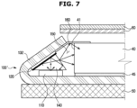
- FIG. 7 schematically illustrates light traveling paths in a display apparatus according to another embodiment of the present disclosure
- FIG. 8 schematically illustrates the flow of heat in a display apparatus according to another embodiment of the present disclosure.
- the light source 110 may be disposed on the flat portion 131 of the printed circuit board 130 of the light source module 100' according to another embodiment of the present disclosure. Accordingly, the quantum dot conversion member 120 may be disposed on the inclined portion 132 of the printed circuit board 130.
- a part of the blue light emitted from the light source 110 disposed on the flat portion 131 may pass through the transparent member 140 to be irradiated to the side surface 41 of the light guide panel 40, and the other part of the blue light emitted from the light source 110 may reach the quantum dot conversion member 120 to be converted into red light or green light and then may pass through the transparent member 140 to be irradiated to the side surface 41 of the light guide panel 40.
- the process of reflecting light inside the transparent member 140 is the same as the process of reflecting light inside the transparent member 140 of the light source module 100 according to an embodiment of the present disclosure except that only the direction of light is changed, and thus description thereof is omitted.
- the high heat H1 generated from the light source 110 disposed on the flat portion 131 may be transferred to the heat sink 50 disposed on a rear surface of the flat portion 131 through the printed circuit board 130 to be dissipated.
- the light source 110 of the light source module 100' is disposed adjacent to the heat sink 50, thereby improving heat dissipation efficiency. Accordingly, the high heat H1 generated from the light source 110 is efficiently radiated, so that the efficiency and reliability of the light source 110 may be improved.
- the quantum dot conversion member 120 disposed in the inclined portion 132 and the light source 110 disposed in the flat portion 131 are disposed to be spaced apart from each other, so that the high heat H1 generated from the light source 110 is not directly transferred to the quantum dot conversion member 120.
- a thermal conductivity of the transparent member disposed between the light source 110 and the quantum dot conversion member 120 is small, heat generated from the light source 110 is not transferred to the quantum dot conversion member 120 through the transparent member 140 and may be directly transferred to the heat sink 50 through the printed circuit board 130.
- the heat H2 When light is incident on the quantum dot conversion member 120, the heat H2 may be generated as the properties of the light change, and the heat H2 generated may be transferred to the flat portion 131 along the inclined portion 132 and then transferred to the heat sink 50 to dissipate heat.
Description
- The present disclosure relates to a display apparatus, and more particularly, to a display apparatus including an improved backlight unit.
- In general, a display apparatus is a device for displaying an image, such as a monitor or a television. A self-light emitting display panel, such as an organic light-emitting diode (OLED), or a light-receiving/emitting display panel, such as a liquid crystal display (LCD) panel, is used in a display apparatus.
- The present disclosure relates to a display module and display apparatus to which a light-receiving/emitting display panel is applied. The display apparatus to which a light-receiving/emitting display panel is applied includes a display panel consisting of a liquid crystal panel and displaying an image, and a backlight unit supplying light to the display panel, and the backlight unit includes a light source module having a light source, and a plurality of optical sheets and a light guide panel receiving light from the light source and guiding the light to the display panel, and the like.
- In the existing display apparatuses, light emitted from a light source may improve color reproducibility through quantum dots (QDs). In the existing display apparatuses, such color reproducibility is implemented through a quantum dot sheet (QD sheet) provided at the rear of the display panel, which may cause cost increase of the display apparatus and problems in assembly.
-
US2017269279 describes a reflective filter serving as a multi-bandpass filter for a light source configured to emit light in a plurality of color primary wavelengths to improve color purity. The reflective filter comprises conversion materials that are disposed on substrates which are arranged in a triangular shape. The reflective filter is arranged between a light source and a backlight of a display panel. -
JP2011082590 US20130286327A1 describes a backlight module configured with a waveguide including an incident surface, and a refractive surface adjacent to the incident surface, and a bottom surface opposite to the refractive surface.KR1020170036972A -
US20160266299A1 describes a backlight unit that may be used with a liquid crystal display. - The present disclosure is directed to providing a display apparatus with an improved structure to improve color reproducibility.
- The present disclosure is directed to providing a display apparatus capable of maintaining color reproduction performance while minimizing a quantum dot conversion member.
- One aspect of the present disclosure provides a display apparatus including a display panel, a light guide panel disposed in the rear of the display panel, a light source disposed adjacent to a side surface of the light guide panel, a quantum dot conversion member disposed to be inclined with respect to the light source, including quantum dot particles, and configured to convert properties of light emitted from the light source, and a transparent member including a first surface facing the light source, a second surface facing the quantum dot conversion member, and a third surface disposed adjacent to the side surface of the light guide panel, wherein the transparent member is configured to transmit at least one part of the light incident on the third surface to the side surface of the light guide panel and reflect the other part of the light to the inside thereof.
- The transparent member includes a triangular pillar shape formed by the first surface, the second surface and the third surface, and the transparent member may be disposed between the light source and the quantum dot conversion member.
- The first surface and the second surface may be disposed to be inclined at about 35 degrees to 75 degrees.
- The light source may be disposed substantially parallel to the first surface, and the quantum dot conversion member may be disposed substantially parallel to the second surface.
- The first surface may be configured to allow light emitted from the light source to be incident and to allow the incident light to be transmitted through the second surface or the third surface.
- The second surface may be configured to allow light transmitted from the first surface or reflected from the third surface to be transmitted to the quantum dot conversion member, and to allow light converted by the quantum dot conversion member to be incident again and allow the converted light to be transmitted to the first surface or the third surface.
- The third surface may be configured to allow light incident at a predetermined angle among light incident through the first surface or the second surface to be transmitted to the side surface of the light guide panel and to allow light incident at an angle larger than the predetermined angle to be reflected toward the first surface or the second surface.
- The predetermined angle may be in the range of 60 to 80 degrees.
- The display apparatus may further include a printed circuit board on which the light source and the quantum dot conversion member are mounted and a heat sink disposed in contact with the printed circuit board, and heat generated from the quantum dot conversion member may be directly transferred to the heat sink through the printed circuit board.
- The transparent member may be configured to limit heat generated from the light source to be transferred to the quantum dot conversion member.
- The printed circuit board may include a flat portion disposed parallel to the light guide panel and an inclined portion extending to be inclined with respect to the flat portion.
- The quantum dot conversion member may be disposed on the flat portion, and the light source may be disposed on the inclined portion.
- The quantum dot conversion member may be disposed on the inclined portion, and the light source may be disposed on the flat portion.
- The quantum dot conversion member may be disposed on a front surface of the flat portion, and the heat sink may be disposed on a rear surface of the flat portion.
- The display apparatus may further include an interspace formed between the third surface and the side surface of the light guide panel and configured to allow light transmitted from the third surface to move to the side surface of the light guide panel, and a reflective member disposed on one side of the interspace and configured to reflect light traveling from the interspace to the outside of the side surface of the light guide panel toward the side surface of the light guide panel.
- Another aspect of the present disclosure provides a display apparatus including a display panel, a light guide panel disposed in the rear of the display panel, a light source disposed on a side surface of the light guide panel, a quantum dot conversion member including quantum dot particles and configured to convert properties of light emitted from the light source, a printed circuit board including an inclined portion on which the light source is disposed and configured to be inclined with respect to a side surface of the light guide panel, and a flat portion on which the quantum dot conversion member is disposed and configured to be disposed parallel to the light guide panel, and a transparent member disposed between the light source and the quantum dot conversion member and configured to transmit light emitted from the light source and light converted by the quantum dot conversion member to the side surface of the light guide panel.
- The present disclosure directs to improve color reproducibility in a display apparatus that displays an image using light incident from a backlight unit.
- In the present disclosure, a light source and a quantum dot conversion member are arranged to be spaced apart from each other and to be inclined so that the quantum dot conversion member can be prevented from being damaged by heat generated from the light source, and a transparent member is disposed between the light source and the quantum dot conversion member so that the light emitted from the light source and the light converted by the quantum dot conversion member can be effectively transmitted to a light guide panel.
-
-
FIG. 1 is a perspective view of a display apparatus according to an embodiment of the present disclosure. -
FIG. 2 is an exploded perspective view of the display apparatus according to an embodiment of the present disclosure. -
FIG. 3 is a cross-sectional view of a portion of the display apparatus according to an embodiment of the present disclosure. -
FIG. 4 illustrates a configuration of a part of the display apparatus according to an embodiment of the present disclosure. -
FIG. 5 schematically illustrates light traveling paths in the display apparatus according to an embodiment of the present disclosure. -
FIG. 6 schematically illustrates the flow of heat in the display apparatus according to an embodiment of the present disclosure. -
FIG. 7 schematically illustrates light traveling paths in a display apparatus according to another embodiment of the present disclosure. -
FIG. 8 schematically illustrates the flow of heat in a display apparatus according to another embodiment of the present disclosure. - The embodiments described in the present specification and the configurations shown in the drawings are only examples of preferred embodiments of the present disclosure, and various modifications may be made at the time of filing of the present disclosure to replace the embodiments and drawings of the present specification.
- Like reference numbers or signs in the various drawings of the application represent parts or components that perform substantially the same functions.
- The terms used herein are for the purpose of describing the embodiments and are not intended to restrict and/or to limit the present disclosure. For example, the singular expressions herein may include plural expressions, unless the context clearly dictates otherwise. Also, the terms "comprises" and "has" are intended to indicate that there are features, numbers, steps, operations, elements, parts, or combinations thereof described in the specification, and do not exclude the presence or addition of one or more other features, numbers, steps, operations, elements, parts, or combinations thereof.
- It will be understood that, although the terms first, second, etc. may be used herein to describe various components, these components should not be limited by these terms. These terms are only used to distinguish one component from another. For example, without departing from the scope of the present disclosure, the first component may be referred to as a second component, and similarly, the second component may also be referred to as a first component. The term "and/or" includes any combination of a plurality of related items or any one of a plurality of related items.
- Hereinafter, embodiments of the present disclosure will be described in detail with reference to the accompanying drawings.
-
FIG. 1 is a perspective view of a display apparatus according to an embodiment of the present disclosure,FIG. 2 is an exploded perspective view of the display apparatus according to an embodiment of the present disclosure, andFIG. 3 is a cross-sectional view of a portion of the display apparatus according to an embodiment of the present disclosure. - The present disclosure illustrates a
flat display apparatus 1 as an example, but may be applied to a curved display apparatus or a bendable display apparatus. - The terms 'front' and 'front surface' used herein are based on a front surface of a
display panel 20 side which displays an image, based on thedisplay apparatus 1 illustrated inFIG. 1 . Based on the above, the terms 'upper' and 'lower' indicate an upper side and a lower side of thedisplay apparatus 1 illustrated inFIG. 1 , and the terms 'opposite sides' and 'one side' indicate the left and right directions of thedisplay apparatus 1 illustrated inFIG. 1 . - The
display apparatus 1 includes a display module for displaying an image. - The display module includes a
display panel 20 on which an image is displayed, and a backlight unit configured to supply light to thedisplay panel 20. The backlight unit may include alight source module 100 and anoptical sheet 60. That is, the backlight unit may include the light source module 30 disposed in the rear of thedisplay panel 20, alight guide panel 40 disposed in a space between thedisplay panel 20 and thelight source module 100 such that light transmitted from a rear side thereof is diffused and transmitted to thedisplay panel 20 positioned at a front side thereof, theoptical sheet 60 disposed between thelight guide panel 40 and thedisplay panel 20 to change optical properties, amiddle mold 70 configured to support thedisplay panel 20 and thelight guide panel 40, and adisplay chassis 80 forming an outer appearance. - The
optical sheet 60 may include various sheets. For example, theoptical sheet 60 may include a diffusion sheet, a prism sheet, a protective sheet, and a brightness enhancing film. The drawings (FIGS. 2 and3 ) illustrate that theoptical sheet 60 is configured by two sheets for convenience, the present disclosure is not limited thereto and theoptical sheet 60 may be formed in a plurality of configurations as described above. - The
display chassis 80 includes atop chassis 82 coupled to a front side of themiddle mold 70 to maintain a state in which thedisplay panel 20 is installed on themiddle mold 70, and abottom chassis 84 coupled to a rear side of themiddle mold 70 and in which thelight source module 100 is disposed on inner opposite sides thereof. - The
light source module 100 may be disposed inside thebottom chassis 84 to irradiate light toward an inner center side of thebottom chassis 84, and in detail, toward aside surface 41 of thelight guide panel 40. In an embodiment of the present disclosure, thelight source module 100 is disposed at a lower portion of thedisplay apparatus 1, but is not limited thereto, and the light source module may be applied only to at least one side of the lower portion, sides, and an upper portion of thedisplay apparatus 1, or may be applied entirely along thedisplay apparatus 1. A light source of an edge type display manner as above may be applied, or a light source of a direct type display manner may be applied. - The
light guide panel 40, thedisplay panel 20, and thetop chassis 82 are sequentially installed on the front side of themiddle mold 70, and thebottom chassis 84 is installed on the rear side of themiddle mold 70, so that the respective components are not only supported by themiddle mold 70, but also thedisplay panel 20 and thebottom chassis 84 are maintained in a state of being spaced apart from each other. - The
top chassis 82 includes abezel portion 82a covering a front outer edge of thedisplay panel 20, and atop side portion 82b bent backward from an end of thebezel portion 82a to cover a side surface of themiddle mold 70. - The
bottom chassis 84 includes arear side portion 84a forming a rear surface of the display module, and abottom side portion 84b extending forward from an edge of the rear side portion and coupled to the inside of themiddle mold 70. - The
light source module 100 may include alight source 110 and a printedcircuit board 120. - The
light source 110 includes a light emitting device (LED). A plurality of thelight source 110 may be provided, and the plurality oflight source 110 may be arranged to be spaced apart from each other at a predetermined interval. Thelight source module 100 will be described later in detail. - A
heat sink 50 to dissipate heat generated from thelight source module 100 may be disposed between thelight source module 100 and thebottom chassis 84. Theheat sink 50 may be configured to transfer heat generated from thelight source module 100 to thebottom chassis 84 to dissipate high heat generated from thelight source module 100 to the outside. Accordingly, theheat sink 50 may dissipate high heat generated by thelight source module 100 to prevent malfunctions that may occur due to the high temperature of thelight source module 100, thereby improving reliability of thedisplay apparatus 1. - The
light guide panel 40 is disposed to be spaced apart from thebottom chassis 84 so that thelight source 110 is disposed on opposite sides of a space between thelight guide panel 40 and an inner surface of thebottom chassis 84, that is, on thebottom side portion 84b side. - The
light guide panel 40 may include areflective member 45 on a rear surface thereof. Thereflective member 45 may be provided on the rear surface of thelight guide panel 40 so that all the light generated from the light source package 31 may direct to a front surface thereof. Thereflective member 45, which is a reflector, may be provided separately from thelight guide panel 40 and disposed on the rear surface of thelight guide panel 40, or may be integrally formed with thelight guide panel 40. In addition, by applying a reflective coating on the rear surface of thelight guide panel 40, the same effects as described above may be obtained. - The
light guide panel 40 is provided to transmit light generated from the light source. To this end, thelight guide panel 40 may be formed of a transparent resin material. That is, light incident by thelight source module 100 from theside surface 41 of thelight guide panel 40 may be transmitted to a front surface of thelight guide panel 40 to irradiate light to thedisplay panel 20 side. Thelight guide panel 40 may be disposed to be spaced apart from the light source at a predetermined interval to minimize deformation due to heat generated from the light source. - Hereinafter, the
light source module 100 will be described in detail. - The
light source module 100 may include thelight source 110. Thelight source 110 may emit blue-based light. In this case, the blue-based light may be light partially biased toward green. Thelight source 110 may be formed of at least one of a blue QD-based electroluminescent device, a blue fluorescent-based electroluminescent device, a blue thermally activated delayed fluorescent-based electroluminescent device, and a blue phosphorescent-based electroluminescent device. - The blue light generated in the
light source 110 may be converted into light having a color of RGB (white, red, green, blue) through the quantumdot conversion member 120. - The quantum
dot conversion member 120 may convert the color of light emitted from thelight source 110 by using quantum dots (QDs). Therefore, the quantumdot conversion member 120 may be expressed as a color adjuster. - The quantum
dot conversion member 120 may convert the color of the light, which is emitted from thelight source 110 and incident thereon, and may emit light of different colors. For example, thequantum dot converter 120 may convert blue light, which is emitted from thelight source 110 and incident thereon, into red light and green light, and then emit the lights to the outside. In detail, the quantumdot conversion member 120 may emit light having a different color from incident light by changing the wavelength of the incident light (wavelength shift). - Quantum dots emit light of a specific wavelength by emitting light of their own or absorbing light when a voltage is applied.
- Electrons in a quantum dot are located at a low energy level (or band) in a stable state. In this state, when the quantum dot absorbs light from the outside, electrons in the low energy level move to a high energy level (or band). Because electrons located at the high energy level are in an unstable state, the electrons naturally move from the high energy level to the low energy level. As such, while moving from the high energy level to the low energy level, the electrons emit light as much as the energy difference between the high energy level and the low energy level. In this case, the wavelength of the emitted light is determined by the energy difference between the high energy level and the low energy level.
- In particular, the smaller the size of a quantum dot may emit light of a shorter wavelength, the larger the size of a quantum dot may emit light of a longer wavelength. For example, a quantum dot of about 2 nanometers (nm) in diameter may emit blue light, and a quantum dot of about 10 nanometers (nm) in diameter may emit red light.
- In addition, when quantum dots of various sizes are used, light of various wavelengths from red light to blue light may be output. That is, when quantum dots of various sizes are used, light having natural colors may be generated.
- The quantum
dot conversion member 120 may be manufactured by dispersing the quantum dots described above in a resin. When light is incident from thelight source 110 to the quantumdot conversion member 120, the incident light excites electrons of the quantum dots included in the quantumdot conversion member 120. In other words, electrons in the low energy level (or band) move to the high energy level (or band) by the incident light. - Thereafter, while the excited electrons move from the high energy level to the low energy level, the quantum dots output light of various wavelengths depending on the size thereof. As such, light having various wavelengths may generate an image by passing through the
light guide panel 40, theoptical sheet 60, and thedisplay panel 20. - The quantum
dot conversion member 120 may include green light quantum dots capable of emitting green-based light and red light quantum dots capable of emitting red-based light. Green lightquantum dot particles 132 may be particles having a particle width of about 2 nanometers to about 3 nanometers, and red lightquantum dot particles 122 may be particles having a particle width of about 5 nanometers to about 6 nanometers. - Accordingly, when the blue-based light emitted from the
light source 110 is incident on the quantumdot conversion member 120, the green-based light and the red-based light may be emitted by the green light quantum dots and the red light quantum dots. - Finally, by the blue light emitted from the
light source 110 and the green light and the red light emitted from the quantumdot conversion member 120, white light in which three lights having different wavelengths are mixed may be incident on theside surface 41 of thelight guide panel 40. - The
light guide panel 40 may be configured to guide the white light incident on theside surface 41 to the front of thelight guide panel 40 so that the white light is irradiated onto thedisplay panel 20. - In the case of a display apparatus using a conventional quantum dot conversion member, the quantum dot conversion member is provided in the form of a quantum dot sheet and is disposed on the front surface of the light guide panel to convert light emitted from the front surface of the light guide panel, so that white light in which three lights having different wavelengths are mixed is emitted to the display panel side. In this case, the quantum dot sheet is processed with an area corresponding to the front surface of the light guide panel, but the production cost increases due to the large area to be processed.
- In addition, in the case of a conventional display apparatus for solving the above problem, white light is irradiated to the display apparatus in a method in which the quantum dot conversion member is applied or attached to a surface of the light source so that the light irradiated to the light guide panel is converted into white light and then emitted to the light guide panel. In this case, however, although the area where the quantum dot conversion member is applied or adhered is considerably reduced compared to the conventional method so that the production cost is significantly reduced, the characteristics of the quantum dots of the quantum dot conversion member are changed due to high heat generated from the light source, which degrades performance. That is, the light emitting region of the quantum dots is reduced as an inorganic material surrounding the quantum dots is separated by the high heat and thus the efficiency of emitting light is reduced, thereby reducing overall performance.
- In order to solve the above problems, the
light source module 100 according to an embodiment of the present disclosure may be radiated by disposing thelight source 110 and the quantumdot conversion member 120 to be spaced apart from each other, and the white light formed by the quantumdot conversion member 120 and thelight source 110 through thetransparent member 140 disposed between thelight source 110 and the quantumdot conversion member 120 may be efficiently irradiated to theside surface 41 of thelight guide panel 40. - Hereinafter, the configuration of the
light source module 100 and the process of transmitting the light to thelight guide panel 40 will be described in detail. -
FIG. 4 illustrates a configuration of a part of the display apparatus according to an embodiment of the present disclosure,FIGS. 5A to 5C schematically illustrate light traveling paths in the display apparatus according to an embodiment of the present disclosure, andFIG. 6 schematically illustrates the flow of heat in the display apparatus according to an embodiment of the present disclosure. - As illustrated in
FIGS. 4 and5A , thelight source 110 and the quantumdot conversion member 120 may be mounted on a printedcircuit board 130. The printedcircuit board 130 may include a metal material. In detail, the printedcircuit board 130 may include aflat portion 131 provided in parallel with the rear surface of thelight guide panel 40 and extending from the rear surface of thelight guide panel 40 to theside surface 41, and aninclined portion 132 extending to be inclined from one side of theflat portion 131 with respect to theside surface 41 of thelight guide panel 40. Thelight source 110 may be mounted on theinclined portion 132, and the quantumdot conversion member 120 may be mounted on theflat portion 131. - That is, the
flat portion 131 may be disposed to be orthogonal to theside surface 41 of thelight guide panel 40, and theinclined portion 132 may be disposed to be inclined with respect to theside surface 41 of thelight guide panel 40. Accordingly, the quantumdot conversion member 120 disposed on theflat portion 131 may be disposed to be orthogonal to theside surface 41 of thelight guide panel 40, and thelight source 110 disposed on theinclined portion 132 may be disposed to be inclined with respect to theside surface 41 of thelight guide panel 40. - In other words, the printed
circuit board 130 may include a first region (inclined portion) formed to be inclined with respect to thelight guide panel 40, and a second region (flat portion) extending from one end of the first region toward thelight guide panel 40. - The first region is disposed to be inclined with respect to the
side surface 41 of thelight guide panel 40 and may extend from one end of the first region, which is positioned furthest from the side surface of thelight guide panel 40, toward theside surface 41 of thelight guide panel 40. The second region may be disposed in parallel with thelight guide panel 40. That is, the second region may be disposed in parallel with the front and rear surfaces of thelight guide panel 40. - The
light source 110 and the quantumdot conversion member 120 may be disposed to be spaced apart from each other on the printedcircuit board 130. Accordingly, high heat generated from thelight source 110 may be prevented from being transferred to the quantumdot conversion member 120. - As the
light source 110 is disposed to be inclined with respect to the quantumdot conversion member 120, one part L2 of blue light emitted from thelight source 110 may be advanced to the quantumdot conversion member 120 and converted on the quantumdot conversion member 120, and then red light and green light may be emitted. - As described above, the quantum
dot conversion member 120 may be manufactured by dispersing a plurality of red light quantum dots and a plurality of green light quantum dots in a resin. Accordingly, the plurality of quantum dots may be formed in a layer form. - The quantum
dot conversion member 120 may include areflective layer 122 disposed below thequantum dot layer 121 such that light converted in thequantum dot layer 121 may be reflected. That is, the part L2 of the blue light emitted from thelight source 110 may be converted into green light or red light by a plurality of quantum dots and reflected by thereflective layer 122 to change a traveling direction thereof. - The other part L1 of the blue light emitted from the
light source 110 and the red light and green light L2 reflected from the quantumdot conversion member 120 are mixed to form white light, and the mixed white light may be incident on theside surface 41 of thelight guide panel 40. That is, the other part L1 of the blue light emitted from thelight source 110 may be directly irradiated to theside surface 41 of thelight guide panel 40, and the red light and green light L2 reflected from the quantumdot conversion member 120 may be irradiated to theside surface 41 of thelight guide panel 40. - In this case, although the
light source 110 is mounted on theinclined portion 131 so that a large amount of light L2 is emitted toward the quantumdot conversion member 120, because the amount of light L1 emitted directly toward theside surface 41 of thelight guide panel 40 is also large, the light incident on thelight guide panel 40 finally may be formed as white light including a large amount of blue light. - To prevent this, the
light source module 100 may include atransparent member 140 configured to transmit only a part of the light emitted from thelight source 110 and the quantumdot conversion member 120 to theside surface 41 of thelight guide panel 40. - As illustrated in
FIGS. 5B and5C , thetransparent member 140 may transmit one parts L3 and L5 of light incident on a transparent portion of thetransparent member 140 and may reflect the other parts L4 and L6 of light to change the path of the light. - In detail, the
transparent member 140 may guide a path of light directing directly from thelight source 110 to thelight guide panel 40 such that the light may direct back to thelight guide panel 40 after transmitting the quantumdot conversion member 120 by particularly reflecting the light directing directly from thelight source 110 to thelight guide panel 40, to the opposite side. - Although the amount of light L2 emitted from the
light source 110 toward the quantumdot conversion member 120 may be partially adjusted by adjusting an inclination angle of theinclined portion 132 with respect to theflat portion 131 without thetransparent member 140, all paths of light emitted in all directions through the inclination angle of theinclined portion 132 may not be adjusted. - Therefore, the
light source module 100 according to an embodiment of the present disclosure includes thetransparent member 140 and may be configured such that high-definition white light is incident on thelight guide panel 40 by adjusting a ratio of blue light, green light, and red light as the path of light transmitted through thetransparent member 140 is guided. - The
transparent member 140 is disposed between thelight source 110 and the quantumdot conversion member 120. In detail, thetransparent member 140 is disposed between thelight source 110 and theside surface 41 of the quantumdot conversion member 120 and thelight guide panel 40 and may be configured such that the light L1 emitted from thelight source 110 and the light L2 reflected through the quantumdot conversion member 120 are incident on theside surface 41 of thelight guide panel 40 by being transmitted through thetransparent member 140. - The
transparent member 140 has a triangular pillar shape. Thetransparent member 140 may be provided to extend along a direction in which the plurality oflight sources 110 is disposed. Thetransparent member 140 includes afirst surface 141 disposed to correspond to thelight source 110, asecond surface 142 disposed to correspond to the quantumdot conversion member 120, and athird surface 143 disposed adjacent to theside surface 41 of thelight guide panel 40. Thefirst surface 141, thesecond surface 142, and thethird surface 143 form the triangular pillar shape of thetransparent member 140. - The
transparent member 140 may include a transparent material through which light may be transmitted. In detail, thetransparent member 140 may be formed of a material such as acrylic, silicone, and PET. - The
first surface 141 may be disposed substantially parallel to thelight source 110 and adjacent to thelight source 110. That is, thefirst surface 141 may be disposed to be inclined with respect to theside surface 41 of thelight guide panel 40 at approximately the same angle as thelight source 110 and theinclined portion 132. In other words, thefirst surface 141 may be provided to face thelight source 110. Thefirst surface 141 may be formed such that light emitted from thelight source 110 may be transmitted into thetransparent member 140. The light transmitted through thefirst surface 141 may be incident on thesecond surface 142 or thethird surface 143 in thetransparent member 140. - The
second surface 142 may be disposed substantially parallel to the quantumdot conversion member 120 and adjacent to the quantumdot conversion member 120. - One end of the
first surface 141 and one end of thesecond surface 142 may be disposed to be in contact with each other, and thus the inclination angle may be formed between thefirst surface 141 and thesecond surface 142. That is, thefirst surface 141 and thesecond surface 142 may be arranged to have an inclination angle θ corresponding to the inclination angle between thelight source 110 or theinclined portion 132 and the quantumdot conversion member 120 orflat portion 131. - As described above, the one part L2 of the light transmitted through the
first surface 141 may be incident to thesecond surface 142 in thetransparent member 140. The light L2 incident on thesecond surface 142 may be transmitted through thesecond surface 142 and incident on the quantumdot conversion member 120. Accordingly, the other part L2 of the light emitted from thelight source 110 may be incident on the quantumdot conversion member 120 through thefirst surface 141 and thesecond surface 142. - The light L2 incident on the quantum
dot conversion member 120 may be incident on thesecond surface 142 again by being reflected after being converted. The light incident on thesecond surface 142 may travel toward thefirst surface 141 or thethird surface 143 in thetransparent member 140. - The
third surface 143 may be disposed such that the other end of thefirst surface 141 and the other end of thesecond surface 142 are connected to each other. Thethird side 143 is disposed adjacent to theside surface 41 of thelight guide panel 40 and may be a transmission surface through which light incident on thetransparent member 140 by thelight source 110 and the quantumdot conversion member 120 is finally transmitted toward thelight guide panel 40. - The light L1 directly incident from the
light source 110, the light L2 reflected by the quantumdot conversion member 120, or the light reflected through the quantumdot conversion member 120 and then reflected in thetransparent member 140 again may be incident on thethird surface 143 and finally pass through the outside of thetransparent member 140 to travel to thelight guide panel 40. - However, all the light incident on the
third surface 143 does not travel toward thelight guide panel 40 by being transmitted through thethird surface 143, the lights L4 and L6 incident on thethird surface 143 at an incidence angle larger than a predetermined incidence angle among the light incident on thethird surface 143 may be reflected by thethird surface 143. That is, the at least one parts L3 and 5 of the light incident on thethird surface 143 are transmitted toward thelight guide panel 40, and the other parts L4 and L6 of the light may not be transmitted through thethird surface 143 and may be reflected to the inside of thetransparent member 140. - This is to reduce the amount of blue light in the white light traveling to the
light guide panel 40 at a predetermined ratio by limiting the amount of the light L3 directing directly to thelight guide panel 40 from thelight source 110 without passing through the quantumdot conversion member 120. - The light L4 incident on the
third surface 143 at an incidence angle larger than the predetermined incidence angle with respect to thethird surface 143 among the light L1 directing directly to thelight guide panel 40 from thelight source 110 may not be transmitted through thethird surface 143 and may be reflected to the inside of thetransparent member 140 by thethird surface 143. - Accordingly, the light L4 reflected by the
third surface 143 may be changed in direction to travel toward the quantumdot conversion member 120 and may be directly incident (light L4') to thethird surface 143 again by being reflected after being converted by the quantumdot conversion member 120, or may be incident (light L4") to thethird surface 143 after additional reflection in thetransparent member 140. - In addition, the light reflected by the
third surface 143 may be incident to the quantumdot conversion member 120 side through additional reflection inside thetransparent member 140 after the direction thereof is changed. The light converted after being incident on the quantumdot conversion member 120 through additional reflection may be incident directly to thethird surface 143 by being reflected, or may be incident to thethird surface 143 after additional reflection inside thetransparent member 140. - The light L3 incident on the
third surface 143 at an incidence angle smaller than the predetermined incidence angle among the light incident directly on thethird surface 143 from thelight source 110 may not be reflected by thethird surface 143 and may pass through thethird surface 143 to travel toward thelight guide panel 40. Because the light L3 transmitted through thethird surface 143 has passed through thetransparent member 140 without passing through the quantumdot conversion member 120, blue light emitted from thelight source 110 may be maintained. - As such, only the one part L3 of the light emitted directly to the
third surface 143 from thelight source 110 passes through thetransparent member 140, and the rest part L4 of the light is reflected by thethird surface 143 and is incident on the quantumdot conversion member 120 through additional reflection inside thetransparent member 140, so that finally, the ratio of the amount of the blue light L3 of the light emitted from thelight source module 100 is reduced. - The light L2 directing to the quantum
dot conversion member 120 from thelight source 110 may be reflected after the property of the light is converted in the quantumdot conversion member 120 and may direct to thethird surface 143. At this time, the light L5 incident on thethird surface 143 with an incidence angle smaller than the predetermined incidence angle among the light reflected on thethird surface 143 may be transmitted through thethird surface 143 to be irradiated to theside surface 41 of thelight guide panel 40, and the light L6 incident on thethird surface 143 with an incidence angle larger than the predetermined incidence angle may not be transmitted through thethird surface 143, may be reflected by thethird surface 143 and reflected again inside thetransparent member 140, and then incident (light L6') again to thethird surface 143. - An
interspace 150, which is a space through which light transmitted through thetransparent member 140 travels to thelight guide panel 40, may be provided between thetransparent member 140 and thelight guide panel 40. Theinterspace 150 may be a space that does not include a medium other than air. - That is, the
interspace 150 is provided between thethird surface 143 of thetransparent member 140 and thelight guide panel 40, and by theinterspace 150 the light L4 and L6 incident on thethird surface 143 at an angle larger than or equal to the predetermined incidence angle may not be transmitted through thethird surface 143 and may be reflected. - Because the density of a medium in the
transparent member 140 is greater than the density of a medium in theinterspace 150, when the light is incident on thethird surface 143 at an angle larger than the predetermined incidence angle, the light may not be transmitted through thethird surface 143. - The predetermined incidence angle may vary depending on the type of material included in the
transparent member 140. Because the medium of theinterspace 150 is limited to air, the incidence angle at which light may be transmitted through thethird surface 143 may be changed due to a density difference from the medium of thetransparent member 140. For example, when thetransparent member 140 is formed of an acrylic material, the predetermined incidence angle with respect to thethird surface 143 may be about 30 degrees, and when thetransparent member 140 is formed of a silicon material, the predetermined incidence angle with respect to thethird surface 143 may be about 25 degrees. - An inclination angle θ between the
light source 110 and the quantumdot conversion member 120 or the inclination angle θ between thefirst surface 141 and thesecond surface 142 may be in the range of about 35 and 75 degrees. It may be appropriate that the inclination angle θ may be about 55 degrees. - Light emitted from the
light source 110 may be efficiently incident on thelight guide panel 40 by directly passing through thetransparent member 140 or by passing through thetransparent member 140 via the quantumdot conversion member 120 within the range of the inclination angle θ described above. The inclination angle θ may be determined in consideration of an angle at which light emitted from thelight source 110 is directly incident on thethird surface 143 and an angle at which light emitted from thelight source 110 is reflected from the quantumdot conversion member 120 and incident on thethird surface 143. - That is, the predetermined incidence angle at which light may pass through the
third surface 143 may be determined according to the type of the medium of thetransparent member 140, and the ratio of the blue light emitted directly to thethird surface 143 from thelight source 110 and the red light and green light converted by the quantumdot conversion member 120 may be different according to the predetermined incidence angle with respect to thethird surface 143, and thus together with the above considerations, the inclination angle θ may be determined in consideration of the predetermined incidence angle. - A
reflective sheet 160 configured to reflect light directing to the outside of theside surface 41 of thelight guide panel 40 among the light transmitted through thetransparent member 140 to theside surface 41 of thelight guide panel 40 may be disposed on one side of theinterspace 150. - The
reflective sheet 160 may be disposed between thetransparent member 140 and theside surface 41 of thelight guide panel 40 inside theinterspace 150. In detail, thereflective sheet 160 may be configured to extend from an end portion of theinclined portion 132 adjacent to thelight guide panel 40 to at least a portion of the front surface of thelight guide panel 40 adjacent to theside surface 41 of thelight guide panel 40. Through this configuration, the reflective sheet reflects light directly directing to the direction in which theoptical sheet 60 is disposed among the light transmitted from thetransparent member 140 and irradiates light to theside surface 41 of thelight guide panel 40, thereby minimizing light loss. - Even when the
light source 110 and the quantumdot conversion member 120 are disposed to be spaced apart from each other by thetransparent member 140, high-definition white light may be irradiated to thelight guide panel 40. As described above, as thelight source 110 and the quantumdot conversion member 120 are disposed to be spaced apart from each other, the high heat generated from thelight source 110 is not directly transferred to the quantumdot conversion member 120, so that the degradation of the efficiency of the quantumdot conversion member 120 caused by changing the characteristics of a plurality of quantum dots of the quantumdot conversion member 120 due to high heat may be prevented. - Although high heat generated from the
light source 110 may be directly transferred to the quantumdot conversion member 120 when the quantumdot conversion member 120 is disposed in contact with thelight source 110 as in the conventional case, as illustrated inFIG. 6 , high heat H1 generated from thelight source 110 of thelight source module 100 according to an embodiment of the present disclosure is not directly transmitted to the quantumdot conversion member 120 and may be dissipated by moving to theheat sink 50 disposed on a rear side of the printedcircuit board 130 along the printedcircuit board 130. - Although heat H2 may be generated in the process of converting light in the quantum
dot conversion member 120, the quantumdot conversion member 120 is disposed adjacent to theheat sink 50, and heat generated from the quantumdot conversion member 120 is directly transferred to theheat sink 50 through the printedcircuit board 130, thereby facilitating heat dissipation. - In detail, although internal resistance is generated through light conversion inside the quantum
dot conversion member 120 and thus the heat H2 is generated, in the quantumdot conversion member 120 provided in a sheet shape, as a surface of the sheet is provided in contact with the printedcircuit board 130, the path through which the heat is transferred is shortly formed and the internal resistance is minimized, thereby preventing high temperature from being generated in the quantumdot conversion member 120. - As described above, the
transparent member 140 provided between thelight source 110 and the quantumdot conversion member 120 may be formed of a resin such as acrylic and silicone and such a resin material has a low thermal conductivity, and thus may serve as an insulating member preventing heat generated from thelight source 110 from being transferred to the quantumdot conversion member 120 through thetransparent member 140. - Therefore, the heat generated from the
light source 110 is not transferred to the quantumdot conversion member 120 through thetransparent member 140, but may be transferred to theheat sink 50 along the printedcircuit board 130 to be dissipated. - Hereinafter, a light source module 100' of the
display apparatus 1 according to another embodiment of the present disclosure will be described. Because configurations other than the light source module 100' described below are the same as in thedisplay apparatus 1 according to an embodiment of the present disclosure, overlapping descriptions are omitted. -
FIG. 7 schematically illustrates light traveling paths in a display apparatus according to another embodiment of the present disclosure, andFIG. 8 schematically illustrates the flow of heat in a display apparatus according to another embodiment of the present disclosure. - As illustrated in
FIG. 7 , contrary to thelight source module 100 according to an embodiment of the present disclosure, thelight source 110 may be disposed on theflat portion 131 of the printedcircuit board 130 of the light source module 100' according to another embodiment of the present disclosure. Accordingly, the quantumdot conversion member 120 may be disposed on theinclined portion 132 of the printedcircuit board 130. - A part of the blue light emitted from the
light source 110 disposed on theflat portion 131 may pass through thetransparent member 140 to be irradiated to theside surface 41 of thelight guide panel 40, and the other part of the blue light emitted from thelight source 110 may reach the quantumdot conversion member 120 to be converted into red light or green light and then may pass through thetransparent member 140 to be irradiated to theside surface 41 of thelight guide panel 40. The process of reflecting light inside thetransparent member 140 is the same as the process of reflecting light inside thetransparent member 140 of thelight source module 100 according to an embodiment of the present disclosure except that only the direction of light is changed, and thus description thereof is omitted. - As illustrated in
FIG. 8 , the high heat H1 generated from thelight source 110 disposed on theflat portion 131 may be transferred to theheat sink 50 disposed on a rear surface of theflat portion 131 through the printedcircuit board 130 to be dissipated. Unlike thelight source module 100 according to an embodiment of the present disclosure, thelight source 110 of the light source module 100' according to another embodiment of the present disclosure is disposed adjacent to theheat sink 50, thereby improving heat dissipation efficiency. Accordingly, the high heat H1 generated from thelight source 110 is efficiently radiated, so that the efficiency and reliability of thelight source 110 may be improved. - The quantum
dot conversion member 120 disposed in theinclined portion 132 and thelight source 110 disposed in theflat portion 131 are disposed to be spaced apart from each other, so that the high heat H1 generated from thelight source 110 is not directly transferred to the quantumdot conversion member 120. In addition, because a thermal conductivity of the transparent member disposed between thelight source 110 and the quantumdot conversion member 120 is small, heat generated from thelight source 110 is not transferred to the quantumdot conversion member 120 through thetransparent member 140 and may be directly transferred to theheat sink 50 through the printedcircuit board 130. - When light is incident on the quantum
dot conversion member 120, the heat H2 may be generated as the properties of the light change, and the heat H2 generated may be transferred to theflat portion 131 along theinclined portion 132 and then transferred to theheat sink 50 to dissipate heat.
Claims (13)
- A display apparatus (1) comprising:a display panel (20);a light guide panel (40) disposed in the rear of the display panel (20);a light source (110) disposed adjacent to a side surface of the light guide panel (40);a quantum dot conversion member (120) disposed to be inclined with respect to the light source (110), comprising quantum dot particles, and configured to convert properties of light emitted from the light source (110); anda transparent member (140) comprising a first surface facing the light source (110), a second surface facing the quantum dot conversion member (120), and a third surface disposed adjacent to the side surface of the light guide panel (40), wherein the transparent member (140) comprises a triangular pillar shape formed by the first surface, the second surface and the third surface, and the transparent member (140) is disposed between the light source (110) and the quantum dot conversion member (120),and wherein the transparent member (140) is configured to transmit at least one part of the light incident on the third surface to the side surface of the light guide panel (40) and reflect another part of the light to the inside of the transparent member (140),.
- The display apparatus (1) according to claim 1, wherein
the first surface and the second surface are disposed to be inclined with an inclination angle between the first surface and the second surface of about 35 degrees to 75 degrees. - The display apparatus (1) according to claim 2, wherein
the light source (110) is disposed substantially parallel to the first surface, and the quantum dot conversion member (120) is disposed substantially parallel to the second surface. - The display apparatus (1) according to claim 1, wherein
the first surface is configured to allow light emitted from the light source (110) to be incident and to allow the incident light to be transmitted through the second surface or the third surface. - The display apparatus (1) according to claim 4, whereinthe second surface is configuredto allow light transmitted from the first surface or reflected from the third surface to be transmitted to the quantum dot conversion member (120), andto allow light converted by the quantum dot conversion member (120) to be incident again and allow the converted light to be transmitted to the first surface or the third surface.
- The display apparatus (1) according to claim 5, wherein
the third surface is configured to allow light incident at a predetermined angle among light incident through the first surface or the second surface to be transmitted to the side surface of the light guide panel (40) and to allow light incident at an angle larger than the predetermined angle to be reflected toward the first surface or the second surface. - The display apparatus (1) according to claim 6, wherein
the predetermined angle is in the range of 60 to 80 degrees. - The display apparatus (1) according to claim 1, further comprisinga printed circuit board (130) on which the light source (110) and the quantum dot conversion member (120) are mounted and a heat sink (50) disposed in contact with the printed circuit board (130), andheat generated from the quantum dot conversion member (120) is directly transferred to the heat sink (50) through the printed circuit board (130).
- The display apparatus (1) according to claim 8, wherein
the printed circuit board (130) comprises a flat portion disposed parallel to the light guide panel (40) and an inclined portion extending to be inclined with respect to the flat portion. - The display apparatus (1) according to claim 9, wherein
the quantum dot conversion member (120) is disposed on the flat portion, and the light source (110) is disposed on the inclined portion. - The display apparatus (1) according to claim 9, wherein
the quantum dot conversion member (120) is disposed on the inclined portion, and the light source (110) is disposed on the flat portion. - The display apparatus (1) according to claim 10, wherein
the quantum dot conversion member (120) is disposed on a front surface of the flat portion, and the heat sink (50) is disposed on a rear surface of the flat portion. - The display apparatus (1) according to claim 1, further comprisingan interspace (150) formed between the third surface and the side surface of the light guide panel (40) and configured to allow light transmitted from the third surface to move to the side surface of the light guide panel (40); anda reflective member (45) disposed on one side of the interspace and configured to reflect light traveling from the interspace (150) to the outside of the side surface of the light guide panel (40) toward the side surface of the light guide panel (40).
Applications Claiming Priority (2)
| Application Number | Priority Date | Filing Date | Title |
|---|---|---|---|
| KR1020170134569A KR102481269B1 (en) | 2017-10-17 | 2017-10-17 | Display apparatus |
| PCT/KR2018/012152 WO2019078572A1 (en) | 2017-10-17 | 2018-10-16 | Display device |
Publications (3)
| Publication Number | Publication Date |
|---|---|
| EP3699488A1 EP3699488A1 (en) | 2020-08-26 |
| EP3699488A4 EP3699488A4 (en) | 2020-12-30 |
| EP3699488B1 true EP3699488B1 (en) | 2023-05-24 |
Family
ID=66174141
Family Applications (1)
| Application Number | Title | Priority Date | Filing Date |
|---|---|---|---|
| EP18868192.8A Active EP3699488B1 (en) | 2017-10-17 | 2018-10-16 | Display device |
Country Status (5)
| Country | Link |
|---|---|
| US (1) | US11125931B2 (en) |
| EP (1) | EP3699488B1 (en) |
| KR (1) | KR102481269B1 (en) |
| CN (1) | CN111226073B (en) |
| WO (1) | WO2019078572A1 (en) |
Families Citing this family (2)
| Publication number | Priority date | Publication date | Assignee | Title |
|---|---|---|---|---|
| CN111708220A (en) * | 2020-06-23 | 2020-09-25 | 武汉华星光电技术有限公司 | Backlight source, display substrate and display device |
| KR20230011763A (en) * | 2021-07-14 | 2023-01-25 | 삼성전자주식회사 | Display apparatus |
Family Cites Families (11)
| Publication number | Priority date | Publication date | Assignee | Title |
|---|---|---|---|---|
| JP4963592B2 (en) * | 2006-07-28 | 2012-06-27 | 富士フイルム株式会社 | Surface lighting device |
| JP4869275B2 (en) * | 2007-03-26 | 2012-02-08 | 三菱電機株式会社 | Light source module and light emitting device |
| US20130286327A1 (en) * | 2012-04-27 | 2013-10-31 | Shenzhen China Star Optoelectronics Technology Co. Ltd | Backlight Module and Liquid Crystal Display Module |
| JP6699985B2 (en) | 2012-11-09 | 2020-05-27 | サターン ライセンシング エルエルシーSaturn Licensing LLC | Lighting device and display device |
| KR102279386B1 (en) * | 2015-02-03 | 2021-07-21 | 삼성전자주식회사 | Display appartus |
| CN105987325B (en) * | 2015-03-02 | 2019-02-15 | 南京瀚宇彩欣科技有限责任公司 | Quantum pipe, backlight module and liquid crystal display device |
| KR102318262B1 (en) * | 2015-03-11 | 2021-10-27 | 삼성디스플레이 주식회사 | Backlight unit and display device comprising the same |
| KR20170033972A (en) * | 2015-09-17 | 2017-03-28 | 엘지디스플레이 주식회사 | Light-Emitting Apparatus and Backlight Unit having the same |
| KR102355584B1 (en) * | 2015-09-24 | 2022-01-26 | 엘지디스플레이 주식회사 | Backlight Unit and Display Device having the same |
| US10408426B2 (en) | 2016-03-18 | 2019-09-10 | PixelDisplay Inc. | Method and apparatus to enhance spectral purity of a light source |
| KR20180071027A (en) | 2016-12-19 | 2018-06-27 | 삼성전자주식회사 | Display apparatus |
-
2017
- 2017-10-17 KR KR1020170134569A patent/KR102481269B1/en active IP Right Grant
-
2018
- 2018-10-16 WO PCT/KR2018/012152 patent/WO2019078572A1/en unknown
- 2018-10-16 CN CN201880067623.7A patent/CN111226073B/en active Active
- 2018-10-16 US US16/757,221 patent/US11125931B2/en active Active
- 2018-10-16 EP EP18868192.8A patent/EP3699488B1/en active Active
Also Published As
| Publication number | Publication date |
|---|---|
| CN111226073B (en) | 2023-01-24 |
| US11125931B2 (en) | 2021-09-21 |
| EP3699488A1 (en) | 2020-08-26 |
| CN111226073A (en) | 2020-06-02 |
| KR102481269B1 (en) | 2022-12-26 |
| KR20190042917A (en) | 2019-04-25 |
| EP3699488A4 (en) | 2020-12-30 |
| WO2019078572A1 (en) | 2019-04-25 |
| US20210191026A1 (en) | 2021-06-24 |
Similar Documents
| Publication | Publication Date | Title |
|---|---|---|
| US10302849B2 (en) | Display apparatus | |
| WO2010070885A1 (en) | Sheet-shaped illuminating device and liquid crystal display device | |
| WO2010113361A1 (en) | Illuminating device, display device and television receiver | |
| WO2011043140A1 (en) | Illumination device, display device, and television receiver | |
| JP6358894B2 (en) | Surface light source device and liquid crystal display device | |
| JP2006286639A (en) | Light emitting device having a plurality of overlapping panels forming recess for emitting light | |
| JP5323274B2 (en) | Surface light source device and liquid crystal display device | |
| WO2011132350A1 (en) | Illumination device and display device | |
| US20180172894A1 (en) | Display device | |
| JP6700792B2 (en) | Light source | |
| KR20160015948A (en) | Display apparatus | |
| EP3699488B1 (en) | Display device | |
| JP2010123551A (en) | Surface light source and liquid crystal display device | |
| US10386024B2 (en) | Wavelength conversion member having two different wavelength converting materials and backlight unit including the same | |
| US10241257B2 (en) | Display apparatus | |
| EP2360502B1 (en) | Backlight unit and display device | |
| CN111665662B (en) | Lighting device and display device | |
| KR20130019250A (en) | Backlight unit and liquid crystal display device having the same | |
| JP5894018B2 (en) | Phosphor light emitting part, light emitting device, and method for manufacturing phosphor light emitting part | |
| KR20140038062A (en) | Light emitting device having quantum dot portion | |
| US10393939B2 (en) | Display apparatus | |
| US8888348B2 (en) | Lighting device, display device and television receiver | |
| US20190101679A1 (en) | Light emitting device and liquid crystal display device | |
| WO2012053262A1 (en) | Lighting apparatus, and display apparatus provided with same | |
| JP2013025034A (en) | Illuminating device and image forming apparatus |
Legal Events
| Date | Code | Title | Description |
|---|---|---|---|
| STAA | Information on the status of an ep patent application or granted ep patent |
Free format text: STATUS: THE INTERNATIONAL PUBLICATION HAS BEEN MADE |
|
| PUAI | Public reference made under article 153(3) epc to a published international application that has entered the european phase |
Free format text: ORIGINAL CODE: 0009012 |
|
| STAA | Information on the status of an ep patent application or granted ep patent |
Free format text: STATUS: REQUEST FOR EXAMINATION WAS MADE |
|
| 17P | Request for examination filed |
Effective date: 20200403 |
|
| AK | Designated contracting states |
Kind code of ref document: A1 Designated state(s): AL AT BE BG CH CY CZ DE DK EE ES FI FR GB GR HR HU IE IS IT LI LT LU LV MC MK MT NL NO PL PT RO RS SE SI SK SM TR |
|
| AX | Request for extension of the european patent |
Extension state: BA ME |
|
| A4 | Supplementary search report drawn up and despatched |
Effective date: 20201126 |
|
| RIC1 | Information provided on ipc code assigned before grant |
Ipc: F21V 8/00 20060101AFI20201120BHEP |
|
| DAV | Request for validation of the european patent (deleted) | ||
| DAX | Request for extension of the european patent (deleted) | ||
| GRAP | Despatch of communication of intention to grant a patent |
Free format text: ORIGINAL CODE: EPIDOSNIGR1 |
|
| STAA | Information on the status of an ep patent application or granted ep patent |
Free format text: STATUS: GRANT OF PATENT IS INTENDED |
|
| INTG | Intention to grant announced |
Effective date: 20230123 |
|
| GRAS | Grant fee paid |
Free format text: ORIGINAL CODE: EPIDOSNIGR3 |
|
| GRAA | (expected) grant |
Free format text: ORIGINAL CODE: 0009210 |
|
| STAA | Information on the status of an ep patent application or granted ep patent |
Free format text: STATUS: THE PATENT HAS BEEN GRANTED |
|
| AK | Designated contracting states |
Kind code of ref document: B1 Designated state(s): AL AT BE BG CH CY CZ DE DK EE ES FI FR GB GR HR HU IE IS IT LI LT LU LV MC MK MT NL NO PL PT RO RS SE SI SK SM TR |
|
| REG | Reference to a national code |
Ref country code: GB Ref legal event code: FG4D |
|
| REG | Reference to a national code |
Ref country code: CH Ref legal event code: EP |
|
| REG | Reference to a national code |
Ref country code: DE Ref legal event code: R096 Ref document number: 602018050315 Country of ref document: DE |
|
| REG | Reference to a national code |
Ref country code: AT Ref legal event code: REF Ref document number: 1569692 Country of ref document: AT Kind code of ref document: T Effective date: 20230615 |
|
| REG | Reference to a national code |
Ref country code: IE Ref legal event code: FG4D |
|
| REG | Reference to a national code |
Ref country code: LT Ref legal event code: MG9D |
|
| REG | Reference to a national code |
Ref country code: NL Ref legal event code: MP Effective date: 20230524 |
|
| REG | Reference to a national code |
Ref country code: AT Ref legal event code: MK05 Ref document number: 1569692 Country of ref document: AT Kind code of ref document: T Effective date: 20230524 |
|
| PG25 | Lapsed in a contracting state [announced via postgrant information from national office to epo] |
Ref country code: SE Free format text: LAPSE BECAUSE OF FAILURE TO SUBMIT A TRANSLATION OF THE DESCRIPTION OR TO PAY THE FEE WITHIN THE PRESCRIBED TIME-LIMIT Effective date: 20230524 Ref country code: PT Free format text: LAPSE BECAUSE OF FAILURE TO SUBMIT A TRANSLATION OF THE DESCRIPTION OR TO PAY THE FEE WITHIN THE PRESCRIBED TIME-LIMIT Effective date: 20230925 Ref country code: NO Free format text: LAPSE BECAUSE OF FAILURE TO SUBMIT A TRANSLATION OF THE DESCRIPTION OR TO PAY THE FEE WITHIN THE PRESCRIBED TIME-LIMIT Effective date: 20230824 Ref country code: NL Free format text: LAPSE BECAUSE OF FAILURE TO SUBMIT A TRANSLATION OF THE DESCRIPTION OR TO PAY THE FEE WITHIN THE PRESCRIBED TIME-LIMIT Effective date: 20230524 Ref country code: ES Free format text: LAPSE BECAUSE OF FAILURE TO SUBMIT A TRANSLATION OF THE DESCRIPTION OR TO PAY THE FEE WITHIN THE PRESCRIBED TIME-LIMIT Effective date: 20230524 Ref country code: AT Free format text: LAPSE BECAUSE OF FAILURE TO SUBMIT A TRANSLATION OF THE DESCRIPTION OR TO PAY THE FEE WITHIN THE PRESCRIBED TIME-LIMIT Effective date: 20230524 |
|
| PG25 | Lapsed in a contracting state [announced via postgrant information from national office to epo] |
Ref country code: RS Free format text: LAPSE BECAUSE OF FAILURE TO SUBMIT A TRANSLATION OF THE DESCRIPTION OR TO PAY THE FEE WITHIN THE PRESCRIBED TIME-LIMIT Effective date: 20230524 Ref country code: PL Free format text: LAPSE BECAUSE OF FAILURE TO SUBMIT A TRANSLATION OF THE DESCRIPTION OR TO PAY THE FEE WITHIN THE PRESCRIBED TIME-LIMIT Effective date: 20230524 Ref country code: LV Free format text: LAPSE BECAUSE OF FAILURE TO SUBMIT A TRANSLATION OF THE DESCRIPTION OR TO PAY THE FEE WITHIN THE PRESCRIBED TIME-LIMIT Effective date: 20230524 Ref country code: LT Free format text: LAPSE BECAUSE OF FAILURE TO SUBMIT A TRANSLATION OF THE DESCRIPTION OR TO PAY THE FEE WITHIN THE PRESCRIBED TIME-LIMIT Effective date: 20230524 Ref country code: IS Free format text: LAPSE BECAUSE OF FAILURE TO SUBMIT A TRANSLATION OF THE DESCRIPTION OR TO PAY THE FEE WITHIN THE PRESCRIBED TIME-LIMIT Effective date: 20230924 Ref country code: HR Free format text: LAPSE BECAUSE OF FAILURE TO SUBMIT A TRANSLATION OF THE DESCRIPTION OR TO PAY THE FEE WITHIN THE PRESCRIBED TIME-LIMIT Effective date: 20230524 Ref country code: GR Free format text: LAPSE BECAUSE OF FAILURE TO SUBMIT A TRANSLATION OF THE DESCRIPTION OR TO PAY THE FEE WITHIN THE PRESCRIBED TIME-LIMIT Effective date: 20230825 |
|
| PG25 | Lapsed in a contracting state [announced via postgrant information from national office to epo] |
Ref country code: FI Free format text: LAPSE BECAUSE OF FAILURE TO SUBMIT A TRANSLATION OF THE DESCRIPTION OR TO PAY THE FEE WITHIN THE PRESCRIBED TIME-LIMIT Effective date: 20230524 |
|
| PG25 | Lapsed in a contracting state [announced via postgrant information from national office to epo] |
Ref country code: SK Free format text: LAPSE BECAUSE OF FAILURE TO SUBMIT A TRANSLATION OF THE DESCRIPTION OR TO PAY THE FEE WITHIN THE PRESCRIBED TIME-LIMIT Effective date: 20230524 |
|
| PG25 | Lapsed in a contracting state [announced via postgrant information from national office to epo] |
Ref country code: SM Free format text: LAPSE BECAUSE OF FAILURE TO SUBMIT A TRANSLATION OF THE DESCRIPTION OR TO PAY THE FEE WITHIN THE PRESCRIBED TIME-LIMIT Effective date: 20230524 Ref country code: SK Free format text: LAPSE BECAUSE OF FAILURE TO SUBMIT A TRANSLATION OF THE DESCRIPTION OR TO PAY THE FEE WITHIN THE PRESCRIBED TIME-LIMIT Effective date: 20230524 Ref country code: RO Free format text: LAPSE BECAUSE OF FAILURE TO SUBMIT A TRANSLATION OF THE DESCRIPTION OR TO PAY THE FEE WITHIN THE PRESCRIBED TIME-LIMIT Effective date: 20230524 Ref country code: EE Free format text: LAPSE BECAUSE OF FAILURE TO SUBMIT A TRANSLATION OF THE DESCRIPTION OR TO PAY THE FEE WITHIN THE PRESCRIBED TIME-LIMIT Effective date: 20230524 Ref country code: DK Free format text: LAPSE BECAUSE OF FAILURE TO SUBMIT A TRANSLATION OF THE DESCRIPTION OR TO PAY THE FEE WITHIN THE PRESCRIBED TIME-LIMIT Effective date: 20230524 Ref country code: CZ Free format text: LAPSE BECAUSE OF FAILURE TO SUBMIT A TRANSLATION OF THE DESCRIPTION OR TO PAY THE FEE WITHIN THE PRESCRIBED TIME-LIMIT Effective date: 20230524 |
|
| PGFP | Annual fee paid to national office [announced via postgrant information from national office to epo] |
Ref country code: DE Payment date: 20230920 Year of fee payment: 6 |
|
| REG | Reference to a national code |
Ref country code: DE Ref legal event code: R097 Ref document number: 602018050315 Country of ref document: DE |
|
| PLBE | No opposition filed within time limit |
Free format text: ORIGINAL CODE: 0009261 |
|
| STAA | Information on the status of an ep patent application or granted ep patent |
Free format text: STATUS: NO OPPOSITION FILED WITHIN TIME LIMIT |