JP6700792B2 - Light source - Google Patents
Light source Download PDFInfo
- Publication number
- JP6700792B2 JP6700792B2 JP2016001178A JP2016001178A JP6700792B2 JP 6700792 B2 JP6700792 B2 JP 6700792B2 JP 2016001178 A JP2016001178 A JP 2016001178A JP 2016001178 A JP2016001178 A JP 2016001178A JP 6700792 B2 JP6700792 B2 JP 6700792B2
- Authority
- JP
- Japan
- Prior art keywords
- light
- light source
- source device
- conversion member
- wavelength conversion
- Prior art date
- Legal status (The legal status is an assumption and is not a legal conclusion. Google has not performed a legal analysis and makes no representation as to the accuracy of the status listed.)
- Expired - Fee Related
Links
- 238000006243 chemical reaction Methods 0.000 claims description 120
- OAICVXFJPJFONN-UHFFFAOYSA-N Phosphorus Chemical compound [P] OAICVXFJPJFONN-UHFFFAOYSA-N 0.000 claims description 25
- 239000002096 quantum dot Substances 0.000 claims description 25
- 238000001228 spectrum Methods 0.000 claims description 15
- 230000002093 peripheral effect Effects 0.000 claims description 9
- 230000001629 suppression Effects 0.000 claims 3
- 239000004973 liquid crystal related substance Substances 0.000 description 57
- 239000000463 material Substances 0.000 description 24
- 230000031700 light absorption Effects 0.000 description 15
- 238000009792 diffusion process Methods 0.000 description 13
- 239000000758 substrate Substances 0.000 description 13
- 230000005284 excitation Effects 0.000 description 8
- 238000010586 diagram Methods 0.000 description 5
- 238000000034 method Methods 0.000 description 5
- 238000010521 absorption reaction Methods 0.000 description 3
- 238000004519 manufacturing process Methods 0.000 description 3
- 230000000903 blocking effect Effects 0.000 description 2
- 238000006073 displacement reaction Methods 0.000 description 2
- 230000003287 optical effect Effects 0.000 description 2
- 238000002834 transmittance Methods 0.000 description 2
- 239000003086 colorant Substances 0.000 description 1
- 230000000694 effects Effects 0.000 description 1
- 239000011521 glass Substances 0.000 description 1
- 230000017525 heat dissipation Effects 0.000 description 1
- 230000001771 impaired effect Effects 0.000 description 1
- 239000002184 metal Substances 0.000 description 1
- 239000002245 particle Substances 0.000 description 1
- 230000010287 polarization Effects 0.000 description 1
- 230000002265 prevention Effects 0.000 description 1
- 239000011347 resin Substances 0.000 description 1
- 229920005989 resin Polymers 0.000 description 1
- 230000003595 spectral effect Effects 0.000 description 1
Images


Classifications
-
- G—PHYSICS
- G02—OPTICS
- G02F—OPTICAL DEVICES OR ARRANGEMENTS FOR THE CONTROL OF LIGHT BY MODIFICATION OF THE OPTICAL PROPERTIES OF THE MEDIA OF THE ELEMENTS INVOLVED THEREIN; NON-LINEAR OPTICS; FREQUENCY-CHANGING OF LIGHT; OPTICAL LOGIC ELEMENTS; OPTICAL ANALOGUE/DIGITAL CONVERTERS
- G02F1/00—Devices or arrangements for the control of the intensity, colour, phase, polarisation or direction of light arriving from an independent light source, e.g. switching, gating or modulating; Non-linear optics
- G02F1/01—Devices or arrangements for the control of the intensity, colour, phase, polarisation or direction of light arriving from an independent light source, e.g. switching, gating or modulating; Non-linear optics for the control of the intensity, phase, polarisation or colour
- G02F1/13—Devices or arrangements for the control of the intensity, colour, phase, polarisation or direction of light arriving from an independent light source, e.g. switching, gating or modulating; Non-linear optics for the control of the intensity, phase, polarisation or colour based on liquid crystals, e.g. single liquid crystal display cells
- G02F1/133—Constructional arrangements; Operation of liquid crystal cells; Circuit arrangements
- G02F1/1333—Constructional arrangements; Manufacturing methods
- G02F1/1335—Structural association of cells with optical devices, e.g. polarisers or reflectors
- G02F1/1336—Illuminating devices
- G02F1/133602—Direct backlight
- G02F1/133611—Direct backlight including means for improving the brightness uniformity
-
- H—ELECTRICITY
- H01—ELECTRIC ELEMENTS
- H01L—SEMICONDUCTOR DEVICES NOT COVERED BY CLASS H10
- H01L33/00—Semiconductor devices with at least one potential-jump barrier or surface barrier specially adapted for light emission; Processes or apparatus specially adapted for the manufacture or treatment thereof or of parts thereof; Details thereof
- H01L33/48—Semiconductor devices with at least one potential-jump barrier or surface barrier specially adapted for light emission; Processes or apparatus specially adapted for the manufacture or treatment thereof or of parts thereof; Details thereof characterised by the semiconductor body packages
- H01L33/50—Wavelength conversion elements
-
- G—PHYSICS
- G02—OPTICS
- G02F—OPTICAL DEVICES OR ARRANGEMENTS FOR THE CONTROL OF LIGHT BY MODIFICATION OF THE OPTICAL PROPERTIES OF THE MEDIA OF THE ELEMENTS INVOLVED THEREIN; NON-LINEAR OPTICS; FREQUENCY-CHANGING OF LIGHT; OPTICAL LOGIC ELEMENTS; OPTICAL ANALOGUE/DIGITAL CONVERTERS
- G02F1/00—Devices or arrangements for the control of the intensity, colour, phase, polarisation or direction of light arriving from an independent light source, e.g. switching, gating or modulating; Non-linear optics
- G02F1/01—Devices or arrangements for the control of the intensity, colour, phase, polarisation or direction of light arriving from an independent light source, e.g. switching, gating or modulating; Non-linear optics for the control of the intensity, phase, polarisation or colour
- G02F1/13—Devices or arrangements for the control of the intensity, colour, phase, polarisation or direction of light arriving from an independent light source, e.g. switching, gating or modulating; Non-linear optics for the control of the intensity, phase, polarisation or colour based on liquid crystals, e.g. single liquid crystal display cells
- G02F1/133—Constructional arrangements; Operation of liquid crystal cells; Circuit arrangements
- G02F1/1333—Constructional arrangements; Manufacturing methods
- G02F1/1335—Structural association of cells with optical devices, e.g. polarisers or reflectors
- G02F1/1336—Illuminating devices
-
- G—PHYSICS
- G02—OPTICS
- G02B—OPTICAL ELEMENTS, SYSTEMS OR APPARATUS
- G02B6/00—Light guides; Structural details of arrangements comprising light guides and other optical elements, e.g. couplings
- G02B6/0001—Light guides; Structural details of arrangements comprising light guides and other optical elements, e.g. couplings specially adapted for lighting devices or systems
- G02B6/0011—Light guides; Structural details of arrangements comprising light guides and other optical elements, e.g. couplings specially adapted for lighting devices or systems the light guides being planar or of plate-like form
- G02B6/0013—Means for improving the coupling-in of light from the light source into the light guide
- G02B6/0023—Means for improving the coupling-in of light from the light source into the light guide provided by one optical element, or plurality thereof, placed between the light guide and the light source, or around the light source
- G02B6/0031—Reflecting element, sheet or layer
-
- G—PHYSICS
- G02—OPTICS
- G02B—OPTICAL ELEMENTS, SYSTEMS OR APPARATUS
- G02B6/00—Light guides; Structural details of arrangements comprising light guides and other optical elements, e.g. couplings
- G02B6/0001—Light guides; Structural details of arrangements comprising light guides and other optical elements, e.g. couplings specially adapted for lighting devices or systems
- G02B6/0011—Light guides; Structural details of arrangements comprising light guides and other optical elements, e.g. couplings specially adapted for lighting devices or systems the light guides being planar or of plate-like form
- G02B6/0033—Means for improving the coupling-out of light from the light guide
- G02B6/005—Means for improving the coupling-out of light from the light guide provided by one optical element, or plurality thereof, placed on the light output side of the light guide
-
- G—PHYSICS
- G02—OPTICS
- G02B—OPTICAL ELEMENTS, SYSTEMS OR APPARATUS
- G02B6/00—Light guides; Structural details of arrangements comprising light guides and other optical elements, e.g. couplings
- G02B6/0001—Light guides; Structural details of arrangements comprising light guides and other optical elements, e.g. couplings specially adapted for lighting devices or systems
- G02B6/0011—Light guides; Structural details of arrangements comprising light guides and other optical elements, e.g. couplings specially adapted for lighting devices or systems the light guides being planar or of plate-like form
- G02B6/0081—Mechanical or electrical aspects of the light guide and light source in the lighting device peculiar to the adaptation to planar light guides, e.g. concerning packaging
- G02B6/0086—Positioning aspects
- G02B6/0088—Positioning aspects of the light guide or other optical sheets in the package
-
- G—PHYSICS
- G02—OPTICS
- G02B—OPTICAL ELEMENTS, SYSTEMS OR APPARATUS
- G02B6/00—Light guides; Structural details of arrangements comprising light guides and other optical elements, e.g. couplings
- G02B6/0001—Light guides; Structural details of arrangements comprising light guides and other optical elements, e.g. couplings specially adapted for lighting devices or systems
- G02B6/0011—Light guides; Structural details of arrangements comprising light guides and other optical elements, e.g. couplings specially adapted for lighting devices or systems the light guides being planar or of plate-like form
- G02B6/0081—Mechanical or electrical aspects of the light guide and light source in the lighting device peculiar to the adaptation to planar light guides, e.g. concerning packaging
- G02B6/0086—Positioning aspects
- G02B6/009—Positioning aspects of the light source in the package
-
- G—PHYSICS
- G02—OPTICS
- G02F—OPTICAL DEVICES OR ARRANGEMENTS FOR THE CONTROL OF LIGHT BY MODIFICATION OF THE OPTICAL PROPERTIES OF THE MEDIA OF THE ELEMENTS INVOLVED THEREIN; NON-LINEAR OPTICS; FREQUENCY-CHANGING OF LIGHT; OPTICAL LOGIC ELEMENTS; OPTICAL ANALOGUE/DIGITAL CONVERTERS
- G02F1/00—Devices or arrangements for the control of the intensity, colour, phase, polarisation or direction of light arriving from an independent light source, e.g. switching, gating or modulating; Non-linear optics
- G02F1/01—Devices or arrangements for the control of the intensity, colour, phase, polarisation or direction of light arriving from an independent light source, e.g. switching, gating or modulating; Non-linear optics for the control of the intensity, phase, polarisation or colour
- G02F1/13—Devices or arrangements for the control of the intensity, colour, phase, polarisation or direction of light arriving from an independent light source, e.g. switching, gating or modulating; Non-linear optics for the control of the intensity, phase, polarisation or colour based on liquid crystals, e.g. single liquid crystal display cells
- G02F1/133—Constructional arrangements; Operation of liquid crystal cells; Circuit arrangements
- G02F1/1333—Constructional arrangements; Manufacturing methods
- G02F1/1335—Structural association of cells with optical devices, e.g. polarisers or reflectors
- G02F1/133509—Filters, e.g. light shielding masks
- G02F1/133512—Light shielding layers, e.g. black matrix
-
- G—PHYSICS
- G02—OPTICS
- G02F—OPTICAL DEVICES OR ARRANGEMENTS FOR THE CONTROL OF LIGHT BY MODIFICATION OF THE OPTICAL PROPERTIES OF THE MEDIA OF THE ELEMENTS INVOLVED THEREIN; NON-LINEAR OPTICS; FREQUENCY-CHANGING OF LIGHT; OPTICAL LOGIC ELEMENTS; OPTICAL ANALOGUE/DIGITAL CONVERTERS
- G02F1/00—Devices or arrangements for the control of the intensity, colour, phase, polarisation or direction of light arriving from an independent light source, e.g. switching, gating or modulating; Non-linear optics
- G02F1/01—Devices or arrangements for the control of the intensity, colour, phase, polarisation or direction of light arriving from an independent light source, e.g. switching, gating or modulating; Non-linear optics for the control of the intensity, phase, polarisation or colour
- G02F1/13—Devices or arrangements for the control of the intensity, colour, phase, polarisation or direction of light arriving from an independent light source, e.g. switching, gating or modulating; Non-linear optics for the control of the intensity, phase, polarisation or colour based on liquid crystals, e.g. single liquid crystal display cells
- G02F1/133—Constructional arrangements; Operation of liquid crystal cells; Circuit arrangements
- G02F1/1333—Constructional arrangements; Manufacturing methods
- G02F1/1335—Structural association of cells with optical devices, e.g. polarisers or reflectors
- G02F1/1336—Illuminating devices
- G02F1/133602—Direct backlight
- G02F1/133603—Direct backlight with LEDs
-
- G—PHYSICS
- G02—OPTICS
- G02F—OPTICAL DEVICES OR ARRANGEMENTS FOR THE CONTROL OF LIGHT BY MODIFICATION OF THE OPTICAL PROPERTIES OF THE MEDIA OF THE ELEMENTS INVOLVED THEREIN; NON-LINEAR OPTICS; FREQUENCY-CHANGING OF LIGHT; OPTICAL LOGIC ELEMENTS; OPTICAL ANALOGUE/DIGITAL CONVERTERS
- G02F1/00—Devices or arrangements for the control of the intensity, colour, phase, polarisation or direction of light arriving from an independent light source, e.g. switching, gating or modulating; Non-linear optics
- G02F1/01—Devices or arrangements for the control of the intensity, colour, phase, polarisation or direction of light arriving from an independent light source, e.g. switching, gating or modulating; Non-linear optics for the control of the intensity, phase, polarisation or colour
- G02F1/13—Devices or arrangements for the control of the intensity, colour, phase, polarisation or direction of light arriving from an independent light source, e.g. switching, gating or modulating; Non-linear optics for the control of the intensity, phase, polarisation or colour based on liquid crystals, e.g. single liquid crystal display cells
- G02F1/133—Constructional arrangements; Operation of liquid crystal cells; Circuit arrangements
- G02F1/1333—Constructional arrangements; Manufacturing methods
- G02F1/1335—Structural association of cells with optical devices, e.g. polarisers or reflectors
- G02F1/1336—Illuminating devices
- G02F1/133602—Direct backlight
- G02F1/133606—Direct backlight including a specially adapted diffusing, scattering or light controlling members
-
- G—PHYSICS
- G02—OPTICS
- G02F—OPTICAL DEVICES OR ARRANGEMENTS FOR THE CONTROL OF LIGHT BY MODIFICATION OF THE OPTICAL PROPERTIES OF THE MEDIA OF THE ELEMENTS INVOLVED THEREIN; NON-LINEAR OPTICS; FREQUENCY-CHANGING OF LIGHT; OPTICAL LOGIC ELEMENTS; OPTICAL ANALOGUE/DIGITAL CONVERTERS
- G02F1/00—Devices or arrangements for the control of the intensity, colour, phase, polarisation or direction of light arriving from an independent light source, e.g. switching, gating or modulating; Non-linear optics
- G02F1/01—Devices or arrangements for the control of the intensity, colour, phase, polarisation or direction of light arriving from an independent light source, e.g. switching, gating or modulating; Non-linear optics for the control of the intensity, phase, polarisation or colour
- G02F1/13—Devices or arrangements for the control of the intensity, colour, phase, polarisation or direction of light arriving from an independent light source, e.g. switching, gating or modulating; Non-linear optics for the control of the intensity, phase, polarisation or colour based on liquid crystals, e.g. single liquid crystal display cells
- G02F1/133—Constructional arrangements; Operation of liquid crystal cells; Circuit arrangements
- G02F1/1333—Constructional arrangements; Manufacturing methods
- G02F1/1335—Structural association of cells with optical devices, e.g. polarisers or reflectors
- G02F1/1336—Illuminating devices
- G02F1/133602—Direct backlight
- G02F1/133608—Direct backlight including particular frames or supporting means
-
- G—PHYSICS
- G02—OPTICS
- G02F—OPTICAL DEVICES OR ARRANGEMENTS FOR THE CONTROL OF LIGHT BY MODIFICATION OF THE OPTICAL PROPERTIES OF THE MEDIA OF THE ELEMENTS INVOLVED THEREIN; NON-LINEAR OPTICS; FREQUENCY-CHANGING OF LIGHT; OPTICAL LOGIC ELEMENTS; OPTICAL ANALOGUE/DIGITAL CONVERTERS
- G02F1/00—Devices or arrangements for the control of the intensity, colour, phase, polarisation or direction of light arriving from an independent light source, e.g. switching, gating or modulating; Non-linear optics
- G02F1/01—Devices or arrangements for the control of the intensity, colour, phase, polarisation or direction of light arriving from an independent light source, e.g. switching, gating or modulating; Non-linear optics for the control of the intensity, phase, polarisation or colour
- G02F1/13—Devices or arrangements for the control of the intensity, colour, phase, polarisation or direction of light arriving from an independent light source, e.g. switching, gating or modulating; Non-linear optics for the control of the intensity, phase, polarisation or colour based on liquid crystals, e.g. single liquid crystal display cells
- G02F1/133—Constructional arrangements; Operation of liquid crystal cells; Circuit arrangements
- G02F1/1333—Constructional arrangements; Manufacturing methods
- G02F1/1335—Structural association of cells with optical devices, e.g. polarisers or reflectors
- G02F1/1336—Illuminating devices
- G02F1/133602—Direct backlight
- G02F1/133609—Direct backlight including means for improving the color mixing, e.g. white
-
- H—ELECTRICITY
- H01—ELECTRIC ELEMENTS
- H01L—SEMICONDUCTOR DEVICES NOT COVERED BY CLASS H10
- H01L33/00—Semiconductor devices with at least one potential-jump barrier or surface barrier specially adapted for light emission; Processes or apparatus specially adapted for the manufacture or treatment thereof or of parts thereof; Details thereof
- H01L33/02—Semiconductor devices with at least one potential-jump barrier or surface barrier specially adapted for light emission; Processes or apparatus specially adapted for the manufacture or treatment thereof or of parts thereof; Details thereof characterised by the semiconductor bodies
- H01L33/04—Semiconductor devices with at least one potential-jump barrier or surface barrier specially adapted for light emission; Processes or apparatus specially adapted for the manufacture or treatment thereof or of parts thereof; Details thereof characterised by the semiconductor bodies with a quantum effect structure or superlattice, e.g. tunnel junction
-
- H—ELECTRICITY
- H01—ELECTRIC ELEMENTS
- H01L—SEMICONDUCTOR DEVICES NOT COVERED BY CLASS H10
- H01L33/00—Semiconductor devices with at least one potential-jump barrier or surface barrier specially adapted for light emission; Processes or apparatus specially adapted for the manufacture or treatment thereof or of parts thereof; Details thereof
- H01L33/48—Semiconductor devices with at least one potential-jump barrier or surface barrier specially adapted for light emission; Processes or apparatus specially adapted for the manufacture or treatment thereof or of parts thereof; Details thereof characterised by the semiconductor body packages
- H01L33/50—Wavelength conversion elements
- H01L33/501—Wavelength conversion elements characterised by the materials, e.g. binder
- H01L33/502—Wavelength conversion materials
- H01L33/504—Elements with two or more wavelength conversion materials
-
- H—ELECTRICITY
- H01—ELECTRIC ELEMENTS
- H01L—SEMICONDUCTOR DEVICES NOT COVERED BY CLASS H10
- H01L33/00—Semiconductor devices with at least one potential-jump barrier or surface barrier specially adapted for light emission; Processes or apparatus specially adapted for the manufacture or treatment thereof or of parts thereof; Details thereof
- H01L33/48—Semiconductor devices with at least one potential-jump barrier or surface barrier specially adapted for light emission; Processes or apparatus specially adapted for the manufacture or treatment thereof or of parts thereof; Details thereof characterised by the semiconductor body packages
- H01L33/50—Wavelength conversion elements
- H01L33/505—Wavelength conversion elements characterised by the shape, e.g. plate or foil
-
- H—ELECTRICITY
- H01—ELECTRIC ELEMENTS
- H01L—SEMICONDUCTOR DEVICES NOT COVERED BY CLASS H10
- H01L33/00—Semiconductor devices with at least one potential-jump barrier or surface barrier specially adapted for light emission; Processes or apparatus specially adapted for the manufacture or treatment thereof or of parts thereof; Details thereof
- H01L33/48—Semiconductor devices with at least one potential-jump barrier or surface barrier specially adapted for light emission; Processes or apparatus specially adapted for the manufacture or treatment thereof or of parts thereof; Details thereof characterised by the semiconductor body packages
- H01L33/58—Optical field-shaping elements
-
- G—PHYSICS
- G02—OPTICS
- G02F—OPTICAL DEVICES OR ARRANGEMENTS FOR THE CONTROL OF LIGHT BY MODIFICATION OF THE OPTICAL PROPERTIES OF THE MEDIA OF THE ELEMENTS INVOLVED THEREIN; NON-LINEAR OPTICS; FREQUENCY-CHANGING OF LIGHT; OPTICAL LOGIC ELEMENTS; OPTICAL ANALOGUE/DIGITAL CONVERTERS
- G02F1/00—Devices or arrangements for the control of the intensity, colour, phase, polarisation or direction of light arriving from an independent light source, e.g. switching, gating or modulating; Non-linear optics
- G02F1/01—Devices or arrangements for the control of the intensity, colour, phase, polarisation or direction of light arriving from an independent light source, e.g. switching, gating or modulating; Non-linear optics for the control of the intensity, phase, polarisation or colour
- G02F1/13—Devices or arrangements for the control of the intensity, colour, phase, polarisation or direction of light arriving from an independent light source, e.g. switching, gating or modulating; Non-linear optics for the control of the intensity, phase, polarisation or colour based on liquid crystals, e.g. single liquid crystal display cells
- G02F1/133—Constructional arrangements; Operation of liquid crystal cells; Circuit arrangements
- G02F1/1333—Constructional arrangements; Manufacturing methods
- G02F1/133388—Constructional arrangements; Manufacturing methods with constructional differences between the display region and the peripheral region
-
- G—PHYSICS
- G02—OPTICS
- G02F—OPTICAL DEVICES OR ARRANGEMENTS FOR THE CONTROL OF LIGHT BY MODIFICATION OF THE OPTICAL PROPERTIES OF THE MEDIA OF THE ELEMENTS INVOLVED THEREIN; NON-LINEAR OPTICS; FREQUENCY-CHANGING OF LIGHT; OPTICAL LOGIC ELEMENTS; OPTICAL ANALOGUE/DIGITAL CONVERTERS
- G02F1/00—Devices or arrangements for the control of the intensity, colour, phase, polarisation or direction of light arriving from an independent light source, e.g. switching, gating or modulating; Non-linear optics
- G02F1/01—Devices or arrangements for the control of the intensity, colour, phase, polarisation or direction of light arriving from an independent light source, e.g. switching, gating or modulating; Non-linear optics for the control of the intensity, phase, polarisation or colour
- G02F1/13—Devices or arrangements for the control of the intensity, colour, phase, polarisation or direction of light arriving from an independent light source, e.g. switching, gating or modulating; Non-linear optics for the control of the intensity, phase, polarisation or colour based on liquid crystals, e.g. single liquid crystal display cells
- G02F1/133—Constructional arrangements; Operation of liquid crystal cells; Circuit arrangements
- G02F1/1333—Constructional arrangements; Manufacturing methods
- G02F1/1335—Structural association of cells with optical devices, e.g. polarisers or reflectors
- G02F1/1336—Illuminating devices
- G02F1/133614—Illuminating devices using photoluminescence, e.g. phosphors illuminated by UV or blue light
-
- G—PHYSICS
- G02—OPTICS
- G02F—OPTICAL DEVICES OR ARRANGEMENTS FOR THE CONTROL OF LIGHT BY MODIFICATION OF THE OPTICAL PROPERTIES OF THE MEDIA OF THE ELEMENTS INVOLVED THEREIN; NON-LINEAR OPTICS; FREQUENCY-CHANGING OF LIGHT; OPTICAL LOGIC ELEMENTS; OPTICAL ANALOGUE/DIGITAL CONVERTERS
- G02F2202/00—Materials and properties
- G02F2202/36—Micro- or nanomaterials
-
- G—PHYSICS
- G02—OPTICS
- G02F—OPTICAL DEVICES OR ARRANGEMENTS FOR THE CONTROL OF LIGHT BY MODIFICATION OF THE OPTICAL PROPERTIES OF THE MEDIA OF THE ELEMENTS INVOLVED THEREIN; NON-LINEAR OPTICS; FREQUENCY-CHANGING OF LIGHT; OPTICAL LOGIC ELEMENTS; OPTICAL ANALOGUE/DIGITAL CONVERTERS
- G02F2203/00—Function characteristic
- G02F2203/05—Function characteristic wavelength dependent
- G02F2203/055—Function characteristic wavelength dependent wavelength filtering
-
- H—ELECTRICITY
- H01—ELECTRIC ELEMENTS
- H01L—SEMICONDUCTOR DEVICES NOT COVERED BY CLASS H10
- H01L2924/00—Indexing scheme for arrangements or methods for connecting or disconnecting semiconductor or solid-state bodies as covered by H01L24/00
- H01L2924/10—Details of semiconductor or other solid state devices to be connected
- H01L2924/11—Device type
- H01L2924/12—Passive devices, e.g. 2 terminal devices
- H01L2924/1204—Optical Diode
- H01L2924/12041—LED
-
- H—ELECTRICITY
- H01—ELECTRIC ELEMENTS
- H01L—SEMICONDUCTOR DEVICES NOT COVERED BY CLASS H10
- H01L2933/00—Details relating to devices covered by the group H01L33/00 but not provided for in its subgroups
- H01L2933/0008—Processes
- H01L2933/0033—Processes relating to semiconductor body packages
- H01L2933/0041—Processes relating to semiconductor body packages relating to wavelength conversion elements
Description
本発明は、光源装置に関する。 The present invention relates to a light source device.
従来、液晶表示装置用のバックライト装置として、B−LED、及び、R蛍光体とG蛍光体を有する波長変換部材、を有する光源装置が提案されている。B−LEDは、青色光を発する発光ダイオード(LED)である。R蛍光体は、青色光によって励起が引き起こされることにより赤色光を発する蛍光体である。G蛍光体は、青色光によって励起が引き起こされることにより緑色光を発する蛍光体である。このような光源装置では、B−LEDからの青色光によって、R蛍光体から赤色光が発せられ、G蛍光体から緑色光が発せられる。そして、B−LEDからの青色光、R蛍光体からの赤色光、及び、G蛍光体からの緑色光を合成した合成光が、光源装置から発せられる。このような光源装置を使用すれば、光源装置から発せられる光として、広色域の光を得ることができる。 Conventionally, as a backlight device for a liquid crystal display device, a light source device including a B-LED and a wavelength conversion member having an R phosphor and a G phosphor has been proposed. A B-LED is a light emitting diode (LED) that emits blue light. The R phosphor is a phosphor that emits red light when excited by blue light. The G phosphor is a phosphor that emits green light when excited by blue light. In such a light source device, the red light is emitted from the R phosphor and the green light is emitted from the G phosphor by the blue light from the B-LED. Then, combined light obtained by combining the blue light from the B-LED, the red light from the R phosphor, and the green light from the G phosphor is emitted from the light source device. By using such a light source device, it is possible to obtain light in a wide color gamut as the light emitted from the light source device.
また近年、励起が引き起こされることにより純度の高い光を生成することができる蛍光体(波長変換素子)として、量子ドットが提案されている。量子ドットは、紫外光や青色光に反応して、量子ドットの粒径に応じた波長の光を発する蛍光体である。量子ドットを使用すれば、青色光から半値幅が40nm程度の赤色光や緑色光を得ることができるため、光源装置から発せられる光として、より広色域の光を得ることができる。 In recent years, quantum dots have been proposed as a phosphor (wavelength conversion element) that can generate highly pure light when excited. Quantum dots are phosphors that emit light having a wavelength according to the particle size of the quantum dots in response to ultraviolet light or blue light. When the quantum dots are used, red light or green light having a half value width of about 40 nm can be obtained from blue light, and thus light in a wider color gamut can be obtained as light emitted from the light source device.
量子ドットを使用した光源装置は、例えば、特許文献1に開示されている。特許文献1に開示の技術では、波長変換部材として、量子ドットを含有するシート状の部材(量子ドットシート)が使用され、このような量子ドットシートを使用したバックライトも増えてきている。
また、特許文献2に開示されている光源装置では、エッジ型バックライトの光源と導光板との間に量子ドット部材を設けたときの色ムラを抑制する技術が開示されている。具体的には、複数の光源に対向して光入射面を有する光学部品と、光源の光が光学部品に直接入射することを抑制する色ムラ防止構造を備えた光源装置が開示されている。
また、特許文献3に開示されている光源装置では、光源を覆う透光性部材の照射角度以上の方向、かつ光入射面へ向けた光の少なくとも一部を遮蔽する光遮蔽部を設けることを特徴とする光源装置が開示されている。
A light source device using quantum dots is disclosed in Patent Document 1, for example. In the technique disclosed in Patent Document 1, a sheet-shaped member (quantum dot sheet) containing quantum dots is used as a wavelength conversion member, and backlights using such quantum dot sheets are increasing.
Further, the light source device disclosed in Patent Document 2 discloses a technique of suppressing color unevenness when a quantum dot member is provided between a light source of an edge type backlight and a light guide plate. Specifically, there is disclosed a light source device including an optical component having a light incident surface facing a plurality of light sources, and a color unevenness prevention structure that suppresses light from the light source from directly entering the optical component.
Further, in the light source device disclosed in Patent Document 3, it is preferable to provide a light shielding portion that shields at least a part of the light directed toward the light incident surface in a direction that is equal to or larger than the irradiation angle of the translucent member that covers the light source. A characteristic light source device is disclosed.
量子ドットシートを用いたバックライトにおいて面内で均一な白色光を得るためには、量子ドットによる光の波長変換がバックライトの面内で均一に行われる必要がある。しかし、量子ドットシートなどのシート状の部材を用いる場合、シートの位置を保持する構造が必要なため、面内での均一な発光を得ることが難しい。以下、この理由について説明する。
特許文献1に示すような量子ドットシートをディスプレイへ使用する場合、光拡散板や集光シートなどと一緒に、液晶パネルの有効表示領域を覆うように設けられる。その際、
シート部材の端部を液晶パネルの有効表示領域外側まで延ばし、この領域でシート部材が支持される必要がある。この有効表示領域外側の領域に入射する光は主に、発光ダイオードから直接入射する光(以下「一次光」と呼ぶ)ではなく、量子ドットシートなどと一緒に用いられるシート部材などによって一度反射された光(以下「二次光」と呼ぶ)である。二次光は均一ではなく、二次光が入射する量子ドットシートの領域は色ムラを生みやすい。したがって、端部における二次光の波長変換の影響をできる限り軽減することが面内の均一な発光を得る上で望ましい。
In order to obtain a uniform white light in a plane in a backlight using a quantum dot sheet, the wavelength conversion of light by the quantum dots needs to be performed uniformly in the plane of the backlight. However, when using a sheet-shaped member such as a quantum dot sheet, it is difficult to obtain uniform light emission in the plane because a structure for holding the position of the sheet is required. The reason for this will be described below.
When the quantum dot sheet as disclosed in Patent Document 1 is used for a display, the quantum dot sheet is provided so as to cover the effective display area of the liquid crystal panel together with the light diffusion plate, the light condensing sheet and the like. that time,
It is necessary to extend the end portion of the sheet member to the outside of the effective display area of the liquid crystal panel and support the sheet member in this area. The light that enters the area outside the effective display area is not mainly the light that directly enters from the light emitting diode (hereinafter referred to as “primary light”) but is once reflected by the sheet member used together with the quantum dot sheet or the like. Light (hereinafter referred to as "secondary light"). The secondary light is not uniform, and the area of the quantum dot sheet on which the secondary light is incident is likely to cause color unevenness. Therefore, it is desirable to reduce the influence of the wavelength conversion of the secondary light at the ends as much as possible in order to obtain uniform light emission in the plane.
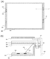
この課題についての詳細を、図7(A)、図7(B)に示す。図7(A)は、本件の従来技術に係る液晶表示装置100の構成の一例を示す図(上面図)である。また、図7(B)は、図7(A)のA−A’断面図である。 Details of this problem are shown in FIGS. 7A and 7B. FIG. 7A is a diagram (top view) showing an example of the configuration of a liquid crystal display device 100 according to the related art of the present case. Further, FIG. 7B is a cross-sectional view taken along the line A-A′ of FIG.
図7(B)では、波長変換部材106(代表的な例として量子ドットシート)が拡散部材105と光線制御部材107の間に設けられており、これらの部材は端部で光源保持部材103によって支持されている。液晶パネル101の有効表示領域下部の波長変換部材106では、主に光源109から発せられた一次光121の入射が支配的である。これに対して、波長変換部材106端部の領域では、拡散部材105と波長変換部材106の界面や反射部材104によって反射された二次光122の入射が支配的となる。上述したように、二次光122は均一ではないため、波長変換部材106の端部に入射する二次光122は、色ムラの発生要因となる。
In FIG. 7B, a wavelength conversion member 106 (a quantum dot sheet as a typical example) is provided between the
本発明は、波長変換部材を用いる光源装置において、色ムラの抑制を可能にする技術を提供することを目的とする。 An object of the present invention is to provide a technique capable of suppressing color unevenness in a light source device that uses a wavelength conversion member.
本発明の光源装置は、第1の光を発する光源と、端部に凸片を有し、前記第1の光が入射したことに応じて第2の光を発するシート状の変換部材と、前記凸片を支え、前記変換部材の外周領域を支持する支持部材と、前記支持部材と前記凸片との間に設けられ、前記変換部材の前記外周領域において前記第1の光の反射を抑制する抑制部材と、を備えることを特徴とする。 A light source device of the present invention includes a light source that emits first light, a sheet-shaped conversion member that has a convex piece at an end thereof, and emits second light in response to incidence of the first light, A support member that supports the convex piece and supports an outer peripheral area of the conversion member, and is provided between the support member and the convex piece, and suppresses reflection of the first light in the outer peripheral area of the conversion member. And a suppressing member that does.
本発明は、波長変換部材を用いる光源装置において、色ムラの抑制を可能にする。 The present invention makes it possible to suppress color unevenness in a light source device that uses a wavelength conversion member.
<実施例1>
以下、本発明の実施例1に係る光源装置について説明する。本実施例に係る光源装置は、例えば、光源装置からの光を透過することで画面に画像を表示する表示部を有する画像表示装置の光源装置として使用することができる。具体的には、本実施例に係る光源装置は、液晶表示装置、広告表示装置、標識表示装置、等の画像表示装置の光源装置として使用することができる。本実施例に係る光源装置は、液晶表示装置の液晶素子とは異なる表
示素子(例えば、MEMS(Micro Electro Mechanical System)シャッター)を用いた画像表示装置の光源装置として使用することもできる。また、本実施例に係る光源装置は、画像表示装置以外の装置(室内照明、街灯、など)の光源装置として使用することもできる。
<Example 1>
Hereinafter, the light source device according to the first embodiment of the present invention will be described. The light source device according to the present embodiment can be used, for example, as a light source device of an image display device having a display unit that displays an image on a screen by transmitting light from the light source device. Specifically, the light source device according to the present embodiment can be used as a light source device of an image display device such as a liquid crystal display device, an advertisement display device, and a sign display device. The light source device according to the present embodiment can also be used as a light source device for an image display device using a display element (for example, a MEMS (Micro Electro Mechanical System) shutter) different from the liquid crystal element of the liquid crystal display device. The light source device according to the present embodiment can also be used as a light source device for devices other than the image display device (indoor lighting, street lights, etc.).
図1は、本実施例に係る液晶表示装置100の断面図である。
液晶表示装置100は、液晶パネル101、液晶パネル保持部材102、光源装置を有する。光源装置は、光源保持部材103、反射部材104、拡散部材105、波長変換部材106、光線制御部材107、吸光部材108、光源109、基板110、等を有する。
FIG. 1 is a sectional view of a liquid crystal display device 100 according to this embodiment.
The liquid crystal display device 100 includes a
液晶パネル101は、光源装置からの光を透過することで画面に画像を表示する表示部である。液晶パネル101は複数の液晶素子を有しており、各液晶素子の透過率は不図示の画像出力装置から出力された画像データに応じて制御される。光源装置からの光が画像データに応じた透過率で液晶パネル101(各液晶素子)を透過することにより、画面に画像が表示される。図1の例では、液晶パネル101の光線制御部材107とは反対側の面が、画面に相当する。
The
液晶パネル保持部材102は、液晶パネル101を保持する。図1の例では、液晶パネル保持部材102によって、光線制御部材107と液晶パネル101との間隔が所定の間隔に保持される。
光源保持部材103は、光源109を保持する。図1の例では、光源保持部材103は、拡散部材105、波長変換部材106、光線制御部材107を支持する支持部材の役割を果たしている。なお、光源保持部材103は、光源109の熱を外部に放出する放熱構造を有していてもよい。
The liquid crystal
The light
反射部材104は、基板110の上面に設けられており、光源109から発せられた光を拡散部材105の側に反射する。図1の例では、反射部材104は板状の部材(反射板)である。なお、反射部材104は、光源保持部材103の側面に設けられていてもよい。それにより、そのような側面での反射効率を高めることができる。なお、反射部材104は、板状の部材でなくてもよい。例えば、反射部材103は、シート状の部材であってもよい。
The
拡散部材105は、光源109から発せられた光を拡散する。それにより、光源装置から発せられた光の輝度ムラや色ムラを低減することができる。拡散部材105としては、例えば、拡散板、拡散シート、集光シート、偏光シート、等を使用することができる。拡散部材105は、1つの部材によって構成されていてもよいし、複数の部材を重ねた構造を有していてもよい。なお、光源装置は、拡散部材105を有していなくてもよい。
The diffusing
波長変換部材106には、拡散部材105によって拡散された光が入射する。波長変換部材106は、光源109からの光によって励起が引き起こされることにより、光源が発する光の波長とは異なる波長の光を発生する。本実施例では、波長変換部材106は、R蛍光体とG蛍光体を有する。R蛍光体は、青色光によって励起が引き起こされることにより赤色光(赤色の光)を発生する蛍光体である。また、G蛍光体は青色光によって励起が引き起こされることにより緑色光(緑色の光)を発生する蛍光体である。本実施例では、蛍光体によって、当該蛍光体の励起を引き起こす励起光が、当該励起光よりも長波長側の光に変換される。そのため、蛍光体は、“光変換素子”や“波長変換素子”と呼ぶこともできる。本実施例では、波長変換部材106はR蛍光体として量子ドットを有し、また、G蛍光体として量子ドットを有する。また、本実施例では、光源装置から発せられる光として白色光が得られるように、R蛍光体とG蛍光体の数(割合)が調整されている。図1
の例では、波長変換部材106は、シート状の部材(量子ドットシート)である。なお、以下では、説明を簡単にするために、波長変換部材106の内部において、光の反射は生じないものとする。
なお、波長変換部材106の蛍光体は量子ドットでなくてもよい。たとえば、YAGなどの黄色蛍光体であってもよい。また、波長変換部材106はシート状の部材でなくてもよい。例えば、波長変換部材106はガラス管構造を有していてもよい。波長変換部材106は、入射した光の波長を変換し他の波長の光を発生することができる部材であればよく、その構造や形状は特に限定されない。なお、光源装置から発せられる光は、白色光に限らない。例えば、光源装置から発せられる光は、赤色光、緑色光、青色光、シアン色光、マゼンタ色光、イエロー色光、紫外光等であってもよい。また、励起によって発生する光は、赤色光と緑色光に限らない。例えば、励起によって発生する光は、青色光、シアン色光、マゼンタ色光、イエロー色光、等であってもよい。
また、波長変換部材106は、後述する光源109の側の面の端部において、光源保持部材103によって支持されている。
The light diffused by the diffusing
In the example, the
The phosphor of the
The
光線制御部材107は、波長変換部材106から発せられた光の指向性や偏光を制御する。それにより、光源装置から発せられた光の輝度や視野角を制御することができる。光線制御部材107としては、例えば、集光シート、偏光シート、等を使用することができる。光線制御部材107は、1つの部材によって構成されていてもよいし、複数の部材を重ねた構造を有していてもよい。また、本実施例に係る光源装置は、発光面から光を発するが、図1の例では光源装置の発光面130は、光線制御部材107の液晶パネル101の側の面である。なお、光源装置は、光線制御部材107を有していなくてもよい。
The light
吸光部材108は、光源保持部材103と波長変換部材106の間に設けられている。本実施例の場合、吸光部材108と波長変換部材106の間には、さらに拡散部材105が設けられている。吸光部材108は、光源109や拡散部材105、波長変換部材106、光線制御部材107、および液晶パネル101などからの光を吸収する部材である。それにより、色ムラの原因となる不要な光を吸収することができる。ここで、吸光部材108は、吸光シートや、あるいは、無反射シート、などを使用することができる。また、吸光部材108は、波長変換部材106を励起するための青色光のみを吸収する部材であってもよい。また、色ムラおよび輝度ムラの程度に応じて、吸光部材108を反射部材104よりも反射率が低い反射部材で構成することも可能である。
The
光源109には、本実施例では発光部材として青色光(青色の光)を発する発光ダイオード(LED)が使用される。また、本実施例では、光源109から発せられた光は、波長変換部材の励起光として使用される。なお、光源109が有する発光素子は、LEDに限らない。例えば、発光素子として、レーザー素子、有機EL素子、冷陰極管素子、プラズマ素子、等が使用されてもよい。なお、光源109から発せられる光は、青色光に限らない。例えば、光源109から発せられる光は、紫外光、等であってもよい。また、1つの光源109は、1つの発光素子を有していてもよいし、複数の発光素子を有していてもよい。
In this embodiment, the
本実施例の作用効果の具体例について説明する。上述したように光源109からは青色光が発せられる。光源109から発せられる色の光は、例えば、波長変換部材106で発生する第2、第3の色の光よりもスペクトルのピークの波長が短い光である。光源109から発せられる青色光のスペクトルは、例えば、440nm以上480nm以下の波長範囲にピーク(極大値)を有する。光源109から発せられる青色光のスペクトル(分光特性)の一例を図2(A)に示す。図2(A)の横軸は波長を示し、縦軸は強度を示す。本実施例では、光源109は、基板110の上面に配置される。光源109の配置数及び配置間隔は、光源装置から発せられる光の色、光源装置から発せられる光の輝度、光源装置
から発せられる光のムラ(輝度ムラや色ムラ)、等を考慮して決定される。
A specific example of the operation and effect of this embodiment will be described. As described above, the
波長変換部材106は、光源109から発せられた青色光の一部を緑色光及び赤色光に変換し、青色光と赤色光と緑色光を発することになる。波長変換部材106で発生する赤色光のスペクトルは、例えば、580nm以上700nm以下の波長範囲にピークを有する。また、波長変換部材106で発生する緑色光のスペクトルは、例えば、500nm以上550nm以下の波長範囲にピークを有する。波長変換部材106から発せられる合成光のスペクトルの一例を図2(B)に示す。図2(B)から、波長変換部材106から発せられる合成光のスペクトルが、青色光のスペクトルのピーク、赤色光のスペクトルのピーク、及び、緑色光のスペクトルのピーク、の3つのピークを有することがわかる。図2に示すスペクトルを有する合成光は、例えば、白色光である。
なお、光源109から発せられる光が紫外光である場合、紫外光を励起光として波長変換部材106で波長変換された青色光、緑色光、赤色光の合成光を得ることができる。合成光は、光源や波長変換部材106によっても変わるが、例えば白色光である。
The
When the light emitted from the
波長変換部材106の端部に入射する光は、二次光122が支配的となる。例えば、波長変換部材106に量子ドットシートが使用される場合、二次光122は光の量が不均一であるため、波長変換部材106の端部では量子ドットにあたる光の量が局所的にばらつき、出射光に色ムラが生じる。
The
本実施例では、上記の課題を解決する方法として、図1に示すように波長変換部材106の光源109側の面と光源保持部材103との間に吸光部材108を設けることを特徴とする。これにより、二次光122は吸光部材108によって吸収され、波長変換部材106端部への二次光122の入射が抑制され、色ムラの発生も抑制されることになる。
In the present embodiment, as a method for solving the above-mentioned problems, as shown in FIG. 1, a
以上述べたように、本実施例によれば、波長変換部材106の光源109側の面と光源保持部材103との間に吸光部材108を設ける、という簡易な構成で、光源装置の端部における色ムラや輝度ムラを抑制することができる。
As described above, according to the present embodiment, the
<実施例2>
以下、本発明の実施例2に係る光源装置について説明する。本実施例では、波長変換部材などのシート部材の面内の位置を保持するために、光源保持部材の端部に凹凸を設けた場合の構成について説明する。
図3(A)は、本実施例に係る液晶表示装置200の構成の一例を示す図(上面図)である。また、図3(B)は、図3(A)のA−A’断面図である。また、図3(A)のB−B’断面は、図1と同様である。
液晶表示装置200は、液晶パネル201、液晶パネル保持部材202、光源装置、等を有する。光源装置は、光源保持部材203、反射部材204、拡散部材205、波長変換部材206、光線制御部材207、吸光部材208、光源209、基板210、シート固定部材211等を有する。
液晶パネル201は、実施例1(図1)の液晶パネル101と同じ部材である。
液晶パネル保持部材202は、実施例1の液晶パネル保持部材102と同じ部材である。
光源保持部材203は、実施例1の光源保持部材103と同じ材質である。なお、実施例1と同様に、光源保持部材203は、拡散部材205、波長変換部材206、光線制御部材207を支持する支持部材の役割を果たしている。
反射部材204は、実施例1の反射部材104と同じ材質である。
拡散部材205は、実施例1の拡散部材105と同じ材質である。
波長変換部材206は、実施例1の波長変換部材106と同じ材質である。
光線制御部材207は、実施例1の光線制御部材107と同じ材質である。
吸光部材208は、実施例1の吸光部材108と同じ材質である。
光源209は、実施例1の光源109と同じ部材である。
基板210は、実施例1の基板110と同じ部材である。
<Example 2>
Hereinafter, the light source device according to the second embodiment of the present invention will be described. In the present embodiment, a configuration will be described in which unevenness is provided at the end of the light source holding member in order to hold the in-plane position of the sheet member such as the wavelength conversion member.
FIG. 3A is a diagram (top view) showing an example of the configuration of the liquid
The liquid
The
The liquid crystal
The light
The
The diffusing
The
The light
The
The
The
本実施例では、図3(A)に示すように、光源保持部材203が端部に凹凸の形状を有する。また、拡散部材205、波長変換部材206や光線制御部材207などのシート部材や反射部材204も端部に凹凸の形状を有する。各シート部材は、凹部が光源保持部材203の凸部280に合うように設けられる。この構造により、各シート部材は位置を合わせて設けられ、面内での位置ずれが防止される。
In this embodiment, as shown in FIG. 3A, the light
また、図3(A)の断面、すなわち図1に示す断面図においては、光源保持部材203が波長変換部材206の光源209の側の面の端部において、波長変換部材206を支持している。なお、本実施例では波長変換部材206と一緒に拡散部材205と光線制御部材207も光源保持部材203によって支持されている。
Further, in the cross section of FIG. 3A, that is, the cross sectional view shown in FIG. 1, the light
実施例1と同様に、本実施例においても波長変換部材の端部に入射する二次光122が課題となる。特に本実施例では、光源保持部材203端部の凹凸による、A−A’断面とB−B’断面における端部の構造の違いが問題となる。このような構造の違いが端部における光の反射の違いを生む。より具体的には、光が波長変換部材206を通過する回数に違いが生じ、これが色ムラの発生要因となる。この課題を解決するため、凹凸部の影響をなくすように液晶パネル201の有効表示領域に対して十分広い大きさの量子ドットシート面積とすることも考えられるが、製品の額縁が大きくなってしまい商品性が損なわれる可能性がある。
Similar to the first embodiment, the
この課題を解決するため、本実施例では、図3(A)に示すように、波長変換部材206等のシート部材は端部に凸部(以下、光源保持部材の凸部と区別するために凸片250と呼ぶ)を有する。さらに断面方向の位置関係を説明すると、凸片250の領域において、図1に示すように、波長変換部材206の光源209の側の面と光源保持部材203との間に吸光部材208が設けられている。なお、吸光部材208の形状と大きさは、凸片250と同一でなくてもよい。凸片250以外の領域では、図3(B)から分かるように二次光の問題が起きにくいので、吸光部材は設けなくてもよい。
In order to solve this problem, in this embodiment, as shown in FIG. 3A, the sheet member such as the
このような構造とすることで、凸片250の領域における波長変換部材206での二次光122の波長変換が抑制され、また端部の反射構造が均一になる。これによって波長変換部材206から出射される光の色ムラが抑制されることになる。
With such a structure, the wavelength conversion of the
また、光源保持部材203が端部に凹凸を有するため、波長変換部材206等のシート部材が有する凹凸部と位置を合わせることができ、またこれによって面内の位置ずれを防止することができる。
Further, since the light
<実施例3>
本実施例では、光源保持部材103に対して拡散部材105等を固定するために固定部材を用いる場合の光源装置の構成について説明する。
図4(A)は、本実施例に係る液晶表示装置300の構成の一例を示す図(上面図)である。また、図4(B)は、図4(A)のC−C’断面図である。
<Example 3>
In the present embodiment, a configuration of a light source device in which a fixing member is used to fix the
FIG. 4A is a diagram (top view) showing an example of the configuration of the liquid
液晶表示装置300は、液晶パネル301、液晶パネル保持部材302、光源装置、等を有する。光源装置は、光源保持部材203、反射部材204、拡散部材205、波長変換部材306、光線制御部材307、吸光部材308、光源309、基板310、シート固定部材311等を有する。
液晶パネル301は、実施例1(図1)の液晶パネル101と同じ部材である。
液晶パネル保持部材302は、実施例1の液晶パネル保持部材102と同じ部材である。
光源保持部材303は、実施例1の光源保持部材103と同じ材質である。なお、実施例1と同様に、光源保持部材303は、拡散部材305、波長変換部材306、光線制御部材307を支持する支持部材の役割を果たしている。
反射部材304は、実施例1の反射部材104と同じ材質である。
拡散部材305は、実施例1の拡散部材105と同じ材質である。
波長変換部材306は、実施例1の波長変換部材106と同じ材質である。
光線制御部材307は、実施例1の光線制御部材107と同じ材質である。
吸光部材308は、実施例1の吸光部材108と同じ材質である。
光源309は、実施例1の光源109と同じ材質である。
基板310は、実施例1の基板110と同じ部材である。
シート固定部材311は、拡散部材305、波長変換部材306、および光線制御部材307などを光源保持部材303に対して固定するための部材である。シート固定部材311はピン構造であってもよいし、リベット構造であってもよく、上述のシート部材を固定する任意の構造をとることができる。また、素材は金属であってもよいし、プラスチックなどの樹脂であってもよい。
The liquid
The
The liquid crystal
The light
The reflecting
The diffusing
The
The light
The
The
The
The
図4(A)と図4(B)に示すように、本実施例では実施例2と同様に、凸片350の領域に、波長変換部材306の光源309の側の面と光源保持部材303との間に吸光部材308が設けられている。なお、吸光部材308の面積や形状は、凸片350と同一でなくともよい。
As shown in FIGS. 4A and 4B, in this embodiment, in the same manner as in the second embodiment, the surface of the
本実施例は、図4(A)と図4(B)に示すように凸片350において、拡散部材305、波長変換部材306、および光線制御部材307などのシート部材をシート固定部材311によって、光源保持部材303に対して固定することを特徴とする。
本実施例のような構成においても、凸片350の領域における波長変換部材306での二次光322の波長変換が抑制される。これによって波長変換部材306から出射される光の色ムラが抑制されることになる。
さらに、シート固定部材311を用いることによって、波長変換部材306などのシート部材が、実施例1の場合に比べてより強固に光源保持部材303に固定されることになる。この結果、液晶表示装置300が回転する場合、例えば図4(A)の状態から90度回転する場合においても、波長変換部材306などのシート部材が所望の位置に固定される。また、シート部材の保持の役割はシート固定部材311が担うため、凸片の面積は実施例2の場合に比べて小さくすることができ、製造コストの削減にもつながる。
In this embodiment, as shown in FIGS. 4A and 4B, in the
Also in the configuration as in the present embodiment, the wavelength conversion of the
Furthermore, by using the
<実施例4>
以下、本発明の実施例4に係る光源装置について説明する。本実施例では、光源が千鳥配置や三角形配置など、面内に規則的に配置される場合を想定している。ところで一般的に、波長変換部材や拡散部材、光線制御部材などのシート部材は、液晶パネルの有効表示領域を確実に覆うために、有効表示領域以上の面積を有する。このような構成では、光源との距離によって、上辺下辺側と左辺右辺側で光が届く領域に違いが生じる。本実施例では、この違いを考慮した色ムラの抑制方法について説明する。
<Example 4>
Hereinafter, the light source device according to the fourth embodiment of the present invention will be described. In this embodiment, it is assumed that the light sources are regularly arranged in a plane such as a staggered arrangement or a triangular arrangement. By the way, generally, a sheet member such as a wavelength converting member, a diffusing member, or a light beam controlling member has an area larger than the effective display area in order to surely cover the effective display area of the liquid crystal panel. In such a configuration, there is a difference in the area where the light reaches on the lower side of the upper side and the right side of the left side depending on the distance from the light source. In this embodiment, a method for suppressing color unevenness in consideration of this difference will be described.
図5は、本実施例に係る光源装置400の構成の一例を示す図(拡散部材から光源側を見たときの上面図)である。
光源装置は、反射部材404、拡散部材(図示しない)、波長変換部材(図示しない)、光線制御部材(図示しない)、第一吸光部材408、光源409、基板(図示しない)、第二吸光部材412等を有する。
反射部材404は、実施例1の反射部材104と同じ材質である。
第一吸光部材408は、実施例1の吸光部材108と同じ材質である。本実施例では、第一吸光部材408は液晶表示パネルの有効表示領域外側の左辺右辺に設けられた吸光部材である。
光源409は、実施例1の光源109と同じ部材である。
第二吸光部材412は、実施例1の吸光部材108と同じ材質である。本実施例では、第二吸光部材412は、液晶表示パネルの有効表示領域外側の上辺下辺に設けられた吸光部材である。
FIG. 5 is a diagram showing an example of the configuration of the
The light source device includes a
The
The first
The
The second
本実施例では、第一吸光部材408と光源409との距離をL1とする。また、第二吸光部材412と光源409との距離をL2とする。
さらに、L1とL2の関係は、
L1>L2
とする。
In this embodiment, the distance between the first
Furthermore, the relationship between L1 and L2 is
L1>L2
And
実施例4では、波長変換部材に平行な方向であって光源から遠ざかる方向の第二吸光部材412の長さ(以下「吸光幅」と呼ぶ)を、L1とL2の関係性に応じて変更することを特徴とする。
具体的には、第一吸光部材408の大きさを波長変換部材406と光源保持部材の接触面積と同一とした上で、第二吸光部材412の吸光幅は第一吸光部材408とより小さくなるようにする。このような構造とする理由について説明する。まず、第一吸光部材308の面積は、波長変換部材406と光源保持部材の接触面積と同一とすることで、左辺右辺側の波長変換部材の端部における波長変換は抑制される。これに対し、L1とL2の大きさが異なる場合、第二吸光部材の吸光幅はL1とL2の関係に応じて小さくしても構わない。
液晶パネルの有効表示領域外側の波長変換部材において、光が届く領域は光源409との距離によって変化する。このことを説明するため、端部に入射する光の角度を考える。図1に示すように、入射光(この場合は二次光122)の入射角は、入射面(この場合は波長変換部材106)に垂直な線からの角度として定義される。波長変換部材などのシート部材の端部と光源409との距離が大きい場合、端部への入射光の入射角度は大きくなり、入射光は光源409から遠ざかる方向により遠くまで届くことになる。反対に、波長変換部材などのシート部材の端部と光源409との距離が小さい場合、端部への入射光の入射角度は小さくなり、入射光が届く距離はより小さくなる。したがって、本実施例のように上辺下辺側の端部と左辺右辺側の端部で光源との距離が異なる場合、各端部において入射光が届く距離が異なり、色ムラが生じる原因となる領域に相違が生じる。そこで本実施例では、L1、L2の距離に応じて第二吸光部材412の吸光幅を変化させ、上辺下辺側と左辺右辺側の端部における波長変換が均一に行われるようにしている。
In the fourth embodiment, the length of the second
Specifically, the size of the first
In the wavelength conversion member outside the effective display area of the liquid crystal panel, the area where the light reaches changes depending on the distance from the
具体的には、本実施例の場合、
L1>L2
の関係であるため、上辺下辺側の入射光は、左辺右辺側の入射光よりも入射角度が小さくなる。したがって、波長変換部材の上辺下辺側の端部には、左辺右辺側の端部よりも光が伝搬しにくくなるため、上辺下辺側に設ける第二吸光部材412の吸光幅を第一吸光部材412よりも小さくすることができる。
Specifically, in the case of this embodiment,
L1>L2
Therefore, the incident light on the lower side of the upper side has a smaller incident angle than the incident light on the right side of the left side. Therefore, since light is less likely to propagate to the end on the lower side of the upper side of the wavelength conversion member than the end on the right side of the left side, the absorption width of the second
以上述べたように、本実施例によれば、光源409が面内で規則的な配置となっており、かつ光源409と波長変換部材の端部の距離が上辺下辺側と左辺右辺側で異なる場合において、端部での波長変換が抑制される。これによって、各辺における波長変換が均一になされ、光源装置の色ムラや輝度ムラを抑制することができる。また、本実施例では、吸光幅を小さくすることにより、第二吸光部材412の面積を縮小できるため、光源装置4
00の製造コストを低減することができる。
As described above, according to this embodiment, the
The manufacturing cost of 00 can be reduced.
<実施例5>
以下、本発明の実施例5に係る光源装置について説明する。本実施例では、光源を直下型導光板側面に配置した構造の場合について説明する。
図6は、本実施例に係る液晶表示装置500の構成の一例を示す図(断面図)である。液晶表示装置500は、液晶パネル501、液晶パネル保持部材502、光源装置、等を有する。光源装置は、光源保持部材503、反射部材504、導光部材505、波長変換部材506、光線制御部材507、第一吸光部材508、光源509、基板510、遮光部材511、および第二吸光部材512等を有する。
<Example 5>
Hereinafter, the light source device according to the fifth embodiment of the present invention will be described. In this embodiment, the case where the light source is arranged on the side surface of the direct type light guide plate will be described.
FIG. 6 is a diagram (cross-sectional view) showing an example of the configuration of the liquid
液晶パネル501は、実施例1(図1)の液晶パネル101と同じ部材である。
液晶パネル保持部材502は、実施例1の液晶パネル保持部材102と同じ材質である。
光源保持部材503は、実施例1の光源保持部材103と同じ材質である。また、光源保持部材503は、波長変換部材506の光源509の側の面の端部において、波長変換部材506を支持する支持部材としての役割を果たしている。
反射部材504は、実施例1の反射部材104と同じ部材である。光源509から発する光を、後述する導光部材505の方に反射するように設けてある。また、本実施例では、波長変換部材506の光源509の側の面の端部において、波長変換部材506を支持する支持部材としての役割を果たしている。
導光部材505は、入射面、および出射面を有する。入射面は、光源509から発せられた光が入射する入射面であり、出射面は入射面に入射した光を出射する面である。図6の例では、入射面は、導光部材505の側面のうち、光源509が存在する側面である。導光部材505の出射面は、波長変換部材506側の面である。図6の例では、導光部材505として、板状の部材(導光板)が使用されている。なお、導光部材505は、板状の部材でなくてもよい。
The
The liquid crystal
The light
The reflecting
The
波長変換部材506は、実施例1の波長変換部材106と同じ材質である。
光線制御部材507は、実施例1の光線制御部材107と同じ材質である。
第一吸光部材508は、実施例1の吸光部材108と同じ材質である。光源保持部材503の光源509から遠い方の壁面側に設けられている。
光源509は、実施例1の光源109と同じ材質である。
基板510は、実施例1の基板110と同じ材質である。
遮光部材511は、光源509から発せられた光が導光部材505を介さずに直接液晶パネル501方向へ放射されることを防ぐための部材である。なお、本遮光部材は、輝度ムラ、色ムラ性能の観点から反射部材であってもよい。
第二吸光部材512は、実施例1の吸光部材108と同じ部材である。光源保持部材503の光源509に近い方の壁面側に設けられている。
本実施例では、第一吸光部材508は、波長変換部材506の側の面と光源保持部材503との間に設けられ、第二吸光部材512は、波長変換部材506の側の面と反射部材504との間に設けられている。また、第一吸光部材508の大きさは、たとえば波長変換部材506と光源保持部材503の接触面積と同一とし、第二吸光部材512の大きさは第一吸光部材508よりも小さい、もしくは削除することとする。
The
The light
The first
The
The
The
The second
In this embodiment, the first
このような構造とする理由について説明する。図6において、光源509から遠い端部にある、波長変換部材506の光源509側の領域への入射光520の入射角をθとする。一方、光源509に近い端部にある、波長変換部材506の光源509側の領域への入射光521の入射角をθ’とする。θはθ’より大きく、入射光520が届く距離も大きいため、それに応じて第一吸光部材508の吸光幅を十分大きくとる必要がある。一方、
入射光521が届く距離は入射光520に比べて小さく、第二吸光部材512の吸光幅は、第一吸光部材よりも小さくすることができる。または、遮光部材511によって光の伝搬を完全に防ぐ構造となっている場合には、第二吸光部材512を設ける必要が無い。
The reason for having such a structure will be described. In FIG. 6, it is assumed that the incident angle of the incident light 520 to the region on the
The distance traveled by the
このような構造とすることで、光源509に近い端部と遠い端部において、光が届く距離に応じて、波長変換を抑制することができる。この結果、波長変換が面内で均一化され、波長変換部材506から出射される光の色も均一化されることになる。
With such a structure, wavelength conversion can be suppressed at the end near the
以上述べたように、本実施例によれば、光源509から遠い端部に設けられる第一吸光部材508と、光源509に近い端部に設けられる第二吸光部材512の吸光幅を変更する、という構成により、光源装置の色ムラや輝度ムラを抑制することができる。また、本実施例では、第二吸光部材512の面積を縮小できるため、光源装置の製造コストを低減することができる。なお、図示しないが、本実施例の構成においても、実施例2,3のように端部にシート部材を保持するための保持構造を有していてもよい。
As described above, according to the present embodiment, the light absorption widths of the first
なお、実施例1〜5はあくまで一例であり、本発明の要旨の範囲内で実施例1〜5の構成を適宜変形したり変更したりすることにより得られる構成も、本発明に含まれる。実施例1〜4の構成を適宜組み合わせて得られる構成も、本発明に含まれる。 The first to fifth embodiments are merely examples, and the present invention includes configurations obtained by appropriately modifying or changing the configurations of the first to fifth embodiments within the scope of the present invention. The present invention also includes configurations obtained by appropriately combining the configurations of Examples 1 to 4.
103,203,303,503 光源保持部材
106,206,306,506 波長変換部材
108,208,308 吸光部材
109,209,309,409,509 光源
408,508 第一吸光部材
412,512 第二吸光部材
103,203,303,503 Light source holding member 106,206,306,506 Wavelength conversion member 108,208,308 Light absorbing member 109,209,309,409,509 Light source 408,508 First light absorbing member 412,512 Second light absorbing Element
Claims (15)
端部に凸片を有し、前記第1の光が入射したことに応じて第2の光を発するシート状の変換部材と、
前記凸片を支え、前記変換部材の外周領域を支持する支持部材と、
前記支持部材と前記凸片との間に設けられ、前記変換部材の前記外周領域において前記第1の光の反射を抑制する抑制部材と、
を備えることを特徴とする光源装置。 A light source that emits a first light,
A sheet-shaped conversion member which has a convex piece at an end portion thereof and emits second light in response to the incidence of the first light;
A support member that supports the convex piece and supports the outer peripheral region of the conversion member,
A suppression member which is provided between the support member and the convex piece, and which suppresses reflection of the first light in the outer peripheral region of the conversion member,
A light source device comprising:
前記支持部材内に設けられ、光を反射する反射部材をさらに備え、
前記抑制部材は、前記変換部材の前記外周領域と前記支持部材との間に設けられ、前記第1の光に対する反射率が前記反射部材よりも低い部材であることを特徴とする請求項1に記載の光源装置。 The support member is a box-shaped housing that houses the light source,
Further comprising a reflection member provided in the support member and reflecting light,
The suppression member is provided between the outer peripheral region of the conversion member and the support member, and has a reflectance with respect to the first light lower than that of the reflection member. The light source device described.
を備える請求項1から請求項3の何れか1項に記載の光源装置。 The light source device according to claim 1 , further comprising a fixing member that fixes the conversion member and the suppressing member to the support member.
前記第1の端部と前記光源との距離が前記第2の端部と前記光源との距離より大きい場合に、前記変換部材と平行な方向であって前記光源から遠ざかる方向における前記第2の抑制部材の幅が、前記方向における前記第1の抑制部材の幅よりも短い
ことを特徴とする請求項1から請求項4の何れか1項に記載の光源装置。 The suppressing member includes a first suppressing member provided at a first end portion of the conversion member and a second suppressing member provided at a second end portion of the conversion member,
When the distance between the first end and the light source is larger than the distance between the second end and the light source, the second direction in a direction parallel to the conversion member and away from the light source. The light source device according to any one of claims 1 to 4 , wherein the width of the suppressing member is shorter than the width of the first suppressing member in the direction.
ことを特徴とする請求項1から請求項5の何れか1項に記載の光源装置。 The light source device according to any one of claims 1 to 5 , wherein the suppressing member is a member that absorbs at least the first light.
ことを特徴とする請求項1から請求項6の何れか1項に記載の光源装置。 Said conversion member, the light source device according to any one of claims 1 to 6, characterized in that it comprises a phosphor.
ことを特徴とする請求項1から請求項7の何れか1項に記載の光源装置。 The said conversion member has a quantum dot, The light source device in any one of Claim 1 to 7 characterized by the above-mentioned.
ことを特徴とする請求項1から請求項8の何れか1項に記載の光源装置。 The light source device according to any one of claims 1 to 8 , wherein the first light is light having a spectrum peak wavelength shorter than that of the second light.
ことを特徴とする請求項1から請求項9の何れか1項に記載の光源装置。 The conversion member converts blue light into green light and red light, and emits the blue light, the green light, and the red light, according to any one of claims 1 to 9 . Light source device.
ことを特徴とする請求項1から請求項9の何れか1項に記載の光源装置。 Said conversion member, the ultraviolet light is converted into blue light, green light and red light, the blue light, any one of claims 1 to 9, characterized in that to emit the green light and the red light The light source device according to.
前記赤色光のスペクトルは、580nm以上700nm以下の波長範囲にピークを有し、
前記緑色光のスペクトルは、500nm以上550nm以下の波長範囲にピークを有する
ことを特徴とする請求項10または請求項11に記載の光源装置。 The spectrum of the blue light has a peak in a wavelength range of 440 nm or more and 480 nm or less,
The spectrum of the red light has a peak in a wavelength range of 580 nm or more and 700 nm or less,
The spectrum of the green light source device according to claim 10 or claim 11 characterized in that it has a peak in 550nm or less in the wavelength range of 500 nm.
前記第1の光が入射したことに応じて第2の光を発するシート状の変換部材と、A sheet-shaped conversion member that emits second light in response to the incidence of the first light;
前記変換部材の外周領域を支持する支持部材と、A support member supporting the outer peripheral region of the conversion member,
前記変換部材の前記外周領域において前記第1の光の反射を抑制する抑制部材と、A suppression member for suppressing reflection of the first light in the outer peripheral region of the conversion member,
を備え、Equipped with
前記抑制部材は、前記変換部材の第1の端部に設けられる第1の抑制部材と、前記変換部材の第2の端部に設けられる第2の抑制部材と、を有し、The suppressing member includes a first suppressing member provided at a first end portion of the conversion member and a second suppressing member provided at a second end portion of the conversion member,
前記第1の端部と前記光源との距離が前記第2の端部と前記光源との距離より大きい場合に、前記変換部材と平行な方向であって前記光源から遠ざかる方向における前記第2の抑制部材の幅が、前記方向における前記第1の抑制部材の幅よりも短いWhen the distance between the first end portion and the light source is larger than the distance between the second end portion and the light source, the second portion in a direction parallel to the conversion member and away from the light source. The width of the suppressing member is shorter than the width of the first suppressing member in the direction.
ことを特徴とする光源装置。A light source device characterized by the above.
前記光源装置から出力された光を透過して画像を表示する表示パネルと、
を備える表示装置。 A light source device according to any one of claims 1 to 13,
A display panel that displays an image by transmitting the light output from the light source device;
A display device including.
Priority Applications (5)
| Application Number | Priority Date | Filing Date | Title |
|---|---|---|---|
| JP2016001178A JP6700792B2 (en) | 2016-01-06 | 2016-01-06 | Light source |
| EP16204216.2A EP3190457A1 (en) | 2016-01-06 | 2016-12-15 | Light source device comprising wavelength conversion member |
| US15/394,926 US10151950B2 (en) | 2016-01-06 | 2016-12-30 | Light source device with color conversion member, supporting member and light suppressing member |
| KR1020170000032A KR20170082458A (en) | 2016-01-06 | 2017-01-02 | Light source device |
| CN201710011144.0A CN106990608A (en) | 2016-01-06 | 2017-01-06 | Light supply apparatus |
Applications Claiming Priority (1)
| Application Number | Priority Date | Filing Date | Title |
|---|---|---|---|
| JP2016001178A JP6700792B2 (en) | 2016-01-06 | 2016-01-06 | Light source |
Publications (3)
| Publication Number | Publication Date |
|---|---|
| JP2017123250A JP2017123250A (en) | 2017-07-13 |
| JP2017123250A5 JP2017123250A5 (en) | 2019-01-31 |
| JP6700792B2 true JP6700792B2 (en) | 2020-05-27 |
Family
ID=57794037
Family Applications (1)
| Application Number | Title | Priority Date | Filing Date |
|---|---|---|---|
| JP2016001178A Expired - Fee Related JP6700792B2 (en) | 2016-01-06 | 2016-01-06 | Light source |
Country Status (5)
| Country | Link |
|---|---|
| US (1) | US10151950B2 (en) |
| EP (1) | EP3190457A1 (en) |
| JP (1) | JP6700792B2 (en) |
| KR (1) | KR20170082458A (en) |
| CN (1) | CN106990608A (en) |
Families Citing this family (6)
| Publication number | Priority date | Publication date | Assignee | Title |
|---|---|---|---|---|
| US10465861B1 (en) * | 2016-01-13 | 2019-11-05 | OPē, LLC | Light source with quantum dot layer |
| KR102343413B1 (en) * | 2017-07-19 | 2021-12-24 | 삼성디스플레이 주식회사 | Display device and manufacturing method thereof |
| US10642091B2 (en) * | 2018-02-05 | 2020-05-05 | Radiant Choice Limited | Displays |
| CN109521604A (en) * | 2018-12-21 | 2019-03-26 | 厦门天马微电子有限公司 | A kind of backlight module and display device |
| JP6866903B2 (en) * | 2019-03-05 | 2021-04-28 | 日亜化学工業株式会社 | Luminous module |
| WO2023141961A1 (en) * | 2022-01-28 | 2023-08-03 | Huawei Technologies Co., Ltd. | Display device for eye care |
Family Cites Families (16)
| Publication number | Priority date | Publication date | Assignee | Title |
|---|---|---|---|---|
| TWM289865U (en) * | 2005-11-08 | 2006-04-21 | Lighthouse Technology Co Ltd | Sectional light emitting diode backlight unit |
| JP2011171365A (en) | 2010-02-16 | 2011-09-01 | Panasonic Corp | Semiconductor light emitting module, light source device and liquid crystal display device |
| JP2012022028A (en) | 2010-07-12 | 2012-02-02 | Ns Materials Kk | Liquid crystal display |
| JP5737011B2 (en) * | 2011-01-18 | 2015-06-17 | 日本電気硝子株式会社 | LIGHT EMITTING DEVICE, LIGHT EMITTING DEVICE CELL, AND LIGHT EMITTING DEVICE MANUFACTURING METHOD |
| JP6121915B2 (en) * | 2011-03-07 | 2017-04-26 | コーニンクレッカ フィリップス エヌ ヴェKoninklijke Philips N.V. | Light emitting module, lamp, lighting fixture, and display device |
| JP6192897B2 (en) * | 2012-04-11 | 2017-09-06 | サターン ライセンシング エルエルシーSaturn Licensing LLC | LIGHT EMITTING DEVICE, DISPLAY DEVICE, AND LIGHTING DEVICE |
| JP2014170218A (en) | 2013-02-05 | 2014-09-18 | Canon Inc | Image display device and method for controlling the same |
| JP6217187B2 (en) * | 2013-07-03 | 2017-10-25 | ソニー株式会社 | Light emitting device and display device |
| US9857524B2 (en) * | 2013-11-20 | 2018-01-02 | Huawei Device (Dongguan) Co., Ltd. | Liquid crystal module and electronic device |
| JP2015111518A (en) * | 2013-12-06 | 2015-06-18 | 株式会社ジャパンディスプレイ | Backlight and liquid crystal display device using the same |
| KR102126176B1 (en) * | 2014-02-05 | 2020-06-25 | 삼성디스플레이 주식회사 | Wavelengh conversion member, and method for manufacturing the same, and backlight assembly including the same |
| JP6021967B2 (en) * | 2014-04-21 | 2016-11-09 | キヤノン株式会社 | Light source device and image display device |
| US9535206B2 (en) * | 2014-06-09 | 2017-01-03 | Apple Inc. | Display with structures for reducing blue edge effects |
| JP2016035908A (en) | 2014-08-01 | 2016-03-17 | キヤノン株式会社 | Light source device |
| KR101510855B1 (en) * | 2014-08-22 | 2015-04-09 | 삼성전자 주식회사 | Mold frames and optical sheets and backlight units and liquid crystal displays including the same |
| EP3279548B1 (en) * | 2015-04-01 | 2020-07-15 | Sharp Kabushiki Kaisha | Lighting device, display device, and television receiving device |
-
2016
- 2016-01-06 JP JP2016001178A patent/JP6700792B2/en not_active Expired - Fee Related
- 2016-12-15 EP EP16204216.2A patent/EP3190457A1/en not_active Withdrawn
- 2016-12-30 US US15/394,926 patent/US10151950B2/en not_active Expired - Fee Related
-
2017
- 2017-01-02 KR KR1020170000032A patent/KR20170082458A/en unknown
- 2017-01-06 CN CN201710011144.0A patent/CN106990608A/en active Pending
Also Published As
| Publication number | Publication date |
|---|---|
| CN106990608A (en) | 2017-07-28 |
| EP3190457A1 (en) | 2017-07-12 |
| JP2017123250A (en) | 2017-07-13 |
| KR20170082458A (en) | 2017-07-14 |
| US10151950B2 (en) | 2018-12-11 |
| US20170192304A1 (en) | 2017-07-06 |
Similar Documents
| Publication | Publication Date | Title |
|---|---|---|
| JP6700792B2 (en) | Light source | |
| US10061188B2 (en) | Illumination system and projection apparatus having reflection cover | |
| JP6021967B2 (en) | Light source device and image display device | |
| CN114730044A (en) | Directional lighting device and privacy display | |
| JP5026620B2 (en) | Surface light source and liquid crystal display device | |
| WO2017002308A1 (en) | Backlight device and liquid crystal display device | |
| TWI486648B (en) | Surface light source device and liquid crystal display device | |
| WO2012153514A1 (en) | Illumination device and liquid crystal display device | |
| JP2012155999A (en) | Lighting system and image display device | |
| JP2007025285A (en) | Back light for liquid crystal | |
| JP2009244861A (en) | Image display apparatus | |
| TWI567456B (en) | Surface light source device and liquid crystal display device | |
| EP3699488B1 (en) | Display device | |
| WO2016121530A1 (en) | Lighting device and display device | |
| JP2012238462A (en) | Light mixing unit, planar light source device and liquid crystal display device | |
| TWI405102B (en) | Backlight module and optical touch panel | |
| JP5208039B2 (en) | Display device and light source device | |
| JP4125756B2 (en) | Flat panel display backlight module | |
| JP2007080520A (en) | Backlight device | |
| JP2017162726A (en) | Lighting device and display device | |
| WO2018123812A1 (en) | Illuminating device and display device | |
| JP4429870B2 (en) | Liquid crystal display | |
| WO2020196572A1 (en) | Planar light source device, and display device | |
| WO2014192659A1 (en) | Light-source device and display device | |
| JP2018037172A (en) | Backlight device, display device and television receiver |
Legal Events
| Date | Code | Title | Description |
|---|---|---|---|
| RD02 | Notification of acceptance of power of attorney |
Free format text: JAPANESE INTERMEDIATE CODE: A7422 Effective date: 20181116 |
|
| A521 | Request for written amendment filed |
Free format text: JAPANESE INTERMEDIATE CODE: A523 Effective date: 20181213 |
|
| A621 | Written request for application examination |
Free format text: JAPANESE INTERMEDIATE CODE: A621 Effective date: 20181213 |
|
| A977 | Report on retrieval |
Free format text: JAPANESE INTERMEDIATE CODE: A971007 Effective date: 20190814 |
|
| A131 | Notification of reasons for refusal |
Free format text: JAPANESE INTERMEDIATE CODE: A131 Effective date: 20190910 |
|
| A521 | Request for written amendment filed |
Free format text: JAPANESE INTERMEDIATE CODE: A523 Effective date: 20191009 |
|
| TRDD | Decision of grant or rejection written | ||
| A01 | Written decision to grant a patent or to grant a registration (utility model) |
Free format text: JAPANESE INTERMEDIATE CODE: A01 Effective date: 20200310 |
|
| A61 | First payment of annual fees (during grant procedure) |
Free format text: JAPANESE INTERMEDIATE CODE: A61 Effective date: 20200501 |
|
| R151 | Written notification of patent or utility model registration |
Ref document number: 6700792 Country of ref document: JP Free format text: JAPANESE INTERMEDIATE CODE: R151 |
|
| LAPS | Cancellation because of no payment of annual fees |