EP3695320B1 - Pcie mit niedriger leistung - Google Patents
Pcie mit niedriger leistung Download PDFInfo
- Publication number
- EP3695320B1 EP3695320B1 EP18795894.7A EP18795894A EP3695320B1 EP 3695320 B1 EP3695320 B1 EP 3695320B1 EP 18795894 A EP18795894 A EP 18795894A EP 3695320 B1 EP3695320 B1 EP 3695320B1
- Authority
- EP
- European Patent Office
- Prior art keywords
- signaling
- pcie
- differential
- ended
- phy
- Prior art date
- Legal status (The legal status is an assumption and is not a legal conclusion. Google has not performed a legal analysis and makes no representation as to the accuracy of the status listed.)
- Active
Links
Images


Classifications
-
- G—PHYSICS
- G06—COMPUTING OR CALCULATING; COUNTING
- G06F—ELECTRIC DIGITAL DATA PROCESSING
- G06F1/00—Details not covered by groups G06F3/00 - G06F13/00 and G06F21/00
- G06F1/26—Power supply means, e.g. regulation thereof
- G06F1/32—Means for saving power
- G06F1/3203—Power management, i.e. event-based initiation of a power-saving mode
- G06F1/3234—Power saving characterised by the action undertaken
- G06F1/325—Power saving in peripheral device
- G06F1/3253—Power saving in bus
-
- G—PHYSICS
- G06—COMPUTING OR CALCULATING; COUNTING
- G06F—ELECTRIC DIGITAL DATA PROCESSING
- G06F13/00—Interconnection of, or transfer of information or other signals between, memories, input/output devices or central processing units
- G06F13/10—Program control for peripheral devices
- G06F13/102—Program control for peripheral devices where the programme performs an interfacing function, e.g. device driver
-
- G—PHYSICS
- G06—COMPUTING OR CALCULATING; COUNTING
- G06F—ELECTRIC DIGITAL DATA PROCESSING
- G06F1/00—Details not covered by groups G06F3/00 - G06F13/00 and G06F21/00
- G06F1/26—Power supply means, e.g. regulation thereof
- G06F1/32—Means for saving power
- G06F1/3203—Power management, i.e. event-based initiation of a power-saving mode
- G06F1/3206—Monitoring of events, devices or parameters that trigger a change in power modality
-
- G—PHYSICS
- G06—COMPUTING OR CALCULATING; COUNTING
- G06F—ELECTRIC DIGITAL DATA PROCESSING
- G06F13/00—Interconnection of, or transfer of information or other signals between, memories, input/output devices or central processing units
- G06F13/38—Information transfer, e.g. on bus
- G06F13/40—Bus structure
- G06F13/4004—Coupling between buses
- G06F13/4022—Coupling between buses using switching circuits, e.g. switching matrix, connection or expansion network
-
- G—PHYSICS
- G06—COMPUTING OR CALCULATING; COUNTING
- G06F—ELECTRIC DIGITAL DATA PROCESSING
- G06F13/00—Interconnection of, or transfer of information or other signals between, memories, input/output devices or central processing units
- G06F13/38—Information transfer, e.g. on bus
- G06F13/40—Bus structure
- G06F13/4063—Device-to-bus coupling
- G06F13/4068—Electrical coupling
- G06F13/4072—Drivers or receivers
-
- G—PHYSICS
- G06—COMPUTING OR CALCULATING; COUNTING
- G06F—ELECTRIC DIGITAL DATA PROCESSING
- G06F13/00—Interconnection of, or transfer of information or other signals between, memories, input/output devices or central processing units
- G06F13/38—Information transfer, e.g. on bus
- G06F13/40—Bus structure
- G06F13/4063—Device-to-bus coupling
- G06F13/4068—Electrical coupling
- G06F13/4086—Bus impedance matching, e.g. termination
-
- Y—GENERAL TAGGING OF NEW TECHNOLOGICAL DEVELOPMENTS; GENERAL TAGGING OF CROSS-SECTIONAL TECHNOLOGIES SPANNING OVER SEVERAL SECTIONS OF THE IPC; TECHNICAL SUBJECTS COVERED BY FORMER USPC CROSS-REFERENCE ART COLLECTIONS [XRACs] AND DIGESTS
- Y02—TECHNOLOGIES OR APPLICATIONS FOR MITIGATION OR ADAPTATION AGAINST CLIMATE CHANGE
- Y02D—CLIMATE CHANGE MITIGATION TECHNOLOGIES IN INFORMATION AND COMMUNICATION TECHNOLOGIES [ICT], I.E. INFORMATION AND COMMUNICATION TECHNOLOGIES AIMING AT THE REDUCTION OF THEIR OWN ENERGY USE
- Y02D10/00—Energy efficient computing, e.g. low power processors, power management or thermal management
Definitions
- the present disclosure relates generally to an integrated circuit adapted to be connected to Peripheral Component Interconnect (PCI) Express (PCIe) interface and method performed at an integrated circuit, IC, optimized for power savings coupled to a Peripheral Component Interconnect, PCI, Express, PCIe bus.
- PCI Peripheral Component Interconnect
- PCIe Peripheral Component Interconnect Express
- Mobile communication devices may include a variety of components including circuit boards, integrated circuit (IC) devices and/or System-on-Chip (SoC) devices.
- the components may include processing circuits, user interface components, storage and other peripheral components. Communication between components may be implemented using a bus operated in compliance standards-defined specifications and protocols.
- PCIe Peripheral Component Interconnect Express
- the Peripheral Component Interconnect Express (PCIe) interface provides a point-to-point topology, with separate serial links connecting every device to the root complex (sometimes referred to as "host").
- Battery-operated devices including certain mobile communication devices, are typically designed to meet increasingly tighter power consumption budgets in order to maximize battery lifetime.
- the PCIe interface supports power management schemes that disable and/or power-down bus interface circuits to conserve power when a PCIe link is idle. These power management schemes can introduce significant data communication latencies related to the time required to enter and exit low-power states.
- part of the popularity of the PCIe protocol is based on the fact that PCIe is engineered to support a variety of speeds including speeds as high as plural gigabits per second, wherein power saving is an ancillary feature.
- PCIe protocol While the PCIe protocol is capable of supporting high speeds, it may also be used to support low-speed links, but does so at the expense of power savings. With the fast-emerging class of 5G IoT devices with very wide variation of link throughput requirements, it is imperative to have PHY connections that can bring power and architecture benefits while maintaining the upper layers of the existing PCIe stack, especially for latency sensitive applications.
- United States Patent Application Publication No. US 2016/034025 relates to a physical layer for peripheral interconnect with reduced power and area.
- United States Patent Application Publication No. US 2016/335222 relates to an information handling system differential signaling variable bandwidth interface.
- United States Patent Application Publication No. US 2007/182456 relates to reducing pin count when the digital output is to be provided in differential or single-ended form.
- United States Patent Application Publication No. US 2006/277339 relates to a communication apparatus, switching method and switching program.
- United States Patent No. 6,243,776 relates to a selectable differential or single-ended mode bus.
- the invention is defined by the subject-matter of the independent claims. Preferred embodiments are defined in the dependent claims. Aspects disclosed in the detailed description include a system for low-speed Peripheral Component Interconnect (PCI) Express (PCIe) systems, while maintaining both lower level physical layer (PHY) pin requirements and upper layer functionality.
- the PHY contains a configurable control block capable of selecting either differential or single-ended signaling. Being able to switch between differential and single-ended signaling will allow for a more power efficient communication for devices that operate at lower speeds (i.e., 10-100s Mbps). In some examples, the selecting is determined by at least a throughput estimation or a battery status.
- a PHY of a conventional PCIe system contains a Configurable Physical Coding Sub-Layer (C-PCS) and a first Configurable Physical Media Attachment Layer (C-PMA) that perform both differential signaling mode and single-ended signaling mode depending upon which mode is needed.
- the PHY contains a mechanism to transition side band signaling to an in band signaling mechanism during single-ended signaling mode.
- a PHY of a conventional PCIe system may contain a mechanism to transition termination pins from a positive to negative setting.
- an IC of a conventional PCIe system may contain a mechanism wherein the control logic layer manages the switch between differential and single-ended signaling mode.
- the PCIe interface provides a standardized interface that enables a processor to communicate with a variety of different devices.
- the devices may be provided in a mobile processing device or mobile communication device that communicates over a radio frequency (RF) access network such as a cellular telecommunication network, a local area network based on the Institute of Electrical and Electronics Engineers (IEEE) 802.11 standards, or the like.
- RF radio frequency
- the PCIe interface supports high-speed interconnects that can be deployed within or between IC devices used for RF transceivers, modems, and other components that may be part of a mobile communications device.
- Mobile communication devices are often subject to power budgets and a PCIe interface may be operated such that transmitters and receivers are powered-down between transmissions.
- the time required to enter into and exit from a low-power mode of operation can increase the latency of a communication link, where latency may be a measurement of the time interval between receiving a request and transmitting a response to the request.
- Certain aspects disclosed herein relate to power management of the PCIe interface that can optimize power consumption while maintaining low latency.
- a PCIe bus may be used to interconnect electronic devices that are subcomponents of an apparatus such as a cellular phone, a smart phone, a session initiation protocol (SIP) phone, a laptop, a notebook, a netbook, a smartbook, a personal digital assistant (PDA), a satellite radio, a global positioning system (GPS) device, a smart home device, intelligent lighting, a multimedia device, a video device, a digital audio player (e.g., MP3 player), a camera, a game console, an entertainment device, a vehicle component, a wearable computing device (e.g., a smart watch, a health or fitness tracker, eyewear, etc.), an appliance, a sensor, a security device, a vending machine, a smart meter, a drone, a multicopter, or any other similar functioning device.
- a cellular phone such as a cellular phone, a smart phone, a session initiation protocol (SIP) phone, a laptop, a notebook
- FIG. 1 depicts an example of such an apparatus 100.
- the apparatus 100 may include a processing circuit 120 having multiple devices or circuits 122, 124, 126, 128, 136, and/or 138.
- the processing circuit 120 may be implemented in an application-specific IC (ASIC) or SoC that may include multiple devices or circuits 122, 124, 126, 128, 136, and/or 138.
- ASIC application-specific IC
- SoC SoC
- the apparatus 100 may be a communication device and the processing circuit 120 may include an RF front-end circuit 126 that enables the apparatus to communicate through one or more antennas 140 with a radio access network, a core access network, the Internet and/or another network.
- the processing circuit 120 includes an application-specific integrated circuit (ASIC) device 122 that has one or more processors 132, one or more modems 130, and/or other logic circuits or functions.
- the processing circuit 120 may be controlled by an operating system and may provide an application programming interface (API) layer that enables the one or more processors 132 to execute software modules residing in the memory device 134, for example.
- the software modules may include instructions and data stored in a processor readable storage such as the memory device 134.
- the ASIC device 122 may access its internal memory, the memory device 134 of the processing circuit 120, and/or external memory.
- the processing circuit 120 may include, or have access to a local database or other parameter storage that can maintain operational parameters and other information used to configure and operate the apparatus 100 and/or the processing circuit 120.
- the local database may be implemented using registers, a database module, flash memory, magnetic media, EEPROM, optical media, tape, soft or hard disk, or the like.
- the processing circuit 120 may also be operably coupled to external devices such as the antennas 140, a display 102, operator controls, such as a button 106 and/or an integrated or external keypad 104, among other components.
- a user interface 124 may communicate with the display 102, keypad 104, etc. through a dedicated communication link 138 or through one or more PCIe interconnects.
- the processing circuit 120 may communicate through a bus interface circuit 128, which may include a combination of circuits, counters, timers, control logic and other configurable circuits or modules.
- the bus interface circuit 128 is configured to operate in accordance with PCIe specifications and protocols.
- the processing circuit 120 may include or control a power management function that configures and manages the bus interface circuit 128, the user interface 124, the RF front-end circuit 126, and the operation of one or more application processors 132 resident in the ASIC device 122, for example.
- the bus interface circuit 128 may be configured to transition between power states based on activity of the bus interface circuit 128.
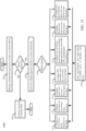
- FIG. 2 is a block diagram illustrating an example of an architecture for a PCIe interface 200.
- the root complex 204 couples a processor 202 to memory devices (e.g. the memory subsystem 208) and a PCIe switch circuit 206.
- the switch circuit 206 includes cascaded switch devices.
- One or more PCIe endpoint devices 210 may be coupled directly to the root complex 204, while other PCIe endpoint devices 212 1 , 212 2 , ...
- the root complex 212 N may be coupled to the root complex 204 through the PCIe switch circuit 206.
- the root complex 204 may be coupled to the processor 202 using a proprietary local bus interface or a standards-defined local bus interface.
- the root complex 204 may control operations of the PCIe interface 200, and may generate transaction requests for the processor 202.
- the root complex 204 is implemented in the same IC device that includes the processor 202.
- a root complex 204 may support multiple PCIe ports.
- the root complex 204 may control communication between the processor 202 the memory subsystem 208 and/or other PCIe endpoint devices 210, 212 1 , 212 2 , ... 212 N .
- An endpoint device 210, 212 1 , 212 2 , ... or 212 N may be defined as a device other than the root complex 204 that is capable of requesting or initiating a PCIe transaction, or responding to a PCIe transaction.
- the PCIe interface 200 may support full-duplex communication between any two endpoints, with no inherent limitation on concurrent access across multiple endpoints.
- Information to be communicated using the PCIe interface 200 is encapsulated in packets in accordance with PCIe bus protocols.
- Devices coupled to a PCIe bus may communicate using one or more PCIe lanes.
- a PCIe lane may be defined as a point-to-point communication channel between two PCIe ports.
- a PCIe lane may provide full-duplex communication and may include two differentially encoded pairs of signaling wires or signal traces, with one pair of wires being used for transmitting data and the other pair of wires being used for receiving data. Packets may carry information in eight-bit bytes.
- packet data may be striped across multiple lanes. The number of lanes in the multi-lane link may be negotiated during device initialization.
- FIG. 3 provides a more detailed block diagram of the components of a conventional PCIe system 300 from an integrated circuit (IC) level.
- PIPE Spec PHY Interface for PCI Express specification
- FIG. 3 provides a more detailed block diagram of the components of a conventional PCIe system 300 from an integrated circuit (IC) level.
- IC integrated circuit
- PHY Interface for PCI Express specification (“PIPE Spec") that details the use of PCIe in a PHY environment.
- PIPE Spec PHY Interface for PCI Express specification
- figures illustrating embodiments of PHY logical structures incorporate many of the logical aspects as found in the PHY Interface for PCI Express specification. Therefore, the terms MAC, PCS and PMA will be found in the PHY Interface for PCI Express specification along with conventional features and functions.
- An interface (PIPE) between the PHY and MAC layers may be found in the PHY Interface for PCI Express specification, Chapter 6.
- the PCIe system 300 includes a first IC 302, which may be an application processor (AP) system on a chip (SOC), and a second IC 304, which may be a mobile device modem (MDM) SOC.
- the first IC 302 is coupled to the second IC 304 through a PCIe bus 306.
- the PCIe bus 306 is generally a differential bus with high speed differential signaling.
- the first IC 302 may include a first MAC logic 308 and a first PHY 310 coupled by a first PIPE 312.
- the second IC 304 may include a second MAC logic 314 and a second PHY 316 coupled by a second PIPE 318.
- the first PHY 310 and the second PHY 316 are analog PHYs designed to accommodate high speed and high bandwidth.
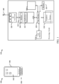
- FIG. 4 further illustrates an example of at least one MAC/PHY layer interface configuration of a PCIe device 400.
- PIPE Spec allows for various types of these interface configurations to support various signaling rates, there is a requirement that the data and logical command/status signals 402 are compliant with the "PIPE Spec," usually found in the PHY Interface for PCI Express specification, Chapter 4.
- the MAC layer 404 is generally responsible for at least the state machines for link training as well as Scrambling and Descambling.
- the PHY layer is at least generally responsible for high speed differential signaling, encoding/decoding, clock domain and analog buffers, more detail is explained below.
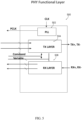
- FIG. 5 and 6 provide a more detailed illustration of exemplary PHY layer functional blocks according to the "PIPE Spec."
- the PHY layer 500 functions include PLL 502, TX layer 504 and RX layer 506.
- the functions include the Physical Media Attachment Layer (PMA) 602, also known as the Physical Sub-Block layer and generally contains the analog buffers and SERDES.
- the PMA is also generally responsible for Sideband signaling and Clock management (i.e., PLL).
- Additional functionality is generally found in the Physical Coding Sublayer (PCS) also known as a component of the Logical Sub-block.
- the PCS generally contains the capability for 8b/10b or 128b/130b encode/decode as well as RX detection and an elastic buffer.
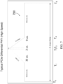
- the PCIe system 300 (see FIG. 3 ) will spend some portion of the time in a low-power mode, sometimes referred to as an idle mode or L1 state and/or L1 sub-states by the PCIe protocol.
- the first IC 302 needs to send a signal to the second IC 304
- the PCIe system 300 is moved from the L1 state (or from one of the L1 sub-states) to an L0 state, and transmission of data signals occurs.
- exemplary embodiments may accumulate data for no more than one or two microseconds.
- the PCIe system 300 is put into the L0 state and data is sent based upon the length of time the data is accumulated, which will produce many state changes in a relatively small period of time.
- the amount of data in a low-bandwidth application such as an Internet of Things (IoT) or wearable device, may be relatively low.
- IoT Internet of Things
- the amount of time to wake the PCIe system 300 and the amount of time spent putting the PCIe system 300 back into the L1 state (or one of the L1 sub-states) is comparatively large relative to the time spent transmitting.
- T0 reflects the beginning of the millisecond, and the PCIe system 300 is in one of the L1 sub-states; T1 reflects when the PCIe system 300 begins to wake; T2 represents when data transmission begins; T3 represents when data transmission ends; and T4 represents when the PCIe system 300 returns to the low-power L1 sub-state mode.
- the time T1 to T2 reflects time spent charging capacitors and letting a PLL settles.
- the time from T3 to T4 represents the time spent discharging capacitors and instructing various elements to return to the low-power L1 state (or L1 sub-state).
- the time from T1 to T4 may be as much tens of microseconds, which is a large portion of time and a significant power use. It is not uncommon for more than 60 percent and sometimes as much as 90 percent of the power expended by the PCIe system 300 to be spent during the transitions. Having as much as 90 percent of the power being spent during transitions is common amongst low-speed communications. Such a power consumption profile impacts battery life and is generally not needed for low-power applications. While a particular L1 sub-state is illustrated in FIG. 7 , it should be appreciated that comparable situations apply to other L1 sub-states and the L1 state. Accordingly, all such low-power modes may benefit from power savings according to the present disclosure.
- FIG 8 provides an illustration of exemplary timing according to the present disclosure, when the system has entered into a single-ended signaling mode from a differential signaling mode and may have removed some or all of the functions needed for differential signaling.
- This illustration shows that a data rate over-the air (i.e. 1 Mbps for LTE-M) is better matched with the PCIe data rate between the application processor 132 and the modem 130. According to the present disclosure and detailed further below, this may be achieved by not using 8b/10b encoding and removing latency from charging capacitors on the bus needed for differential signaling.
- the single-ended signaling mode also removes the latencies of going in and out of low power mode, which may save many microseconds for each transition.
- FIG. 9 illustrates a PHY layer 900 illustrating that allows for better power savings by the creation of two ancillary blocks 912, 914 in the PHY layer 910.
- the clock is always 100 MHZ, therefore one would need a PLL to synthesize a higher frequency clock and the clocking is done within the data stream which means one would need clock and data recovery on the other side.
- speed requirement is not as high as traditional PCIe needs, data can be sent synchronized with the clock being supplied in the single-ended signaling mode.
- a Low Power Physical Coding Sub-Layer (LP-PCS) 912 can be configured to shut off the decode/encode circuitry, generally the biggest consumer of power in this block. Other functions may or may not be shut off.
- LP-PMA Low Power Physical Media Attachment Sub-Layer
- LP-PMA Low Power Physical Media Attachment Sub-Layer
- Sideband signaling may be shut off. Therefore, during single ended signaling mode the LP-PMA 914 may only have a transmitter/receiver mode with buffering turned on.
- FIG. 10 illustrates another embodiment of the PHY 1010 wherein the PHY is configurable to achieve the same functionality as shown in FIG. 9 , as a combination of both the normal mode PHY layer 900 and the Low Power Mode PHY layer 910.
- the PHY 1010 may be configured such that the Configurable Physical Sublayer (C-PCS) 1012 and the Configurable Physical Media Sublayer (C-PMA) 1014 provide the differential signaling mode, distinguished as PIPE-A (via blocks 902 904) with the functionality of the PIPE-B (via blocks 912 and 914) during single ended signaling mode.
- C-PCS Configurable Physical Sublayer
- C-PMA Configurable Physical Media Sublayer
- FIG. 11A illustrates another possible embodiment for power savings during a single ended signaling mode.
- This embodiment provides configurability at the Differential connection layer 1106 and the termination pins 1108 1110.
- the Differential connection layer 1106 has configurable termination pins, which can be found as the termination pins 1108 to each of the RX, TX and CLK lines.
- a legend 1120 distinguishes what the different termination pins mean, wherein the Positive termination pins 1108 are identified. Ordinarily, a negative termination pin is not needed.
- FIG. 11B illustrates the same PHY 1100 when it is "switched" to a single-ended mode.
- the termination pins for the RX and TX lines (and/or CLK) 1110 are grounded to negative.
- the Positive pins have been removed (in terms of functionality), they will continue to exist.
- the CLK line it is also configurable, however the CLK pin will have a single-ended LVCMOS with a configurable termination pin option. This option saves power for the CLOCK line connection. For short trace length connections, differential signaling with termination could be avoided for the fixed 100MHZ clock line.
- FIG. 12A illustrates yet another possible embodiment for power savings during a single ended signaling mode.
- the Pipe-A PHY 900-Y that resembles the previously shown embodiment of Pipe-A PHY 900 of FIG. 9 , has the same PCS 902 and PMA 904.
- the distinction that is illustrated in this embodiment has to do with configurability at the sideband signals 1200.
- the previously discussed communication lines of the RX, TX and CLK, as well as the sideband signals 1200, comprise what is known in PCIe as a channel 1202 that provides point-to-point communication between two PCIe ports.
- the PCIe specific sideband signals (e.g., RESET, CLK_REQ, WAKEUP, etc.) are consolidated and handled through an in-band communication method via the singled-ended interface.
- FIG. 12B makes use of previous FIG. 10 (configurable PHY 1010) and shows that the sideband signaling 1204 is provided through the single-ended signaling mode via the CLK line.
- Sideband signals (e.g., WAKEUP) are sent only during the differential state.
- FIG. 13 illustrates an example of an architecture for a control logic 1300 capable of managing changes in the PHY for transition between Differential and single-ended signaling mode.
- the control logic 1300 can be used for either managing a system similar to the embodiments illustrated in FIG. 9 , FIG. 10 , FIG. 11A / 11B or FIG. 12A / 12B or any other combinations of these embodiments, to facilitate the configuration changes needed between differential and single-ended signaling modes. Different environments may need different power savings requirements, so it is not unreasonable to assume that the embodiments can be mixed and matched as needed. It may be done as shown by control logic 1300 or some similar managing entity within the PHY layer 900. In one embodiment, the control logic 1300 may control the PMA 904 (not shown, see FIG.
- control logic 1300 may control the PCS 902 (not shown, see FIG. 9 ) block to facilitate the capability for 8b/10b or 128b/130b encode/decode function 1304 being powered down or off when transitioning from differential to single-ended signaling modes.
- control logic 1300 may control a Physical I/O Interface block 1308 to facilitate the capability for the embodiment as shown in FIG.s 11A and 11B wherein the termination pins are either positive or negative depending upon their state of either differential or single-ended signaling modes.
- FIG. 14 illustrates the ability of the disclosure to be used at a system wide PCIe environment wherein any number of devices may be active in either a normal mode 1402 or low-power mode 1404 (through the use of the single-ended signaling embodiments).
- FIG. 15 provides a flowchart of process 1500 associated with using the PHY layer 500 of Figure 5 according to an exemplary aspect of the present disclosure.
- the process 1500 begins by exchanging messages 1502 between devices that need to communicate with each other through PCIe protocol to determine if a low power mode is capable and if so, which one. If there is not mutual agreement between the pair of devices that are planning on exchanging data or they are incompatible with one another regarding which low power state is available 1504, the devices may continue on with normal full power mode 1506. There are other conditions wherein there may not be mutual agreement, e.g., the receiving side may want to receive more data at a higher speed.
- each side will have to correspondingly configure respective PHY layer 900 to the low-power mode that was agreed by both 1510.
- Fig. 15 provides a variety of illustrations of exemplary combinations of low power modes 1512 to enable single-ended signaling as described or shown in this disclosure, this is not meant to be an exhaustive list. It is just an illustration of the varied number of low power scenarios for single-ended signaling that are available according to the disclosure.
- the PHY layer 900 will enter the single-ended signaling state to either send or receive in this mode 1520.
- the embodiments disclosed herein may be provided in or integrated into any processor-based device.
- Examples include a set top box, an entertainment unit, a navigation device, a communications device, a fixed location data unit, a mobile location data unit, a global positioning system (GPS) device, a mobile phone, a cellular phone, a smart phone, a session initiation protocol (SIP) phone, a tablet, a phablet, a server, a computer, a portable computer, a mobile computing device, a wearable computing device (e.g., a smart watch, a health or fitness tracker, eyewear, etc.), a desktop computer, a personal digital assistant (PDA), a monitor, a computer monitor, a television, a tuner, a radio, a satellite radio, a music player, a digital music player, a portable music player, a digital video player, a video player, a digital video disc (DVD) player, a portable digital video player, an automobile, a vehicle component, a
- the examples may achieve power-saving by switching between a differential a single-ended PCIe signaling.
- Clock rate may be reduced, and single-ended PCIe signaling reduces complexity in circuitry in the control block.
- the PCIe PHY may be put in an always-ready state (e.g., eliminating start-up and shut-down time and power cost).
- DSP Digital Signal Processor
- ASIC Application Specific Integrated Circuit
- FPGA Field Programmable Gate Array
- a processor may be a microprocessor, but in the alternative, the processor may be any conventional processor, controller, microcontroller, or state machine.
- a processor may also be implemented as a combination of computing devices (e.g., a combination of a DSP and a microprocessor, a plurality of microprocessors, one or more microprocessors in conjunction with a DSP core, or any other such configuration).
- RAM Random Access Memory
- ROM Read Only Memory
- EPROM Electrically Programmable ROM
- EEPROM Electrically Erasable Programmable ROM
- registers a hard disk, a removable disk, a CD-ROM, or any other form of computer readable medium known in the art.
- An exemplary storage medium is coupled to the processor such that the processor can read information from, and write information to, the storage medium.
- the storage medium may be integral to the processor.
- the processor and the storage medium may reside in an ASIC.
- the ASIC may reside in a remote station.
- the processor and the storage medium may reside as discrete components in a remote station, base station, or server.
Landscapes
- Engineering & Computer Science (AREA)
- Theoretical Computer Science (AREA)
- General Engineering & Computer Science (AREA)
- Physics & Mathematics (AREA)
- General Physics & Mathematics (AREA)
- Computer Hardware Design (AREA)
- Mathematical Physics (AREA)
- Power Sources (AREA)
- Information Transfer Systems (AREA)
Claims (9)
- Ein integrierter Schaltkreis (IC), der ausgebildet ist für eine Verbindung mit einem PCIe (Peripheral Component Interconnect (PCI) Express)-Bus, aufweisend:einen PCIe-Physikalische-Schicht-Funktionsblock (PHY) (1010), undeine PHY-Schnittstelle für PCI Express (PIPE), die aufweist:einen Steuerblock, der konfiguriert ist zum Auswählen zwischen einer differentiellen Signalisierung und einer Single-Ended-Signalisierung für den PCIe-Bus,wobei die Single-Ended-Signalisierung durch bestehende Stifte (1108, 1110) des IC, die mit dem PCIe-Bus für eine differentielle Signalisierung gekoppelt sind, gesendet werden, wenn die Single-Ended-Signalisierung für den PCIe-Bus ausgewählt ist,wobei der PHY aufweist:eine differentielle Schicht,einen Taktgenerator,eine Side-Band-Signalisierungsschicht, undeine erste konfigurierbare physikalische Codierungs-Subschicht (Configurable Physical Coding Sub-Layer bzw. C-PCS) (1012) und eine erste konfigurierbare physikalische Medienzugangsschicht (Configurable Physical Media Attachment Layer bzw. C-PMA) (1014), die die differentielle Signalisierung und die Single-Ended-Signalisierung durchführen,wobei der Steuerblock betriebsfähig ist zum Veranlassen der ersten C-PCS zu einem Wechseln zwischen der differentiellen Signalisierung und der Single-Ended-Signalisierung,dadurch gekennzeichnet, dass der Steuerblock betriebsfähig ist zum Veranlassen des PHY zum Wechseln der PCIe-Side-Band-Signalisierung zu der In-Band-Signalisierung (1204), wenn in der Single-Ended-Signalisierung, und zu der Side-Band-Signalisierung (1200), wenn in der differentiellen Signalisierung.
- IC nach Anspruch 1, wobei der Steuerblock eine Hardware-Schaltung, Software oder eine Kombination aus Hardware und Software aufweist.
- IC nach Anspruch 1, wobei der Steuerblock konfiguriert ist zum Wählen zwischen der differentiellen Signalisierung und der Single-Ended-Signalisierung basierend auf einer Durchsatzschätzung oder einem Batteriestatus.
- IC nach Anspruch 1, wobei der PHY weiterhin aufweist:eine differentielle Schicht,einen Taktgenerator, undwobei der Steuerblock konfiguriert ist zum:
Wechseln jedes des einen oder der mehreren Anschlussstifte zwischen einem positiven Anschlussmodus und einem negativen Anschlussmodus. - IC nach Anspruch 1, wobei der Steuerblock in wenigstens einem Anschlussmodus alle Kanalkommunikationsleitungen mit der Erde verbindet.
- IC nach Anspruch 1, wobei der PHY weiterhin aufweist:eine Steuerlogikschicht, undwobei der Steuerblock betrieben werden kann zum Veranlassen der Steuerlogikschicht zu einem Wechseln zwischen der differentiellen Signalisierung und der Single-Ended-Signalisierung für den PCIe-Bus.
- IC nach Anspruch 1, wobei der IC Teil eines PCIe-Systems ist, das Geräte in der differentiellen Signalisierung und der Single-Ended-Signalisierung aufweist.
- IC nach Anspruch 1, der in einem Gerät integriert ist, das aus der Gruppe ausgewählt ist, die umfasst: eine Set-Top-Box, eine Unterhaltungseinheit, ein Navigationsgerät, ein Kommunikationsgerät, eine fix positionierte Dateneinheit, eine mobile Dateneinheit, ein GPS (Global Positioning System)-Gerät, ein Mobiltelefon, ein Zellulartelefon, ein Smartphone, ein SIP (Session Initiation Protocol)-Telefon, ein Tablet, ein Phablet, einen Server, einen Computer, einen tragbaren Computer, ein mobiles Rechengerät, ein tragbares Rechengerät, einen Desktop-Computer, einen PDA (Personal Digital Assistant), einen Bildschirm, einen Computermonitor, ein Fernsehgerät, einen Tuner, ein Radiogerät, ein Satellitenradiogerät, ein Musikwiedergabegerät, ein digitales Musikwiedergabegerät, ein tragbares Musikwiedergabegerät, ein digitales Videowiedergabegerät, ein Videowiedergabegerät, ein DVD (Digital Video Disc)-Wiedergabegerät, ein tragbares digitales Videowiedergabegerät, ein Automobil, eine Fahrzeugkomponente, ein Avioniksystem, eine Drohne und einen Multicopter.
- Ein Verfahren, das durch einen integrierten Schaltkreis (IC) durchgeführt wird, der für eine Stromeinsparung optimiert ist, mit einem PCIe (Peripheral Component Interconnect (PCI) Express)-Bus gekoppelt ist und einen PCIe-Physikalische-Schicht-Funktionsblock (PHY) aufweist, der eine differentielle Schicht, einen Takterzeuger, eine Side-Band-Signalisierungsschicht und einen ersten Konfigurierbare-physikalische-Codierungs-Subschicht (Configurable Physical Coding Sub-Layer bzw. C-PCS)-Block, der eine differentielle Signalisierung und eine Single-Ended-Signalisierung durchführt, aufweist, wobei das Verfahren aufweist:Empfangen einer Anfrage für das Eintreten in einen Single-Ended-Signalisierungsmodus,Senden einer Angabe eines durch den IC zu verwendenden Modus des Single-Ended-Signalisierungsmodus,Eintreten in den Modus des Single-Ended-Signalisierungsmodus durch das Veranlassen der ersten C-PCS zum Wechseln von der differentiellen Signalisierung zu der Single-Ended-Signalisierung, undSenden über den Single-Ended-Signalisierungsmodus unter Verwendung von bestehenden Stiften des IC, die mit dem PCIe-Bus für eine differentielle Signalisierung gekoppelt sind,gekennzeichnet durch das Wechseln der PCIe-Side-Band-Signalisierung zu der In-Band-Signalisierung (1204), wenn in der Single-Ended-Signalisierung, und zu der Side-Band-Signalisierung (1200), wenn in der differentiellen Signalisierung.
Applications Claiming Priority (3)
| Application Number | Priority Date | Filing Date | Title |
|---|---|---|---|
| US201762570824P | 2017-10-11 | 2017-10-11 | |
| US16/155,824 US10963035B2 (en) | 2017-10-11 | 2018-10-09 | Low power PCIe |
| PCT/US2018/055197 WO2019075049A1 (en) | 2017-10-11 | 2018-10-10 | INTERCONNECTION OF PERIPHERAL COMPONENTS EXPRESS LOW POWER |
Publications (2)
| Publication Number | Publication Date |
|---|---|
| EP3695320A1 EP3695320A1 (de) | 2020-08-19 |
| EP3695320B1 true EP3695320B1 (de) | 2024-02-21 |
Family
ID=65993710
Family Applications (1)
| Application Number | Title | Priority Date | Filing Date |
|---|---|---|---|
| EP18795894.7A Active EP3695320B1 (de) | 2017-10-11 | 2018-10-10 | Pcie mit niedriger leistung |
Country Status (5)
| Country | Link |
|---|---|
| US (1) | US10963035B2 (de) |
| EP (1) | EP3695320B1 (de) |
| CN (1) | CN111052101B (de) |
| TW (1) | TW201923597A (de) |
| WO (1) | WO2019075049A1 (de) |
Families Citing this family (6)
| Publication number | Priority date | Publication date | Assignee | Title |
|---|---|---|---|---|
| CN111131873A (zh) * | 2019-12-26 | 2020-05-08 | 曙光网络科技有限公司 | 服务器音视频数据的处理方法及处理装置 |
| CN111615150B (zh) * | 2020-05-13 | 2023-09-08 | 深圳市广和通无线股份有限公司 | 基于PCIe接口的5G数据传输方法、装置、设备及存储介质 |
| US11789658B2 (en) | 2021-04-13 | 2023-10-17 | SK Hynix Inc. | Peripheral component interconnect express (PCIe) interface system and method of operating the same |
| KR102518317B1 (ko) | 2021-04-13 | 2023-04-06 | 에스케이하이닉스 주식회사 | PCIe 인터페이스 장치 및 그 동작 방법 |
| KR102668564B1 (ko) * | 2021-06-01 | 2024-05-24 | 에스케이하이닉스 주식회사 | PCIe 인터페이스 장치 및 그 동작 방법 |
| CN115514454B (zh) * | 2022-09-19 | 2024-05-28 | Oppo广东移动通信有限公司 | 数据传输方法及装置、电子设备、计算机可读存储介质 |
Family Cites Families (44)
| Publication number | Priority date | Publication date | Assignee | Title |
|---|---|---|---|---|
| US6243776B1 (en) * | 1998-07-13 | 2001-06-05 | International Business Machines Corporation | Selectable differential or single-ended mode bus |
| US6701280B2 (en) * | 2002-03-22 | 2004-03-02 | Guide Technology | System and method to provide measurement capabilities for both single-ended and differential signals with software switching |
| US20050259685A1 (en) * | 2004-05-21 | 2005-11-24 | Luke Chang | Dual speed interface between media access control unit and physical unit |
| US7568059B2 (en) * | 2004-07-08 | 2009-07-28 | Asocs Ltd. | Low-power reconfigurable architecture for simultaneous implementation of distinct communication standards |
| US7257655B1 (en) * | 2004-10-13 | 2007-08-14 | Altera Corporation | Embedded PCI-Express implementation |
| US7183797B2 (en) * | 2004-10-29 | 2007-02-27 | Altera Corporation | Next generation 8B10B architecture |
| US20060114918A1 (en) * | 2004-11-09 | 2006-06-01 | Junichi Ikeda | Data transfer system, data transfer method, and image apparatus system |
| JP2006338204A (ja) * | 2005-05-31 | 2006-12-14 | Toshiba Corp | 情報処理装置、および省電力制御方法 |
| JP2006343815A (ja) * | 2005-06-07 | 2006-12-21 | Matsushita Electric Ind Co Ltd | 通信装置、通信方法、通信システム |
| US20070182456A1 (en) * | 2005-11-21 | 2007-08-09 | Texas Instruments Incorporated | Reducing Pin Count When the Digital Output is to be Provided in Differential or Single-ended Form |
| US7916750B2 (en) * | 2005-12-28 | 2011-03-29 | Intel Corporation | Transaction layer packet compression |
| CN101206631B (zh) * | 2006-12-22 | 2010-09-29 | 中芯国际集成电路制造(上海)有限公司 | 高速外设部件互连接口及信号处理方法 |
| US9251873B1 (en) * | 2010-05-20 | 2016-02-02 | Kandou Labs, S.A. | Methods and systems for pin-efficient memory controller interface using vector signaling codes for chip-to-chip communications |
| US8693208B2 (en) | 2010-08-06 | 2014-04-08 | Ocz Technology Group, Inc. | PCIe bus extension system, method and interfaces therefor |
| US8395416B2 (en) * | 2010-09-21 | 2013-03-12 | Intel Corporation | Incorporating an independent logic block in a system-on-a-chip |
| JP2012146041A (ja) * | 2011-01-11 | 2012-08-02 | Hitachi Ltd | 計算機装置及び信号伝送方法 |
| KR101924836B1 (ko) * | 2011-03-23 | 2018-12-04 | 삼성전자주식회사 | 고속 인터칩 통신 장치 및 방법 |
| US9122481B2 (en) * | 2011-07-01 | 2015-09-01 | Qualcomm Incorporated | System and method for standby power reduction in a serial communication system |
| US9134909B2 (en) * | 2011-08-30 | 2015-09-15 | International Business Machines Corporation | Multiple I/O request processing in a storage system |
| US9537644B2 (en) * | 2012-02-23 | 2017-01-03 | Lattice Semiconductor Corporation | Transmitting multiple differential signals over a reduced number of physical channels |
| US9009514B2 (en) * | 2012-04-11 | 2015-04-14 | Broadcom Corporation | System and method for switching in an energy efficient network |
| US9319254B2 (en) * | 2012-08-03 | 2016-04-19 | Ati Technologies Ulc | Methods and systems for processing network messages in an accelerated processing device |
| US20140201463A1 (en) * | 2012-10-22 | 2014-07-17 | Robert G. Blankenship | High performance interconnect coherence protocol |
| KR101725536B1 (ko) * | 2013-04-17 | 2017-04-11 | 인텔 코포레이션 | Pcie 프로토콜 스택을 이용하는 저전력 phy의 동작을 위한 디바이스, 방법 및 시스템 |
| US9811487B2 (en) * | 2013-07-03 | 2017-11-07 | Cisco Technology, Inc. | Back channel support for systems with split lane swap |
| US9467120B1 (en) * | 2013-12-19 | 2016-10-11 | Altera Corporation | Power management for PCI express |
| US10073808B2 (en) * | 2013-12-26 | 2018-09-11 | Intel Corporation | Multichip package link |
| US9792243B2 (en) | 2013-12-26 | 2017-10-17 | Intel Corporation | Computer architecture to provide flexibility and/or scalability |
| US10007632B2 (en) | 2014-01-22 | 2018-06-26 | Lenovo Enterprise Solutions (Singapore) Pte. Ltd. | Computing device interface connectors for peripheral component interconnect compliant devices and other devices |
| MY173962A (en) * | 2014-03-19 | 2020-02-28 | Intel Corp | Method, apparatus and system for single-ended communication of transaction layer packets |
| MY187344A (en) * | 2014-03-20 | 2021-09-22 | Intel Corp | Method, apparatus and system for configuring a protocol stack of an integrated circuit chip |
| US9766692B2 (en) * | 2014-08-01 | 2017-09-19 | Apple Inc. | Physical layer for peripheral interconnect with reduced power and area |
| US9720866B2 (en) * | 2014-09-11 | 2017-08-01 | Kabushiki Kaisha Toshiba | Interface circuit executing protocol control in compliance with first and second interface standards |
| US9747245B2 (en) * | 2014-12-17 | 2017-08-29 | Intel Corporation | Method, apparatus and system for integrating devices in a root complex |
| US20160216758A1 (en) * | 2015-01-27 | 2016-07-28 | Avago Technologies General Ip (Singapore) Pte. Ltd. | PCI Express Device With Early Low Power State |
| US9747236B2 (en) * | 2015-04-07 | 2017-08-29 | Vanco International, Llc | HDMI extender with bidirectional power over twisted pair |
| US9858237B2 (en) | 2015-05-11 | 2018-01-02 | Dell Products L.P. | Information handling system differential signalling variable bandwidth interface selectively configuring single ended and differential signals |
| US10162779B2 (en) * | 2015-05-11 | 2018-12-25 | Dell Products L.P. | Increasing data throughput of a universal serial bus (USB) type-C port |
| US9900164B2 (en) * | 2015-06-10 | 2018-02-20 | Cisco Technology, Inc. | Dynamic power management |
| US10678736B2 (en) * | 2015-09-25 | 2020-06-09 | Intel Corporation | Extending multichip package link off package |
| US10198394B2 (en) * | 2016-05-24 | 2019-02-05 | Intel Corporation | Reduced pin count interface |
| US10713202B2 (en) * | 2016-05-25 | 2020-07-14 | Samsung Electronics Co., Ltd. | Quality of service (QOS)-aware input/output (IO) management for peripheral component interconnect express (PCIE) storage system with reconfigurable multi-ports |
| CN109844725B (zh) * | 2016-07-01 | 2023-07-25 | 英特尔公司 | 点对点互连中的非对称通道 |
| US11132323B2 (en) * | 2017-06-20 | 2021-09-28 | Intel Corporation | System, apparatus and method for extended communication modes for a multi-drop interconnect |
-
2018
- 2018-10-09 US US16/155,824 patent/US10963035B2/en active Active
- 2018-10-10 CN CN201880057566.4A patent/CN111052101B/zh active Active
- 2018-10-10 EP EP18795894.7A patent/EP3695320B1/de active Active
- 2018-10-10 WO PCT/US2018/055197 patent/WO2019075049A1/en not_active Ceased
- 2018-10-11 TW TW107135737A patent/TW201923597A/zh unknown
Also Published As
| Publication number | Publication date |
|---|---|
| EP3695320A1 (de) | 2020-08-19 |
| WO2019075049A1 (en) | 2019-04-18 |
| CN111052101B (zh) | 2023-11-14 |
| TW201923597A (zh) | 2019-06-16 |
| CN111052101A (zh) | 2020-04-21 |
| US10963035B2 (en) | 2021-03-30 |
| US20190107882A1 (en) | 2019-04-11 |
Similar Documents
| Publication | Publication Date | Title |
|---|---|---|
| EP3695320B1 (de) | Pcie mit niedriger leistung | |
| CN108713197A (zh) | 用于最优性能和功率节省的自适应快速外围组件互连链路子状态发起 | |
| US8972640B2 (en) | Controlling a physical link of a first protocol using an extended capability structure of a second protocol | |
| US9830292B2 (en) | Architected protocol for changing link operating mode | |
| US8527805B2 (en) | Inter-processor communication channel including power-down functionality | |
| US20200008144A1 (en) | Link speed control systems for power optimization | |
| US20050097378A1 (en) | Method and system for power management in a gigabit Ethernet chip | |
| TW201606511A (zh) | 用於晶片至晶片通信之系統及方法 | |
| US20170364141A1 (en) | Physical Layer for Peripheral Interconnect with Reduced Power and Area | |
| CN104380274A (zh) | 优化的链路训练及管理机制 | |
| US20180357067A1 (en) | In-band hardware reset for virtual general purpose input/output interface | |
| US8661171B1 (en) | Host-slave interface for wireless communication circuit | |
| US20250021153A1 (en) | Adaptive low-power signaling to enable link signal error recovery without increased link clock rates | |
| CN120641885A (zh) | 用于聚合器-分散器的用于进入和退出低功耗模式的系统及方法 |
Legal Events
| Date | Code | Title | Description |
|---|---|---|---|
| STAA | Information on the status of an ep patent application or granted ep patent |
Free format text: STATUS: UNKNOWN |
|
| STAA | Information on the status of an ep patent application or granted ep patent |
Free format text: STATUS: THE INTERNATIONAL PUBLICATION HAS BEEN MADE |
|
| PUAI | Public reference made under article 153(3) epc to a published international application that has entered the european phase |
Free format text: ORIGINAL CODE: 0009012 |
|
| STAA | Information on the status of an ep patent application or granted ep patent |
Free format text: STATUS: REQUEST FOR EXAMINATION WAS MADE |
|
| 17P | Request for examination filed |
Effective date: 20200305 |
|
| AK | Designated contracting states |
Kind code of ref document: A1 Designated state(s): AL AT BE BG CH CY CZ DE DK EE ES FI FR GB GR HR HU IE IS IT LI LT LU LV MC MK MT NL NO PL PT RO RS SE SI SK SM TR |
|
| AX | Request for extension of the european patent |
Extension state: BA ME |
|
| DAV | Request for validation of the european patent (deleted) | ||
| DAX | Request for extension of the european patent (deleted) | ||
| STAA | Information on the status of an ep patent application or granted ep patent |
Free format text: STATUS: EXAMINATION IS IN PROGRESS |
|
| 17Q | First examination report despatched |
Effective date: 20210311 |
|
| GRAP | Despatch of communication of intention to grant a patent |
Free format text: ORIGINAL CODE: EPIDOSNIGR1 |
|
| STAA | Information on the status of an ep patent application or granted ep patent |
Free format text: STATUS: GRANT OF PATENT IS INTENDED |
|
| INTG | Intention to grant announced |
Effective date: 20231009 |
|
| GRAS | Grant fee paid |
Free format text: ORIGINAL CODE: EPIDOSNIGR3 |
|
| GRAA | (expected) grant |
Free format text: ORIGINAL CODE: 0009210 |
|
| STAA | Information on the status of an ep patent application or granted ep patent |
Free format text: STATUS: THE PATENT HAS BEEN GRANTED |
|
| AK | Designated contracting states |
Kind code of ref document: B1 Designated state(s): AL AT BE BG CH CY CZ DE DK EE ES FI FR GB GR HR HU IE IS IT LI LT LU LV MC MK MT NL NO PL PT RO RS SE SI SK SM TR |
|
| REG | Reference to a national code |
Ref country code: GB Ref legal event code: FG4D |
|
| REG | Reference to a national code |
Ref country code: CH Ref legal event code: EP |
|
| REG | Reference to a national code |
Ref country code: IE Ref legal event code: FG4D |
|
| REG | Reference to a national code |
Ref country code: DE Ref legal event code: R096 Ref document number: 602018065580 Country of ref document: DE |
|
| REG | Reference to a national code |
Ref country code: LT Ref legal event code: MG9D |
|
| REG | Reference to a national code |
Ref country code: NL Ref legal event code: MP Effective date: 20240221 |
|
| PG25 | Lapsed in a contracting state [announced via postgrant information from national office to epo] |
Ref country code: IS Free format text: LAPSE BECAUSE OF FAILURE TO SUBMIT A TRANSLATION OF THE DESCRIPTION OR TO PAY THE FEE WITHIN THE PRESCRIBED TIME-LIMIT Effective date: 20240621 |
|
| PG25 | Lapsed in a contracting state [announced via postgrant information from national office to epo] |
Ref country code: LT Free format text: LAPSE BECAUSE OF FAILURE TO SUBMIT A TRANSLATION OF THE DESCRIPTION OR TO PAY THE FEE WITHIN THE PRESCRIBED TIME-LIMIT Effective date: 20240221 |
|
| PG25 | Lapsed in a contracting state [announced via postgrant information from national office to epo] |
Ref country code: GR Free format text: LAPSE BECAUSE OF FAILURE TO SUBMIT A TRANSLATION OF THE DESCRIPTION OR TO PAY THE FEE WITHIN THE PRESCRIBED TIME-LIMIT Effective date: 20240522 |
|
| REG | Reference to a national code |
Ref country code: AT Ref legal event code: MK05 Ref document number: 1659712 Country of ref document: AT Kind code of ref document: T Effective date: 20240221 |
|
| PG25 | Lapsed in a contracting state [announced via postgrant information from national office to epo] |
Ref country code: HR Free format text: LAPSE BECAUSE OF FAILURE TO SUBMIT A TRANSLATION OF THE DESCRIPTION OR TO PAY THE FEE WITHIN THE PRESCRIBED TIME-LIMIT Effective date: 20240221 Ref country code: RS Free format text: LAPSE BECAUSE OF FAILURE TO SUBMIT A TRANSLATION OF THE DESCRIPTION OR TO PAY THE FEE WITHIN THE PRESCRIBED TIME-LIMIT Effective date: 20240521 Ref country code: NL Free format text: LAPSE BECAUSE OF FAILURE TO SUBMIT A TRANSLATION OF THE DESCRIPTION OR TO PAY THE FEE WITHIN THE PRESCRIBED TIME-LIMIT Effective date: 20240221 |
|
| PG25 | Lapsed in a contracting state [announced via postgrant information from national office to epo] |
Ref country code: ES Free format text: LAPSE BECAUSE OF FAILURE TO SUBMIT A TRANSLATION OF THE DESCRIPTION OR TO PAY THE FEE WITHIN THE PRESCRIBED TIME-LIMIT Effective date: 20240221 |
|
| PG25 | Lapsed in a contracting state [announced via postgrant information from national office to epo] |
Ref country code: AT Free format text: LAPSE BECAUSE OF FAILURE TO SUBMIT A TRANSLATION OF THE DESCRIPTION OR TO PAY THE FEE WITHIN THE PRESCRIBED TIME-LIMIT Effective date: 20240221 |
|
| PG25 | Lapsed in a contracting state [announced via postgrant information from national office to epo] |
Ref country code: RS Free format text: LAPSE BECAUSE OF FAILURE TO SUBMIT A TRANSLATION OF THE DESCRIPTION OR TO PAY THE FEE WITHIN THE PRESCRIBED TIME-LIMIT Effective date: 20240521 Ref country code: NO Free format text: LAPSE BECAUSE OF FAILURE TO SUBMIT A TRANSLATION OF THE DESCRIPTION OR TO PAY THE FEE WITHIN THE PRESCRIBED TIME-LIMIT Effective date: 20240521 Ref country code: NL Free format text: LAPSE BECAUSE OF FAILURE TO SUBMIT A TRANSLATION OF THE DESCRIPTION OR TO PAY THE FEE WITHIN THE PRESCRIBED TIME-LIMIT Effective date: 20240221 Ref country code: LT Free format text: LAPSE BECAUSE OF FAILURE TO SUBMIT A TRANSLATION OF THE DESCRIPTION OR TO PAY THE FEE WITHIN THE PRESCRIBED TIME-LIMIT Effective date: 20240221 Ref country code: IS Free format text: LAPSE BECAUSE OF FAILURE TO SUBMIT A TRANSLATION OF THE DESCRIPTION OR TO PAY THE FEE WITHIN THE PRESCRIBED TIME-LIMIT Effective date: 20240621 Ref country code: HR Free format text: LAPSE BECAUSE OF FAILURE TO SUBMIT A TRANSLATION OF THE DESCRIPTION OR TO PAY THE FEE WITHIN THE PRESCRIBED TIME-LIMIT Effective date: 20240221 Ref country code: GR Free format text: LAPSE BECAUSE OF FAILURE TO SUBMIT A TRANSLATION OF THE DESCRIPTION OR TO PAY THE FEE WITHIN THE PRESCRIBED TIME-LIMIT Effective date: 20240522 Ref country code: FI Free format text: LAPSE BECAUSE OF FAILURE TO SUBMIT A TRANSLATION OF THE DESCRIPTION OR TO PAY THE FEE WITHIN THE PRESCRIBED TIME-LIMIT Effective date: 20240221 Ref country code: ES Free format text: LAPSE BECAUSE OF FAILURE TO SUBMIT A TRANSLATION OF THE DESCRIPTION OR TO PAY THE FEE WITHIN THE PRESCRIBED TIME-LIMIT Effective date: 20240221 Ref country code: BG Free format text: LAPSE BECAUSE OF FAILURE TO SUBMIT A TRANSLATION OF THE DESCRIPTION OR TO PAY THE FEE WITHIN THE PRESCRIBED TIME-LIMIT Effective date: 20240221 Ref country code: AT Free format text: LAPSE BECAUSE OF FAILURE TO SUBMIT A TRANSLATION OF THE DESCRIPTION OR TO PAY THE FEE WITHIN THE PRESCRIBED TIME-LIMIT Effective date: 20240221 |
|
| PG25 | Lapsed in a contracting state [announced via postgrant information from national office to epo] |
Ref country code: PL Free format text: LAPSE BECAUSE OF FAILURE TO SUBMIT A TRANSLATION OF THE DESCRIPTION OR TO PAY THE FEE WITHIN THE PRESCRIBED TIME-LIMIT Effective date: 20240221 Ref country code: PT Free format text: LAPSE BECAUSE OF FAILURE TO SUBMIT A TRANSLATION OF THE DESCRIPTION OR TO PAY THE FEE WITHIN THE PRESCRIBED TIME-LIMIT Effective date: 20240621 |
|
| PG25 | Lapsed in a contracting state [announced via postgrant information from national office to epo] |
Ref country code: SE Free format text: LAPSE BECAUSE OF FAILURE TO SUBMIT A TRANSLATION OF THE DESCRIPTION OR TO PAY THE FEE WITHIN THE PRESCRIBED TIME-LIMIT Effective date: 20240221 Ref country code: PT Free format text: LAPSE BECAUSE OF FAILURE TO SUBMIT A TRANSLATION OF THE DESCRIPTION OR TO PAY THE FEE WITHIN THE PRESCRIBED TIME-LIMIT Effective date: 20240621 Ref country code: PL Free format text: LAPSE BECAUSE OF FAILURE TO SUBMIT A TRANSLATION OF THE DESCRIPTION OR TO PAY THE FEE WITHIN THE PRESCRIBED TIME-LIMIT Effective date: 20240221 Ref country code: LV Free format text: LAPSE BECAUSE OF FAILURE TO SUBMIT A TRANSLATION OF THE DESCRIPTION OR TO PAY THE FEE WITHIN THE PRESCRIBED TIME-LIMIT Effective date: 20240221 |
|
| PG25 | Lapsed in a contracting state [announced via postgrant information from national office to epo] |
Ref country code: DK Free format text: LAPSE BECAUSE OF FAILURE TO SUBMIT A TRANSLATION OF THE DESCRIPTION OR TO PAY THE FEE WITHIN THE PRESCRIBED TIME-LIMIT Effective date: 20240221 |
|
| PG25 | Lapsed in a contracting state [announced via postgrant information from national office to epo] |
Ref country code: SM Free format text: LAPSE BECAUSE OF FAILURE TO SUBMIT A TRANSLATION OF THE DESCRIPTION OR TO PAY THE FEE WITHIN THE PRESCRIBED TIME-LIMIT Effective date: 20240221 |
|
| PG25 | Lapsed in a contracting state [announced via postgrant information from national office to epo] |
Ref country code: CZ Free format text: LAPSE BECAUSE OF FAILURE TO SUBMIT A TRANSLATION OF THE DESCRIPTION OR TO PAY THE FEE WITHIN THE PRESCRIBED TIME-LIMIT Effective date: 20240221 Ref country code: EE Free format text: LAPSE BECAUSE OF FAILURE TO SUBMIT A TRANSLATION OF THE DESCRIPTION OR TO PAY THE FEE WITHIN THE PRESCRIBED TIME-LIMIT Effective date: 20240221 |
|
| PG25 | Lapsed in a contracting state [announced via postgrant information from national office to epo] |
Ref country code: SK Free format text: LAPSE BECAUSE OF FAILURE TO SUBMIT A TRANSLATION OF THE DESCRIPTION OR TO PAY THE FEE WITHIN THE PRESCRIBED TIME-LIMIT Effective date: 20240221 |
|
| PG25 | Lapsed in a contracting state [announced via postgrant information from national office to epo] |
Ref country code: SM Free format text: LAPSE BECAUSE OF FAILURE TO SUBMIT A TRANSLATION OF THE DESCRIPTION OR TO PAY THE FEE WITHIN THE PRESCRIBED TIME-LIMIT Effective date: 20240221 Ref country code: SK Free format text: LAPSE BECAUSE OF FAILURE TO SUBMIT A TRANSLATION OF THE DESCRIPTION OR TO PAY THE FEE WITHIN THE PRESCRIBED TIME-LIMIT Effective date: 20240221 Ref country code: RO Free format text: LAPSE BECAUSE OF FAILURE TO SUBMIT A TRANSLATION OF THE DESCRIPTION OR TO PAY THE FEE WITHIN THE PRESCRIBED TIME-LIMIT Effective date: 20240221 Ref country code: EE Free format text: LAPSE BECAUSE OF FAILURE TO SUBMIT A TRANSLATION OF THE DESCRIPTION OR TO PAY THE FEE WITHIN THE PRESCRIBED TIME-LIMIT Effective date: 20240221 Ref country code: DK Free format text: LAPSE BECAUSE OF FAILURE TO SUBMIT A TRANSLATION OF THE DESCRIPTION OR TO PAY THE FEE WITHIN THE PRESCRIBED TIME-LIMIT Effective date: 20240221 Ref country code: CZ Free format text: LAPSE BECAUSE OF FAILURE TO SUBMIT A TRANSLATION OF THE DESCRIPTION OR TO PAY THE FEE WITHIN THE PRESCRIBED TIME-LIMIT Effective date: 20240221 |
|
| REG | Reference to a national code |
Ref country code: DE Ref legal event code: R097 Ref document number: 602018065580 Country of ref document: DE |
|
| PG25 | Lapsed in a contracting state [announced via postgrant information from national office to epo] |
Ref country code: IT Free format text: LAPSE BECAUSE OF FAILURE TO SUBMIT A TRANSLATION OF THE DESCRIPTION OR TO PAY THE FEE WITHIN THE PRESCRIBED TIME-LIMIT Effective date: 20240221 |
|
| PLBE | No opposition filed within time limit |
Free format text: ORIGINAL CODE: 0009261 |
|
| STAA | Information on the status of an ep patent application or granted ep patent |
Free format text: STATUS: NO OPPOSITION FILED WITHIN TIME LIMIT |
|
| PG25 | Lapsed in a contracting state [announced via postgrant information from national office to epo] |
Ref country code: IT Free format text: LAPSE BECAUSE OF FAILURE TO SUBMIT A TRANSLATION OF THE DESCRIPTION OR TO PAY THE FEE WITHIN THE PRESCRIBED TIME-LIMIT Effective date: 20240221 |
|
| 26N | No opposition filed |
Effective date: 20241122 |
|
| PG25 | Lapsed in a contracting state [announced via postgrant information from national office to epo] |
Ref country code: SI Free format text: LAPSE BECAUSE OF FAILURE TO SUBMIT A TRANSLATION OF THE DESCRIPTION OR TO PAY THE FEE WITHIN THE PRESCRIBED TIME-LIMIT Effective date: 20240221 |
|
| REG | Reference to a national code |
Ref country code: CH Ref legal event code: PL |
|
| PG25 | Lapsed in a contracting state [announced via postgrant information from national office to epo] |
Ref country code: MC Free format text: LAPSE BECAUSE OF FAILURE TO SUBMIT A TRANSLATION OF THE DESCRIPTION OR TO PAY THE FEE WITHIN THE PRESCRIBED TIME-LIMIT Effective date: 20240221 |
|
| PG25 | Lapsed in a contracting state [announced via postgrant information from national office to epo] |
Ref country code: BE Free format text: LAPSE BECAUSE OF NON-PAYMENT OF DUE FEES Effective date: 20241031 Ref country code: LU Free format text: LAPSE BECAUSE OF NON-PAYMENT OF DUE FEES Effective date: 20241010 |
|
| PG25 | Lapsed in a contracting state [announced via postgrant information from national office to epo] |
Ref country code: CH Free format text: LAPSE BECAUSE OF NON-PAYMENT OF DUE FEES Effective date: 20241031 |
|
| REG | Reference to a national code |
Ref country code: BE Ref legal event code: MM Effective date: 20241031 |
|
| PGFP | Annual fee paid to national office [announced via postgrant information from national office to epo] |
Ref country code: GB Payment date: 20250911 Year of fee payment: 8 |
|
| PGFP | Annual fee paid to national office [announced via postgrant information from national office to epo] |
Ref country code: FR Payment date: 20250912 Year of fee payment: 8 |
|
| PG25 | Lapsed in a contracting state [announced via postgrant information from national office to epo] |
Ref country code: IE Free format text: LAPSE BECAUSE OF NON-PAYMENT OF DUE FEES Effective date: 20241010 |
|
| PGFP | Annual fee paid to national office [announced via postgrant information from national office to epo] |
Ref country code: DE Payment date: 20250912 Year of fee payment: 8 |
|
| PG25 | Lapsed in a contracting state [announced via postgrant information from national office to epo] |
Ref country code: CY Free format text: LAPSE BECAUSE OF FAILURE TO SUBMIT A TRANSLATION OF THE DESCRIPTION OR TO PAY THE FEE WITHIN THE PRESCRIBED TIME-LIMIT; INVALID AB INITIO Effective date: 20181010 |