EP3694093A1 - Power conversion circuit - Google Patents
Power conversion circuit Download PDFInfo
- Publication number
- EP3694093A1 EP3694093A1 EP18864523.8A EP18864523A EP3694093A1 EP 3694093 A1 EP3694093 A1 EP 3694093A1 EP 18864523 A EP18864523 A EP 18864523A EP 3694093 A1 EP3694093 A1 EP 3694093A1
- Authority
- EP
- European Patent Office
- Prior art keywords
- semiconductor switching
- power conversion
- control
- switching elements
- switching element
- Prior art date
- Legal status (The legal status is an assumption and is not a legal conclusion. Google has not performed a legal analysis and makes no representation as to the accuracy of the status listed.)
- Granted
Links
Images





Classifications
-
- H—ELECTRICITY
- H02—GENERATION; CONVERSION OR DISTRIBUTION OF ELECTRIC POWER
- H02M—APPARATUS FOR CONVERSION BETWEEN AC AND AC, BETWEEN AC AND DC, OR BETWEEN DC AND DC, AND FOR USE WITH MAINS OR SIMILAR POWER SUPPLY SYSTEMS; CONVERSION OF DC OR AC INPUT POWER INTO SURGE OUTPUT POWER; CONTROL OR REGULATION THEREOF
- H02M1/00—Details of apparatus for conversion
- H02M1/08—Circuits specially adapted for the generation of control voltages for semiconductor devices incorporated in static converters
-
- H—ELECTRICITY
- H02—GENERATION; CONVERSION OR DISTRIBUTION OF ELECTRIC POWER
- H02M—APPARATUS FOR CONVERSION BETWEEN AC AND AC, BETWEEN AC AND DC, OR BETWEEN DC AND DC, AND FOR USE WITH MAINS OR SIMILAR POWER SUPPLY SYSTEMS; CONVERSION OF DC OR AC INPUT POWER INTO SURGE OUTPUT POWER; CONTROL OR REGULATION THEREOF
- H02M1/00—Details of apparatus for conversion
- H02M1/0003—Details of control, feedback or regulation circuits
- H02M1/0006—Arrangements for supplying an adequate voltage to the control circuit of converters
-
- H—ELECTRICITY
- H02—GENERATION; CONVERSION OR DISTRIBUTION OF ELECTRIC POWER
- H02M—APPARATUS FOR CONVERSION BETWEEN AC AND AC, BETWEEN AC AND DC, OR BETWEEN DC AND DC, AND FOR USE WITH MAINS OR SIMILAR POWER SUPPLY SYSTEMS; CONVERSION OF DC OR AC INPUT POWER INTO SURGE OUTPUT POWER; CONTROL OR REGULATION THEREOF
- H02M1/00—Details of apparatus for conversion
- H02M1/0048—Circuits or arrangements for reducing losses
-
- H—ELECTRICITY
- H02—GENERATION; CONVERSION OR DISTRIBUTION OF ELECTRIC POWER
- H02M—APPARATUS FOR CONVERSION BETWEEN AC AND AC, BETWEEN AC AND DC, OR BETWEEN DC AND DC, AND FOR USE WITH MAINS OR SIMILAR POWER SUPPLY SYSTEMS; CONVERSION OF DC OR AC INPUT POWER INTO SURGE OUTPUT POWER; CONTROL OR REGULATION THEREOF
- H02M1/00—Details of apparatus for conversion
- H02M1/08—Circuits specially adapted for the generation of control voltages for semiconductor devices incorporated in static converters
- H02M1/088—Circuits specially adapted for the generation of control voltages for semiconductor devices incorporated in static converters for the simultaneous control of series or parallel connected semiconductor devices
- H02M1/096—Circuits specially adapted for the generation of control voltages for semiconductor devices incorporated in static converters for the simultaneous control of series or parallel connected semiconductor devices the power supply of the control circuit being connected in parallel to the main switching element
-
- H—ELECTRICITY
- H02—GENERATION; CONVERSION OR DISTRIBUTION OF ELECTRIC POWER
- H02M—APPARATUS FOR CONVERSION BETWEEN AC AND AC, BETWEEN AC AND DC, OR BETWEEN DC AND DC, AND FOR USE WITH MAINS OR SIMILAR POWER SUPPLY SYSTEMS; CONVERSION OF DC OR AC INPUT POWER INTO SURGE OUTPUT POWER; CONTROL OR REGULATION THEREOF
- H02M3/00—Conversion of DC power input into DC power output
- H02M3/22—Conversion of DC power input into DC power output with intermediate conversion into AC
- H02M3/24—Conversion of DC power input into DC power output with intermediate conversion into AC by static converters
- H02M3/28—Conversion of DC power input into DC power output with intermediate conversion into AC by static converters using discharge tubes with control electrode or semiconductor devices with control electrode to produce the intermediate AC
- H02M3/325—Conversion of DC power input into DC power output with intermediate conversion into AC by static converters using discharge tubes with control electrode or semiconductor devices with control electrode to produce the intermediate AC using devices of a triode or a transistor type requiring continuous application of a control signal
- H02M3/335—Conversion of DC power input into DC power output with intermediate conversion into AC by static converters using discharge tubes with control electrode or semiconductor devices with control electrode to produce the intermediate AC using devices of a triode or a transistor type requiring continuous application of a control signal using semiconductor devices only
- H02M3/33569—Conversion of DC power input into DC power output with intermediate conversion into AC by static converters using discharge tubes with control electrode or semiconductor devices with control electrode to produce the intermediate AC using devices of a triode or a transistor type requiring continuous application of a control signal using semiconductor devices only having several active switching elements
- H02M3/33571—Half-bridge at primary side of an isolation transformer
-
- H—ELECTRICITY
- H02—GENERATION; CONVERSION OR DISTRIBUTION OF ELECTRIC POWER
- H02M—APPARATUS FOR CONVERSION BETWEEN AC AND AC, BETWEEN AC AND DC, OR BETWEEN DC AND DC, AND FOR USE WITH MAINS OR SIMILAR POWER SUPPLY SYSTEMS; CONVERSION OF DC OR AC INPUT POWER INTO SURGE OUTPUT POWER; CONTROL OR REGULATION THEREOF
- H02M3/00—Conversion of DC power input into DC power output
- H02M3/22—Conversion of DC power input into DC power output with intermediate conversion into AC
- H02M3/24—Conversion of DC power input into DC power output with intermediate conversion into AC by static converters
- H02M3/28—Conversion of DC power input into DC power output with intermediate conversion into AC by static converters using discharge tubes with control electrode or semiconductor devices with control electrode to produce the intermediate AC
- H02M3/325—Conversion of DC power input into DC power output with intermediate conversion into AC by static converters using discharge tubes with control electrode or semiconductor devices with control electrode to produce the intermediate AC using devices of a triode or a transistor type requiring continuous application of a control signal
- H02M3/335—Conversion of DC power input into DC power output with intermediate conversion into AC by static converters using discharge tubes with control electrode or semiconductor devices with control electrode to produce the intermediate AC using devices of a triode or a transistor type requiring continuous application of a control signal using semiconductor devices only
- H02M3/33569—Conversion of DC power input into DC power output with intermediate conversion into AC by static converters using discharge tubes with control electrode or semiconductor devices with control electrode to produce the intermediate AC using devices of a triode or a transistor type requiring continuous application of a control signal using semiconductor devices only having several active switching elements
- H02M3/33573—Full-bridge at primary side of an isolation transformer
-
- H—ELECTRICITY
- H02—GENERATION; CONVERSION OR DISTRIBUTION OF ELECTRIC POWER
- H02M—APPARATUS FOR CONVERSION BETWEEN AC AND AC, BETWEEN AC AND DC, OR BETWEEN DC AND DC, AND FOR USE WITH MAINS OR SIMILAR POWER SUPPLY SYSTEMS; CONVERSION OF DC OR AC INPUT POWER INTO SURGE OUTPUT POWER; CONTROL OR REGULATION THEREOF
- H02M7/00—Conversion of AC power input into DC power output; Conversion of DC power input into AC power output
- H02M7/003—Constructional details, e.g. physical layout, assembly, wiring or busbar connections
-
- H—ELECTRICITY
- H05—ELECTRIC TECHNIQUES NOT OTHERWISE PROVIDED FOR
- H05K—PRINTED CIRCUITS; CASINGS OR CONSTRUCTIONAL DETAILS OF ELECTRIC APPARATUS; MANUFACTURE OF ASSEMBLAGES OF ELECTRICAL COMPONENTS
- H05K1/00—Printed circuits
- H05K1/02—Details
- H05K1/0213—Electrical arrangements not otherwise provided for
- H05K1/0263—High current adaptations, e.g. printed high current conductors or using auxiliary non-printed means; Fine and coarse circuit patterns on one circuit board
- H05K1/0265—High current adaptations, e.g. printed high current conductors or using auxiliary non-printed means; Fine and coarse circuit patterns on one circuit board characterized by the lay-out of or details of the printed conductors, e.g. reinforced conductors, redundant conductors, conductors having different cross-sections
-
- H—ELECTRICITY
- H05—ELECTRIC TECHNIQUES NOT OTHERWISE PROVIDED FOR
- H05K—PRINTED CIRCUITS; CASINGS OR CONSTRUCTIONAL DETAILS OF ELECTRIC APPARATUS; MANUFACTURE OF ASSEMBLAGES OF ELECTRICAL COMPONENTS
- H05K2201/00—Indexing scheme relating to printed circuits covered by H05K1/00
- H05K2201/10—Details of components or other objects attached to or integrated in a printed circuit board
- H05K2201/10007—Types of components
- H05K2201/10166—Transistor
-
- Y—GENERAL TAGGING OF NEW TECHNOLOGICAL DEVELOPMENTS; GENERAL TAGGING OF CROSS-SECTIONAL TECHNOLOGIES SPANNING OVER SEVERAL SECTIONS OF THE IPC; TECHNICAL SUBJECTS COVERED BY FORMER USPC CROSS-REFERENCE ART COLLECTIONS [XRACs] AND DIGESTS
- Y02—TECHNOLOGIES OR APPLICATIONS FOR MITIGATION OR ADAPTATION AGAINST CLIMATE CHANGE
- Y02B—CLIMATE CHANGE MITIGATION TECHNOLOGIES RELATED TO BUILDINGS, e.g. HOUSING, HOUSE APPLIANCES OR RELATED END-USER APPLICATIONS
- Y02B70/00—Technologies for an efficient end-user side electric power management and consumption
- Y02B70/10—Technologies improving the efficiency by using switched-mode power supplies [SMPS], i.e. efficient power electronics conversion e.g. power factor correction or reduction of losses in power supplies or efficient standby modes
Definitions
- the present invention relates to a power conversion circuit for a power conversion device including a plurality of semiconductor switching elements, and more particularly, to a configuration of each of circuit board patterns for isolated circuits configured to drive the semiconductor switching elements.
- Power conversion devices often adopt a circuit of a half-bridge configuration, in which semiconductor switching elements are connected to each other in series.
- Drive circuits for the series-connected semiconductor switching elements are required to have different GNDs (reference potentials), and are achieved by, for example, isolated power supply circuits.
- GNDs reference potentials
- the respective circuits are required to be isolated from a housing, and a GND different from that of the housing is required as a GND for a semiconductor switching element of a lower arm in the half-bridge configuration.
- a common GND can be used for semiconductor switching elements of lower arms of the two half-bridge configurations.
- different GNDs are required for semiconductor switching elements of upper arms thereof, with the result that the requisite number of GNDs for different nodes increases (see, for example, Patent Literature 1 and Patent Literature 2).
- an inverter circuit has three half-bridge configurations including three upper-arm semiconductor switching elements, and three lower-arm semiconductor switching elements. Further, in Patent Literature 1, GNDs and power supplies for four different nodes in total are provided in the form of being isolated by optical means.
- Patent Literature 2 three half-bridge configurations are provided. Further, in Patent Literature 2, a bootstrapping configuration is employed for one of the half-bridge configurations of three inverter circuits, and hence a common power supply is used for driving circuits for semiconductor switching elements of upper and lower arms thereof. In other words, in the configuration of Patent Literature 2, it is required to provide GNDs for every different node, and the inverter circuits are required to have GNDs for four different nodes in total.
- a GND is formed with use of a solid pattern.
- the solid pattern is obtained by filling a large area.
- those GNDs for different nodes overlap one another in plan view, that is, as viewed from a direction orthogonal to a circuit board surface in many cases.
- a consideration is made of a case of using a semiconductor switching element made of gallium nitride (GaN) or silicon carbide (SiC) having a wide bandgap.
- the wide-bandgap semiconductor has a feature of being capable of high-speed operation, and thus enables high-frequency switching. With this configuration, a power conversion device can be made compact by downsizing respective peripheral passive components.
- parasitic capacitors are formed therebetween.
- a GND used for driving a semiconductor switching element of a lower arm and a GND used for driving a semiconductor switching element of an upper arm in the half-bridge circuit overlap each other in plan view
- a voltage between the GNDs overlapping in plan view varies depending on a switching period, and hence a parasitic capacitor therebetween is charged/discharged.
- charges are accumulated/released via any semiconductor switching element in an ON state, resulting in a problem of increasing a loss of the semiconductor switching element.
- the semiconductor switching element having a wide bandgap achieves a high switching speed. This leads to a higher charging/discharging speed in parasitic capacitors between the plurality of GNDs for different nodes. Due to an influence of an electric current flowing during charging/discharging of each parasitic capacitor, a voltage drop occurs in a parasitic inductance portion of a GND wiring between a driver and a corresponding semiconductor switching element. This causes a problem that noise is superimposed on a gate of the semiconductor switching element, and the operation thereof becomes unstable.
- the present invention has been made to solve the problems described above, and an object of the present invention is generally to obtain a power conversion circuit for achieving a power conversion device capable of suppressing charging/discharging of a parasitic capacitor caused by high-frequency switching, and of reducing a loss of a semiconductor switching element that is not limited to a wide-bandgap semiconductor switching element.
- a power conversion circuit including: a circuit board including a plurality of layers including two or more layers, on which circuit patterns are formed; and a plurality of semiconductor switching elements connected to the circuit patterns of the circuit board, and configured to perform switching for power conversion.
- a plurality of control ground patterns for different nodes which are configured to drive the plurality of semiconductor switching elements, are arranged so as not to overlap one another in plan view.
- the circuit patterns for the plurality of GNDs for different nodes used to drive the semiconductor switching elements are arranged so as not to overlap one another in plan view. With this configuration, it is possible to reduce the parasitic capacitors between the GNDs for different nodes, and thus to reduce a loss of each semiconductor switching element during high-frequency switching.
- FIG. 1 is a circuit diagram for illustrating an example of a power conversion device including a power conversion circuit according to a first embodiment of the present invention.
- a description is given of a circuit board pattern having a plurality of control GNDs (control reference potentials) for different nodes used to drive semiconductor switching elements.
- the ground may also be referred to as "GND”.
- the illustrated example of the power conversion device of FIG. 1 is an isolated full-bridge DC/DC converter, which includes a single-phase inverter 102 as a power converter, a rectifier circuit 105, and a transformer 104 configured to connect the single-phase inverter 102 and the rectifier circuit 105 to each other in an electrically isolated manner.
- the single-phase inverter 102 is an inverter connected in parallel to an input power supply 100 and an input capacitor 101, and is configured to convert a DC voltage Vin of the input capacitor 101 to an AC voltage.
- the single-phase inverter 102 has a full-bridge configuration including four semiconductor switching elements 102a to 102d (hereinafter simply referred to as "semiconductor switching elements") made of gallium nitride (GaN) having a reverse conduction characteristic in a source-drain direction.
- An output of the full-bridge single-phase inverter 102 is connected to a primary winding 104a of the transformer 104.
- the rectifier circuit 105 is connected to a secondary winding 104b of the transformer 104. Further, the rectifier circuit 105 has a full-bridge configuration including four diodes 105a to 105d as rectifier elements (semiconductor elements). The rectifier circuit 105 is series-connected, on its output side, to an output-smoothing reactor 106. The rectifier circuit 105 is also connected in parallel to an output capacitor 107. Further, a DC voltage across the output capacitor 107 is output as a DC voltage Vout to a load 108.
- a control circuit 109 is provided outside a main circuit while being isolated therefrom.
- the input voltage Vin and the output voltage Vout are input to the control circuit 109 via isolation elements 110a and 110b, respectively, and are each monitored by the control circuit 109.
- the control circuit 109 outputs gate signals 110 to the semiconductor switching elements 102a to 102d so as to obtain a target output voltage Vout, and thus controls on-duty (on period) of each of the semiconductor switching elements 102a to 102d.
- Drivers 103a to 103d are connected to the semiconductor switching elements 102a to 102d, respectively, to drive the semiconductor switching elements 102a to 102d.
- the drivers 103a to 103d are connected to gates of the semiconductor switching elements 102a to 102d via gate wirings 210a to 210d, respectively, and connected to sources of the semiconductor switching elements 102a to 102d via source wirings 211a to 211d, respectively.
- the gate signals 110 from the control circuit 109 are input to the drivers 103a to 103d via isolation elements 110c to 110f, respectively.
- the semiconductor switching elements 102a to 102d may be semiconductor switching elements, each of which includes a diode connected in parallel between a source and a drain thereof, and is made of silicon carbide (SiC), a diamond-based material, or any material other than GaN.
- the driver 103a is provided with a control power supply (1) 111a and a control GND (1) 112a.
- the driver 103b is provided with a control power supply (2) 111b and a control GND (2) 112b.
- the driver 103c is provided with a control power supply (3) 111c and a control GND (3) 112c. Isolation is established between the control power supply (1) 111a and the control GND (1) 112a, between the control power supply (2) 111b and the control GND (2) 112b, and between the control power supply (3) 111cand the control GND (3) 112c.
- the driver 103d is configured to drive the semiconductor switching element 102d having a source on the same node as a source of the semiconductor switching element 102b, and is therefore provided with the same control power supply (2) 111b and the same control GND (2) 112b as those of the driver 103b.
- FIG. 2 to FIG. 4 a detailed description is given of an influence of any parasitic capacitor between control GNDs for different nodes in relation to a circuit operation of FIG. 1 .
- the description is focused on an inter-pattern parasitic capacitor 113 between the control GNDs 112a and 112b for different nodes as an example.
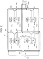
- FIG. 2 is a diagram for illustrating how an electric current flows when the semiconductor switching elements 102b and 102c are switched from an ON state to an OFF state in the single-phase inverter 102.
- the rectifier circuit 105 side is not illustrated.
- the semiconductor switching elements 102b and 102c are in the ON state, the electric current flows in the direction indicated by the solid line A, that is, in the order of the input capacitor 101, the semiconductor switching element 102c, the primary winding 104a of the transformer 104, the semiconductor switching element 102b, and the input capacitor 101.
- the electric current flows in the direction indicated by the dotted line B, that is, in the order of the transformer primary winding 104a, the control GND 112a, the inter-pattern parasitic capacitor 113, the control GND 112b, a drain-source parasitic capacitor of the semiconductor switching element 102b, and the transformer primary winding 104a.
- the inter-pattern parasitic capacitor 113 is charged.
- the charges thus accumulated in the inter-pattern parasitic capacitor 113 flow through the transformer primary winding 104a.
- the larger inter-pattern parasitic capacitor 113 causes a larger amount of current to flow through the transformer primary 104a side, and consequently causes a large loss on the transformer primary 104a side.
- the drain-source parasitic capacitors of the semiconductor switching elements 102a and 102d are discharged, and the drain-source parasitic capacitors of the semiconductor switching elements 102b and 102d are charged.
- those parasitic capacitors are small and thus are not illustrated.
- FIG. 3 is a diagram for illustrating how an electric current flows when the four semiconductor switching elements 102a to 102d are first in an OFF state and then, the two semiconductor switching elements 102a and 102d enter an ON state.
- the semiconductor switching elements 102a to 102d are in the OFF state, no electric current flows.
- the semiconductor switching elements 102a and 102d enter the ON state, an electric current flows in the direction indicated by the dotted line B, that is, in the order of the input capacitor 101, the semiconductor switching element 102a, the primary winding 104a of the transformer 104, the semiconductor switching element 102d, and the input capacitor 101.
- the electric current flows in the order of the input capacitor 101, the semiconductor switching element 102a, the control GND 112a, the inter-pattern parasitic capacitor 113, the control GND 112b, and the input capacitor 101.
- charges are accumulated in the inter-pattern parasitic capacitor 113.
- the charges thus accumulated flow through the semiconductor switching element 102a.
- the larger inter-pattern parasitic capacitor 113 causes a larger amount of current to flow through the semiconductor switching element 102a, and consequently causes a large loss on the semiconductor switching element 102a.
- the drain-source parasitic capacitors of the semiconductor switching elements 102a and 102d are discharged, and the drain-source parasitic capacitors of the semiconductor switching elements 102b and 102d are charged.
- those parasitic capacitors are small and thus are not illustrated.
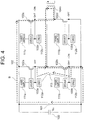
- FIG. 4 is a diagram for illustrating how an electric current flows when the four semiconductor switching elements 102a to 102d are first in an OFF state and then, the two semiconductor switching elements 102b and 102c enter an ON state.
- the semiconductor switching elements 102a to 102d are in the OFF state, no electric current flows.
- the semiconductor switching elements 102b and 102c enter the ON state, an electric current flows in the direction indicated by the dotted line B, that is, in the order of the input capacitor 101, the semiconductor switching element 102c, the primary winding 104a of the transformer 104, the semiconductor switching element 102b, and the input capacitor 101.
- the electric current flows in the order of the inter-pattern parasitic capacitor 113, the control GND 112a, the semiconductor switching element 102b, the control GND 112b, and the inter-pattern parasitic capacitor 113.
- the inter-pattern parasitic capacitor 113 causes a larger amount of current to flow through the semiconductor switching element 102b, and consequently causes a large loss on the semiconductor switching element 102b.
- the drain-source parasitic capacitors of the semiconductor switching elements 102a and 102d are charged, and the drain-source parasitic capacitors of the semiconductor switching elements 102b and 102d are discharged.
- those parasitic capacitors are small and thus are not illustrated.
- the inter-pattern parasitic capacitor 113 between the control GNDs 112a and 112b for different nodes is illustrated by way of example. However, the same applies to an inter-pattern parasitic capacitor between the control GNDs 112c and 112b for different nodes.
- FIG. 5 is a diagram for illustrating how an electric current flows when the four semiconductor switching elements 102a to 102d are first in an OFF state and then, the semiconductor switching elements 102b and 102c enter an ON state. When the semiconductor switching elements 102a to 102d are in the OFF state, no electric current flows.
- FIG. 6 is a diagram for illustrating how an electric current flows when the semiconductor switching elements 102b and 102c are switched from an ON state to an OFF state.
- the electric current flows in the direction indicated by the solid line A, that is, in the order of the input capacitor 101, the semiconductor switching element 102c, the primary winding 104a of the transformer 104, the semiconductor switching element 102b, and the input capacitor 101.
- the electric current flows in the direction indicated by the dotted line B, that is, in the order of the inter-pattern parasitic capacitor 114, the transformer primary winding 104a, the control GND 112a, and the inter-pattern parasitic capacitor 114. As a result, the charges of the inter-pattern parasitic capacitor 114 are released.
- the charges thus released flow through the transformer primary winding 104a.
- the semiconductor switching elements 102a to 102d are first in the OFF state and then, the semiconductor switching elements 102b and 102c enter the ON state and further the OFF state.
- the semiconductor switching elements 102a to 102d are first in an OFF state and then, the semiconductor switching elements 102a and 102d enter an ON state and further an OFF state, the inter-pattern parasitic capacitor 114 is charged/discharged as well.
- an electric current flows through each of the source wirings 211a to 211d (see FIG. 1 ) that connect the semiconductor switching elements 102a to 102d and the control GNDs of the drivers 103a to 103d, respectively, at a time of charging/discharging the inter-pattern parasitic capacitor 113 or the inter-pattern parasitic capacitor 114.
- a voltage drop occurs when the source wirings 211a to 211d have inductance.
- the voltage drop reflects on a gate voltage of each of the semiconductor switching elements 102a to 102d. There is a fear that the voltage drop leads to a noise on the gate voltage, and causes the semiconductor switching elements 102a to 102d to be unintentionally switched on or off, and eventually causes unstable operations thereof.
- the present invention it is possible to suppress an increase in loss of each of the semiconductor switching elements 102a to 102d, and the primary winding 104a of the transformer 104, and unstable operations of the semiconductor switching elements 102a to 102d, which may be caused by charging/discharging of the inter-pattern parasitic capacitor 113 or 114 as described above.
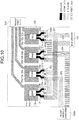
- FIG. 7 is a view for illustrating an example of the circuit board configuration of the power conversion circuit according to the first embodiment of the present invention.
- the following description is made of circuit board patterns for the plurality of control GNDs 112a to 112c for different nodes used to drive the semiconductor switching elements.
- FIG. 7 is a view for illustrating an example of patterns for the semiconductor switching elements 102a to 102d as components of the circuit of FIG. 1 , the drivers 103a to 103d for driving the semiconductor switching elements 102a to 102d, respectively, and the control GNDs 112a, 112b, and 112c to be connected to the drivers 103a to 103d, respectively.
- Identical or equivalent components to those of FIG. 1 are denoted by the same reference symbols.
- circuit patterns for the control power supplies 111a to 111c are illustrated as control power supply patterns 111a to 111c, respectively, and circuit patterns for the control GNDs 112a to 112c are illustrated as control GND patterns 112a to 112c, respectively.
- circuit patterns of first to fourth layers are illustrated as a solid pattern, a hatched pattern, a dot pattern, and a stripe pattern, respectively.
- the semiconductor switching elements 102a to 102d are inserted components having three lead terminals, that is, a drain (D), a gate (G), and a source (S).
- the drain terminal D of the semiconductor switching element 102a and the drain terminal D of the semiconductor switching element 102c are connected to a positive electrode of the input capacitor 101 via a circuit board pattern 201 in the third layer.
- the source terminal S of the semiconductor switching element 102b and the source terminal S of the semiconductor switching element 102d are connected to a negative electrode of the input capacitor 101 via a circuit board pattern 202 in the second layer.
- the source terminal S of the semiconductor switching element 102a and the drain terminal D of the semiconductor switching element 102b are connected to a first terminal of the transformer on the primary winding 104a side via a circuit board pattern 203 in the third layer. Further, the source terminal S of the semiconductor switching element 102c and the drain terminal D of the semiconductor switching element 102d are connected to a second terminal of the transformer on the primary winding 104a side via a circuit board pattern 204 in the fourth layer.
- the gates G of the semiconductor switching elements 102a to 102d are connected to the drivers 103a to 103d via gate wirings 210a to 210d as circuit board patterns, respectively. Further, the sources S of the semiconductor switching elements 102a to 102d are connected to the drivers 103a to 103d via the source wirings 211a to 211d as circuit board patterns, respectively.
- the isolated control GND patterns 112a to 112c are provided in the form of a solid pattern around the drivers 103a to 103d.
- the control GND patterns 112a to 112c are arranged so as not to overlap one another as seen in plan view from a stacking direction of the layers of the circuit board CB.
- the stacking direction of the layers of the circuit board CB refers to a direction orthogonal to the sheet of FIG. 7 .
- the control GND patterns 112a to 112c are connected to an isolated power supply 220 without overlapping one another.
- GND terminals (not shown) of the drivers 103a to 103d are connected to the control GND patterns 112a to 112c through vias, for example.
- the inter-pattern parasitic capacitors between the control GND 112a and the control GND 112b, between the control GND 112c and the control GND 112b, and between the control GND 112a and the control GND 112c can be reduced.
- this configuration it is possible to suppress an increase in loss of each of the semiconductor switching elements 102a to 102d and the primary winding 104a of the transformer, which may occur due to charging/discharging of any inter-pattern parasitic capacitor during switching operations of the semiconductor switching elements 102a to 102d.
- the isolated power supply 220 serves as the control power supplies 111a to 111c of FIG. 1 , which are configured to drive the drivers 103a to 103d corresponding to the control GND patterns 112a to 112c.
- the control power supply patterns 111a to 111c are wired so as to overlap the corresponding control GND patterns 112a to 112c, respectively, in different layers in the stacking direction of the layers of the circuit board CB.
- control GND pattern 112a is formed in the third layer
- the two control GND patterns 112b on both sides of the control GND pattern 112a are formed in the second layer
- control GND pattern 112c on the right side is formed in the fourth layer.
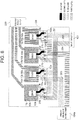
- FIG. 8 is a view for illustrating an example in which the control GND patterns of FIG. 7 are provided while being overlapped with suitable control power supply patterns.
- the control power supply pattern 111a is formed in the fourth layer (illustrated in a stripe pattern)
- the control power supply patterns 111b are formed in the third layer (illustrated in a dot pattern)
- the control power supply pattern 111c is formed in the third layer (illustrated in the dot pattern). Those patterns overlap the control GND patterns of FIG. 7 .
- the way to assign the wirings to the layers of the circuit board in the first embodiment is merely an example, and the present invention is not limited to the examples of FIG. 7 and FIG. 8 .
- the arrangement of the semiconductor switching elements 102a to 102d is merely an example, and the present invention is not limited to the examples above.
- the circuit board is a four-layer circuit board, but the number of layers is not limited thereto, and the circuit board may have six or more layers, for example.
- the semiconductor switching elements 102a to 102d are directly connected to the corresponding drivers 103a to 103d, respectively, but the semiconductor switching elements 102a to 102d can be connected to the corresponding drivers 103a to 103d, respectively, via resistors, capacitors, ferrite beads, or other such elements (not shown) interposed therebetween.
- the isolated GNDs for different nodes that is, the control power supply patterns are arranged so as not to overlap one another as seen in plan view from the stacking direction of the layers.
- the isolated GNDs for different nodes are wired in different positions in the same layer of the circuit board.
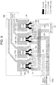
- FIG. 9 and FIG. 10 a pattern arrangement example in the second embodiment is described in detail.
- components of FIG. 9 and FIG. 10 which are the same as those of FIG. 7 and FIG. 8 , are denoted by the same reference symbols. The following description is focused on the differences from the configuration of FIG. 7 and FIG. 8 .
- a circuit configuration adopted herein is the same as that of FIG. 1 .
- the source wirings 211a to 211d and the circuit board patterns 202 and 203 that form power wirings to be connected to the source wirings are provided in the same layer. Further, the source wirings 211a to 211d and the control GND patterns 112a to 112c to be connected to the source wirings 211a to 211d are provided in the same layer.
- the source wirings 211a to 211d are all arranged in the same layer, for example, in the first layer.
- the control GND patterns 112a to 112c are arranged in different positions in the same layer, for example, in the second layer.
- GND terminals (not shown) of the drivers 103a to 103d are connected to the control GND patterns 112a to 112c through vias, for example.
- the inter-pattern parasitic capacitors between the control GND 112a and the control GND 112b, between the control GND 112c and the control GND 112b, and between the control GND 112a and the control GND 112c can be all reduced. It is accordingly possible to suppress an increase in loss of each of the semiconductor switching elements 102a to 102d and the primary winding 104a of the transformer, which may occur due to charging/discharging of any inter-pattern parasitic capacitor during the switching operations of the semiconductor switching elements 102a to 102d.
- the isolated power supply 220 serves as the control power supplies 111a to 111c of FIG. 1 , which are configured to drive the drivers 103a to 103d corresponding to the control GND patterns 112a to 112c.
- the control power supply patterns 111a to 111c are wired to the corresponding control GND patterns 112a to 112c, respectively, in a different layer therefrom, and are also arranged in different positions in the same layer, for example, in the third layer.
- control GND patterns 112a to 112c are arranged in different positions in the same layer, and the control power supply patterns 111a to 111c are arranged in different positions in the same layer.
- Such wiring patterns ensure an effect of reducing the inter-pattern parasitic capacitors and further, allow efficient use of a limited region of the circuit board to design circuit patterns. Hence, arrangement design of sensors or other such elements, or wirings can be made with ease, and the power conversion circuit board and the power conversion device can be downsized.
- a wiring pattern in which the control power supply patterns 111a to 111c are arranged so as to overlap the corresponding control GND patterns 112a to 112c, respectively, in the stacking direction of the layers of the circuit board CB may be adopted.
- control GND patterns 112a to 112c are all arranged in the same layer, but the present invention is not limited thereto. Some of the control GND patterns 112a to 112c may be formed in another wiring layer.
- the two control GND patterns 112b, 112b for the same node lie on each side of the control GND pattern 112a as a wiring for another node. Then, the two control GND patterns 112b, 112b thus physically separated from each other are connected to each other, for example, via a first layer wiring 310 and interlayer connection vias 301 formed at both ends of the first layer wiring 310.
- control GND patterns 112a to 112c in the same layer are for the same node but are physically separated from one another across any wiring for another node, those patterns are connected to each other via a wiring in another layer, with the result that the number of wirings to be connected to the isolated power supply 220 can be reduced.
- the power conversion circuit board can be downsized and consequently, the power conversion circuit and the power conversion device can be downsized.
- the way to assign the wirings to the layers of the circuit board in the second embodiment is merely an example, and the present invention is not limited thereto.
- the arrangement of the semiconductor switching elements 102a to 102d is also merely an example, and the present invention is not limited thereto.
- the circuit board is a four-layer circuit board, but the number of layers is not limited thereto, and the circuit board may have six or more layers, for example. Meanwhile, regarding two semiconductor switching elements that form one half-bridge circuit, it is also possible to achieve the power conversion circuit of the present invention with use of a two-layer circuit board.
- the control GND patterns (112a to 112c) are isolated from a housing of the power conversion circuit or the power conversion device. Further, in FIG. 7 to FIG. 11 , the isolated power supply 220, the primary winding 104a of the transformer, and the input capacitor 101 are provided outside the circuit board CB. However, those components may be mounted on the surface of the circuit board CB or in the circuit board CB together with the semiconductor switching elements 102a to 102d and the drivers 103a to 103d.
- the circuit patterns of the circuit board for the plurality of GNDs for different nodes which are used to drive the wide-bandgap semiconductor switching elements, are arranged so as not to overlap one another in plan view of the circuit board.
- the circuit patterns of the circuit board for the plurality of GNDs for different nodes are arranged in positions not overlapping each other in the stacking direction of the layers of the circuit board, or in different positions in the same layer.
- 100 input power supply 101 input capacitor, 102 single-phase inverter (power converter), 102a-102d semiconductor switching element, 103a-103d driver, 104 transformer, 104a primary winding, 104b secondary winding, 105 rectifier circuit, 105a-105d diode, 106 reactor, 107 output capacitor, 108 load, 109 control circuit, 110a-11 0f isolation element, 111a-111 c control power supply (control power supply pattern), 112a-112c control GND (control GND (ground) pattern), 113, 114 inter-pattern parasitic capacitor, 201-204 circuit board pattern (wiring), 210a gate wiring, 211a source wiring, 220 isolated power supply, 310 first layer wiring, CB circuit board
Landscapes
- Engineering & Computer Science (AREA)
- Power Engineering (AREA)
- Microelectronics & Electronic Packaging (AREA)
- Power Conversion In General (AREA)
- Dc-Dc Converters (AREA)
- Inverter Devices (AREA)
- Structures For Mounting Electric Components On Printed Circuit Boards (AREA)
- Structure Of Printed Boards (AREA)
Abstract
Description
- The present invention relates to a power conversion circuit for a power conversion device including a plurality of semiconductor switching elements, and more particularly, to a configuration of each of circuit board patterns for isolated circuits configured to drive the semiconductor switching elements.
- Power conversion devices often adopt a circuit of a half-bridge configuration, in which semiconductor switching elements are connected to each other in series. Drive circuits for the series-connected semiconductor switching elements are required to have different GNDs (reference potentials), and are achieved by, for example, isolated power supply circuits. In particular, in some uses that involve the application of several hundreds of volts, the respective circuits are required to be isolated from a housing, and a GND different from that of the housing is required as a GND for a semiconductor switching element of a lower arm in the half-bridge configuration. In a full-bridge configuration having two half-bridge configurations, a common GND can be used for semiconductor switching elements of lower arms of the two half-bridge configurations. However, different GNDs are required for semiconductor switching elements of upper arms thereof, with the result that the requisite number of GNDs for different nodes increases (see, for example,
Patent Literature 1 and Patent Literature 2). - In
Patent Literature 1, an inverter circuit has three half-bridge configurations including three upper-arm semiconductor switching elements, and three lower-arm semiconductor switching elements. Further, inPatent Literature 1, GNDs and power supplies for four different nodes in total are provided in the form of being isolated by optical means. - Likewise, in
Patent Literature 2, three half-bridge configurations are provided. Further, inPatent Literature 2, a bootstrapping configuration is employed for one of the half-bridge configurations of three inverter circuits, and hence a common power supply is used for driving circuits for semiconductor switching elements of upper and lower arms thereof. In other words, in the configuration ofPatent Literature 2, it is required to provide GNDs for every different node, and the inverter circuits are required to have GNDs for four different nodes in total. -
- [PTL 1]
JP 2013-208017 A - [PTL 2]
JP 2015-171237 A - However, the related art has the following problems.
- In general, a GND is formed with use of a solid pattern. The solid pattern is obtained by filling a large area. Thus, when there are a plurality of GNDs for different nodes, those GNDs for different nodes overlap one another in plan view, that is, as viewed from a direction orthogonal to a circuit board surface in many cases. Now, a consideration is made of a case of using a semiconductor switching element made of gallium nitride (GaN) or silicon carbide (SiC) having a wide bandgap. In this case, the wide-bandgap semiconductor has a feature of being capable of high-speed operation, and thus enables high-frequency switching. With this configuration, a power conversion device can be made compact by downsizing respective peripheral passive components.
- However, when a plurality of GNDs for different nodes overlap one another in plan view, parasitic capacitors are formed therebetween. For example, in a case where a GND used for driving a semiconductor switching element of a lower arm and a GND used for driving a semiconductor switching element of an upper arm in the half-bridge circuit overlap each other in plan view, a voltage between the GNDs overlapping in plan view varies depending on a switching period, and hence a parasitic capacitor therebetween is charged/discharged. In this case, charges are accumulated/released via any semiconductor switching element in an ON state, resulting in a problem of increasing a loss of the semiconductor switching element.
- Further, the semiconductor switching element having a wide bandgap achieves a high switching speed. This leads to a higher charging/discharging speed in parasitic capacitors between the plurality of GNDs for different nodes. Due to an influence of an electric current flowing during charging/discharging of each parasitic capacitor, a voltage drop occurs in a parasitic inductance portion of a GND wiring between a driver and a corresponding semiconductor switching element. This causes a problem that noise is superimposed on a gate of the semiconductor switching element, and the operation thereof becomes unstable.
- The present invention has been made to solve the problems described above, and an object of the present invention is generally to obtain a power conversion circuit for achieving a power conversion device capable of suppressing charging/discharging of a parasitic capacitor caused by high-frequency switching, and of reducing a loss of a semiconductor switching element that is not limited to a wide-bandgap semiconductor switching element.
- According to one embodiment of the present invention, there is provided a power conversion circuit including: a circuit board including a plurality of layers including two or more layers, on which circuit patterns are formed; and a plurality of semiconductor switching elements connected to the circuit patterns of the circuit board, and configured to perform switching for power conversion. In the circuit board, a plurality of control ground patterns for different nodes, which are configured to drive the plurality of semiconductor switching elements, are arranged so as not to overlap one another in plan view.
- According to the one embodiment of the present invention, the circuit patterns for the plurality of GNDs for different nodes used to drive the semiconductor switching elements are arranged so as not to overlap one another in plan view. With this configuration, it is possible to reduce the parasitic capacitors between the GNDs for different nodes, and thus to reduce a loss of each semiconductor switching element during high-frequency switching.
-
-
FIG. 1 is a circuit diagram for illustrating an example of a power conversion device including a power conversion circuit according to a first embodiment of the present invention. -
FIG. 2 is an explanatory diagram for illustrating a current path of a parasitic capacitor in the power conversion circuit according to the first embodiment of the present invention. -
FIG. 3 is an explanatory diagram for illustrating a current path of a parasitic capacitor in the power conversion circuit according to the first embodiment of the present invention. -
FIG. 4 is an explanatory diagram for illustrating a current path of a parasitic capacitor in the power conversion circuit according to the first embodiment of the present invention. -
FIG. 5 is an explanatory diagram for illustrating a current path of a parasitic capacitor in the power conversion circuit according to the first embodiment of the present invention. -
FIG. 6 is an explanatory diagram for illustrating a current path of a parasitic capacitor in the power conversion circuit according to the first embodiment of the present invention. -
FIG. 7 is a view for illustrating an example of a circuit pattern configuration, in particular, control GND patterns of a circuit board of the power conversion circuit according to the first embodiment of the present invention. -
FIG. 8 is a view for illustrating another example of the circuit pattern configuration, in particular, control GND patterns and control power supply patterns of the circuit board of the power conversion circuit according to the first embodiment of the present invention. -
FIG. 9 is a view for illustrating an example of a circuit pattern configuration, in particular, control GND patterns of a circuit board of a power conversion circuit according to a second embodiment of the present invention. -
FIG. 10 is a view for illustrating another example of the circuit pattern configuration, in particular, control GND patterns and control power supply patterns of the circuit board of the power conversion circuit according to the second embodiment of the present invention. -
FIG. 11 is a view for illustrating still another example of the circuit pattern configuration, in particular, control GND patterns of the circuit board of the power conversion circuit according to the second embodiment of the present invention. - Now, a power conversion circuit for a power conversion device according to each of embodiments of the present invention is described with reference to the drawings. In each of the embodiments, the same or corresponding portions are denoted by the same reference symbols, and the overlapping description thereof is omitted.
-
FIG. 1 is a circuit diagram for illustrating an example of a power conversion device including a power conversion circuit according to a first embodiment of the present invention. Referring toFIG. 1 , a description is given of a circuit board pattern having a plurality of control GNDs (control reference potentials) for different nodes used to drive semiconductor switching elements. In the following, the ground may also be referred to as "GND". - The illustrated example of the power conversion device of
FIG. 1 is an isolated full-bridge DC/DC converter, which includes a single-phase inverter 102 as a power converter, arectifier circuit 105, and atransformer 104 configured to connect the single-phase inverter 102 and therectifier circuit 105 to each other in an electrically isolated manner. - The single-
phase inverter 102 is an inverter connected in parallel to aninput power supply 100 and aninput capacitor 101, and is configured to convert a DC voltage Vin of theinput capacitor 101 to an AC voltage. The single-phase inverter 102 has a full-bridge configuration including foursemiconductor switching elements 102a to 102d (hereinafter simply referred to as "semiconductor switching elements") made of gallium nitride (GaN) having a reverse conduction characteristic in a source-drain direction. An output of the full-bridge single-phase inverter 102 is connected to aprimary winding 104a of thetransformer 104. - The
rectifier circuit 105 is connected to asecondary winding 104b of thetransformer 104. Further, therectifier circuit 105 has a full-bridge configuration including fourdiodes 105a to 105d as rectifier elements (semiconductor elements). Therectifier circuit 105 is series-connected, on its output side, to an output-smoothing reactor 106. Therectifier circuit 105 is also connected in parallel to anoutput capacitor 107. Further, a DC voltage across theoutput capacitor 107 is output as a DC voltage Vout to aload 108. - Further, a
control circuit 109 is provided outside a main circuit while being isolated therefrom. The input voltage Vin and the output voltage Vout are input to thecontrol circuit 109 viaisolation elements control circuit 109. Thecontrol circuit 109 outputs gate signals 110 to thesemiconductor switching elements 102a to 102d so as to obtain a target output voltage Vout, and thus controls on-duty (on period) of each of thesemiconductor switching elements 102a to 102d.Drivers 103a to 103d are connected to thesemiconductor switching elements 102a to 102d, respectively, to drive thesemiconductor switching elements 102a to 102d. Thedrivers 103a to 103d are connected to gates of thesemiconductor switching elements 102a to 102d viagate wirings 210a to 210d, respectively, and connected to sources of thesemiconductor switching elements 102a to 102d viasource wirings 211a to 211d, respectively. The gate signals 110 from thecontrol circuit 109 are input to thedrivers 103a to 103d viaisolation elements 110c to 110f, respectively. Thesemiconductor switching elements 102a to 102d may be semiconductor switching elements, each of which includes a diode connected in parallel between a source and a drain thereof, and is made of silicon carbide (SiC), a diamond-based material, or any material other than GaN. - Further, the
driver 103a is provided with a control power supply (1) 111a and a control GND (1) 112a. Thedriver 103b is provided with a control power supply (2) 111b and a control GND (2) 112b. Thedriver 103c is provided with a control power supply (3) 111c and a control GND (3) 112c. Isolation is established between the control power supply (1) 111a and the control GND (1) 112a, between the control power supply (2) 111b and the control GND (2) 112b, and between the control power supply (3) 111cand the control GND (3) 112c. - Meanwhile, the
driver 103d is configured to drive thesemiconductor switching element 102d having a source on the same node as a source of thesemiconductor switching element 102b, and is therefore provided with the same control power supply (2) 111b and the same control GND (2) 112b as those of thedriver 103b. - Next, referring to
FIG. 2 to FIG. 4 , a detailed description is given of an influence of any parasitic capacitor between control GNDs for different nodes in relation to a circuit operation ofFIG. 1 . The description is focused on an inter-patternparasitic capacitor 113 between thecontrol GNDs -
FIG. 2 is a diagram for illustrating how an electric current flows when thesemiconductor switching elements phase inverter 102. InFIG. 2 to FIG. 6 , therectifier circuit 105 side is not illustrated. When thesemiconductor switching elements input capacitor 101, thesemiconductor switching element 102c, the primary winding 104a of thetransformer 104, thesemiconductor switching element 102b, and theinput capacitor 101. - When the
semiconductor switching elements control GND 112a, the inter-patternparasitic capacitor 113, thecontrol GND 112b, a drain-source parasitic capacitor of thesemiconductor switching element 102b, and the transformer primary winding 104a. As a result, the inter-patternparasitic capacitor 113 is charged. The charges thus accumulated in the inter-patternparasitic capacitor 113 flow through the transformer primary winding 104a. This means that the larger inter-patternparasitic capacitor 113 causes a larger amount of current to flow through the transformer primary 104a side, and consequently causes a large loss on the transformer primary 104a side. - To describe exactly, when the
semiconductor switching elements semiconductor switching elements semiconductor switching elements -
FIG. 3 is a diagram for illustrating how an electric current flows when the foursemiconductor switching elements 102a to 102d are first in an OFF state and then, the twosemiconductor switching elements semiconductor switching elements 102a to 102d are in the OFF state, no electric current flows. When thesemiconductor switching elements input capacitor 101, thesemiconductor switching element 102a, the primary winding 104a of thetransformer 104, thesemiconductor switching element 102d, and theinput capacitor 101. To describe a current path of the parasitic capacitor, the electric current flows in the order of theinput capacitor 101, thesemiconductor switching element 102a, thecontrol GND 112a, the inter-patternparasitic capacitor 113, thecontrol GND 112b, and theinput capacitor 101. As a result, charges are accumulated in the inter-patternparasitic capacitor 113. The charges thus accumulated flow through thesemiconductor switching element 102a. This means that the larger inter-patternparasitic capacitor 113 causes a larger amount of current to flow through thesemiconductor switching element 102a, and consequently causes a large loss on thesemiconductor switching element 102a. - To describe exactly, when the
semiconductor switching elements semiconductor switching elements semiconductor switching elements -
FIG. 4 is a diagram for illustrating how an electric current flows when the foursemiconductor switching elements 102a to 102d are first in an OFF state and then, the twosemiconductor switching elements semiconductor switching elements 102a to 102d are in the OFF state, no electric current flows. When thesemiconductor switching elements input capacitor 101, thesemiconductor switching element 102c, the primary winding 104a of thetransformer 104, thesemiconductor switching element 102b, and theinput capacitor 101. To describe a current path of the parasitic capacitor, the electric current flows in the order of the inter-patternparasitic capacitor 113, thecontrol GND 112a, thesemiconductor switching element 102b, thecontrol GND 112b, and the inter-patternparasitic capacitor 113. As a result, charges are released from the inter-patternparasitic capacitor 113. The charges thus released flow through thesemiconductor switching element 102b. This means that the larger inter-patternparasitic capacitor 113 causes a larger amount of current to flow through thesemiconductor switching element 102b, and consequently causes a large loss on thesemiconductor switching element 102b. - To describe exactly, when the
semiconductor switching elements semiconductor switching elements semiconductor switching elements - In
FIG. 2 to FIG. 4 , the inter-patternparasitic capacitor 113 between thecontrol GNDs control GNDs - Next, referring to
FIG. 5 andFIG. 6 , a description is given of an influence of any parasitic capacitor between control GNDs for different nodes. Here, an inter-patternparasitic capacitor 114 between thecontrol GNDs FIG. 5 is a diagram for illustrating how an electric current flows when the foursemiconductor switching elements 102a to 102d are first in an OFF state and then, thesemiconductor switching elements semiconductor switching elements 102a to 102d are in the OFF state, no electric current flows. When thesemiconductor switching elements input capacitor 101, thesemiconductor switching element 102c, the primary winding 104a of thetransformer 104, thesemiconductor switching element 102b, and theinput capacitor 101. To describe a current path of the parasitic capacitor, the electric current flows in the order of theinput capacitor 101, thesemiconductor switching element 102c, thecontrol GND 112c, the inter-patternparasitic capacitor 114, thecontrol GND 112a, thesemiconductor switching element 102b, and theinput capacitor 101. As a result, the inter-patternparasitic capacitor 114 is charged. The charges thus accumulated flow through thesemiconductor switching elements parasitic capacitor 114 causes a larger amount of current to flow through thesemiconductor switching elements semiconductor switching elements -
FIG. 6 is a diagram for illustrating how an electric current flows when thesemiconductor switching elements semiconductor switching elements input capacitor 101, thesemiconductor switching element 102c, the primary winding 104a of thetransformer 104, thesemiconductor switching element 102b, and theinput capacitor 101. - When the
semiconductor switching elements parasitic capacitor 114, the transformer primary winding 104a, thecontrol GND 112a, and the inter-patternparasitic capacitor 114. As a result, the charges of the inter-patternparasitic capacitor 114 are released. - The charges thus released flow through the transformer primary winding 104a. This means that the larger inter-pattern
parasitic capacitor 114 causes a larger amount of current to flow through the transformer primary winding 104a, and consequently causes a large loss of the transformer primary winding 104a. - In the illustrated examples of
FIG. 5 andFIG. 6 , thesemiconductor switching elements 102a to 102d are first in the OFF state and then, thesemiconductor switching elements semiconductor switching elements 102a to 102d are first in an OFF state and then, thesemiconductor switching elements parasitic capacitor 114 is charged/discharged as well. - Further, in any of the illustrated examples of
FIG. 2 to FIG. 6 , an electric current flows through each of thesource wirings 211a to 211d (seeFIG. 1 ) that connect thesemiconductor switching elements 102a to 102d and the control GNDs of thedrivers 103a to 103d, respectively, at a time of charging/discharging the inter-patternparasitic capacitor 113 or the inter-patternparasitic capacitor 114. In this case, a voltage drop occurs when thesource wirings 211a to 211d have inductance. The voltage drop reflects on a gate voltage of each of thesemiconductor switching elements 102a to 102d. There is a fear that the voltage drop leads to a noise on the gate voltage, and causes thesemiconductor switching elements 102a to 102d to be unintentionally switched on or off, and eventually causes unstable operations thereof. - According to one embodiment of the present invention, it is possible to suppress an increase in loss of each of the
semiconductor switching elements 102a to 102d, and the primary winding 104a of thetransformer 104, and unstable operations of thesemiconductor switching elements 102a to 102d, which may be caused by charging/discharging of the inter-patternparasitic capacitor - Now, a description is given of a circuit board configuration of the power conversion circuit for the power conversion device according to the first embodiment of the present invention.
FIG. 7 is a view for illustrating an example of the circuit board configuration of the power conversion circuit according to the first embodiment of the present invention. The following description is made of circuit board patterns for the plurality ofcontrol GNDs 112a to 112c for different nodes used to drive the semiconductor switching elements. -
FIG. 7 is a view for illustrating an example of patterns for thesemiconductor switching elements 102a to 102d as components of the circuit ofFIG. 1 , thedrivers 103a to 103d for driving thesemiconductor switching elements 102a to 102d, respectively, and thecontrol GNDs drivers 103a to 103d, respectively. Identical or equivalent components to those ofFIG. 1 are denoted by the same reference symbols. - In
FIG. 7 to FIG. 11 , circuit patterns for thecontrol power supplies 111a to 111c are illustrated as controlpower supply patterns 111a to 111c, respectively, and circuit patterns for thecontrol GNDs 112a to 112c are illustrated ascontrol GND patterns 112a to 112c, respectively. Further, circuit patterns of first to fourth layers are illustrated as a solid pattern, a hatched pattern, a dot pattern, and a stripe pattern, respectively. - A circuit board CB having a plurality of layers including at least two or more layers, which is made of glass epoxy as a base material, has through-holes TH through which to mount the
semiconductor switching elements 102a to 102d. In this example, thesemiconductor switching elements 102a to 102d are inserted components having three lead terminals, that is, a drain (D), a gate (G), and a source (S). - The drain terminal D of the
semiconductor switching element 102a and the drain terminal D of thesemiconductor switching element 102c are connected to a positive electrode of theinput capacitor 101 via acircuit board pattern 201 in the third layer. The source terminal S of thesemiconductor switching element 102b and the source terminal S of thesemiconductor switching element 102d are connected to a negative electrode of theinput capacitor 101 via acircuit board pattern 202 in the second layer. - Further, the source terminal S of the
semiconductor switching element 102a and the drain terminal D of thesemiconductor switching element 102b are connected to a first terminal of the transformer on the primary winding 104a side via acircuit board pattern 203 in the third layer. Further, the source terminal S of thesemiconductor switching element 102c and the drain terminal D of thesemiconductor switching element 102d are connected to a second terminal of the transformer on the primary winding 104a side via acircuit board pattern 204 in the fourth layer. - The gates G of the
semiconductor switching elements 102a to 102d are connected to thedrivers 103a to 103d viagate wirings 210a to 210d as circuit board patterns, respectively. Further, the sources S of thesemiconductor switching elements 102a to 102d are connected to thedrivers 103a to 103d via thesource wirings 211a to 211d as circuit board patterns, respectively. - The isolated
control GND patterns 112a to 112c are provided in the form of a solid pattern around thedrivers 103a to 103d. Thecontrol GND patterns 112a to 112c are arranged so as not to overlap one another as seen in plan view from a stacking direction of the layers of the circuit board CB. The stacking direction of the layers of the circuit board CB refers to a direction orthogonal to the sheet ofFIG. 7 . Thecontrol GND patterns 112a to 112c are connected to anisolated power supply 220 without overlapping one another. GND terminals (not shown) of thedrivers 103a to 103d are connected to thecontrol GND patterns 112a to 112c through vias, for example. - By thus arranging the
control GND patterns 112a to 112c for different nodes so as not to overlap one another as seen in plan view from the stacking direction of the layers, the inter-pattern parasitic capacitors between thecontrol GND 112a and thecontrol GND 112b, between thecontrol GND 112c and thecontrol GND 112b, and between thecontrol GND 112a and thecontrol GND 112c can be reduced. With this configuration, it is possible to suppress an increase in loss of each of thesemiconductor switching elements 102a to 102d and the primary winding 104a of the transformer, which may occur due to charging/discharging of any inter-pattern parasitic capacitor during switching operations of thesemiconductor switching elements 102a to 102d. It is also possible to reduce an electric current that flows through thesource wirings 211a to 211d due to charging/discharging of any inter-pattern parasitic capacitor during the switching operations of thesemiconductor switching elements 102a to 102d. This configuration can prevent such a situation that noise is superimposed on the gates of thesemiconductor switching elements 102a to 102d, to thereby cause the respective elements to operate unstably, and thus can ensure stable operations of thesemiconductor switching elements 102a to 102d. - The
isolated power supply 220 serves as thecontrol power supplies 111a to 111c ofFIG. 1 , which are configured to drive thedrivers 103a to 103d corresponding to thecontrol GND patterns 112a to 112c. As illustrated inFIG. 8 , the controlpower supply patterns 111a to 111c are wired so as to overlap the correspondingcontrol GND patterns 112a to 112c, respectively, in different layers in the stacking direction of the layers of the circuit board CB. By thus wiring thecontrol GND patterns 112a to 112c and the controlpower supply patterns 111a to 111c, inter-pattern parasitic capacitors are formed between those wiring pairs, to thereby achieve a more stable power supply. - In
FIG. 7 , thecontrol GND pattern 112a is formed in the third layer, the twocontrol GND patterns 112b on both sides of thecontrol GND pattern 112a are formed in the second layer, and thecontrol GND pattern 112c on the right side is formed in the fourth layer. -
FIG. 8 is a view for illustrating an example in which the control GND patterns ofFIG. 7 are provided while being overlapped with suitable control power supply patterns. The controlpower supply pattern 111a is formed in the fourth layer (illustrated in a stripe pattern), the controlpower supply patterns 111b are formed in the third layer (illustrated in a dot pattern), and the controlpower supply pattern 111c is formed in the third layer (illustrated in the dot pattern). Those patterns overlap the control GND patterns ofFIG. 7 . - The way to assign the wirings to the layers of the circuit board in the first embodiment is merely an example, and the present invention is not limited to the examples of
FIG. 7 andFIG. 8 . Further, the arrangement of thesemiconductor switching elements 102a to 102d is merely an example, and the present invention is not limited to the examples above. Furthermore, in the example described in the first embodiment, the circuit board is a four-layer circuit board, but the number of layers is not limited thereto, and the circuit board may have six or more layers, for example. - In the example described in the first embodiment, the
semiconductor switching elements 102a to 102d are directly connected to the correspondingdrivers 103a to 103d, respectively, but thesemiconductor switching elements 102a to 102d can be connected to the correspondingdrivers 103a to 103d, respectively, via resistors, capacitors, ferrite beads, or other such elements (not shown) interposed therebetween. - Now, a second embodiment of the present invention is described.
- In the example described in the first embodiment, the isolated GNDs for different nodes, that is, the control power supply patterns are arranged so as not to overlap one another as seen in plan view from the stacking direction of the layers. In contrast, in the second embodiment, there is described an example in which the isolated GNDs for different nodes are wired in different positions in the same layer of the circuit board. Referring to
FIG. 9 andFIG. 10 , a pattern arrangement example in the second embodiment is described in detail. Here, components ofFIG. 9 andFIG. 10 , which are the same as those ofFIG. 7 andFIG. 8 , are denoted by the same reference symbols. The following description is focused on the differences from the configuration ofFIG. 7 andFIG. 8 . A circuit configuration adopted herein is the same as that ofFIG. 1 . - In the first embodiment, the
source wirings 211a to 211d and thecircuit board patterns source wirings 211a to 211d and thecontrol GND patterns 112a to 112c to be connected to thesource wirings 211a to 211d are provided in the same layer. In the second embodiment, as illustrated inFIG. 9 , thesource wirings 211a to 211d are all arranged in the same layer, for example, in the first layer. Further, thecontrol GND patterns 112a to 112c are arranged in different positions in the same layer, for example, in the second layer. Here, GND terminals (not shown) of thedrivers 103a to 103d are connected to thecontrol GND patterns 112a to 112c through vias, for example. - By thus arranging the
control GND patterns 112a to 112c for different nodes in the same layer of the circuit board, the inter-pattern parasitic capacitors between thecontrol GND 112a and thecontrol GND 112b, between thecontrol GND 112c and thecontrol GND 112b, and between thecontrol GND 112a and thecontrol GND 112c can be all reduced. It is accordingly possible to suppress an increase in loss of each of thesemiconductor switching elements 102a to 102d and the primary winding 104a of the transformer, which may occur due to charging/discharging of any inter-pattern parasitic capacitor during the switching operations of thesemiconductor switching elements 102a to 102d. Further, it is also possible to reduce an electric current that flows through thesource wirings 211a to 211d due to charging/discharging of any inter-pattern parasitic capacitor during the switching operations of thesemiconductor switching elements 102a to 102d. This configuration can prevent such a situation that noise is superimposed on the gates of, to thereby cause the elements to operate unstably, and thus can ensure stable operations of thesemiconductor switching elements 102a to 102d. - The
isolated power supply 220 serves as thecontrol power supplies 111a to 111c ofFIG. 1 , which are configured to drive thedrivers 103a to 103d corresponding to thecontrol GND patterns 112a to 112c. As illustrated inFIG. 10 , the controlpower supply patterns 111a to 111c are wired to the correspondingcontrol GND patterns 112a to 112c, respectively, in a different layer therefrom, and are also arranged in different positions in the same layer, for example, in the third layer. - As described above, in the wiring patterns adopted in the second embodiment, the
control GND patterns 112a to 112c are arranged in different positions in the same layer, and the controlpower supply patterns 111a to 111c are arranged in different positions in the same layer. Such wiring patterns ensure an effect of reducing the inter-pattern parasitic capacitors and further, allow efficient use of a limited region of the circuit board to design circuit patterns. Hence, arrangement design of sensors or other such elements, or wirings can be made with ease, and the power conversion circuit board and the power conversion device can be downsized. Further, as an alternative, a wiring pattern in which the controlpower supply patterns 111a to 111c are arranged so as to overlap the correspondingcontrol GND patterns 112a to 112c, respectively, in the stacking direction of the layers of the circuit board CB may be adopted. By thus wiring thecontrol GND patterns 112a to 112c and the controlpower supply patterns 111a to 111c, inter-pattern parasitic capacitors are formed between those wiring pairs, to thereby achieve a more stable power supply. - In the illustrated example of
FIG. 9 , thecontrol GND patterns 112a to 112c are all arranged in the same layer, but the present invention is not limited thereto. Some of thecontrol GND patterns 112a to 112c may be formed in another wiring layer. InFIG. 11 , the twocontrol GND patterns control GND pattern 112a as a wiring for another node. Then, the twocontrol GND patterns first layer wiring 310 and interlayer connection vias 301 formed at both ends of thefirst layer wiring 310. - When some of the
control GND patterns 112a to 112c in the same layer are for the same node but are physically separated from one another across any wiring for another node, those patterns are connected to each other via a wiring in another layer, with the result that the number of wirings to be connected to theisolated power supply 220 can be reduced. With this configuration, the power conversion circuit board can be downsized and consequently, the power conversion circuit and the power conversion device can be downsized. - The way to assign the wirings to the layers of the circuit board in the second embodiment is merely an example, and the present invention is not limited thereto. The arrangement of the
semiconductor switching elements 102a to 102d is also merely an example, and the present invention is not limited thereto. Further, in the example described in the second embodiment, the circuit board is a four-layer circuit board, but the number of layers is not limited thereto, and the circuit board may have six or more layers, for example. Meanwhile, regarding two semiconductor switching elements that form one half-bridge circuit, it is also possible to achieve the power conversion circuit of the present invention with use of a two-layer circuit board. - Regarding a power conversion circuit designed for use with a high voltage, the control GND patterns (112a to 112c) are isolated from a housing of the power conversion circuit or the power conversion device. Further, in
FIG. 7 to FIG. 11 , theisolated power supply 220, the primary winding 104a of the transformer, and theinput capacitor 101 are provided outside the circuit board CB. However, those components may be mounted on the surface of the circuit board CB or in the circuit board CB together with thesemiconductor switching elements 102a to 102d and thedrivers 103a to 103d. - According to one embodiment of the present invention, the circuit patterns of the circuit board for the plurality of GNDs for different nodes, which are used to drive the wide-bandgap semiconductor switching elements, are arranged so as not to overlap one another in plan view of the circuit board. Specifically, the circuit patterns of the circuit board for the plurality of GNDs for different nodes are arranged in positions not overlapping each other in the stacking direction of the layers of the circuit board, or in different positions in the same layer. With this configuration, it is possible to reduce the parasitic capacitors between the GNDs for different nodes, and reduce a loss of each semiconductor switching element during a high-frequency switching operation, and consequently to improve an efficiency of the power conversion circuit, and reduce a size and cost of the power conversion circuit by simplifying a cooling structure for each semiconductor switching element. Further, it is also possible to reduce an electric current flowing through a parasitic inductance portion of a GND wiring between a driver and a semiconductor switching element during a high-speed switching operation, and consequently to achieve a stable high-speed switching operation.
- 100 input power supply, 101 input capacitor, 102 single-phase inverter (power converter), 102a-102d semiconductor switching element, 103a-103d driver, 104 transformer, 104a primary winding, 104b secondary winding, 105 rectifier circuit, 105a-105d diode, 106 reactor, 107 output capacitor, 108 load, 109 control circuit, 110a-11 0f isolation element, 111a-111 c control power supply (control power supply pattern), 112a-112c control GND (control GND (ground) pattern), 113, 114 inter-pattern parasitic capacitor, 201-204 circuit board pattern (wiring), 210a gate wiring, 211a source wiring, 220 isolated power supply, 310 first layer wiring, CB circuit board
Claims (10)
- A power conversion circuit, comprising:a circuit board including a plurality of layers including two or more layers, on which circuit patterns are formed; anda plurality of semiconductor switching elements, which are connected to the circuit patterns of the circuit board, and are configured to perform switching for power conversion,wherein, in the circuit board, a plurality of control ground patterns for different nodes, which are configured to drive the plurality of semiconductor switching elements, are arranged so as not to overlap one another in plan view.
- The power conversion circuit according to claim 1, wherein the plurality of semiconductor switching elements are each formed of a wide-bandgap semiconductor.
- The power conversion circuit according to claim 1 or 2, further comprising:at least one half-bridge circuit including the plurality of semiconductor switching elements;a first control ground pattern, which is connected to a source of a first semiconductor switching element that forms the at least one half-bridge circuit, and is connected to a ground of a driver configured to drive the first semiconductor switching element; anda second control ground pattern, which is connected to a source of a second semiconductor switching element that forms the at least one half-bridge circuit, the source being different from the source of the first semiconductor switching element, and is connected to a ground of a driver configured to drive the second semiconductor switching element,wherein the first control ground pattern and the second control ground pattern are provided in positions not overlapping each other in a stacking direction of the plurality of layers of the circuit board.
- The power conversion circuit according to claim 1 or 2, further comprising:at least one half-bridge circuit including the plurality of semiconductor switching elements;a first control ground pattern, which is connected to a source of a first semiconductor switching element that forms the at least one half-bridge circuit, and is connected to a ground of a driver configured to drive the first semiconductor switching element; anda second control ground pattern, which is connected to a source of a second semiconductor switching element that forms the at least one half-bridge circuit, the source being different from the source of the first semiconductor switching element, and is connected to a ground of a driver configured to drive the second semiconductor switching element,wherein the first control ground pattern and the second control ground pattern are provided in different positions in the same layer of the circuit board.
- The power conversion circuit according to claim 3 or 4, wherein a first control power supply pattern using the first control ground pattern as a reference and a second control power supply pattern using the second control ground pattern as a reference are arranged in different positions in the same layer of the circuit board.
- The power conversion circuit according to any one of claims 3 to 5, wherein the first control ground pattern and the second control ground pattern are isolated from a housing of the power conversion circuit.
- The power conversion circuit according to claim 5, wherein the first control ground pattern and the first control power supply pattern are provided in positions overlapping each other in the stacking direction of the plurality of layers of the circuit board, and the second control ground pattern and the second control power supply pattern are provided in positions overlapping each other in the stacking direction of the plurality of layers of the circuit board.
- The power conversion circuit according to any one of claims 3 to 7, wherein the first semiconductor switching element and the second semiconductor switching element are semiconductor switching elements of an upper arm and a lower arm, which form one half-bridge circuit.
- The power conversion circuit according to any one of claims 3 to 7,
wherein the power conversion circuit includes a plurality of the half-bridge circuits, and
wherein the first semiconductor switching element and the second semiconductor switching element are semiconductor switching elements of upper arms of different half-bridge circuits. - The power conversion circuit according to any one of claims 1 to 9,
wherein the plurality of semiconductor switching elements are semiconductor switching elements made of GaN.
Applications Claiming Priority (2)
| Application Number | Priority Date | Filing Date | Title |
|---|---|---|---|
| JP2017193583A JP6549200B2 (en) | 2017-10-03 | 2017-10-03 | Power conversion circuit |
| PCT/JP2018/015097 WO2019069489A1 (en) | 2017-10-03 | 2018-04-10 | Power conversion circuit |
Publications (3)
| Publication Number | Publication Date |
|---|---|
| EP3694093A1 true EP3694093A1 (en) | 2020-08-12 |
| EP3694093A4 EP3694093A4 (en) | 2020-10-28 |
| EP3694093B1 EP3694093B1 (en) | 2024-05-08 |
Family
ID=65994569
Family Applications (1)
| Application Number | Title | Priority Date | Filing Date |
|---|---|---|---|
| EP18864523.8A Active EP3694093B1 (en) | 2017-10-03 | 2018-04-10 | Power conversion circuit |
Country Status (5)
| Country | Link |
|---|---|
| US (1) | US11336188B2 (en) |
| EP (1) | EP3694093B1 (en) |
| JP (1) | JP6549200B2 (en) |
| CN (1) | CN111133666B (en) |
| WO (1) | WO2019069489A1 (en) |
Cited By (1)
| Publication number | Priority date | Publication date | Assignee | Title |
|---|---|---|---|---|
| US12184191B2 (en) | 2020-09-17 | 2024-12-31 | Rohm Co., Ltd. | Power conversion device |
Families Citing this family (5)
| Publication number | Priority date | Publication date | Assignee | Title |
|---|---|---|---|---|
| US12119756B2 (en) | 2020-04-20 | 2024-10-15 | Hitachi Industrial Equipment Systems Co., Ltd. | Power conversion device |
| CN113346752B (en) * | 2020-07-03 | 2025-02-18 | 广东工业大学 | An isolated high-frequency dual active bridge converter based on GaN devices |
| WO2022071472A1 (en) * | 2020-09-30 | 2022-04-07 | ダイキン工業株式会社 | Power conversion device |
| JP7203141B2 (en) * | 2021-04-15 | 2023-01-12 | 三菱電機株式会社 | power converter |
| EP4449828A4 (en) * | 2021-12-17 | 2025-04-09 | Exro Technologies Inc. | ARTICLES FOR AN INVERTER AND INVERTER |
Family Cites Families (25)
| Publication number | Priority date | Publication date | Assignee | Title |
|---|---|---|---|---|
| JP2854757B2 (en) * | 1992-06-17 | 1999-02-03 | 三菱電機株式会社 | Semiconductor power module |
| JP2003199327A (en) * | 2001-12-28 | 2003-07-11 | Yaskawa Electric Corp | Gate drive circuit of power converter |
| US6859087B2 (en) * | 2002-10-31 | 2005-02-22 | International Rectifier Corporation | Half-bridge high voltage gate driver providing protection of a transistor |
| KR100799856B1 (en) * | 2005-07-07 | 2008-01-31 | 삼성전기주식회사 | High efficiency half-bridge DC / DC converter and control method thereof |
| WO2007049788A1 (en) * | 2005-10-28 | 2007-05-03 | Hitachi Metals, Ltd. | Dc-dc converter |
| JP4793225B2 (en) * | 2006-11-07 | 2011-10-12 | 株式会社デンソー | Inverter device |
| JP5029900B2 (en) * | 2007-11-20 | 2012-09-19 | アイシン・エィ・ダブリュ株式会社 | Motor control device |
| JP5444619B2 (en) * | 2008-02-07 | 2014-03-19 | 株式会社ジェイテクト | Multi-layer circuit board and motor drive circuit board |
| JP5422663B2 (en) * | 2009-10-22 | 2014-02-19 | パナソニック株式会社 | Power semiconductor module |
| WO2011096164A1 (en) * | 2010-02-03 | 2011-08-11 | 本田技研工業株式会社 | Semiconductor device |
| JP5599260B2 (en) | 2010-08-11 | 2014-10-01 | 株式会社東芝 | High frequency switch |
| JP2012186784A (en) * | 2010-12-24 | 2012-09-27 | Renesas Electronics Corp | Crystal oscillation device and semiconductor device |
| CN102545560B (en) * | 2011-12-15 | 2014-09-03 | 无锡中星微电子有限公司 | Power switch driver, IC chip, and DC-DC converter |
| JP5810896B2 (en) * | 2011-12-22 | 2015-11-11 | 株式会社ソシオネクスト | DC-DC converter and control method of DC-DC converter |
| JP2013208017A (en) | 2012-03-29 | 2013-10-07 | Denso Corp | Power conversion device |
| JP5845428B2 (en) * | 2013-08-22 | 2016-01-20 | パナソニックIpマネジメント株式会社 | Drive device, power conversion device, vehicle |
| JP6303129B2 (en) | 2014-03-07 | 2018-04-04 | パナソニックIpマネジメント株式会社 | Motor drive device |
| JP2015154591A (en) * | 2014-02-14 | 2015-08-24 | ローム株式会社 | Gate drive circuit and power supply device |
| JP6421484B2 (en) * | 2014-07-28 | 2018-11-14 | Tdk株式会社 | Coil parts, coil parts composite and transformer, and power supply device |
| JP6237554B2 (en) | 2014-09-24 | 2017-11-29 | アイシン・エィ・ダブリュ株式会社 | Power conversion device control board |
| JP6327113B2 (en) * | 2014-10-30 | 2018-05-23 | 株式会社明電舎 | Power converter |
| MX359050B (en) | 2014-12-03 | 2018-09-13 | Nissan Motor | Power conversion device. |
| EP4096085A1 (en) * | 2015-03-24 | 2022-11-30 | Mitsubishi Electric Corporation | Power conversion device |
| US11075589B2 (en) * | 2019-05-20 | 2021-07-27 | Ford Global Technologies, Llc | DC inverter/converter current balancing for paralleled phase leg switches |
| CN113228265B (en) * | 2019-07-03 | 2024-09-24 | 富士电机株式会社 | Circuit structure of semiconductor components |
-
2017
- 2017-10-03 JP JP2017193583A patent/JP6549200B2/en active Active
-
2018
- 2018-04-10 CN CN201880061227.3A patent/CN111133666B/en active Active
- 2018-04-10 EP EP18864523.8A patent/EP3694093B1/en active Active
- 2018-04-10 US US16/639,978 patent/US11336188B2/en active Active
- 2018-04-10 WO PCT/JP2018/015097 patent/WO2019069489A1/en not_active Ceased
Cited By (1)
| Publication number | Priority date | Publication date | Assignee | Title |
|---|---|---|---|---|
| US12184191B2 (en) | 2020-09-17 | 2024-12-31 | Rohm Co., Ltd. | Power conversion device |
Also Published As
| Publication number | Publication date |
|---|---|
| US20210376740A1 (en) | 2021-12-02 |
| JP6549200B2 (en) | 2019-07-24 |
| WO2019069489A1 (en) | 2019-04-11 |
| CN111133666B (en) | 2024-03-29 |
| EP3694093B1 (en) | 2024-05-08 |
| CN111133666A (en) | 2020-05-08 |
| US11336188B2 (en) | 2022-05-17 |
| EP3694093A4 (en) | 2020-10-28 |
| JP2019068664A (en) | 2019-04-25 |
Similar Documents
| Publication | Publication Date | Title |
|---|---|---|
| EP3694093B1 (en) | Power conversion circuit | |
| US7697306B2 (en) | DC/DC converter | |
| CN101286694B (en) | DC/DC power conversion device | |
| US9979314B2 (en) | Power semiconductor module and power conversion device | |
| CN102214644B (en) | Power semiconductor device and power conversion system using the device | |
| US7619907B2 (en) | DC/DC power conversion device | |
| US12563670B2 (en) | Power converter device and a system comprising the same | |
| US11626790B2 (en) | Power conversion device minimizing footprint | |
| US10620654B2 (en) | Alternatingly-switched parallel circuit, integrated power module and integrated power package | |
| JP6184507B2 (en) | Driver board and power conversion device | |
| US10985645B2 (en) | Alternatingly-switched parallel circuit, integrated power module and integrated power package | |
| US10198020B2 (en) | Interleaved parallel circuit, integrated power module and integrated power chip | |
| JPWO2008075418A1 (en) | 3-level power converter | |
| US11710685B2 (en) | Semiconductor module and power conversion device | |
| US20190363636A1 (en) | DC/DC Converter with Full-Bridge Actuation | |
| JP2015211581A (en) | Full bridge DC / DC converter | |
| WO2013136623A1 (en) | Power converter and apparatus for controlling same | |
| JP6851242B2 (en) | Power converter | |
| EP2575245A2 (en) | Integrated switching power supply device and electric apparatus | |
| CN112910234A (en) | Boost converter and method for operating a boost converter | |
| US12525887B2 (en) | Power converter | |
| JP6451591B2 (en) | Power converter | |
| US20260031717A1 (en) | Multi-phase power converter circuit layout to minimize drive loop and power loop inductances | |
| JP6440772B2 (en) | Power converter | |
| JP6624643B2 (en) | Semiconductor module and power conversion device using the module |
Legal Events
| Date | Code | Title | Description |
|---|---|---|---|
| STAA | Information on the status of an ep patent application or granted ep patent |
Free format text: STATUS: THE INTERNATIONAL PUBLICATION HAS BEEN MADE |
|
| PUAI | Public reference made under article 153(3) epc to a published international application that has entered the european phase |
Free format text: ORIGINAL CODE: 0009012 |
|
| STAA | Information on the status of an ep patent application or granted ep patent |
Free format text: STATUS: REQUEST FOR EXAMINATION WAS MADE |
|
| 17P | Request for examination filed |
Effective date: 20200218 |
|
| AK | Designated contracting states |
Kind code of ref document: A1 Designated state(s): AL AT BE BG CH CY CZ DE DK EE ES FI FR GB GR HR HU IE IS IT LI LT LU LV MC MK MT NL NO PL PT RO RS SE SI SK SM TR |
|
| AX | Request for extension of the european patent |
Extension state: BA ME |
|
| REG | Reference to a national code |
Ref country code: DE Ref legal event code: R079 Free format text: PREVIOUS MAIN CLASS: H02M0003280000 Ipc: H02M0003335000 Ref document number: 602018069364 Country of ref document: DE |
|
| A4 | Supplementary search report drawn up and despatched |
Effective date: 20200928 |
|
| RIC1 | Information provided on ipc code assigned before grant |
Ipc: H02M 3/335 20060101AFI20200922BHEP Ipc: H02M 1/096 20060101ALI20200922BHEP Ipc: H02M 1/00 20060101ALI20200922BHEP Ipc: H03K 17/689 20060101ALI20200922BHEP Ipc: H02M 1/08 20060101ALI20200922BHEP Ipc: H02M 7/00 20060101ALI20200922BHEP Ipc: H05K 9/00 20060101ALI20200922BHEP Ipc: H05K 1/02 20060101ALI20200922BHEP |
|
| DAV | Request for validation of the european patent (deleted) | ||
| DAX | Request for extension of the european patent (deleted) | ||
| STAA | Information on the status of an ep patent application or granted ep patent |
Free format text: STATUS: EXAMINATION IS IN PROGRESS |
|
| 17Q | First examination report despatched |
Effective date: 20220215 |
|
| GRAP | Despatch of communication of intention to grant a patent |
Free format text: ORIGINAL CODE: EPIDOSNIGR1 |
|
| STAA | Information on the status of an ep patent application or granted ep patent |
Free format text: STATUS: GRANT OF PATENT IS INTENDED |
|
| INTG | Intention to grant announced |
Effective date: 20231212 |
|
| GRAS | Grant fee paid |
Free format text: ORIGINAL CODE: EPIDOSNIGR3 |
|
| GRAA | (expected) grant |
Free format text: ORIGINAL CODE: 0009210 |
|
| STAA | Information on the status of an ep patent application or granted ep patent |
Free format text: STATUS: THE PATENT HAS BEEN GRANTED |
|
| AK | Designated contracting states |
Kind code of ref document: B1 Designated state(s): AL AT BE BG CH CY CZ DE DK EE ES FI FR GB GR HR HU IE IS IT LI LT LU LV MC MK MT NL NO PL PT RO RS SE SI SK SM TR |
|
| REG | Reference to a national code |
Ref country code: GB Ref legal event code: FG4D |
|
| REG | Reference to a national code |
Ref country code: CH Ref legal event code: EP |
|
| REG | Reference to a national code |
Ref country code: DE Ref legal event code: R096 Ref document number: 602018069364 Country of ref document: DE |
|
| REG | Reference to a national code |
Ref country code: IE Ref legal event code: FG4D |
|
| REG | Reference to a national code |
Ref country code: LT Ref legal event code: MG9D |
|
| REG | Reference to a national code |
Ref country code: NL Ref legal event code: MP Effective date: 20240508 |
|
| PG25 | Lapsed in a contracting state [announced via postgrant information from national office to epo] |
Ref country code: IS Free format text: LAPSE BECAUSE OF FAILURE TO SUBMIT A TRANSLATION OF THE DESCRIPTION OR TO PAY THE FEE WITHIN THE PRESCRIBED TIME-LIMIT Effective date: 20240908 |
|
| PG25 | Lapsed in a contracting state [announced via postgrant information from national office to epo] |
Ref country code: BG Free format text: LAPSE BECAUSE OF FAILURE TO SUBMIT A TRANSLATION OF THE DESCRIPTION OR TO PAY THE FEE WITHIN THE PRESCRIBED TIME-LIMIT Effective date: 20240508 |
|
| PG25 | Lapsed in a contracting state [announced via postgrant information from national office to epo] |
Ref country code: HR Free format text: LAPSE BECAUSE OF FAILURE TO SUBMIT A TRANSLATION OF THE DESCRIPTION OR TO PAY THE FEE WITHIN THE PRESCRIBED TIME-LIMIT Effective date: 20240508 Ref country code: FI Free format text: LAPSE BECAUSE OF FAILURE TO SUBMIT A TRANSLATION OF THE DESCRIPTION OR TO PAY THE FEE WITHIN THE PRESCRIBED TIME-LIMIT Effective date: 20240508 |
|
| PG25 | Lapsed in a contracting state [announced via postgrant information from national office to epo] |
Ref country code: GR Free format text: LAPSE BECAUSE OF FAILURE TO SUBMIT A TRANSLATION OF THE DESCRIPTION OR TO PAY THE FEE WITHIN THE PRESCRIBED TIME-LIMIT Effective date: 20240809 |
|
| PG25 | Lapsed in a contracting state [announced via postgrant information from national office to epo] |
Ref country code: PT Free format text: LAPSE BECAUSE OF FAILURE TO SUBMIT A TRANSLATION OF THE DESCRIPTION OR TO PAY THE FEE WITHIN THE PRESCRIBED TIME-LIMIT Effective date: 20240909 |
|
| REG | Reference to a national code |
Ref country code: AT Ref legal event code: MK05 Ref document number: 1685836 Country of ref document: AT Kind code of ref document: T Effective date: 20240508 |
|
| PG25 | Lapsed in a contracting state [announced via postgrant information from national office to epo] |
Ref country code: NL Free format text: LAPSE BECAUSE OF FAILURE TO SUBMIT A TRANSLATION OF THE DESCRIPTION OR TO PAY THE FEE WITHIN THE PRESCRIBED TIME-LIMIT Effective date: 20240508 |
|
| PG25 | Lapsed in a contracting state [announced via postgrant information from national office to epo] |
Ref country code: ES Free format text: LAPSE BECAUSE OF FAILURE TO SUBMIT A TRANSLATION OF THE DESCRIPTION OR TO PAY THE FEE WITHIN THE PRESCRIBED TIME-LIMIT Effective date: 20240508 |
|
| PG25 | Lapsed in a contracting state [announced via postgrant information from national office to epo] |
Ref country code: AT Free format text: LAPSE BECAUSE OF FAILURE TO SUBMIT A TRANSLATION OF THE DESCRIPTION OR TO PAY THE FEE WITHIN THE PRESCRIBED TIME-LIMIT Effective date: 20240508 |
|
| PG25 | Lapsed in a contracting state [announced via postgrant information from national office to epo] |
Ref country code: PL Free format text: LAPSE BECAUSE OF FAILURE TO SUBMIT A TRANSLATION OF THE DESCRIPTION OR TO PAY THE FEE WITHIN THE PRESCRIBED TIME-LIMIT Effective date: 20240508 |
|
| PG25 | Lapsed in a contracting state [announced via postgrant information from national office to epo] |
Ref country code: LV Free format text: LAPSE BECAUSE OF FAILURE TO SUBMIT A TRANSLATION OF THE DESCRIPTION OR TO PAY THE FEE WITHIN THE PRESCRIBED TIME-LIMIT Effective date: 20240508 |
|
| PG25 | Lapsed in a contracting state [announced via postgrant information from national office to epo] |
Ref country code: PT Free format text: LAPSE BECAUSE OF FAILURE TO SUBMIT A TRANSLATION OF THE DESCRIPTION OR TO PAY THE FEE WITHIN THE PRESCRIBED TIME-LIMIT Effective date: 20240909 Ref country code: PL Free format text: LAPSE BECAUSE OF FAILURE TO SUBMIT A TRANSLATION OF THE DESCRIPTION OR TO PAY THE FEE WITHIN THE PRESCRIBED TIME-LIMIT Effective date: 20240508 Ref country code: NO Free format text: LAPSE BECAUSE OF FAILURE TO SUBMIT A TRANSLATION OF THE DESCRIPTION OR TO PAY THE FEE WITHIN THE PRESCRIBED TIME-LIMIT Effective date: 20240808 Ref country code: NL Free format text: LAPSE BECAUSE OF FAILURE TO SUBMIT A TRANSLATION OF THE DESCRIPTION OR TO PAY THE FEE WITHIN THE PRESCRIBED TIME-LIMIT Effective date: 20240508 Ref country code: LV Free format text: LAPSE BECAUSE OF FAILURE TO SUBMIT A TRANSLATION OF THE DESCRIPTION OR TO PAY THE FEE WITHIN THE PRESCRIBED TIME-LIMIT Effective date: 20240508 Ref country code: IS Free format text: LAPSE BECAUSE OF FAILURE TO SUBMIT A TRANSLATION OF THE DESCRIPTION OR TO PAY THE FEE WITHIN THE PRESCRIBED TIME-LIMIT Effective date: 20240908 Ref country code: HR Free format text: LAPSE BECAUSE OF FAILURE TO SUBMIT A TRANSLATION OF THE DESCRIPTION OR TO PAY THE FEE WITHIN THE PRESCRIBED TIME-LIMIT Effective date: 20240508 Ref country code: GR Free format text: LAPSE BECAUSE OF FAILURE TO SUBMIT A TRANSLATION OF THE DESCRIPTION OR TO PAY THE FEE WITHIN THE PRESCRIBED TIME-LIMIT Effective date: 20240809 Ref country code: FI Free format text: LAPSE BECAUSE OF FAILURE TO SUBMIT A TRANSLATION OF THE DESCRIPTION OR TO PAY THE FEE WITHIN THE PRESCRIBED TIME-LIMIT Effective date: 20240508 Ref country code: ES Free format text: LAPSE BECAUSE OF FAILURE TO SUBMIT A TRANSLATION OF THE DESCRIPTION OR TO PAY THE FEE WITHIN THE PRESCRIBED TIME-LIMIT Effective date: 20240508 Ref country code: BG Free format text: LAPSE BECAUSE OF FAILURE TO SUBMIT A TRANSLATION OF THE DESCRIPTION OR TO PAY THE FEE WITHIN THE PRESCRIBED TIME-LIMIT Effective date: 20240508 Ref country code: AT Free format text: LAPSE BECAUSE OF FAILURE TO SUBMIT A TRANSLATION OF THE DESCRIPTION OR TO PAY THE FEE WITHIN THE PRESCRIBED TIME-LIMIT Effective date: 20240508 Ref country code: RS Free format text: LAPSE BECAUSE OF FAILURE TO SUBMIT A TRANSLATION OF THE DESCRIPTION OR TO PAY THE FEE WITHIN THE PRESCRIBED TIME-LIMIT Effective date: 20240808 |
|
| PG25 | Lapsed in a contracting state [announced via postgrant information from national office to epo] |
Ref country code: DK Free format text: LAPSE BECAUSE OF FAILURE TO SUBMIT A TRANSLATION OF THE DESCRIPTION OR TO PAY THE FEE WITHIN THE PRESCRIBED TIME-LIMIT Effective date: 20240508 |
|
| PG25 | Lapsed in a contracting state [announced via postgrant information from national office to epo] |
Ref country code: EE Free format text: LAPSE BECAUSE OF FAILURE TO SUBMIT A TRANSLATION OF THE DESCRIPTION OR TO PAY THE FEE WITHIN THE PRESCRIBED TIME-LIMIT Effective date: 20240508 |
|
| PG25 | Lapsed in a contracting state [announced via postgrant information from national office to epo] |
Ref country code: CZ Free format text: LAPSE BECAUSE OF FAILURE TO SUBMIT A TRANSLATION OF THE DESCRIPTION OR TO PAY THE FEE WITHIN THE PRESCRIBED TIME-LIMIT Effective date: 20240508 |
|
| PG25 | Lapsed in a contracting state [announced via postgrant information from national office to epo] |
Ref country code: SK Free format text: LAPSE BECAUSE OF FAILURE TO SUBMIT A TRANSLATION OF THE DESCRIPTION OR TO PAY THE FEE WITHIN THE PRESCRIBED TIME-LIMIT Effective date: 20240508 Ref country code: RO Free format text: LAPSE BECAUSE OF FAILURE TO SUBMIT A TRANSLATION OF THE DESCRIPTION OR TO PAY THE FEE WITHIN THE PRESCRIBED TIME-LIMIT Effective date: 20240508 |
|
| PG25 | Lapsed in a contracting state [announced via postgrant information from national office to epo] |
Ref country code: SM Free format text: LAPSE BECAUSE OF FAILURE TO SUBMIT A TRANSLATION OF THE DESCRIPTION OR TO PAY THE FEE WITHIN THE PRESCRIBED TIME-LIMIT Effective date: 20240508 |
|
| PG25 | Lapsed in a contracting state [announced via postgrant information from national office to epo] |
Ref country code: SM Free format text: LAPSE BECAUSE OF FAILURE TO SUBMIT A TRANSLATION OF THE DESCRIPTION OR TO PAY THE FEE WITHIN THE PRESCRIBED TIME-LIMIT Effective date: 20240508 Ref country code: SK Free format text: LAPSE BECAUSE OF FAILURE TO SUBMIT A TRANSLATION OF THE DESCRIPTION OR TO PAY THE FEE WITHIN THE PRESCRIBED TIME-LIMIT Effective date: 20240508 Ref country code: RO Free format text: LAPSE BECAUSE OF FAILURE TO SUBMIT A TRANSLATION OF THE DESCRIPTION OR TO PAY THE FEE WITHIN THE PRESCRIBED TIME-LIMIT Effective date: 20240508 Ref country code: EE Free format text: LAPSE BECAUSE OF FAILURE TO SUBMIT A TRANSLATION OF THE DESCRIPTION OR TO PAY THE FEE WITHIN THE PRESCRIBED TIME-LIMIT Effective date: 20240508 Ref country code: DK Free format text: LAPSE BECAUSE OF FAILURE TO SUBMIT A TRANSLATION OF THE DESCRIPTION OR TO PAY THE FEE WITHIN THE PRESCRIBED TIME-LIMIT Effective date: 20240508 Ref country code: CZ Free format text: LAPSE BECAUSE OF FAILURE TO SUBMIT A TRANSLATION OF THE DESCRIPTION OR TO PAY THE FEE WITHIN THE PRESCRIBED TIME-LIMIT Effective date: 20240508 |
|
| PG25 | Lapsed in a contracting state [announced via postgrant information from national office to epo] |
Ref country code: IT Free format text: LAPSE BECAUSE OF FAILURE TO SUBMIT A TRANSLATION OF THE DESCRIPTION OR TO PAY THE FEE WITHIN THE PRESCRIBED TIME-LIMIT Effective date: 20240508 |
|
| REG | Reference to a national code |
Ref country code: DE Ref legal event code: R097 Ref document number: 602018069364 Country of ref document: DE |
|
| PLBE | No opposition filed within time limit |
Free format text: ORIGINAL CODE: 0009261 |
|
| STAA | Information on the status of an ep patent application or granted ep patent |
Free format text: STATUS: NO OPPOSITION FILED WITHIN TIME LIMIT |
|
| 26N | No opposition filed |
Effective date: 20250211 |
|
| PG25 | Lapsed in a contracting state [announced via postgrant information from national office to epo] |
Ref country code: SI Free format text: LAPSE BECAUSE OF FAILURE TO SUBMIT A TRANSLATION OF THE DESCRIPTION OR TO PAY THE FEE WITHIN THE PRESCRIBED TIME-LIMIT Effective date: 20240508 |
|
| PGFP | Annual fee paid to national office [announced via postgrant information from national office to epo] |
Ref country code: FR Payment date: 20250310 Year of fee payment: 8 |
|
| PGFP | Annual fee paid to national office [announced via postgrant information from national office to epo] |
Ref country code: DE Payment date: 20250305 Year of fee payment: 8 |
|
| PG25 | Lapsed in a contracting state [announced via postgrant information from national office to epo] |
Ref country code: SE Free format text: LAPSE BECAUSE OF FAILURE TO SUBMIT A TRANSLATION OF THE DESCRIPTION OR TO PAY THE FEE WITHIN THE PRESCRIBED TIME-LIMIT Effective date: 20240508 |
|
| REG | Reference to a national code |
Ref country code: CH Ref legal event code: H13 Free format text: ST27 STATUS EVENT CODE: U-0-0-H10-H13 (AS PROVIDED BY THE NATIONAL OFFICE) Effective date: 20251125 |
|
| PG25 | Lapsed in a contracting state [announced via postgrant information from national office to epo] |
Ref country code: LU Free format text: LAPSE BECAUSE OF NON-PAYMENT OF DUE FEES Effective date: 20250410 |
|
| PG25 | Lapsed in a contracting state [announced via postgrant information from national office to epo] |
Ref country code: MC Free format text: LAPSE BECAUSE OF FAILURE TO SUBMIT A TRANSLATION OF THE DESCRIPTION OR TO PAY THE FEE WITHIN THE PRESCRIBED TIME-LIMIT Effective date: 20240508 |
|
| GBPC | Gb: european patent ceased through non-payment of renewal fee |
Effective date: 20250410 |
|
| REG | Reference to a national code |
Ref country code: BE Ref legal event code: MM Effective date: 20250430 |
|
| PG25 | Lapsed in a contracting state [announced via postgrant information from national office to epo] |
Ref country code: GB Free format text: LAPSE BECAUSE OF NON-PAYMENT OF DUE FEES Effective date: 20250410 |
|
| PG25 | Lapsed in a contracting state [announced via postgrant information from national office to epo] |
Ref country code: BE Free format text: LAPSE BECAUSE OF NON-PAYMENT OF DUE FEES Effective date: 20250430 |
|
| PG25 | Lapsed in a contracting state [announced via postgrant information from national office to epo] |
Ref country code: CH Free format text: LAPSE BECAUSE OF NON-PAYMENT OF DUE FEES Effective date: 20250430 |
|
| PG25 | Lapsed in a contracting state [announced via postgrant information from national office to epo] |
Ref country code: IE Free format text: LAPSE BECAUSE OF NON-PAYMENT OF DUE FEES Effective date: 20250410 |