JP6851242B2 - Power converter - Google Patents
Power converter Download PDFInfo
- Publication number
- JP6851242B2 JP6851242B2 JP2017076718A JP2017076718A JP6851242B2 JP 6851242 B2 JP6851242 B2 JP 6851242B2 JP 2017076718 A JP2017076718 A JP 2017076718A JP 2017076718 A JP2017076718 A JP 2017076718A JP 6851242 B2 JP6851242 B2 JP 6851242B2
- Authority
- JP
- Japan
- Prior art keywords
- power
- circuit board
- printed circuit
- power module
- semiconductor switching
- Prior art date
- Legal status (The legal status is an assumption and is not a legal conclusion. Google has not performed a legal analysis and makes no representation as to the accuracy of the status listed.)
- Active
Links
Images


Classifications
-
- Y—GENERAL TAGGING OF NEW TECHNOLOGICAL DEVELOPMENTS; GENERAL TAGGING OF CROSS-SECTIONAL TECHNOLOGIES SPANNING OVER SEVERAL SECTIONS OF THE IPC; TECHNICAL SUBJECTS COVERED BY FORMER USPC CROSS-REFERENCE ART COLLECTIONS [XRACs] AND DIGESTS
- Y02—TECHNOLOGIES OR APPLICATIONS FOR MITIGATION OR ADAPTATION AGAINST CLIMATE CHANGE
- Y02E—REDUCTION OF GREENHOUSE GAS [GHG] EMISSIONS, RELATED TO ENERGY GENERATION, TRANSMISSION OR DISTRIBUTION
- Y02E10/00—Energy generation through renewable energy sources
- Y02E10/50—Photovoltaic [PV] energy
- Y02E10/56—Power conversion systems, e.g. maximum power point trackers
Description
本発明は、半導体スイッチング素子と半導体スイッチング素子の駆動回路とを同一パッケージに組み込んだ複数のパワーモジュールが配置されるプリント基板を備える電力変換装置に関する。 The present invention relates to a power conversion device including a printed circuit board on which a plurality of power modules in which a semiconductor switching element and a drive circuit of the semiconductor switching element are incorporated in the same package are arranged.
従来のインバータ又はコンバータの半導体スイッチング素子にはシリコン半導体が使用されていたが、近年では、炭化ケイ素(Silicon Carbide:SiC)及び窒化ガリウム(Gallium Nitride:GaN)といったワイドバンドギャップ半導体の使用が注目されている。ワイドバンドギャップ半導体で構成される半導体スイッチング素子ではスイッチ動作時の電圧変化速度及び電流変化速度が速いため、従来では問題にならなかった電力変換装置の構成部品間の配線インダクタンス又は配線相互間の寄生容量に起因するサージ電圧の発生が無視できなくなってきている。 Silicon semiconductors have been used for semiconductor switching elements of conventional inverters or converters, but in recent years, the use of wide bandgap semiconductors such as silicon carbide (SiC) and gallium nitride (GaN) has attracted attention. ing. In semiconductor switching elements composed of wideband gap semiconductors, the voltage change rate and current change rate during switch operation are high, so wiring inductance between wiring inductance or wiring between wiring, which has not been a problem in the past, has not been a problem in the past. The generation of surge voltage due to capacitance cannot be ignored.
特許文献1に開示される電力変換装置は、正極導体板及び負極導体板が絶縁シートを介して積層される3層積層構造の積層配線板と、インバータ回路を構成する2つのパワーモジュールと、複数のコンデンサとを備え、2つのパワーモジュールが並列に配置され、複数のコンデンサのそれぞれの正極端子が正極導体板に接続され、複数のコンデンサのそれぞれの負極端子が負極導体板に接続されている。特許文献1に開示される電力変換装置は、複数のコンデンサからパワーモジュールまでの電力配線に積層構造の配線を採用することにより、複数のコンデンサからパワーモジュールまでの配線インピーダンスを同等の値にできる。これにより配線インダクタンスのバラツキに起因して生じるパワーモジュールのサージ電圧を低減している。
The power conversion device disclosed in
しかしながら、特許文献1に開示されるように、平滑コンデンサから半導体素子に至る複数の電流経路のそれぞれの配線インピーダンスが同等の値であっても、ワイドバンドギャップ半導体で構成される半導体スイッチング素子が高速駆動されると、当該電流経路に流れる電流の変化が早い。そのため、配線インピーダンスの両端に発生するサージ電圧が大きくなり、サージ電圧の発生による半導体素子の故障又は電波雑音の増加が問題となる。また、複数の半導体スイッチング素子を1パッケージ化したパワーモジュールを複数使用して機器を構成する場合には、回路全体の面積が増加するため、電流経路が大きくなり電流経路のインピーダンスが大きくなるという課題がある。
However, as disclosed in
本発明は、上記に鑑みてなされたものであって、サージ電圧の発生による半導体素子の故障又は電波雑音の増加を抑制できる電力変換装置を得ることを目的とする。 The present invention has been made in view of the above, and an object of the present invention is to obtain a power conversion device capable of suppressing a failure of a semiconductor element or an increase in radio wave noise due to the generation of a surge voltage.
上述した課題を解決し、目的を達成するために、本発明の電力変換装置は、プリント基板と、プリント基板に設けられる複数のパワーモジュールと、プリント基板に設けられるスナバコンデンサと、プリント基板に設けられる平滑コンデンサとを備え、パワーモジュールは、半導体スイッチング素子を有するパッケージと、パッケージに設けられた電力側端子と、パッケージに設けられた制御側端子とを備え、電力側端子からスナバコンデンサまでの距離は、制御側端子からスナバコンデンサまでの距離よりも短く、プリント基板は、複数の配線レイヤを有し、平滑コンデンサの正側と負側の端子は、複数の配線レイヤにおいて互いに異なるレイヤを使用して互いに配線されると共に、電力側端子に配線される。パワーモジュールは、直列接続された2つの半導体スイッチング素子の半導体スイッチング素子対を複数備え、複数の半導体スイッチング素子対のそれぞれの一端が平滑コンデンサの正側に接続され、複数の前記半導体スイッチング素子対のそれぞれの他端が平滑コンデンサの負側に接続され、電力側端子は、直列接続された2つの半導体スイッチング素子の接続点に接続される出力端子を備える。複数の半導体スイッチング素子対のそれぞれを構成する2つの半導スイッチング素子の接続点に接続される出力端子が相互に接続され、複数の半導体スイッチング素子対の内、平滑コンデンサの正側に接続された複数の半導体スイッチング素子を同じタイミングでオン/オフ駆動し、複数の半導体スイッチング素子対の内、平滑コンデンサの負側に接続された複数の半導体スイッチング素子を同じタイミングでオン/オフ駆動する。 In order to solve the above-mentioned problems and achieve the object, the power conversion device of the present invention is provided on the printed circuit board, a plurality of power modules provided on the printed circuit board, a snubber capacitor provided on the printed circuit board, and the printed circuit board. The power module includes a package having a semiconductor switching element, a power side terminal provided in the package, and a control side terminal provided in the package, and the distance from the power side terminal to the snubber capacitor. Is shorter than the distance from the control side terminal to the snubber capacitor, the printed circuit board has multiple wiring layers, and the positive and negative terminals of the smoothing capacitor use different layers in the multiple wiring layers. together are wired together Te, Ru is wired to the power-side terminal. The power module includes a plurality of semiconductor switching element pairs of two semiconductor switching elements connected in series, one end of each of the plurality of semiconductor switching element pairs is connected to the positive side of the smoothing capacitor, and the plurality of semiconductor switching element pairs The other end of each is connected to the negative side of the smoothing capacitor, and the power side terminal includes an output terminal connected to the connection point of two semiconductor switching elements connected in series. The output terminals connected to the connection points of the two semiconducting switching elements constituting each of the plurality of semiconductor switching element pairs were connected to each other, and were connected to the positive side of the smoothing capacitor among the plurality of semiconductor switching element pairs. A plurality of semiconductor switching elements are driven on / off at the same timing, and among a plurality of semiconductor switching element pairs, a plurality of semiconductor switching elements connected to the negative side of the smoothing capacitor are driven on / off at the same timing.
本発明によれば、サージ電圧の発生による半導体素子の故障又は電波雑音の増加を抑制できる、という効果を奏する。 According to the present invention, it is possible to suppress a failure of a semiconductor element or an increase in radio wave noise due to the generation of a surge voltage.
以下に、本発明の実施の形態に係る電力変換装置を図面に基づいて詳細に説明する。なお、この実施の形態によりこの発明が限定されるものではない。 Hereinafter, the power conversion device according to the embodiment of the present invention will be described in detail with reference to the drawings. The present invention is not limited to this embodiment.
実施の形態1.
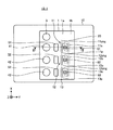
図1は実施の形態1に係る電力変換装置が備えるプリント基板とプリント基板に設けられる部品群とを示す図である。図2は図1に示すII−II矢視断面図である。図3は実施の形態1に係る電力変換装置が備える電力変換回路の構成例を示す図である。図4は図3に示すパワーモジュールの構成例を示す図である。
FIG. 1 is a diagram showing a printed circuit board included in the power conversion device according to the first embodiment and a group of parts provided on the printed circuit board. FIG. 2 is a cross-sectional view taken along the line II-II shown in FIG. FIG. 3 is a diagram showing a configuration example of a power conversion circuit included in the power conversion device according to the first embodiment. FIG. 4 is a diagram showing a configuration example of the power module shown in FIG.
図1に示すように実施の形態1に係る電力変換装置10−1は、電力変換装置10−1の外郭を構成する筐体10と、筐体10の内部に設けられるプリント基板1を備える。プリント基板1は、3つのパワーモジュール11,12,13と、入力コンデンサ3と、3つの平滑コンデンサ41,42,43と、3つのスナバコンデンサ51,52,53と、3つの出力端子61,62,63とを備える。
As shown in FIG. 1, the power conversion device 10-1 according to the first embodiment includes a
図1では、プリント基板1上において3つのパワーモジュール11,12,13の配列方向をX軸方向とし、プリント基板1上においてX軸方向と直交する方向をY軸方向とし、X軸方向とY軸方向の両者に直交する方向をZ軸方向とする。Z軸方向はプリント基板1の厚み方向、すなわちプリント基板1の一方の板面から他方の板面に向かう方向に等しい。
In FIG. 1, the arrangement direction of the three
以下では、3つのパワーモジュール11,12,13を「パワーモジュール11,12,13」と称し、3つの平滑コンデンサ41,42,43を「平滑コンデンサ41,42,43」と称し、3つのスナバコンデンサ51,52,53を「スナバコンデンサ51,52,53」と称し、3つの出力端子61,62,63を「出力端子61,62,63」と称する場合がある。
In the following, the three
図1では、プリント基板1に設けられるパワーモジュール11,12,13が3つの例を示しているが、実施の形態1に係る電力変換装置10−1を構成するパワーモジュールの数は、3つに限定されず、2つ以上であればよい。図1では、プリント基板1に設けられる平滑コンデンサ41,42,43が3つの例を示しているが、実施の形態1に係る電力変換装置10−1を構成する平滑コンデンサの数は、3つに限定されず、1つ以上であればよい。図1では、プリント基板1に設けられるスナバコンデンサ51,52,53が3つの例を示しているが、実施の形態1に係る電力変換装置10−1を構成するスナバコンデンサの数は、3つに限定されず、1つ以上であればよい。
In FIG. 1, the
図1に示すパワーモジュール11は、複数の半導体スイッチング素子及びスイッチ駆動回路を備えたパッケージ11pkgと、電力側端子11pと、制御側端子11sとを備える。パワーモジュール12は、複数の半導体スイッチング素子及びスイッチ駆動回路を備えたパッケージ12pkgと、電力側端子12pと、制御側端子12sとを備える。パワーモジュール13は、複数の半導体スイッチング素子及びスイッチ駆動回路を備えたパッケージ13pkgと、電力側端子13pと、制御側端子13sとを備える。
The
図2に示すようにプリント基板1には符号1a,1bで示す2つの配線レイヤがあり、2つの配線レイヤにはそれぞれ異なる配線パターンが形成されている。符号1aで示す第1の配線パターンは、プリント基板1のZ軸方向の一方の板面上に形成されている。符号1bで示す第2の配線パターンは、プリント基板1のZ軸方向の他方の板面上に形成されている。図1では、プリント基板1の第1の配線パターン1a側に設けられた部品が実線で示され、プリント基板1の第2の配線パターン1b側に設けられた部品が点線で示される。プリント基板1の第1の配線パターン1a側には、入力コンデンサ3と、平滑コンデンサ41,42,43と、スナバコンデンサ51,52,53と、出力端子61,62,63とが設けられている。プリント基板1の第2の配線パターン1b側には、パワーモジュール11,12,13が設けられている。
As shown in FIG. 2, the printed
図1に示すようにパワーモジュール11,12,13は、X軸方向にパワーモジュール11、パワーモジュール12及びパワーモジュール13の順で互いに離間して設けられている。平滑コンデンサ41,42,43は、X軸方向に平滑コンデンサ41、平滑コンデンサ42及び平滑コンデンサ43の順で互いに離間して設けられている。スナバコンデンサ51,52,53は、X軸方向にスナバコンデンサ51、スナバコンデンサ52及びスナバコンデンサ53の順で互いに離間して設けられている。
As shown in FIG. 1, the
平滑コンデンサ41、スナバコンデンサ51及びパワーモジュール11は、Y軸方向に平滑コンデンサ41、スナバコンデンサ51及びパワーモジュール11の順で互いに離間して設けられている。スナバコンデンサ51は、パワーモジュール11と平滑コンデンサ41との間に設けられている。パワーモジュール11のパッケージ11pkgとスナバコンデンサ51との間には、電力側端子11pが設けられている。パワーモジュール11の制御側端子11sは、パワーモジュール11のY軸方向の電力側端子11pとは反対側に設けられている。プリント基板1のXY平面内において、パワーモジュール11の電力側端子11pからスナバコンデンサ51までの距離は、パワーモジュール11の電力側端子11pから平滑コンデンサ41までの距離よりも短い。
The
平滑コンデンサ42、スナバコンデンサ52及びパワーモジュール12は、Y軸方向に平滑コンデンサ42、スナバコンデンサ52及びパワーモジュール12の順で互いに離間して設けられている。スナバコンデンサ52は、パワーモジュール12と平滑コンデンサ42との間に設けられている。パワーモジュール12のパッケージ12pkgとスナバコンデンサ52との間には、電力側端子12pが設けられている。パワーモジュール12の制御側端子12sは、パワーモジュール12のY軸方向の電力側端子12pとは反対側に設けられている。プリント基板1のXY平面内において、パワーモジュール12の電力側端子12pからスナバコンデンサ52までの距離は、パワーモジュール12の電力側端子12pから平滑コンデンサ42までの距離よりも短い。
The smoothing
平滑コンデンサ43、スナバコンデンサ53及びパワーモジュール13は、Y軸方向に平滑コンデンサ43、スナバコンデンサ53及びパワーモジュール13の順で互いに離間して設けられている。スナバコンデンサ53は、パワーモジュール13と平滑コンデンサ43との間に設けられている。パワーモジュール13のパッケージ13pkgとスナバコンデンサ53との間には、電力側端子13pが設けられている。パワーモジュール13の制御側端子13sは、パワーモジュール13のY軸方向の電力側端子13pとは反対側に設けられている。プリント基板1のXY平面内において、パワーモジュール13の電力側端子13pからスナバコンデンサ53までの距離は、パワーモジュール13の電力側端子13pから平滑コンデンサ43までの距離よりも短い。
The smoothing
図1に示すように、一列に配列されるパワーモジュール11,12,13は、一列に配列される平滑コンデンサ41,42,43と平行に設けられ、一列に配列されるパワーモジュール11,12,13のそれぞれの電力側端子11p,12p,13pは、一直線上に配列されている。具体的には、電力側端子11p、電力側端子12p及び電力側端子13pは、図1に示す仮想線20上に配列されると共に、互いに離間して配列されている。仮想線20は、プリント基板1のXY平面内においてX軸方向に伸びる仮想的な直線である。このように一列に配列される電力側端子11p、電力側端子12p及び電力側端子13pの近くには、スナバコンデンサ51,52,53と平滑コンデンサ41,42,43とが設けられている。そして、電力側端子11p,12p,13pからスナバコンデンサ51,52,53までの距離が、電力側端子11p,12p,13pから平滑コンデンサ41,42,43までの距離よりも短くなるように、パワーモジュール11,12,13とスナバコンデンサ51,52,53と平滑コンデンサ41,42,43とがプリント基板1上に配列されている。
As shown in FIG. 1, the
図2に示すように、出力端子61は、プリント基板1の第1の配線パターン1a側に配置され、パワーモジュール11は、プリント基板1の第2の配線パターン1b側に配置される。出力端子61は、パワーモジュール11をZ軸方向へプリント基板1に向かって投影してなる領域11A内に設けられている。なお図1に示す出力端子62は、パワーモジュール12をZ軸方向へプリント基板1に向かって投影してなる領域内に設けられている。また出力端子63は、パワーモジュール13をZ軸方向へプリント基板1に向かって投影してなる領域内に設けられている。
As shown in FIG. 2, the
図2に示すように、出力端子61には、ねじ101によりリード線102が取り付けられる。リード線102は、図3に示す直流電力入力部8に接続される。出力端子61に設けられた端子61aは、プリント基板1に形成された不図示のスルーホールに挿入され、例えば第2の配線パターン1bに半田付けされる。パワーモジュール11の電力側端子11pは、不図示のスルーホールに挿入されて、例えば第2の配線パターン1bに半田付けされる。出力端子61の端子61aとパワーモジュール11の電力側端子11pとは、第2の配線パターン1bにより電気的に接続される。
As shown in FIG. 2, a
図2に示すように、パワーモジュール11をZ軸方向へプリント基板1に向かって投影してなる領域11A内に出力端子61が設けられることにより、パワーモジュール11の電力側端子11pから出力端子61の端子61aに至るプリント基板1上の配線パターンを、電力側端子11pのスナバコンデンサ51側へ迂回させることなく配線できる。以下では、パワーモジュール11の電力側端子11pから出力端子61の端子61aに至るプリント基板1上の配線パターンを「第1の基板配線パターン」と称する。
As shown in FIG. 2, by providing the
第1の基板配線パターンを電力側端子11pのスナバコンデンサ51側へ迂回させた場合、第1の基板配線パターンは、スナバコンデンサ51及び平滑コンデンサ41の周囲に設けられる不図示の複数の配線パターン間に配線しなければならず、第1の基板配線パターンの配線幅を広げることができないという制約が生じる。以下では、スナバコンデンサ51及び平滑コンデンサ41の周囲に設けられる不図示の配線パターンを「第2の基板配線パターン」と称する。第2の基板配線パターンは、例えば、平滑コンデンサ41から電力側端子11pに至る配線パターンや、スナバコンデンサ51から電力側端子11pに至る配線パターンである。図2に示す位置に出力端子61を設けることにより、第1の基板配線パターンを複数の第2の基板配線パターン間に配線する必要がなくなり、第1の基板配線パターンの配線幅を広げることができる。
When the first board wiring pattern is bypassed to the
図3に示すように電力変換装置10−1は、直流電圧を特定の値の直流電圧に変換して出力するコンバータ110と、コンバータ110が出力する直流電圧を特定の値の交流電圧に変換して出力するインバータ120と、パワーモジュール11,12,13の各々が有する複数の半導体スイッチング素子のオンオフ動作を制御するためのパルス幅変調(Pulse Width Modulation:PWM)信号を生成する制御部130とを備える。直流電源7は、例えば、電力変換装置10−1に直流電力を供給する太陽電池モジュール又は蓄電池といった直流電力供給手段である。電力変換装置10−1は、直流電源7から出力される直流電圧を交流電圧に変換して出力する機能を有し、太陽光発電用又は蓄電池用のパワーコンディショナとして用いられる。
As shown in FIG. 3, the power converter 10-1 converts the DC voltage into a DC voltage of a specific value and outputs the
制御部130は、例えば、不図示の直流電圧検出部で検出される電圧値と、不図示の交流電圧検出部で検出される電圧値と、不図示の交流電流検出部で検出される電流値とに基づきPWM信号を生成する。
The
コンバータ110は、例えば昇圧チョッパ型の直流―直流変換回路である。コンバータ110は、直流電源7に接続される直流電力入力部8と、パワーモジュール11と、スナバコンデンサ51とを備える。スナバコンデンサ51は、その一端が正極側直流母線9aを介してパワーモジュール11の電力側端子11pに接続され、その他端が負極側直流母線9bを介してパワーモジュール11の電力側端子11pに接続される。
The
またコンバータ110は、入力コンデンサ3と、コンバータリアクトル2と、出力端子61と、3つの平滑コンデンサ41,42,43とを備える。入力コンデンサ3は、その一端が直流電力入力部8の正極に接続され、その他端が直流電力入力部8の負極に接続される。コンバータリアクトル2は、その一端が入力コンデンサ3の一端に接続されると共に直流電力入力部8の正極に接続される。出力端子61は、コンバータリアクトル2の他端に接続されると共にパワーモジュール11の電力側端子11pに接続される。3つの平滑コンデンサ41,42,43は、それぞれの一端が正極側直流母線9aに接続され、それぞれの他端が負極側直流母線9bに接続される。
The
インバータ120は、パワーモジュール12と、パワーモジュール13と、交流電力出力部14に並列接続されるフィルタコンデンサ6と、一端がフィルタコンデンサ6の一端に接続されると共に交流電力出力部14に接続されるフィルタリアクトル4と、一端がフィルタコンデンサ6の他端に接続されると共に交流電力出力部14に接続されるフィルタリアクトル5とを備える。
The
またインバータ120は、フィルタリアクトル4の他端に接続されると共にパワーモジュール12の電力側端子12pに接続される出力端子62と、フィルタリアクトル5の他端に接続されると共にパワーモジュール13の電力側端子13pに接続される出力端子63と、スナバコンデンサ52と、スナバコンデンサ53とを備える。スナバコンデンサ52は、その一端が正極側直流母線9aを介してパワーモジュール12の電力側端子12pに接続され、その他端が負極側直流母線9bを介してパワーモジュール12の電力側端子12pに接続される。スナバコンデンサ53は、その一端が正極側直流母線9aを介してパワーモジュール13の電力側端子13pに接続され、その他端が負極側直流母線9bを介してパワーモジュール13の電力側端子13pに接続される。
Further, the
符号71,72,81,82,91,92は、正極側直流母線9aを構成する配線パターンの寄生インダクタンスを表す。符号73,74,83,84,93,94は、負極側直流母線9bを構成する配線パターンの寄生インダクタンスを表す。
寄生インダクタンス71は、パワーモジュール11の電力側端子11pからスナバコンデンサ51の一端に至る配線パターンのインダクタンスを表す。寄生インダクタンス73は、パワーモジュール11の電力側端子11pからスナバコンデンサ51の他端に至る配線パターンのインダクタンスを表す。寄生インダクタンス72は、スナバコンデンサ51の一端から平滑コンデンサ41の一端に至る配線パターンのインダクタンスを表す。寄生インダクタンス74は、スナバコンデンサ51の他端から平滑コンデンサ41の他端に至る配線パターンのインダクタンスを表す。
The
寄生インダクタンス81は、パワーモジュール12の電力側端子12pからスナバコンデンサ52の一端に至る配線パターンのインダクタンスを表す。寄生インダクタンス83は、パワーモジュール12の電力側端子12pからスナバコンデンサ52の他端に至る配線パターンのインダクタンスを表す。寄生インダクタンス82は、スナバコンデンサ52の一端から平滑コンデンサ41,42の一端に至る配線パターンのインダクタンスを表す。寄生インダクタンス84は、スナバコンデンサ52の他端から平滑コンデンサ42,43の他端に至る配線パターンのインダクタンスを表す。
The
寄生インダクタンス91は、パワーモジュール13の電力側端子13pからスナバコンデンサ53の一端に至る配線パターンのインダクタンスを表す。寄生インダクタンス93は、パワーモジュール13の電力側端子13pからスナバコンデンサ53の他端に至る配線パターンのインダクタンスを表す。寄生インダクタンス92は、スナバコンデンサ53の一端から平滑コンデンサ43の一端に至る配線パターンのインダクタンスを表す。寄生インダクタンス94は、スナバコンデンサ53の他端から平滑コンデンサ43の他端に至る配線パターンのインダクタンスを表す。
The parasitic inductance 91 represents the inductance of the wiring pattern from the
電力変換装置10−1では、直流電力入力部8に印加される直流電圧が、パワーモジュール11及びコンバータリアクトル2により特定の値の電圧に昇圧され、昇圧された直流電力が、パワーモジュール12,13により交流電圧に変換され、変換された交流電圧は、フィルタリアクトル4、フィルタリアクトル5及びフィルタコンデンサ6で構成されるフィルタにより正弦波の電圧に変換され、交流電力出力部14に接続される不図示の交流負荷に出力される。
In the power converter 10-1, the DC voltage applied to the DC power input unit 8 is boosted to a specific value by the
このように構成された電力変換装置10−1では、パワーモジュール11,12,13のそれぞれが配置される位置により、配線インピーダンスが異なる値となる。特にパワーモジュール11,12,13に内蔵される半導体スイッチング素子へ、前述したワイドバンドギャップ半導体が使用されている場合、配線パターンの寄生インダクタンスの値がサージ電圧の発生に大きく影響する。すなわち、ワイドバンドギャップ半導体で構成される半導体スイッチング素子が高速駆動されると、配線パターンに流れる電流の変化が早いため、配線パターン上の寄生インダクタンスが大きくなるほどサージ電圧が大きくなり、サージ電圧の発生による半導体素子の故障又は電波雑音の増加が問題となる。
In the power conversion device 10-1 configured in this way, the wiring impedance has a different value depending on the position where each of the
本実施の形態に係る電力変換装置10−1では、図1に示す通り、平滑コンデンサ41,42,43とパワーモジュール11,12,13の電力側端子11pとの間にスナバコンデンサ51,52,53が設けられている。そして、複数のパワーモジュール11,12,13の電力側端子11p,12p,13pから平滑コンデンサ41,42,43までの距離が、パワーモジュール11,12,13の制御側端子11s,12s,13sから平滑コンデンサ41,42,43までの距離よりも短い。また複数のパワーモジュール11,12,13の電力側端子11p,12p,13pからスナバコンデンサ51,52,53までの距離が、パワーモジュール11,12,13の電力側端子11p,12p,13pから平滑コンデンサ41,42,43までの距離よりも短い。
In the power conversion device 10-1 according to the present embodiment, as shown in FIG. 1, the
この構成により、パワーモジュール11,12,13の電力側端子11p,12p,13pとスナバコンデンサ51,52,53との間の配線パターンの長さが相対的に短くなり、配線パターンの寄生インダクタンスが低減され、寄生インダクタンスに起因して発生するサージ電圧の値が小さくなり、半導体素子の故障が抑制されると共に電波雑音が抑制される。
With this configuration, the length of the wiring pattern between the
次に、図3に示すパワーモジュール11,12,13の内部構成を図4を用いて説明する。なお図4ではパワーモジュール11の内部構成が示されるが、パワーモジュール12,13の内部構成はパワーモジュール11と同様であるためその説明を割愛する。
Next, the internal configurations of the
図4に示すように、パワーモジュール11は、複数の半導体スイッチング素子11H1,11L1,11H2,11L2,11H3,11L3と、上側スイッチ駆動回路11aと、下側スイッチ駆動回路11bとを備える。またパワーモジュール11は、3つの上側スイッチ制御端子11u1,11u2,11u3と、3つの下側スイッチ制御端子11d1,11d2,11d3とを備える。3つの上側スイッチ制御端子11u1,11u2,11u3のそれぞれは、図3に示される制御部130に接続されると共に上側スイッチ駆動回路11aに接続される。3つの下側スイッチ制御端子11d1,11d2,11d3のそれぞれは、図3に示される制御部130に接続されると共に下側スイッチ駆動回路11bに接続される。
As shown in FIG. 4, the
またパワーモジュール11は、正側端子11cと、負側端子11nと、図3に示される出力端子61に接続される3つの出力端子11e1,11e2,11e3とを備える。正側端子11cは、図3に示される正極側直流母線9aに接続されると共に3つの半導体スイッチング素子11H1,11H2,11H3のそれぞれのドレインに接続される。負側端子11nは、図3に示される負極側直流母線9bに接続されると共に3つの半導体スイッチング素子11L1,11L2,11L3のそれぞれのソースに接続される。
Further, the
半導体スイッチング素子11H1のソースには半導体スイッチング素子11L1のドレインが接続される。半導体スイッチング素子11H1から半導体スイッチング素子11L1へ至る経路には、出力端子11e1が接続される。半導体スイッチング素子11H1及び半導体スイッチング素子11L1は、直列に接続された半導体スイッチング素子対を構成する。半導体スイッチング素子対の一端は、正側端子11cを介して図3の正極側直流母線9aに接続され、半導体スイッチング素子対の他端は、負側端子11nを介して図3の負極側直流母線9bに接続される。
The drain of the semiconductor switching element 11L1 is connected to the source of the semiconductor switching element 11H1. The output terminal 11e1 is connected to the path from the semiconductor switching element 11H1 to the semiconductor switching element 11L1. The semiconductor switching element 11H1 and the semiconductor switching element 11L1 form a semiconductor switching element pair connected in series. One end of the semiconductor switching element pair is connected to the positive electrode side DC bus 9a of FIG. 3 via the
半導体スイッチング素子11H2のソースには半導体スイッチング素子11L2のドレインが接続される。半導体スイッチング素子11H2から半導体スイッチング素子11L2へ至る経路には、出力端子11e2が接続される。半導体スイッチング素子11H2及び半導体スイッチング素子11L2は、直列に接続された半導体スイッチング素子対を構成する。半導体スイッチング素子対の一端は、正側端子11cを介して図3の正極側直流母線9aに接続され、半導体スイッチング素子対の他端は、負側端子11nを介して図3の負極側直流母線9bに接続される。
The drain of the semiconductor switching element 11L2 is connected to the source of the semiconductor switching element 11H2. The output terminal 11e2 is connected to the path from the semiconductor switching element 11H2 to the semiconductor switching element 11L2. The semiconductor switching element 11H2 and the semiconductor switching element 11L2 form a semiconductor switching element pair connected in series. One end of the semiconductor switching element pair is connected to the positive electrode side DC bus 9a of FIG. 3 via the
半導体スイッチング素子11H3のソースには半導体スイッチング素子11L3のドレインが接続される。半導体スイッチング素子11H3から半導体スイッチング素子11L3へ至る経路には、出力端子11e3が接続される。半導体スイッチング素子11H3及び半導体スイッチング素子11L3は、直列に接続された半導体スイッチング素子対を構成する。半導体スイッチング素子対の一端は、正側端子11cを介して図3の正極側直流母線9aに接続され、半導体スイッチング素子対の他端は、負側端子11nを介して図3の負極側直流母線9bに接続される。
The drain of the semiconductor switching element 11L3 is connected to the source of the semiconductor switching element 11H3. The output terminal 11e3 is connected to the path from the semiconductor switching element 11H3 to the semiconductor switching element 11L3. The semiconductor switching element 11H3 and the semiconductor switching element 11L3 form a semiconductor switching element pair connected in series. One end of the semiconductor switching element pair is connected to the positive electrode side DC bus 9a of FIG. 3 via the
図3に示すように、3つの上側スイッチ制御端子11u1,11u2,11u3と3つの下側スイッチ制御端子11d1,11d2,11d3とは、制御部130に接続される。3つの上側スイッチ制御端子11u1,11u2,11u3には、3つの半導体スイッチング素子11H1,11H2,11H3のそれぞれをオンオフ駆動するためのPWM信号が入力される。当該PWM信号は、上側スイッチ駆動回路11aにより、3つの半導体スイッチング素子11H1,11H2,11H3のそれぞれをオンオフ駆動する駆動信号に変換される。3つの下側スイッチ制御端子11d1,11d2,11d3には、3つの半導体スイッチング素子11L1,11L2,11L3のそれぞれをオンオフ駆動するためのPWM信号が入力される。当該PWM信号は、下側スイッチ駆動回路11bにより、3つの半導体スイッチング素子11L1,11L2,11L3のそれぞれをオンオフ駆動する駆動信号に変換される。
As shown in FIG. 3, the three upper switch control terminals 11u1, 11u2, 11u3 and the three lower switch control terminals 11d1, 11d2, 11d3 are connected to the
上側スイッチ駆動回路11aの3本の入力端子11u1、11u2及び11u3は相互に接続され、また下側スイッチ駆動回路11bの3本の入力端子11d1、11d2及び11d3は相互に接続され、出力端子11e1、11e2及び11e3は相互に接続される。
The three input terminals 11u1, 11u2 and 11u3 of the upper
上記のように構成することで、パワーモジュール11、12及び13は、パワーモジュールごとに3組の半導体スイッチング素子を並列接続した出力が得られる構成となり、小容量の半導体スイッチング素子を並列に駆動することにより電流容量の大きなデバイスを実現することができる。
With the above configuration, the
SiCやGaNといった化合物半導体には、結晶欠陥が僅かに残留しており、例えば均一な欠陥分布のあるウエハから特定のチップ面積の素子を作る場合と、面積がその1/3の素子を作る場合とを比較したとき、後者の歩留まりが大きく改善する。すなわち、素子の単位面積当たりの電流値を一定にするように素子の設計を行い所望の電流容量を確保する場合、後者の素子を3つ使用した方が歩留まりが改善され、結果として素子の単位面積当たりの製造コストが低減される。すなわち電流容量の小さいパワーモジュール11,12,13を並列にして構成した方がコスト的に有利となる。
A small amount of crystal defects remain in compound semiconductors such as SiC and GaN. For example, when an element having a specific chip area is made from a wafer having a uniform defect distribution, and when an element having an
その一方で、パワーモジュール11,12,13を並列接続した場合、個々のパワーモジュールが有する半導体スイッチング素子の特性のばらつきにより、スイッチング波形が振動しやすくなる。このスイッチング波形の振動は、配線パターン上のインダクタンス及びキャパシタンスの共振回路に起因するものである。このような課題に対して実施の形態1に係る電力変換装置10−1では、平滑コンデンサ41,42,43とパワーモジュール11,12,13の電力側端子11pとの間にスナバコンデンサ51,52,53が設けられているため、配線パターン上の寄生インダクタンスが低減される。従って、個々のパワーモジュールが有する半導体スイッチング素子の特性に僅かなばらつきが存在する場合でも、スイッチング波形の振動が抑制される。
On the other hand, when the
図5は実施の形態1に係る電力変換装置が備えるプリント基板上の配線パターンの一例を示す図である。図5において、XY平面内において、右下がりの斜線で示されるハッチングは、プリント基板1のZ軸方向の一方の板面上に形成される第1の配線パターン1aを表す。またXY平面内において、左下がりの斜線で示されるハッチングは、プリント基板1のZ軸方向の他方の板面上に形成される第2の配線パターン1bを表す。
FIG. 5 is a diagram showing an example of a wiring pattern on a printed circuit board included in the power conversion device according to the first embodiment. In FIG. 5, in the XY plane, the hatching indicated by the diagonal line downward to the right represents the
例えば、平滑コンデンサ41,42,43のそれぞれの正側端子は、第1の配線パターン1aに接続され、第1の配線パターン1aを介して電力側端子11pと電気的に接続される。平滑コンデンサ41,42,43のそれぞれの負側端子は、第2の配線パターン1bに接続され、第2の配線パターン1bを介して電力側端子11pと電気的に接続される。また、スナバコンデンサ51,52,53のそれぞれの正側端子は、第1の配線パターン1aに接続され、第1の配線パターン1aを介して電力側端子11pと電気的に接続される。スナバコンデンサ51,52,53のそれぞれの負側端子は、第2の配線パターン1bに接続され、第2の配線パターン1bを介して電力側端子11pと電気的に接続される。
For example, the positive terminals of the smoothing
このようにプリント基板1に形成される第1の配線パターン1a及び第2の配線パターン1bを用いて部品間を電気的に接続することにより、第1の配線パターン1a及び第2の配線パターン1bの何れか一方のみ用いて部品間を電気的に接続する場合に比べて、パワーモジュール11,12,13のスイッチング動作に伴い変化する電流が流れる電流経路の長さが短くなり、配線インピーダンスの値を小さくできる。当該電流経路は、図3に示す正極側直流母線9a及び負極側直流母線9bを構成する配線パターンに等しい。例えば、図3に示す電力側端子11pからスナバコンデンサ51に至る配線パターンと、電力側端子12pからスナバコンデンサ52に至る配線パターンと、電力側端子13pからスナバコンデンサ53に至る配線パターンと、電力側端子11pから平滑コンデンサ41に至る配線パターンと、電力側端子12pから平滑コンデンサ42,43に至る配線パターンと、電力側端子13pから平滑コンデンサ43に至る配線パターンとが、パワーモジュール11,12,13のスイッチング動作に伴い変化する電流が流れる電流経路に相当する。
By electrically connecting the components using the
なお実施の形態1のパワーモジュール11,12,13には、ワイドバンドギャップ半導体で構成される半導体スイッチング素子が用いられているが、当該半導体スイッチング素子はワイドバンドギャップ半導体で構成されたものに限定されず、シリコン半導体で構成されたものでもよい。ただし、ワイドバンドギャップ半導体で構成された半導体スイッチング素子では、スイッチ動作時の電圧変化速度及び電流変化速度が速いため、配線インピーダンスに発生するサージ電圧の抑制効果がより一層顕著である。
Although semiconductor switching elements made of wide bandgap semiconductors are used in the
以上に説明したように実施の形態1に係る電力変換装置10−1では、平滑コンデンサ41,42,43とパワーモジュール11,12,13の電力側端子11pとの間にスナバコンデンサ51,52,53が設けられているため、パワーモジュール11,12,13の電力側端子11p,12p,13pとスナバコンデンサ51,52,53との間の配線パターンの長さが短くなり、寄生インダクタンスに起因して発生するサージ電圧の値が小さくなり、半導体素子の故障が抑制されると共に電波雑音が抑制される。またワイドバンドギャップ半導体で構成された半導体スイッチング素子を有するパワーモジュール11,12,13が用いられている場合でも、電力変換装置10−1では、配線パターンの寄生インダクタンスに起因して発生するサージ電圧の値が小さくなり、半導体素子の安定した動作が実現でき、電波雑音の発生が抑制され、さらにサージ電圧に起因する半導体素子の劣化が抑制される。
As described above, in the power conversion device 10-1 according to the first embodiment, the
実施の形態2.
図6は実施の形態2に係る電力変換装置が備えるプリント基板とプリント基板に設けられる部品群とを示す図である。実施の形態2に係る電力変換装置10−2では、3つのパワーモジュール11,12,13が、3つのスナバコンデンサ51,52,53で構成されるコンデンサ群の周囲を取り囲むように配置されている。具体的には、平滑コンデンサ41,42,43は、X軸方向に平滑コンデンサ41、平滑コンデンサ42及び平滑コンデンサ43の順で互いに離間して設けられている。パワーモジュール11、スナバコンデンサ51、スナバコンデンサ52、スナバコンデンサ53及びパワーモジュール13は、X軸方向にパワーモジュール11、スナバコンデンサ51、スナバコンデンサ52、スナバコンデンサ53及びパワーモジュール13の順で互いに離間して設けられている。平滑コンデンサ42、スナバコンデンサ52及びパワーモジュール12は、Y軸方向に平滑コンデンサ42、スナバコンデンサ52及びパワーモジュール12の順で互いに離間して設けられている。
Embodiment 2.
FIG. 6 is a diagram showing a printed circuit board included in the power conversion device according to the second embodiment and a group of parts provided on the printed circuit board. In the power conversion device 10-2 according to the second embodiment, the three
パワーモジュール11のパッケージ11pkgとスナバコンデンサ51との間には、電力側端子11pが設けられている。パワーモジュール12のパッケージ12pkgとスナバコンデンサ52との間には、電力側端子12pが設けられている。パワーモジュール13のパッケージ13pkgとスナバコンデンサ53との間には、電力側端子13pが設けられている。パワーモジュール11の制御側端子11sは、パワーモジュール11のX軸方向の電力側端子11pとは反対側に設けられている。パワーモジュール12の制御側端子12sは、パワーモジュール12のY軸方向の電力側端子12pとは反対側に設けられている。パワーモジュール13の制御側端子13sは、パワーモジュール13のX軸方向の電力側端子13pとは反対側に設けられている。
A
このような配置とすることでパワーモジュール11とスナバコンデンサ51の間の距離と、パワーモジュール12とスナバコンデンサ52の間の距離と、パワーモジュール13とスナバコンデンサ53の間の距離と短くしながら、スナバコンデンサ51,52,53の相互の距離も短くすることができる。実施の形態2では、パワーモジュール11,12,13間を行きかう電流の経路を小さくできるので、外部への高周波雑音の漏洩を抑制できる。
With such an arrangement, the distance between the
また、実施の形態2に係る電力変換装置10−2では、スナバコンデンサ51,52,53の互いの距離が短いため、サージ抑制に必要な静電容量を満足できればスナバコンデンサ51,52,53の数を変更することも可能である。また、スナバコンデンサ51,52,53を図6のように配置することで、実施の形態1で説明した効果と同等の効果が得られる。詳細については繰り返しとなるため省略する。
Further, in the power conversion device 10-2 according to the second embodiment, since the distance between the
なお実施の形態1,2のスナバコンデンサ51,52,53はコンデンサ及び抵抗の直列回路に置き換えてもよい。この直列回路は、パワーモジュール11,12,13のスイッチングに伴うサージ電圧及びスイッチング波形が所望の値となるように構成されているものとする。なお実施の形態1,2で説明したプリント基板1における部品群の配列方法は、電力変換装置10−1,10−2をインバータ装置として利用する場合にも同様の効果が得られる。また実施の形態1,2では、スナバコンデンサ51,52,53及び平滑コンデンサ41,42,43の数量をパワーモジュール11,12,13の数量と等しくした場合の構成例を説明したが、これらの数量は、電力変換装置10−1,10−2に接続される負荷の容量や、電力変換装置10−1,10−2の用途に応じて変更してもよい。また実施の形態1,2では3つのパワーモジュール11,12,13に内蔵された3組の半導体スイッチング素子対を3並列した構成例を説明したが、パワーモジュールの並列数は2以上であれば同様の効果が得られる。
The
また本実施の形態に係る電力変換装置は、複数の半導体スイッチング素子対のそれぞれを構成する2つの半導体スイッチング素子の接続点に接続される出力端子が相互に接続され、複数の半導体スイッチング素子対の内、平滑コンデンサの正側に接続された複数の半導体スイッチング素子を同じタイミングでオン/オフ駆動し、複数の半導体スイッチング素子対の内、平滑コンデンサの負側に接続された複数の半導体スイッチング素子を同じタイミングでオン/オフ駆動するように構成してもよい。このように構成、駆動することで、複数の電流容量の小さい半導体スイッチング素子で、電流容量の大きな半導体スイッチング素子を低コストで実現することが可能となる。 Further, in the power conversion device according to the present embodiment, the output terminals connected to the connection points of the two semiconductor switching elements constituting each of the plurality of semiconductor switching element pairs are connected to each other, and the plurality of semiconductor switching element pairs are connected. among them, the smoothing capacitor positive multiple connected semiconductor switching element oN / oFF drive at the same timing, the plurality of semiconductor switching element pairs, a plurality of semiconductor switching elements connected to the negative side of the smoothing capacitor It may be configured to drive on / off at the same timing. By configuring and driving in this way, it is possible to realize a semiconductor switching element having a large current capacity at a low cost with a plurality of semiconductor switching elements having a small current capacity.
以上の実施の形態に示した構成は、本発明の内容の一例を示すものであり、別の公知の技術と組み合わせることも可能であるし、本発明の要旨を逸脱しない範囲で、構成の一部を省略、変更することも可能である。 The configuration shown in the above-described embodiment shows an example of the content of the present invention, can be combined with another known technique, and is one of the configurations without departing from the gist of the present invention. It is also possible to omit or change the part.
1 プリント基板、1a 第1の配線パターン、1b 第2の配線パターン、2 コンバータリアクトル、3 入力コンデンサ、4,5 フィルタリアクトル、6 フィルタコンデンサ、7 直流電源、8 直流電力入力部、9a 正極側直流母線、9b 負極側直流母線、10 筐体、10−1,10−2 電力変換装置、11,12,13 パワーモジュール、11A 領域、11H1,11H2,11H3,11L1,11L2,11L3 半導体スイッチング素子、11a 上側スイッチ駆動回路、11b 下側スイッチ駆動回路、11c 正側端子、11d1,11d2,11d3 下側スイッチ制御端子、11e1,11e2,11e3,61,62,63 出力端子、11n 負側端子、11p,12p,13p 電力側端子、11pkg,12pkg,13pkg パッケージ、11s,12s,13s 制御側端子、11u1,11u2,11u3 上側スイッチ制御端子、14 交流電力出力部、20 仮想線、41,42,43 平滑コンデンサ、51,52,53 スナバコンデンサ、61a 端子、71,72,73,74,81,82,83,84,91,92,93,94 寄生インダクタンス、101 ねじ、102 リード線、110 コンバータ、120 インバータ、130 制御部。 1 Printed board, 1a 1st wiring pattern, 1b 2nd wiring pattern, 2 Converter reactor, 3 Input capacitor, 4, 5 Filter reactor, 6 Filter capacitor, 7 DC power supply, 8 DC power input section, 9a Positive current side DC Bus, 9b DC bus on the negative side, 10 housings, 10-1,10-2 Power converter, 11,12,13 power module, 11A area, 11H1,11H2,11H3,11L1,11L2,11L3 semiconductor switching element, 11a Upper switch drive circuit, 11b lower switch drive circuit, 11c positive terminal, 11d1, 11d2, 11d3 lower switch control terminal, 11e1, 11e2, 11e3, 61, 62,63 output terminal, 11n negative terminal, 11p, 12p , 13p power side terminal, 11pkg, 12pkg, 13pkg package, 11s, 12s, 13s control side terminal, 11u1, 11u2, 11u3 upper switch control terminal, 14 AC power output unit, 20 virtual line, 41, 42, 43 smoothing capacitor, 51, 52, 53 Snubber capacitor, 61a terminal, 71, 72, 73, 74, 81, 82, 83, 84, 91, 92, 93, 94 Parasitic inductance, 101 screws, 102 lead wires, 110 converter, 120 inverter, 130 Control unit.
Claims (7)
前記プリント基板に設けられる複数のパワーモジュールと、
前記プリント基板に設けられるスナバコンデンサと、
前記プリント基板に設けられる平滑コンデンサと、
を備え、
前記パワーモジュールは、半導体スイッチング素子を有するパッケージと、前記パッケージに設けられた電力側端子と、前記パッケージに設けられた制御側端子とを備え、
前記電力側端子から前記スナバコンデンサまでの距離は、前記制御側端子から前記スナバコンデンサまでの距離よりも短く、
前記プリント基板は、複数の配線レイヤを有し、
前記平滑コンデンサの正側と負側の端子は、前記複数の配線レイヤにおいて互いに異なるレイヤを使用して互いに配線されると共に、前記電力側端子に配線され、
前記パワーモジュールは、直列接続された2つの前記半導体スイッチング素子の半導体スイッチング素子対を複数備え、
複数の前記半導体スイッチング素子対のそれぞれの一端が前記平滑コンデンサの正側に接続され、
複数の前記半導体スイッチング素子対のそれぞれの他端が前記平滑コンデンサの負側に接続され、
前記電力側端子は、前記直列接続された2つの半導体スイッチング素子の接続点に接続される出力端子を備え、
複数の前記半導体スイッチング素子対のそれぞれを構成する2つの半導体スイッチング素子の前記接続点に接続される前記出力端子が相互に接続され、
複数の前記半導体スイッチング素子対の内、前記平滑コンデンサの正側に接続された複数の前記半導体スイッチング素子を同じタイミングでオン/オフ駆動し、
複数の前記半導体スイッチング素子対の内、前記平滑コンデンサの負側に接続された複数の前記半導体スイッチング素子を同じタイミングでオン/オフ駆動することを特徴とする電力変換装置。 Printed circuit board and
A plurality of power modules provided on the printed circuit board and
The snubber capacitor provided on the printed circuit board and
A smoothing capacitor provided on the printed circuit board,
With
The power module includes a package having a semiconductor switching element, a power side terminal provided in the package, and a control side terminal provided in the package.
The distance from the power side terminal to the snubber capacitor is shorter than the distance from the control side terminal to the snubber capacitor.
The printed circuit board has a plurality of wiring layers and has a plurality of wiring layers.
The positive and negative terminals of the smoothing capacitor are wired to each other using different layers in the plurality of wiring layers, and are also wired to the power side terminals .
The power module includes a plurality of semiconductor switching element pairs of the two semiconductor switching elements connected in series.
One end of each of the plurality of semiconductor switching element pairs is connected to the positive side of the smoothing capacitor.
The other end of each of the plurality of semiconductor switching element pairs is connected to the negative side of the smoothing capacitor.
The power side terminal includes an output terminal connected to a connection point of the two semiconductor switching elements connected in series.
The output terminals connected to the connection points of the two semiconductor switching elements constituting each of the plurality of semiconductor switching element pairs are connected to each other.
Among the plurality of semiconductor switching element pairs, the plurality of semiconductor switching elements connected to the positive side of the smoothing capacitor are driven on / off at the same timing.
A power conversion device characterized in that a plurality of the semiconductor switching elements connected to the negative side of the smoothing capacitor among the plurality of semiconductor switching element pairs are driven on / off at the same timing.
一列に配列される前記複数のパワーモジュールのそれぞれの前記電力側端子は、一直線上に配列されることを特徴とする請求項1に記載の電力変換装置。 The plurality of power modules arranged in a row are provided in parallel with the snubber capacitors arranged in a row.
The power conversion device according to claim 1, wherein the power side terminals of the plurality of power modules arranged in a row are arranged in a straight line.
前記プリント基板に設けられる複数のパワーモジュールと、
前記プリント基板に設けられるスナバコンデンサと、
前記プリント基板に設けられる平滑コンデンサと、
を備え、
前記パワーモジュールは、半導体スイッチング素子を有するパッケージと、前記パッケージに設けられた電力側端子と、前記パッケージに設けられた制御側端子とを備え、
前記電力側端子から前記スナバコンデンサまでの距離は、前記制御側端子から前記スナバコンデンサまでの距離よりも短く、
前記プリント基板は、複数の配線レイヤを有し、
前記平滑コンデンサの正側と負側の端子は、前記複数の配線レイヤにおいて互いに異なるレイヤを使用して互いに配線されると共に、前記電力側端子に配線され、
一列に配列される前記複数のパワーモジュールは、一列に配列される前記スナバコンデンサと平行に設けられ、
一列に配列される前記複数のパワーモジュールのそれぞれの前記電力側端子は、一直線上に配列されることを特徴とする電力変換装置。 Printed circuit board and
A plurality of power modules provided on the printed circuit board and
The snubber capacitor provided on the printed circuit board and
A smoothing capacitor provided on the printed circuit board
With
The power module includes a package having a semiconductor switching element, a power side terminal provided in the package, and a control side terminal provided in the package.
The distance from the power side terminal to the snubber capacitor is shorter than the distance from the control side terminal to the snubber capacitor.
The printed circuit board has a plurality of wiring layers and has a plurality of wiring layers.
The positive and negative terminals of the smoothing capacitor are wired to each other using different layers in the plurality of wiring layers, and are also wired to the power side terminals.
The plurality of power modules arranged in a row are provided in parallel with the snubber capacitors arranged in a row.
Each of the power-side terminal, to that power conversion apparatus characterized by being arranged in a straight line of the plurality of power modules arranged in a row.
前記プリント基板の第2主面に設けられる第1のパワーモジュール、第2のパワーモジュールおよび第3のパワーモジュールと、
前記プリント基板の第1主面に設けられる第1のスナバコンデンサ、第2のスナバコンデンサおよび第3のスナバコンデンサと、
前記プリント基板の前記第1主面に設けられる複数の平滑コンデンサと、
を備え、
前記第1のパワーモジュール、前記第2のパワーモジュールおよび前記第3のパワーモジュールの各々は、半導体スイッチング素子を有するパッケージと、前記パッケージの一方側に設けられた電力側端子と、前記パッケージの他方側に設けられた制御側端子とを備え、
前記プリント基板は、複数の配線レイヤを有し、
前記平滑コンデンサの正側と負側の端子は、前記複数の配線レイヤにおいて互いに異なるレイヤを使用して互いに配線されると共に、前記電力側端子に配線され、
前記第1のパワーモジュール、前記第3のパワーモジュール、前記第1のスナバコンデンサ、前記第2のスナバコンデンサ、および前記第3のスナバコンデンサは、前記第1のパワーモジュール、前記第1のスナバコンデンサ、前記第2のスナバコンデンサ、前記第3のスナバコンデンサ、前記第3のパワーモジュールの順に、前記プリント基板の一辺である第1辺側から前記第1辺に垂直な前記プリント基板の一辺である第2辺に平行な方向に沿って前記第1辺と対向する第3辺側まで一列に配列され、
前記第2のパワーモジュールは、前記第2のパワーモジュールの前記電力側端子が、第2のパワーモジュールの前記パッケージと前記第2のスナバコンデンサとの間に配置されかつ前記第2のスナバコンデンサと対向するように、前記第2のスナバコンデンサと前記第2辺との間に配置され、
前記第1のパワーモジュールは、前記第1のパワーモジュールの前記電力側端子が、前記第1のパワーモジュールの前記パッケージと前記第1のスナバコンデンサとの間に配置されるように、前記第1のスナバコンデンサと前記第1辺との間に配置され、
前記第3のパワーモジュールは、前記第3のパワーモジュールの前記電力側端子が、前記第3のパワーモジュールの前記パッケージと前記第3のスナバコンデンサとの間に配置されるように、前記第3のスナバコンデンサと前記第3辺との間に配置されることを特徴とする電力変換装置。 Printed circuit board and
A first power module, a second power module, and a third power module provided on the second main surface of the printed circuit board.
A first snubber capacitor, a second snubber capacitor, and a third snubber capacitor provided on the first main surface of the printed circuit board.
A plurality of smoothing capacitors provided on the first main surface of the printed circuit board, and
With
Each of the first power module, the second power module, and the third power module has a package having a semiconductor switching element, a power side terminal provided on one side of the package, and the other of the package. Equipped with a control side terminal provided on the side,
The printed circuit board has a plurality of wiring layers and has a plurality of wiring layers.
The positive and negative terminals of the smoothing capacitor are wired to each other using different layers in the plurality of wiring layers, and are also wired to the power side terminals.
The first power module, the third power module, the first snubber capacitor, the second snubber capacitor, and the third snubber capacitor are the first power module and the first snubber capacitor. , The second snubber capacitor, the third snubber capacitor, and the third power module in this order, from the first side, which is one side of the printed circuit board, to one side of the printed circuit board, which is perpendicular to the first side. They are arranged in a line along the direction parallel to the second side up to the third side facing the first side.
In the second power module, the power side terminal of the second power module is arranged between the package of the second power module and the second snubber capacitor, and the second snubber capacitor and the second snubber capacitor. It is arranged between the second snubber capacitor and the second side so as to face each other.
The first power module is such that the power side terminal of the first power module is arranged between the package of the first power module and the first snubber capacitor. It is placed between the snubber capacitor and the first side of the
The third power module is such that the power side terminal of the third power module is arranged between the package of the third power module and the third snubber capacitor. be that power converter characterized in that it is disposed between the snubber capacitor and the third side of the.
前記プリント基板に設けられる複数のパワーモジュールと、
前記プリント基板に設けられるスナバコンデンサと、
前記プリント基板に設けられる平滑コンデンサと、
を備え、
前記パワーモジュールは、半導体スイッチング素子を有するパッケージと、前記パッケージに設けられた電力側端子と、前記パッケージに設けられた制御側端子とを備え、
前記電力側端子から前記スナバコンデンサまでの距離は、前記制御側端子から前記スナバコンデンサまでの距離よりも短く、
前記プリント基板は、複数の配線レイヤを有し、
前記平滑コンデンサの正側と負側の端子は、前記複数の配線レイヤにおいて互いに異なるレイヤを使用して互いに配線されると共に、前記電力側端子に配線され、
前記電力側端子と電気的に接続される出力端子を備え、
前記出力端子は、前記プリント基板の一方の板面側に設けられ、
前記パワーモジュールは、前記プリント基板の他方の板面側に設けられ、
前記出力端子は、前記パワーモジュールを前記プリント基板に向かって投影してなる領域内に設けられることを特徴とする電力変換装置。 Printed circuit board and
A plurality of power modules provided on the printed circuit board and
The snubber capacitor provided on the printed circuit board and
A smoothing capacitor provided on the printed circuit board
With
The power module includes a package having a semiconductor switching element, a power side terminal provided in the package, and a control side terminal provided in the package.
The distance from the power side terminal to the snubber capacitor is shorter than the distance from the control side terminal to the snubber capacitor.
The printed circuit board has a plurality of wiring layers and has a plurality of wiring layers.
The positive and negative terminals of the smoothing capacitor are wired to each other using different layers in the plurality of wiring layers, and are also wired to the power side terminals.
It has an output terminal that is electrically connected to the power side terminal.
The output terminal is provided on one plate surface side of the printed circuit board.
The power module is provided on the other plate surface side of the printed circuit board.
Said output terminal, said you wherein power conversion device that is provided with a power module to the made by projecting toward the printed circuit board area.
複数の前記半導体スイッチング素子対のそれぞれの一端が前記平滑コンデンサの正側に接続され、
複数の前記半導体スイッチング素子対のそれぞれの他端が前記平滑コンデンサの負側に接続され、
前記電力側端子は、前記直列接続された2つの半導体スイッチング素子の接続点に接続される出力端子を備えることを特徴とする請求項5に記載の電力変換装置。 The power module includes a plurality of semiconductor switching element pairs of the two semiconductor switching elements connected in series.
One end of each of the plurality of semiconductor switching element pairs is connected to the positive side of the smoothing capacitor.
The other end of each of the plurality of semiconductor switching element pairs is connected to the negative side of the smoothing capacitor.
The power conversion device according to claim 5, wherein the power side terminal includes an output terminal connected to a connection point of the two semiconductor switching elements connected in series.
Priority Applications (1)
| Application Number | Priority Date | Filing Date | Title |
|---|---|---|---|
| JP2017076718A JP6851242B2 (en) | 2017-04-07 | 2017-04-07 | Power converter |
Applications Claiming Priority (1)
| Application Number | Priority Date | Filing Date | Title |
|---|---|---|---|
| JP2017076718A JP6851242B2 (en) | 2017-04-07 | 2017-04-07 | Power converter |
Publications (3)
| Publication Number | Publication Date |
|---|---|
| JP2018182850A JP2018182850A (en) | 2018-11-15 |
| JP2018182850A5 JP2018182850A5 (en) | 2020-02-27 |
| JP6851242B2 true JP6851242B2 (en) | 2021-03-31 |
Family
ID=64276193
Family Applications (1)
| Application Number | Title | Priority Date | Filing Date |
|---|---|---|---|
| JP2017076718A Active JP6851242B2 (en) | 2017-04-07 | 2017-04-07 | Power converter |
Country Status (1)
| Country | Link |
|---|---|
| JP (1) | JP6851242B2 (en) |
Families Citing this family (1)
| Publication number | Priority date | Publication date | Assignee | Title |
|---|---|---|---|---|
| CN112260560B (en) * | 2019-07-05 | 2023-12-19 | 松下知识产权经营株式会社 | power conversion device |
Family Cites Families (6)
| Publication number | Priority date | Publication date | Assignee | Title |
|---|---|---|---|---|
| JPH1127959A (en) * | 1997-07-08 | 1999-01-29 | Toshiba Fa Syst Eng Kk | Inverter |
| JP5326646B2 (en) * | 2009-02-24 | 2013-10-30 | 株式会社デンソー | Power converter |
| JP5201171B2 (en) * | 2010-05-21 | 2013-06-05 | 株式会社デンソー | Semiconductor module and driving device using the same |
| US8737104B2 (en) * | 2011-01-17 | 2014-05-27 | Mitsubishi Electric Corporation | Switching power supply device |
| JP6029288B2 (en) * | 2012-02-22 | 2016-11-24 | 三菱電機株式会社 | Power module |
| JP6341131B2 (en) * | 2015-03-31 | 2018-06-13 | 株式会社豊田自動織機 | Inverter for electric compressor |
-
2017
- 2017-04-07 JP JP2017076718A patent/JP6851242B2/en active Active
Also Published As
| Publication number | Publication date |
|---|---|
| JP2018182850A (en) | 2018-11-15 |
Similar Documents
| Publication | Publication Date | Title |
|---|---|---|
| US8094475B2 (en) | Inverter with asymmetric clocking and thermally isolated modules | |
| US9111928B2 (en) | Switch circuit package module | |
| JP4597202B2 (en) | Power converter | |
| US9320134B2 (en) | DC-DC converter module and multi-layer substrate | |
| JP6169250B2 (en) | Power semiconductor device | |
| JP5807516B2 (en) | Power converter and method of arranging conductor in power converter | |
| JP6184507B2 (en) | Driver board and power conversion device | |
| JP2015012742A5 (en) | ||
| JP2017055610A (en) | Power semiconductor device | |
| JP3793700B2 (en) | Power converter | |
| JP6851242B2 (en) | Power converter | |
| JP2013005542A (en) | Electric power conversion apparatus and electric power conversion module | |
| JP2005176555A (en) | Power converter | |
| JP2017017881A (en) | Power converter | |
| JP2008263755A (en) | Switching power supply | |
| JP2015053410A (en) | Semiconductor module | |
| WO2013179463A1 (en) | Power conversion apparatus | |
| US9866102B2 (en) | Power conversion device | |
| US11336188B2 (en) | Power conversion circuit | |
| JP2008251901A (en) | Composite semiconductor device | |
| JP6223296B2 (en) | Semiconductor device | |
| JP5846929B2 (en) | Power semiconductor module | |
| JP6892856B2 (en) | Motor drive and air conditioner | |
| TW201915636A (en) | Power converter module | |
| WO2023140077A1 (en) | Semiconductor device and inverter provided with semiconductor device |
Legal Events
| Date | Code | Title | Description |
|---|---|---|---|
| A521 | Written amendment |
Free format text: JAPANESE INTERMEDIATE CODE: A523 Effective date: 20200116 |
|
| A621 | Written request for application examination |
Free format text: JAPANESE INTERMEDIATE CODE: A621 Effective date: 20200116 |
|
| A977 | Report on retrieval |
Free format text: JAPANESE INTERMEDIATE CODE: A971007 Effective date: 20201027 |
|
| A131 | Notification of reasons for refusal |
Free format text: JAPANESE INTERMEDIATE CODE: A131 Effective date: 20201104 |
|
| A521 | Written amendment |
Free format text: JAPANESE INTERMEDIATE CODE: A523 Effective date: 20201221 |
|
| TRDD | Decision of grant or rejection written | ||
| A01 | Written decision to grant a patent or to grant a registration (utility model) |
Free format text: JAPANESE INTERMEDIATE CODE: A01 Effective date: 20210209 |
|
| A61 | First payment of annual fees (during grant procedure) |
Free format text: JAPANESE INTERMEDIATE CODE: A61 Effective date: 20210309 |
|
| R150 | Certificate of patent or registration of utility model |
Ref document number: 6851242 Country of ref document: JP Free format text: JAPANESE INTERMEDIATE CODE: R150 |