WO2022071472A1 - Power conversion device - Google Patents
Power conversion device Download PDFInfo
- Publication number
- WO2022071472A1 WO2022071472A1 PCT/JP2021/036059 JP2021036059W WO2022071472A1 WO 2022071472 A1 WO2022071472 A1 WO 2022071472A1 JP 2021036059 W JP2021036059 W JP 2021036059W WO 2022071472 A1 WO2022071472 A1 WO 2022071472A1
- Authority
- WO
- WIPO (PCT)
- Prior art keywords
- power
- circuit
- conversion device
- power module
- active filter
- Prior art date
Links
- 238000006243 chemical reaction Methods 0.000 title claims abstract description 147
- 238000012546 transfer Methods 0.000 claims description 65
- 239000003990 capacitor Substances 0.000 claims description 60
- 229910000679 solder Inorganic materials 0.000 claims description 24
- 238000001816 cooling Methods 0.000 claims description 20
- 230000000694 effects Effects 0.000 claims description 10
- 239000012212 insulator Substances 0.000 claims description 6
- 238000004381 surface treatment Methods 0.000 claims description 5
- 239000000758 substrate Substances 0.000 abstract 1
- 238000001514 detection method Methods 0.000 description 74
- 238000009499 grossing Methods 0.000 description 31
- 238000005452 bending Methods 0.000 description 10
- 230000005484 gravity Effects 0.000 description 10
- 230000003071 parasitic effect Effects 0.000 description 9
- 230000032258 transport Effects 0.000 description 6
- 230000017525 heat dissipation Effects 0.000 description 5
- 238000000034 method Methods 0.000 description 5
- 239000003507 refrigerant Substances 0.000 description 5
- 230000003014 reinforcing effect Effects 0.000 description 5
- XAGFODPZIPBFFR-UHFFFAOYSA-N aluminium Chemical compound [Al] XAGFODPZIPBFFR-UHFFFAOYSA-N 0.000 description 4
- 229910052782 aluminium Inorganic materials 0.000 description 4
- 238000002474 experimental method Methods 0.000 description 4
- 239000007788 liquid Substances 0.000 description 4
- 238000005476 soldering Methods 0.000 description 4
- 229910000838 Al alloy Inorganic materials 0.000 description 3
- 230000006866 deterioration Effects 0.000 description 3
- 230000006378 damage Effects 0.000 description 2
- 230000007547 defect Effects 0.000 description 2
- 230000007812 deficiency Effects 0.000 description 2
- 238000010586 diagram Methods 0.000 description 2
- 238000012986 modification Methods 0.000 description 2
- 230000004048 modification Effects 0.000 description 2
- RYGMFSIKBFXOCR-UHFFFAOYSA-N Copper Chemical compound [Cu] RYGMFSIKBFXOCR-UHFFFAOYSA-N 0.000 description 1
- 229910000881 Cu alloy Inorganic materials 0.000 description 1
- 238000013459 approach Methods 0.000 description 1
- 229910010293 ceramic material Inorganic materials 0.000 description 1
- 239000004020 conductor Substances 0.000 description 1
- 238000012790 confirmation Methods 0.000 description 1
- 229910052802 copper Inorganic materials 0.000 description 1
- 239000010949 copper Substances 0.000 description 1
- 230000007423 decrease Effects 0.000 description 1
- 230000002349 favourable effect Effects 0.000 description 1
- 239000004519 grease Substances 0.000 description 1
- 230000007257 malfunction Effects 0.000 description 1
- 238000011084 recovery Methods 0.000 description 1
- 238000004904 shortening Methods 0.000 description 1
- 229910052715 tantalum Inorganic materials 0.000 description 1
- GUVRBAGPIYLISA-UHFFFAOYSA-N tantalum atom Chemical compound [Ta] GUVRBAGPIYLISA-UHFFFAOYSA-N 0.000 description 1
Images


Classifications
-
- H—ELECTRICITY
- H02—GENERATION; CONVERSION OR DISTRIBUTION OF ELECTRIC POWER
- H02M—APPARATUS FOR CONVERSION BETWEEN AC AND AC, BETWEEN AC AND DC, OR BETWEEN DC AND DC, AND FOR USE WITH MAINS OR SIMILAR POWER SUPPLY SYSTEMS; CONVERSION OF DC OR AC INPUT POWER INTO SURGE OUTPUT POWER; CONTROL OR REGULATION THEREOF
- H02M5/00—Conversion of ac power input into ac power output, e.g. for change of voltage, for change of frequency, for change of number of phases
- H02M5/40—Conversion of ac power input into ac power output, e.g. for change of voltage, for change of frequency, for change of number of phases with intermediate conversion into dc
- H02M5/42—Conversion of ac power input into ac power output, e.g. for change of voltage, for change of frequency, for change of number of phases with intermediate conversion into dc by static converters
- H02M5/44—Conversion of ac power input into ac power output, e.g. for change of voltage, for change of frequency, for change of number of phases with intermediate conversion into dc by static converters using discharge tubes or semiconductor devices to convert the intermediate dc into ac
- H02M5/453—Conversion of ac power input into ac power output, e.g. for change of voltage, for change of frequency, for change of number of phases with intermediate conversion into dc by static converters using discharge tubes or semiconductor devices to convert the intermediate dc into ac using devices of a triode or transistor type requiring continuous application of a control signal
- H02M5/458—Conversion of ac power input into ac power output, e.g. for change of voltage, for change of frequency, for change of number of phases with intermediate conversion into dc by static converters using discharge tubes or semiconductor devices to convert the intermediate dc into ac using devices of a triode or transistor type requiring continuous application of a control signal using semiconductor devices only
-
- H—ELECTRICITY
- H02—GENERATION; CONVERSION OR DISTRIBUTION OF ELECTRIC POWER
- H02M—APPARATUS FOR CONVERSION BETWEEN AC AND AC, BETWEEN AC AND DC, OR BETWEEN DC AND DC, AND FOR USE WITH MAINS OR SIMILAR POWER SUPPLY SYSTEMS; CONVERSION OF DC OR AC INPUT POWER INTO SURGE OUTPUT POWER; CONTROL OR REGULATION THEREOF
- H02M1/00—Details of apparatus for conversion
- H02M1/12—Arrangements for reducing harmonics from ac input or output
- H02M1/123—Suppression of common mode voltage or current
-
- H—ELECTRICITY
- H02—GENERATION; CONVERSION OR DISTRIBUTION OF ELECTRIC POWER
- H02M—APPARATUS FOR CONVERSION BETWEEN AC AND AC, BETWEEN AC AND DC, OR BETWEEN DC AND DC, AND FOR USE WITH MAINS OR SIMILAR POWER SUPPLY SYSTEMS; CONVERSION OF DC OR AC INPUT POWER INTO SURGE OUTPUT POWER; CONTROL OR REGULATION THEREOF
- H02M7/00—Conversion of ac power input into dc power output; Conversion of dc power input into ac power output
- H02M7/003—Constructional details, e.g. physical layout, assembly, wiring or busbar connections
-
- H—ELECTRICITY
- H02—GENERATION; CONVERSION OR DISTRIBUTION OF ELECTRIC POWER
- H02M—APPARATUS FOR CONVERSION BETWEEN AC AND AC, BETWEEN AC AND DC, OR BETWEEN DC AND DC, AND FOR USE WITH MAINS OR SIMILAR POWER SUPPLY SYSTEMS; CONVERSION OF DC OR AC INPUT POWER INTO SURGE OUTPUT POWER; CONTROL OR REGULATION THEREOF
- H02M7/00—Conversion of ac power input into dc power output; Conversion of dc power input into ac power output
- H02M7/02—Conversion of ac power input into dc power output without possibility of reversal
- H02M7/04—Conversion of ac power input into dc power output without possibility of reversal by static converters
- H02M7/06—Conversion of ac power input into dc power output without possibility of reversal by static converters using discharge tubes without control electrode or semiconductor devices without control electrode
-
- H—ELECTRICITY
- H02—GENERATION; CONVERSION OR DISTRIBUTION OF ELECTRIC POWER
- H02M—APPARATUS FOR CONVERSION BETWEEN AC AND AC, BETWEEN AC AND DC, OR BETWEEN DC AND DC, AND FOR USE WITH MAINS OR SIMILAR POWER SUPPLY SYSTEMS; CONVERSION OF DC OR AC INPUT POWER INTO SURGE OUTPUT POWER; CONTROL OR REGULATION THEREOF
- H02M7/00—Conversion of ac power input into dc power output; Conversion of dc power input into ac power output
- H02M7/42—Conversion of dc power input into ac power output without possibility of reversal
- H02M7/44—Conversion of dc power input into ac power output without possibility of reversal by static converters
- H02M7/48—Conversion of dc power input into ac power output without possibility of reversal by static converters using discharge tubes with control electrode or semiconductor devices with control electrode
- H02M7/53—Conversion of dc power input into ac power output without possibility of reversal by static converters using discharge tubes with control electrode or semiconductor devices with control electrode using devices of a triode or transistor type requiring continuous application of a control signal
- H02M7/537—Conversion of dc power input into ac power output without possibility of reversal by static converters using discharge tubes with control electrode or semiconductor devices with control electrode using devices of a triode or transistor type requiring continuous application of a control signal using semiconductor devices only, e.g. single switched pulse inverters
- H02M7/5387—Conversion of dc power input into ac power output without possibility of reversal by static converters using discharge tubes with control electrode or semiconductor devices with control electrode using devices of a triode or transistor type requiring continuous application of a control signal using semiconductor devices only, e.g. single switched pulse inverters in a bridge configuration
-
- H—ELECTRICITY
- H02—GENERATION; CONVERSION OR DISTRIBUTION OF ELECTRIC POWER
- H02M—APPARATUS FOR CONVERSION BETWEEN AC AND AC, BETWEEN AC AND DC, OR BETWEEN DC AND DC, AND FOR USE WITH MAINS OR SIMILAR POWER SUPPLY SYSTEMS; CONVERSION OF DC OR AC INPUT POWER INTO SURGE OUTPUT POWER; CONTROL OR REGULATION THEREOF
- H02M1/00—Details of apparatus for conversion
- H02M1/32—Means for protecting converters other than automatic disconnection
- H02M1/327—Means for protecting converters other than automatic disconnection against abnormal temperatures
-
- Y—GENERAL TAGGING OF NEW TECHNOLOGICAL DEVELOPMENTS; GENERAL TAGGING OF CROSS-SECTIONAL TECHNOLOGIES SPANNING OVER SEVERAL SECTIONS OF THE IPC; TECHNICAL SUBJECTS COVERED BY FORMER USPC CROSS-REFERENCE ART COLLECTIONS [XRACs] AND DIGESTS
- Y02—TECHNOLOGIES OR APPLICATIONS FOR MITIGATION OR ADAPTATION AGAINST CLIMATE CHANGE
- Y02E—REDUCTION OF GREENHOUSE GAS [GHG] EMISSIONS, RELATED TO ENERGY GENERATION, TRANSMISSION OR DISTRIBUTION
- Y02E40/00—Technologies for an efficient electrical power generation, transmission or distribution
- Y02E40/40—Arrangements for reducing harmonics
Definitions
- Patent Document 1 As a means for suppressing a harmonic current generated in a power conversion device, for example, an active filter circuit as disclosed in Patent Document 1 (WO2017-115431) is widely known.
- the mounting board of the active filter circuit is a separate board from the mounting board of the inverter circuit constituting the DC-AC conversion unit of the power conversion device, which causes an increase in size and cost of the power conversion device. ing.
- the power conversion device of the first aspect includes an active filter circuit, an inverter circuit, and one printed wiring board.
- the active filter circuit is connected in parallel between the AC power supply and the rectifier circuit to generate a compensating current for suppressing the harmonic current.
- the rectifier circuit rectifies the AC power of the AC power supply into DC power.
- the inverter circuit converts the DC power output from the rectifier circuit into AC power having a predetermined frequency.
- An active filter circuit and an inverter circuit are mounted on one printed wiring board.
- the active filter circuit and the inverter circuit are mounted on one printed wiring board, so that the power conversion device can be made smaller, lighter, and less costly.
- the power conversion device of the second viewpoint is the power conversion device of the first viewpoint
- the printed wiring board is a multilayer printed wiring board.
- the multilayer printed wiring board has a plurality of conductive pattern layers laminated with an insulator layer interposed therebetween.
- the printed wiring board includes a first layer and a second layer.
- the first layer forms a first low voltage pattern for detecting the current or voltage of the active filter circuit.
- the second layer forms a high voltage pattern of the inverter circuit.
- the first low voltage pattern does not overlap with the high voltage pattern in the stacking direction.
- the first low voltage pattern of the active filter circuit does not overlap with the high voltage pattern of the inverter circuit in the stacking direction, so that even if the inverter circuit operates, it becomes the first low voltage pattern of the active filter circuit. It is difficult for noise to be superimposed. Therefore, the current or voltage of the active filter circuit is detected accurately.
- the power conversion device of the third aspect is the power conversion device of the second aspect, and the first layer further forms a second low voltage pattern belonging to the active filter circuit separately from the first low voltage pattern. .. A part of the second low voltage pattern overlaps with the high voltage pattern in the stacking direction view.
- the power conversion device of the fourth viewpoint is the power conversion device of the first viewpoint
- the printed wiring board is a multilayer printed wiring board.
- the multilayer printed wiring board has a plurality of conductive pattern layers laminated with an insulator layer interposed therebetween.
- the printed wiring board includes a first layer and a second layer.
- the first layer forms a first low voltage pattern for detecting the current or voltage of the inverter circuit.
- the second layer forms a high voltage pattern of the active filter circuit.
- the first low voltage pattern does not overlap with the high voltage pattern in the stacking direction.
- the first low voltage pattern of the inverter circuit does not overlap with the high voltage pattern of the active filter circuit in the stacking direction, so that even if the active filter circuit operates, it becomes the first low voltage pattern of the inverter circuit. No noise is superimposed. Therefore, the current or voltage of the inverter circuit is detected accurately.
- the power conversion device of the fifth aspect is the power conversion device of the fourth aspect, and the first layer further forms a second low voltage pattern belonging to the inverter circuit separately from the first low voltage pattern. A part of the second low voltage pattern overlaps with the high voltage pattern in the stacking direction view.
- the power conversion device of the sixth aspect is any one of the power conversion devices of the first aspect to the fifth aspect, and further includes one switching power supply circuit mounted on the printed wiring board. The active filter circuit and the inverter circuit are powered by the switching power supply circuit.
- the power conversion device since it is not necessary for each of the active filter circuit and the inverter circuit to have a switching power supply circuit individually, the power conversion device can be made smaller, lighter, and less costly.
- the power conversion device of the seventh viewpoint is the power conversion device of the sixth viewpoint, and the mounting areas of the switching power supply circuit, the active filter circuit, and the inverter circuit in the printed wiring board are separated. The circuit areas of the switching power supply circuit, active filter circuit, and inverter circuit in the printed wiring board are also separated.
- the power conversion device of the eighth viewpoint is any one of the power conversion devices from the first viewpoint to the seventh viewpoint, and is a capacitor that smoothes the output power of the rectifier circuit and a current limiting circuit that limits the current flowing through the capacitor. Is further equipped.
- the active filter circuit has a first switching circuit that generates a compensation current for suppressing a harmonic current, and a first capacitor that smoothes the output power of the first switching circuit.
- the current limiting circuit is also used as a current limiting circuit that limits the current flowing through the first capacitor of the active filter circuit.
- the power conversion device since the active filter circuit does not need to have an individual current limiting circuit, the power conversion device can be made smaller, lighter, and less costly.
- the power conversion device of the ninth aspect is the power conversion device of the eighth aspect, and the active filter circuit further has a first power module in which the first switching circuit is built in one package.
- the inverter circuit has a second power module in which a second switching circuit for converting DC power to AC power of a predetermined frequency is built in one package, and a cooler for cooling the second power module. ..
- the cooler is also used as a cooler for cooling the first power module.
- the first power module and the second power module can be cooled by one cooler, so that the power conversion device can be made smaller, lighter, and less costly.
- the power conversion device of the tenth viewpoint is a power conversion device of any one of the first to eighth viewpoints, and the active filter circuit includes a first heavy object which is an electric component.
- the inverter circuit includes a second heavy object which is an electric component.
- Inverter circuits and active filter circuits contain relatively heavy electrical components that can be said to be heavy, so when mounting both on a single printed wiring board, if such heavy objects are biased to one area, the printed wiring board Distortion and bending are likely to occur, which may cause a malfunction.
- the power conversion device of the eleventh aspect is the power conversion device of the tenth aspect, and includes a first power module in which the active filter circuit generates a compensation current for suppressing the harmonic current.
- the inverter circuit includes a second power module that converts DC power into AC power of a predetermined frequency. At least one of the first power module and the second power module is arranged in the second area.
- the second area is reinforced by mounting at least one power module, so there is no need to add a new reinforcing member.
- the power conversion device of the twelfth viewpoint is the power conversion device of the eleventh viewpoint, and both the first power module and the second power module are arranged in the second area.
- the second area is reinforced by mounting two power modules, so there is no need to add a new reinforcing member.
- the power conversion device of the thirteenth viewpoint is a power conversion device of the eleventh viewpoint or the twelfth viewpoint, and further includes a cooler.
- the cooler is attached to the first power module and the second power module to cool the first power module and the second power module.
- the power conversion device of the 14th viewpoint is the power conversion device of the 13th viewpoint, and the first power module and the second power module are arranged along the second direction orthogonal to the first direction.
- the cooler has a shape extending along the second direction.
- a cooler having a shape extending along the second direction is attached to both the first power module and the second power module arranged along the second direction, so that the second area The strength in the second direction is increased.
- the strength in the second direction is the bending strength when the printed wiring board is regarded as a beam extending in the second direction.
- the power conversion device of the fifteenth viewpoint is any one of the power conversion devices of the tenth viewpoint to the fourteenth viewpoint, and at least one of the first heavy object and the second heavy object is a reactor.
- the reactor is heavier and taller than the 1st and 2nd power modules, and the operator can quickly recognize that it is a heavy object. Therefore, in this power conversion device, the reactor is mounted in the first area and the third area closer to the end of the printed wiring board than in the second area, so that the operator naturally carries the printed wiring board. The reactor will be close to a heavy object. As a result, distortion and bending of the printed wiring board are prevented.
- the power conversion device is the power conversion device according to any one of the tenth to fifteenth viewpoints, and when at least one of the first heavy object and the second heavy object contains a plurality of parts, a plurality of power conversion devices are provided. The parts are arranged in the second direction orthogonal to the first direction.
- the parts of the first heavy object are lined up along the second direction of the first area of the printed wiring board, and the second heavy objects are lined up along the second direction of the third area.
- the power conversion device of the 17th viewpoint is a power conversion device of any one of the 10th viewpoint to the 16th viewpoint, and the first area is printed from the first end which is one end of the printed wiring board in the first direction. It is within 1/3 of the length of the wiring board in the first direction.
- the third area is within 1/3 of the length of the printed wiring board in the first direction from the second end, which is the other end of the printed wiring board in the first direction.
- the power conversion device is any one of the power conversion devices from the tenth aspect to the seventeenth aspect, and the mounting of the first heavy object and the second heavy object on the printed wiring board is the first heavy object. And it is realized by passing the printed wiring board on which the second heavy object is placed through the solder flow tank along the second direction orthogonal to the first direction.
- a heavy object is placed in the first area and the third area closer to the end of the printed wiring board than the second area, and passes through the solder flow tank along the second direction.
- a heavy object is located on the holding portion side that grips the end portion of the printed wiring board, and distortion and bending of the printed wiring board are prevented. As a result, soldering defects are prevented.
- the power conversion device of the 19th viewpoint is any one of the power conversion devices of the 1st viewpoint to the 8th viewpoint, and the active filter circuit includes the 1st power module.
- the first power module generates a compensating current for suppressing the harmonic current.
- the inverter circuit includes a second power module.
- the second power module converts DC power into AC power having a predetermined frequency.
- the power conversion device further includes a cooler and a first heat transfer member.
- the cooler is attached to the first power module and the second power module to cool the first power module and the second power module.
- the first heat transfer member is arranged between the first power module and the cooler, and raises the impedance between the first power module and the cooler.
- the impedance between the first power module and the cooler is increased by the first heat transfer member, so that the parasitic capacitance between the first power module and the cooler is reduced.
- the impedance to the ground of the cooler becomes large, the noise component passes through the existing noise filter, the noise component is reduced, and the deterioration of the EMI (noise terminal voltage) during the operation of the active filter circuit is suppressed. ..
- the power conversion device of the 20th viewpoint is the power conversion device of the 19th viewpoint, and the thickness of the first heat transfer member is determined by the potential difference between the terminal of the first power module and the cooler.
- the thickness of the first heat transfer member is determined by the physical quantity of the potential difference between the terminal of the first power module and the cooler, so the thickness of the first heat transfer member is set appropriately without excess or deficiency. Will be done.
- the power conversion device of the 21st viewpoint is a power conversion device of the 19th viewpoint or the 20th viewpoint, and the ground impedance of the first heat transfer member is adjusted by surface treatment to the first heat transfer member.
- the ground impedance can be adjusted by surface treatment of the first heat transfer member, the ground impedance is adjusted while maintaining the heat transfer property of the first heat transfer member without requiring other members. can do.
- the power conversion device of the 22nd viewpoint is any one of the power conversion devices of the 19th viewpoint to the 21st viewpoint, and the cooler has a cooling unit and a heat absorbing unit.
- the endothermic unit transfers the heat from the first power module and the second power module to the cooling unit.
- the endothermic portion includes a heat absorbing surface surrounded by a long side parallel to the longitudinal direction of the cooling portion and a short side orthogonal to the longitudinal direction thereof.
- a first power module and a second power module are mounted on the heat absorbing surface. Both the first power module and the second power module are rectangular parallelepipeds.
- the length of the short side of the first power module is not less than the short side of the endothermic surface and not more than the short side of the second power module.
- the package of the first power module of the active filter circuit is smaller than that of the second power module of the inverter circuit, the distance between the terminal of the first power module and the endothermic part becomes shorter when it is attached to the endothermic part of the cooler. , It is more disadvantageous than the second power module in creepage distance and space distance. In this power conversion device, since there is a first heat transfer member that raises the impedance between the first power module and the cooler, the disadvantage can be overcome.
- the power conversion device of the 23rd viewpoint is any one of the power conversion devices of the 19th viewpoint to the 22nd viewpoint, and further includes a second heat transfer member.
- the second heat transfer member is arranged between the second power module and the cooler.
- the effect of increasing the impedance between the second power module and the cooler by the second heat transfer member is smaller than the effect of increasing the impedance between the first power module and the cooler by the first heat transfer member.
- the noise component of the inverter circuit can be reduced by the existing noise filter circuit, so the effect of raising the impedance between the second power module and the cooler by the second heat transfer member is first. It may be smaller than the effect of increasing the impedance between the first power module and the cooler by the heat transfer member. Therefore, it is not necessary to strengthen the existing noise filter circuit, and the size does not increase.
- the power conversion device of the 24th viewpoint is any one of the power conversion devices from the 1st viewpoint to the 8th viewpoint, and the active filter circuit has the first power module.
- the first power module incorporates a plurality of switching elements that generate a compensation current for suppressing harmonic currents and a control circuit that controls the switching elements in one package.
- the control voltage of the first power module is 16.0 V or more.
- the active filter circuit is connected in parallel between the AC power supply and the rectifier circuit, and the first power module receives the input current when the power supply voltage drops or recovers from a power failure, and the inrush current due to fluctuations in the power supply frequency during operation. Therefore, the first power module is required to withstand the inrush current.
- the inrush current withstand of the switching element can be increased and the breaking withstand of the switching element can be increased. can.
- the power conversion device of the 25th viewpoint is the power conversion device of the 24th viewpoint, and the control voltage of the first power module is 16.5V.
- the power conversion device of the 26th viewpoint is a power conversion device of the 24th viewpoint or the 25th viewpoint, and further includes an inverter circuit.
- the inverter circuit has a second power module.
- the second power module incorporates a plurality of switching elements for converting DC power into AC power having a predetermined frequency and a control circuit for controlling the switching elements in one package.
- the control voltage of the second power module is smaller than the control voltage of the first power module.
- the second power module Since the inverter circuit is connected downstream of the rectifier circuit when viewed from the AC power supply side, the second power module directly determines the input current when the power supply voltage drops or recovers from a power failure, and the inrush current due to fluctuations in the power supply frequency during operation.
- the second power module is not required to have the same inrush current withstand as the first power module.
- control voltage of the second power module can be made smaller than the control voltage of the first power module.
- the power conversion device of the 27th viewpoint is the power conversion device of the 26th viewpoint, and the control voltage of the second power module is 15.5V or less.
- FIG. 3 is a perspective view of the heat sink and the active filter module shown in FIG. 3 as viewed from the front side. It is an equivalent circuit of common mode. It is a side view of the 1st printed wiring board assembly. It is a side view of the 2nd printed wiring board assembly. It is a side view of the 3rd printed wiring board assembly.
- the printed wiring board is virtually divided into three areas, the first area, the second area, and the third area, along the Y direction, with the long side direction as the X direction and the short side direction as the Y direction.
- FIG. 1 is a circuit diagram showing a configuration of a power conversion device 10 according to an embodiment of the present disclosure.
- the power conversion device 10 includes a rectifier circuit 20, an inverter circuit 40, an active filter circuit 60, a switching power supply 80, and one printed wiring board 70.
- the rectifier circuit 20 rectifies the AC power of the AC power supply 100 into DC power.
- the AC power supply 100 outputs three-phase AC.
- the inverter circuit 40 converts the DC power output from the rectifier circuit 20 into AC power having a predetermined frequency and supplies it to the motor M.
- the motor M is a three-phase AC motor, and drives, for example, a compressor provided in a refrigerant circuit of an air conditioner.
- the active filter circuit 60 is connected in parallel between the AC power supply 100 and the rectifier circuit 20 as a harmonic reduction device.
- the active filter circuit 60 compensates for the harmonic current generated in the inverter circuit 40 and the harmonic current having the opposite phase to the harmonic current generated in the inverter circuit 40 based on the current value flowing through the inverter circuit 40 detected by the current detection unit 33. Reduces the harmonic current flowing out from the power supply line.
- Rectifier circuit 20 The rectifying unit 21 is configured in a bridge shape by six diodes D0a, D0b, D1a, D1b, D2a, and D2b. Specifically, the diodes D0a and D0b, D1a and D1b, and D2a and D2b are connected in series with each other.
- the cathode terminals of the diodes D0a, D1a, and D2a are all connected to the positive terminal of the smoothing capacitor 22, and function as the positive output terminal of the rectifier circuit 20.
- the anode terminals of the diodes D0b, D1b, and D2b are all connected to the negative terminal of the smoothing capacitor 22, and function as the negative output terminal of the rectifier circuit 20.
- connection points of the diode D0a and the diode D0b are connected to one pole (U phase) of the three-phase AC power supply 100.
- the connection point of the diode D1a and the diode D1b is connected to another pole (V phase) of the three-phase AC power supply 100.
- the connection points of the diode D2a and the diode D2b are connected to the remaining one pole (W phase) of the three-phase AC power supply 100.
- the rectifier circuit 20 rectifies the AC power output from the three-phase AC power supply 100 to generate DC power, which is supplied to the smoothing capacitor 22.
- the inverter circuit 40 includes a reactor 24, a smoothing capacitor 22, an inverter module 30, a voltage detection unit 32, a current detection unit 33, and an inverter microcomputer 35.
- Reactor 24 One end of the reactor 24 is connected to the positive output terminal of the rectifier circuit 20, and the other end is connected to the positive input terminal of the smoothing capacitor 22.
- the voltage after smoothing by the smoothing capacitor 22 is supplied to the inverter circuit 40 connected to the output side of the smoothing capacitor 22.
- Examples of the type of capacitor include electrolytic capacitors, film capacitors, tantalum capacitors, etc., but in this embodiment, a film capacitor is adopted as the smoothing capacitor 22.
- the reactor 24 and the smoothing capacitor 22 form an LC filter.
- the inductance of the reactor 24 and the capacitance of the smoothing capacitor 23 are set so that the LC filter attenuates a current component of the same frequency as the carrier frequency used to generate the control signal of the inverter circuit 40. Therefore, the current component having the same frequency as the carrier frequency is suppressed from flowing out to the AC power supply 100.
- the inverter module 30 contains a switching circuit 25 and a control circuit 26, and is in one package.
- the switching circuit 25 includes a plurality of switching elements that convert DC power into AC power having a predetermined frequency.
- the control circuit 26 controls the switching element.
- Switching circuit 25 In the switching circuit 25, three upper and lower arms corresponding to the U-phase, V-phase, and W-phase drive coils Lu, Lv, and Lw of the motor M are connected in parallel with each other and on the output side of the smoothing capacitor 22.
- the switching circuit 25 includes a plurality of IGBTs (insulated gate bipolar transistors, hereinafter simply referred to as transistors) Q3a, Q3b, Q4a, Q4b, Q5a, Q5b and a plurality of return diodes D3a, D3b, D4a, D4b. , D5a, D5b.
- IGBTs insulated gate bipolar transistors
- Transistors Q3a and Q3b, Q4a and Q4b, and Q5a and Q5b are connected in series to each other to form each upper and lower arm, and the corresponding phases from the connection points NU, NV, and NW formed by the transistors Q3a and Q3b, Q4a and Q4b, and Q5a and Q5b.
- the output line extends toward the drive coils Lu, Lv, and Lw.
- the diodes D3a to D5b are connected in parallel to the transistors Q3a to Q5b so that the collector terminal of the transistor and the cathode terminal of the diode are connected, and the emitter terminal of the transistor and the anode terminal of the diode are connected.
- a switching element is composed of these transistors and diodes connected in parallel.
- the switching circuit 25 generates a drive voltage for driving the motor M by applying a DC voltage from the smoothing capacitor 22 and turning the transistors Q3a to Q5b on and off at the timing instructed by the control circuit 26. ..
- This drive voltage is output from the connection points NU, NV, and NW of the transistors Q3a and Q3b, Q4a and Q4b, and Q5a and Q5b to the drive coils Lu, Lv, and Lw of the motor M.
- Control circuit 26 changes the on and off states of the transistors Q3a to Q5b of the switching circuit 25 based on the command voltage from the inverter microcomputer 35.
- control circuit 26 sets the gate control voltages Gu, Gx, Gv, Gy, Gw, and Gz so that the pulsed drive voltage having an arbitrary duty ratio is output from the switching circuit 25 to the motor M. Generate.
- the duty ratio is determined by the inverter microcomputer 35.
- the generated gate control voltages Gu, Gx, Gv, Gy, Gw, and Gz are applied to the gate terminals of the respective transistors Q3a to Q5b.
- the voltage detection unit 32 is connected to the output side of the smoothing capacitor 22 and detects the voltage across the smoothing capacitor 22.
- the voltage detection unit 32 is configured such that, for example, two resistors connected in series with each other are connected in parallel to the smoothing capacitor 22, and the voltage across the smoothing capacitor 22 is divided. The voltage value at the connection point between the two resistors is input to the inverter microcomputer 35.
- the current detection unit 33 is between the smoothing capacitor 22 and the switching circuit 25, and is connected to the negative output terminal side of the smoothing capacitor 22. After the motor M is started, the current detection unit 33 detects the motor current flowing through the motor M as the total value of the currents for the three phases.
- the current detection unit 33 may be composed of, for example, an amplifier circuit using a shunt resistor and an operational amplifier that amplifies the voltage across the resistor.
- the motor current detected by the current detection unit 33 is input to the inverter microcomputer 35.
- the inverter microcomputer 35 is connected to a voltage detection unit 32, a current detection unit 33, and a control circuit 26.
- the inverter microcomputer 35 drives the motor M in a rotor position sensorless system. It should be noted that the method is not limited to the rotor position sensorless method, and the sensor method may be used.
- the inverter microcomputer 35 monitors the detection value of the voltage detection unit 32, and also performs protection control to turn off the transistors Q3a to Q5b when the detection value of the voltage detection unit 32 exceeds a predetermined threshold value.
- the active filter circuit 60 includes an active filter module 50, a first capacitor 52, a carrier filter 53, a connected reactor 54, an active filter microcomputer 55, a voltage detection unit 56, a current detection unit 57, and a U-phase current detection. It has a unit 58u and a W-phase current detection unit 58w.
- the active filter module 50 includes a switching circuit 45 and a control circuit 46, and is in one package.
- the switching circuit 45 comprises a plurality of switching elements that generate a compensating current for suppressing the harmonic current.
- the switching operation of the switching circuit 45 is controlled by the control circuit 46, and by controlling the current flowing between the AC power supply 100 and the switching circuit 45, the harmonic current flowing out from the inverter circuit 40 to the power supply line is canceled.
- the transistors and diodes that are components are designated by the same reference numerals as the transistors and diodes of the switching circuit 25 of the inverter module 30. , The explanation is omitted.
- Control circuit 46 controls the switching element. Since the configuration of the control circuit 46 is also the same as the configuration of the control circuit 26 of the inverter module 30, the same reference numerals as those of the control circuit 26 of the inverter module 30 are given, and the description thereof will be omitted.
- the first capacitor 52 is a capacitor that smoothes the output power of the switching circuit 45.
- Carrier filter 53 removes noise associated with switching of the switching circuit 45. Specifically, the carrier filter 53 removes a high frequency component of the compensation current generated by the switching of the switching circuit 45.
- the active filter microcomputer 55 is connected to a voltage detection unit 56, a current detection unit 57, a U-phase current detection unit 58u, a W-phase current detection unit 58w, and a control circuit 46.
- the active filter microcomputer 55 turns on / on each switching element of the switching circuit 45 based on the detection values of the voltage detection unit 56, the current detection unit 57, the U-phase current detection unit 58u, and the W-phase current detection unit 58w.
- the command voltage for switching off is sent to the control circuit 46.
- the voltage detection unit 56 is connected to the output side of the first capacitor 52 and detects the voltage across the first capacitor 52.
- the voltage detection unit 56 is configured such that, for example, two resistors connected in series with each other are connected in parallel to the first capacitor 52, and the voltage across the first capacitor 52 is divided. The voltage value at the connection point between the two resistors is input to the active filter microcomputer 55.
- the current detection unit 57 is connected between the first capacitor 52 and the switching circuit 45 and on the negative output terminal side of the first capacitor 52.
- the current detection unit 57 detects the bus current of the switching circuit 45.
- the current detection unit 57 may be composed of, for example, an amplifier circuit using a shunt resistor and an operational amplifier that amplifies the voltage across the resistor.
- the current detected by the current detection unit 57 is input to the active filter microcomputer 55.
- U-phase current detection unit 58u and W-phase current detection unit 58w The U-phase current detection unit 58u detects the compensation current flowing through the U-phase.
- the W phase current detection unit 58w detects the compensation current flowing in the W phase.
- Switching power supply 80 The switching power supply 80 is connected to the output side of the rectifier circuit 20 and supplies electric power to the inverter microcomputer 35 and the control circuit 26 of the inverter module 30. The switching power supply 80 also supplies power to the control circuit 46 of the active filter microcomputer 55 and the active filter module 50.
- connection position of the switching power supply 80 is not limited to the output side of the rectifier circuit 20, and may be, for example, the AC power supply 100 side rather than the current limiting circuit 90.
- the current limiting circuit 90 has a current limiting resistor 91, a current limiting relay 92, and a main relay 93.
- the current limiting circuit 90 not only limits the current flowing through the smoothing capacitor 22, but is also used as a current limiting circuit that limits the current flowing through the first capacitor 52 of the active filter circuit 60. Therefore, since the active filter circuit 60 does not need to have a current limiting circuit individually, the power conversion device 10 can be made smaller, lighter, and lower in cost.
- the current limiting resistor 91 is provided to gradually charge the smoothing capacitor 22 and the first capacitor 52.
- the voltage of the AC power supply 100 is applied to the rectifying circuit 20 via the current limiting resistor 91, and a current corresponding to the resistance value of the current limiting resistance 91 and the AC voltage of the AC power supply 100 flows through the smoothing capacitor 22 and the first capacitor 52. , The smoothing capacitor 22 and the first capacitor 52 are gradually charged.
- the contacts of the current limiting relay 92 are in the normal on state, and when the motor M is started, the current limiting resistance 91 and the rectifier circuit 20 are in a conductive state so as to bypass the main relay 93.
- the current limiting relay 92 operates off after the smoothing capacitor 22 is appropriately charged.
- Main relay 93 is on the power supply line to which the current limiting resistor 91 and the current limiting relay 92 are connected among the three-phase power supply lines connecting the AC power supply 100 and the rectifier circuit 20, and the current limiting resistor 91 and the limiting current are limited. It is connected in parallel with the flow relay 92. Further, the main relay 93 is also connected to a power supply line to which the current limiting resistor 91 and the current limiting relay 92 are not connected.
- the main relay 93 is turned off between the contacts to make an AC.
- the power supply line connecting the power supply 100 and the rectifier circuit 20 is not conducting.
- the main relay 93 is turned on after the smoothing capacitor 22 is appropriately charged and the current limiting relay 92 is turned off.
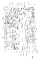
- FIG. 2 is a perspective view of the printed wiring board 70 on which the components are mounted.
- various components constituting the inverter circuit 40, the active filter circuit 60, the switching power supply 80, and the like shown in FIG. 1 are mounted on the printed wiring board 70. This eliminates the need for a harness for connecting each circuit, and makes it possible to reduce the size and cost of the power conversion device 10.
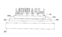
- Heat sink 200 As shown in FIG. 2, a heat sink 200 is installed in the inverter module 30 in order to promote heat dissipation from the switching circuit 25 that becomes hot.
- FIG. 3 is a plan view of the heat sink 200 shown in FIG. 2 in a state of being inverted 180 ° to the right with respect to the right end of the front view.
- the heat sink 200 is equipped with not only the inverter module 30, but also the active filter module 50 and the fan power module 120.
- the heat sink 200 is also used as a cooler for cooling the active filter module 50 and the fan power module 120.
- the power conversion device 10 can be made smaller, lighter, and less costly.
- the heat sink 200 has a cooling unit 201 and an endothermic unit 203.
- a heat transfer tube through which the refrigerant flows is attached to the cooling unit 201.
- the heat transfer tube is unnecessary.
- the heat sink 200 is grounded from the heat absorbing portion 203 via the ground wire 190.
- the endothermic unit 203 transfers the heat from the inverter module 30, the active filter module 50, and the fan power module 120 to the cooling unit 201.
- the endothermic unit 203 includes a heat absorbing surface 203a surrounded by a long side parallel to the longitudinal direction of the cooling unit 201 and a short side orthogonal to the longitudinal direction thereof.
- An inverter module 30, an active filter module 50, and a fan power module 120 are mounted on the heat absorbing surface 203a of the heat absorbing portion 203.
- the inverter module 30, the active filter module 50, and the fan power module 120 are all rectangular parallelepipeds.
- the length of the short side of the active filter module 50 is equal to or greater than the short side of the endothermic surface 203a and less than or equal to the short side of the inverter module 30.
- the package of the active filter module 50 is smaller than that of the inverter module 30, when the active filter module 50 is attached to the heat absorbing portion 203, the distance between the terminal of the active filter module 50 and the heat absorbing portion 203 becomes short, and the inverter module in creepage distance and space distance. It is more disadvantageous than 30. Therefore, the disadvantage is overcome by interposing a first heat transfer member 220 that raises the impedance between the active filter module 50 and the heat sink 200.
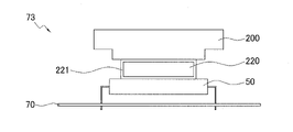
- FIG. 4 is a perspective view of the heat sink 200 and the active filter module 50 shown in FIG. 3 as viewed from the front side.
- a first heat transfer member 220 is arranged between the heat sink 200 and the active filter module 50.
- the first heat transfer member 220 is made of aluminum or an aluminum alloy. The function of the first heat transfer member 220 is to adjust the height with the inverter module 30 and to transfer the heat of the active filter module 50 to the heat sink 200.
- the heat sink 200 is an inverter module 30, an active filter module 50, and a fan power module mounted on one printed wiring board 70. It is also used as a heat sink for cooling the 120.
- the inverter module 30, the active filter module 50, and the fan power module 120 have different heights from the mounting surface of the printed wiring board 70, and among the three modules, the inverter module 30 is from the mounting surface of the printed wiring board 70. The height is the highest.
- a member for height adjustment is sandwiched between the heat dissipation surface of the active filter module 50 and the fan power module 120 and the heat sink 200 so that the heat sink 200 is parallel to the mounting surface of the printed wiring board 70. It is configured in.
- the height adjusting member arranged between the heat radiating surface of the active filter module 50 and the heat sink 200 is the first heat transfer member 220.
- the thickness of the first heat transfer member 220 is not simply determined by the facing distance between the heat dissipation surface of the active filter module 50 and the heat sink 200.
- the thickness of the first heat transfer member 220 is determined after determining suitability based on the physical quantity of the potential difference between the terminal of the active filter module 50 and the heat sink 200.
- the thickness of the first heat transfer member 220 is not appropriate from the viewpoint of the potential difference, the facing distance itself is readjusted. As a result, the thickness of the first heat transfer member 220 is appropriately set without excess or deficiency.
- the first heat transfer member 220 is interposed between the heat dissipation surface of the active filter module 50 and the heat sink 200, heat is efficiently transferred from the active filter module 50 to the heat sink 200. There must be. Therefore, it is manufactured of a highly heat-conducting material (for example, "aluminum” or “aluminum alloy” or “copper” or “copper alloy” or “ceramic material”).
- first heat transfer member 220 aluminum or an aluminum alloy is used as the first heat transfer member 220.
- FIG. 5 is an equivalent circuit of the common mode.
- the LISN is a noise measuring device, not a component of the circuit of FIG.
- the active filter module 50 cancels out the harmonic components generated by the inverter module 30 by switching.
- the resonance frequency may be removed from the target frequency band of the noise terminal voltage by increasing the reactance value of the connected reactor 54, or the carrier filter 53 may be strengthened, but the size of the printed wiring board 70 may be increased. , Invites an increase in the size of electrical components.
- the parasitic capacitance between the active filter module 50 and the heat sink 200 is reduced, and the common mode noise is suppressed. ..
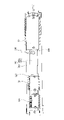
- FIG. 6A is a side view of the first printed wiring board assembly 71.
- the first heat transfer member 220 is interposed between the active filter module 50 and the heat sink 200.
- FIG. 6B is a side view of the second printed wiring board assembly 72.
- the first heat transfer member 220 and the insulating sheet 230 are interposed between the active filter module 50 and the heat sink 200.
- FIG. 6C is a side view of the third printed wiring board assembly 73.
- the first heat transfer member 220 subjected to alumite treatment is interposed between the active filter module 50 and the heat sink 200.
- Alumite treatment is a surface treatment that electrolyzes the surface of aluminum with an anode to form an oxide film. Therefore, the surface of the first heat transfer member 220 is covered with the oxide film 221.
- FIG. 7 is a graph comparing the parasitic capacitance between the active filter module 50 and the heat sink 200 in the first printed wiring board assembly 71, the second printed wiring board assembly 72, and the third printed wiring board assembly 73.
- the parasitic capacitance is largest in 62 of the first printed wiring board assembly 71, followed by 50 of the third printed wiring board assembly 73 and 21 of the second printed wiring board assembly 72 in this order.
- the active filter module 50 EMI gets worse when it works.
- the noise component passes through the carrier filter 53 because the ground impedance of the heat sink 200 is large, so that the noise component is reduced and the active filter module 50 is used. Deterioration of EMI during operation is improved.
- the first heat transfer member 220 subjected to the alumite treatment of FIG. 6C is interposed between the active filter module 50 and the heat sink 200 to suppress common mode noise. ing.
- the printed wiring board 70 is a multilayer printed wiring board having a plurality of conductive pattern layers laminated with an insulator layer interposed therebetween.
- the first layer, the second layer, and the third layer are arranged from top to bottom with the surface on which various electric components constituting the inverter circuit 40, the active filter circuit 60, and the switching power supply 80 are mounted facing up.
- the fourth conductive pattern layer is laminated.
- 8A, 8B, 8C and 8D show a part of the conductive pattern of each of the first layer Z1, the second layer Z2, the third layer Z3 and the fourth layer Z4 of the printed wiring board 70. It is a top view of the plate 70.
- each layer is divided into 16 regions in a plan view, and each region is designated by a reference numeral indicating its position.
- the position of the lower left region is set to X1, and the number behind X increases by one each time the region is moved in the X direction. Further, each time the area is moved from Y1 to the Y direction, the number after Y is incremented by one.
- the number after Z increases by one. Specifically, the region at the upper right end of the fourth layer Z4 in FIG. 8D in a plan view is displayed as the region X4Y4Z4.
- the regions having the same number after X and the number after Y are configured so as to completely overlap when viewed from the stacking direction.
- FIG. 9 shows the positional relationship of each pattern when the first layer Z1, the second layer Z2, the third layer Z3, and the fourth layer Z4 are laminated and viewed from the first layer Z1 side toward the stacking direction. It is a top view of the printed wiring board 70.
- the low voltage pattern for current detection is formed so as not to overlap with the high voltage pattern formed in the other layers when viewed from the stacking direction.
- the 1st 1-A low voltage pattern 41L is formed in the region X4Y3Z1 in the first layer Z1.
- the 1st 1-A low voltage pattern 41L is a conductive pattern used for current detection of the inverter module 30. The current detection of the inverter module 30 is performed via the current detection unit 33.
- the high voltage pattern is generated. not exist.
- the current of the inverter circuit 40 can be detected with high accuracy.
- the first 1-B low voltage pattern 61L is formed in the region X2Y3Z1.
- the first 1-B low voltage pattern 61L is a conductive pattern used for current detection of the active filter module 50. The current detection of the active filter module 50 is performed via the current detection unit 57.
- the high voltage pattern is generated. not exist.
- the inverter circuit 40 Even if the inverter circuit 40 operates, noise does not overlap with the 1-B low voltage pattern 61L. Therefore, the current of the active filter module 50 can be detected with high accuracy.
- First high voltage pattern 61H Further, in the first layer Z1, the first high voltage pattern 61H is formed in the regions X2Y4Z1, X3Y4Z1, X2Y3Z1, X3Y3Z1 and X3Y2Z1.
- the first high voltage pattern 61H is a high voltage line connecting the output side of the rectifier circuit 20 and the input side of the active filter circuit 60.
- Second layer Z2 In the second layer, the low voltage patterns other than those for current detection and those for voltage detection are formed so as to overlap with the high voltage patterns formed in the other layers when viewed from the stacking direction.
- Second low voltage pattern 42L In FIG. 8B, a second low voltage pattern 42L is formed in the region X2Y1Z2 in the second layer Z2.
- the second low voltage pattern 42L is a low voltage line used for transmitting on / off signals of each relay for controlling the refrigerant.
- the third A high voltage pattern 43H (for example, an air conditioner) that is not the inverter circuit 40 and the active filter circuit 60 (for example, an air conditioner).
- a high voltage pattern such as a switching power supply circuit, an outdoor fan circuit, a refrigerant control circuit, and a connection circuit to an indoor unit.
- the second low voltage pattern 42L And the third-A high voltage pattern 43H partially overlap each other in the stacking direction.
- noise is removed by a CR filter before entering the microcomputer and relay for the signal passing through the second low voltage pattern 42L.
- the second low voltage pattern 42L which is not related to the detection of current or voltage, it is allowed that a part of the second low voltage pattern 42L overlaps with the third 3-A high voltage pattern 43H in the stacking direction. By doing so, the degree of freedom in designing the printed wiring board 70 is increased.
- Second high voltage pattern 52H Further, in the second layer Z2, the second high voltage pattern 52H is formed in the regions X4Y2Z2 and X4Y1Z2. A high voltage supplied to the inverter circuit 40 and the active filter circuit 60 is supplied to the second high voltage pattern 52H.
- Third layer Z3 In the third layer, a part of the low voltage pattern other than the current detection and the voltage detection is formed so as to overlap with the high voltage pattern formed in the other layers when viewed from the stacking direction.
- Third 3-A low voltage pattern 83L1 In FIG. 8C, the third layer Z3 has a third 3-A low voltage pattern 83L formed in the regions X1Y2Z3, X2Y2Z3, X3Y2Z3 and X4Y2Z3.
- the third 3-A low voltage pattern 83L is a supply line for each output voltage (5V, 15V, etc.) generated by the switching power supply 80.
- the second high voltage pattern 52H exists in the region X4Y2Z2 of the second layer Z2 that overlaps with the region X4Y2Z3 in which a part of the third 3-A low voltage pattern 83L1 exists in the stacking direction, as shown in the R2 portion of FIG.
- the third 3-A low voltage pattern 83L1 and the second high voltage pattern 52H partially overlap each other in the stacking direction.
- the signal passing through the 3-A low voltage pattern 83L1 is noise-reduced by a CR filter before entering the microcomputer and the power module.
- the third-A low voltage pattern 83L1 which is not related to the detection of current or voltage, a part of the third-A low voltage pattern 83L1 overlaps with the second high voltage pattern 52H in the stacking direction.
- the third layer Z3 has a third-B low voltage pattern 83L2 formed in the region X4Y1Z3.
- the third 3-B low voltage pattern 83L2 is a low voltage line used for transmitting the on / off signal of the main relay 93.
- the second high voltage pattern 52H exists in the region X4Y1Z2 of the second layer Z2 that overlaps with the region X4Y1Z3 in which the third 3-B low voltage pattern 83L2 exists in the stacking direction, and as shown in the R3 portion of FIG.
- the 3-B low voltage pattern 83L2 and the second high voltage pattern 52H partially overlap each other in the stacking direction.
- the signal passing through the 3-B low voltage pattern 83L2 is noise-reduced by a CR filter before entering the microcomputer and the relay.
- the third-B low voltage pattern 83L2 which is not related to the detection of current or voltage, a part of the third-B low voltage pattern 83L2 overlaps with the second high voltage pattern 52H in the stacking direction.
- the third 3-A high voltage pattern 43H is a high voltage line that is not the inverter circuit 40 and the active filter circuit 60 (for example, in the case of an air conditioner, a connection to a switching power supply circuit, an outdoor fan circuit, a refrigerant control circuit, and an indoor unit. It is a high voltage pattern for circuits, etc.).
- Fourth layer Z4 In the fourth layer Z4, the low voltage patterns for voltage detection and current detection are formed so as not to overlap with the high voltage patterns formed in the other layers when viewed from the stacking direction.
- the 4-A low voltage pattern 44L is formed in the regions X3Y4Z4, X4Y4Z4, X4Y3Z4 and X4Y2Z4.
- the 4-A low voltage pattern 44L is a conductive pattern used for voltage detection of the inverter module 30. The voltage detection of the inverter module 30 is performed via the voltage detection unit 32.
- the region X4Y3Z1 of the first layer, the region X4Y3Z2 of the second layer Z2, and the region X4Y3Z3 of the third layer Z3, which overlap with the region X4Y3Z4 in which a part of the fourth 4-A low voltage pattern 44L exists in the stacking direction, have a second layer. There is no high voltage pattern that overlaps a part of the 4-A low voltage pattern 44L in the stacking direction. Therefore, for example, even if the active filter circuit 60 operates, noise is not superimposed on the 4-A low voltage pattern 44L. Therefore, the voltage of the inverter circuit 40 can be detected with high accuracy.
- the 4-B low voltage pattern 64L1 is formed in the region X3Y3Z4.
- the 4-B low voltage pattern 64L1 is a conductive pattern used for voltage detection of the active filter circuit 60. The voltage detection of the active filter circuit 60 is performed via the voltage detection unit 56.
- a part of the first high voltage pattern 61H exists in the region X3Y3Z1 of the first layer Z1 which overlaps with the region X3Y3Z4 in which the fourth 4-B low voltage pattern 64L1 exists in the stacking direction. Therefore, the 4-B low voltage pattern 64L1 overlaps with a part of the first high voltage pattern 61H in the stacking direction.
- the first high voltage pattern 61H is a high voltage line connecting the output side of the rectifying circuit 20 and the input side of the active filter circuit 60, and the first high voltage pattern 61H and the 4-B low voltage pattern 64L1 are Both belong to the active filter circuit 60.
- the low voltage pattern for voltage or current detection and the high voltage pattern may overlap in the stacking direction.
- the voltage or current detection low voltage pattern belonging to the inverter circuit 40 overlaps with the high voltage pattern belonging to the inverter circuit 40 in the stacking direction. Even in such a case, it is not affected by the noise that occurs when it overlaps with other high voltage patterns that do not belong to the inverter circuit 40 in the stacking direction.
- the 4-C low voltage pattern 64L2 is formed in the regions X3Y3Z4, X2Y2Z4 and X3Y2Z4.
- the fourth 4-C low voltage pattern 64L2 is a conductive pattern used for current detection of the active filter circuit 60. The current detection of the active filter circuit 60 is performed via the U-phase current detection unit 58u and the W-phase current detection unit 58w.
- a part of the first high voltage pattern 61H exists in the region X3Y2Z1 of the first layer Z1 which overlaps with the region X3Y2Z4 in which a part of the fourth 4-C low voltage pattern 64L2 exists in the stacking direction. Therefore, the 4-C low voltage pattern 64L2 overlaps with a part of the first high voltage pattern 61H in the stacking direction.
- the first high voltage pattern 61H is a high voltage line connecting the output side of the rectifying circuit 20 and the input side of the active filter circuit 60, and the first high voltage pattern 61H and the 4-C low voltage pattern 64L2 are Both belong to the active filter circuit 60.
- the printed wiring board 70 has three areas along the Y direction, with the long side direction of the printed wiring board 70 being the X direction and the short side direction being the Y direction. It is a perspective view of the printed wiring board 70 when it is virtually divided into 1 area 701, the 2nd area 702 and the 3rd area 703.
- the first area 701 is a range from the first end 70Y, which is one end of the printed wiring board 70 in the Y direction, to a distance of about 1/3 of the length of the printed wiring board 70 in the Y direction.
- the third area 703 is a range from the second end 70Yb, which is the other end of the printed wiring board 70 in the Y direction, to a distance of 1/3 of the length of the printed wiring board 70 in the Y direction.
- a carrier filter 53 which can be said to be a heavy object, and a connected reactor 54 are arranged among the parts constituting the active filter circuit 60.
- these heavy objects are referred to as "first heavy objects 601".
- the transformer 81 which can be said to be a heavy object among the parts constituting the switching power supply 80, is also arranged in the first area 701.
- the heavy object 601 of the active filter circuit 60 is the first.
- One area 701 is arranged on one end side in the X direction, and the transformer 81 of the switching power supply 80 is arranged on the other end side in the X direction of the first area 701.
- Second area 702 In the second area 702 sandwiched between the first area 701 and the third area 703, the inverter module 30, the active filter module 50, and the fan power module 120 are placed in the long side direction of the printed wiring board 70 (X in FIG. 10). It is arranged along the direction).
- a common heat sink 200 is attached to the inverter module 30, the active filter module 50, and the fan power module 120. Therefore, the heat sink 200 has a shape extending along the X direction in FIG.
- Third area 703 In the third area 703, a reactor 24, which can be said to be a heavy object, is arranged among the parts constituting the inverter circuit 40.
- the heavy object is referred to as "second heavy object 401".
- FIG. 11A shows the printed wiring board 70 conveyed on the solder tank 730 and the first heavy object 601 having the center of gravity in the second area 702 of the printed wiring board 70. It is a front view which looked at the 2nd heavy object 401 from the transport direction.
- FIG. 11B shows a printed wiring board 70 carried on the solder tank 730, a first heavy object 601 having a center of gravity in the first area 701 of the printed wiring board 70, and a second center of gravity placed in the third area 703. It is a front view which looked at the heavy object 401 from the transport direction.
- the solder tank 730 is filled with the molten solder 720.
- Conveyors 710 for moving the printed wiring board 70 are installed at both ends of the opening of the solder tank 730.
- the conveyor 710 sandwiches the first end 70Ya and the second end 70Yb of the printed wiring board 70, and conveys the printed wiring board 70 on the liquid surface of the molten solder 720 at a predetermined speed.
- the transport direction is the long side direction of the printed wiring board 70 (X direction in FIG. 10).
- the liquid level of the molten solder 720 is rippling due to the jet flow, and the soldering surface of the printed wiring board 70 is filled with solder with that momentum.
- the printed wiring board 70 can move smoothly on the solder tank 730, and it is possible to suppress a state in which it becomes difficult for solder to adhere.
- a printed wiring board assembly (see FIG. 10) in which electrical components are soldered to the printed wiring board 70 is completed.
- the operator transports the printed wiring board assembly to the next process, if the printed wiring board assembly is transported with the first area 701 and the third area 703, the printed wiring board 70 will not be unnecessarily distorted.
- the inverter module 30, the active filter module 50, and the fan power module 120 having a plurality of electrode pins are arranged side by side in the long side direction (X direction in FIG. 10), and their electrodes are arranged. Since the pins are soldered to the printed wiring board 70, the inverter module 30, the active filter module 50, and the fan power module 120 are reinforcing members of the second area 702.
- the inverter module 30, the active filter module 50 and the fan power module 120 are screwed to one heat sink 200 extending in the long side direction (X direction in FIG. 10) of the second area 702, the second area 702 is connected. Two areas 702 are indirectly reinforced.
- the second area 702 includes the inverter module 30, the active filter module 50, the fan power module 120, and the heat sink 200. Since it is reinforced by, it can withstand distortion and bending.
- Control voltage of the active filter module 50 As shown in FIG. 1, in the active filter circuit 60, the input of the AC power supply 100 is connected to the connection points NU, NV, and NW of the active filter module 50, and the active filter module The first capacitor 52 is connected between the P and N terminals of the 50.
- the active filter module 50 itself receives the inrush current when the voltage of the power supply drops or recovers from a power failure, or the inrush current due to the fluctuation of the power supply frequency during operation, and the active filter module 50 is required to withstand the inrush current. Will be done.
- the active filter circuit was mounted on the board dedicated to the active filter circuit as an option. Therefore, in order to support a plurality of horsepower models with one type of active filter dedicated board, the active filter module is equipped with a large rated current suitable for the model with the highest horsepower. Therefore, the inrush current withstand of the active filter module itself is high, and it is not necessary to worry about the inrush current withstand of the active filter module.
- the active filter module 50 with the optimum rated current according to the horsepower of the applicable model. Need to be set.
- the inrush current withstand of the active filter module 50 itself becomes lower than that of the conventional product, and there is a risk that the active filter module 50 will fail due to the inrush current.
- the ambient temperature of the printed wiring board 70 was set to -35 ° C, 25 ° C, or 70 ° C, and at each ambient temperature, the power supply voltage was 85% of the rated voltage, 100% of the rated voltage, or the rated voltage.
- the content is to set the voltage to 115% of the above, switch the power supply frequency from 50Hz to 60Hz or 60Hz to 50Hz at each power supply voltage, and check the inrush current withstand.
- control voltage of the active filter module 50 was set to 15.0V, 15.5V, 16.0V and 16.5V for confirmation.
- FIG. 12 is a table showing the results of the inrush current proof stress experiment of the active filter module 50.
- 15 V which is a general control voltage of the active filter module 50
- the compensation current of the active filter module 50 is large under any condition. An inrush current was generated and the operation of the active filter module 50 was stopped, or the active filter module 50 itself was damaged.
- control voltage of the active filter module 50 is that when the control voltage is set to the general 15V, the current withstand is about 220% of the rated current, and when the control voltage is set to 16V or more, the current withstand is It becomes 250% or more of the rated current. If the control voltage of the active filter module 50 is increased, the current bearing capacity tends to increase.
- the control voltage of the active filter module 50 is set to 16.5 V in consideration of a margin.
- the control voltage of the active filter module 50 is set to 16.5 V, which is higher than the general 15 V.
- the inrush current withstand of the active filter module 50 itself is increased, and the active filter module 50 is prevented from being damaged due to the inrush current when the voltage of the power supply drops or recovers from a power failure, or the power frequency fluctuation during operation. ing.
- the demerit of increasing the control voltage of the active filter module 50 is that the short-circuit tolerance time of the active filter module 50 is shortened.
- the upper limit of the control voltage of the active filter module 50 is 22V, but it is preferable to keep it at 18V in consideration of the short circuit resistance time.
- the damage is limited to the active filter circuit 60. Therefore, the damage is smaller than the case where the inverter circuit 40 is damaged and the motor M needs to be replaced.
- the control voltage of the active filter module 50 may be increased to 20 V at the expense of shortening the short-circuit tolerance time.
- control voltage of the active filter module 50 is preferably 16V to 20V.
- Control voltage of the inverter module 30 For example, when the motor M is a motor of a variable capacity compressor, as shown in FIG. 1, the corresponding phases are from the connection points NU, NV, and NW of the inverter module 30.
- the output line extends toward the drive coils Lu, Lv, and Lw.
- the inverter module 30 is short-circuited, not only the inverter circuit 40 but also the compressor will be damaged. Therefore, even if the inverter module 30 is short-circuited, the short-circuit endurance of the inverter module 30 is necessary to prevent the compressor from being damaged.
- control voltage of the inverter module 30 is set to 14.5V so that the short circuit endurance time is longer than that of the active filter module 50.
- the inverter module since the inverter circuit 40 is connected to the downstream side of the rectifier circuit 20 when viewed from the AC power supply side, the inverter module measures the input current at the time of recovery from the power supply voltage drop / power failure and the inrush current due to the power supply frequency fluctuation during operation. 30 does not receive it directly. Therefore, the inverter module 30 is not required to have the inrush current bearing capacity of the active filter module 50. Therefore, the lower limit of the control voltage of the inverter module 30 may be 13V.
- the active filter circuit 60 and the inverter circuit 40 are mounted on one printed wiring board 70, so that the power conversion device 10 can be made smaller, lighter, and less costly.
- the printed wiring board 70 is a multilayer printed wiring board having a plurality of conductive pattern layers laminated with an insulator layer interposed therebetween. Since the low voltage pattern for detecting the current or voltage of the active filter circuit 60 and the high voltage pattern of the inverter circuit 40 do not overlap in the stacking direction, even if the inverter circuit 40 operates, the active filter circuit 60 is concerned. No noise is superimposed on the low voltage pattern. Therefore, the current or voltage of the active filter circuit 60 is accurately detected.
- one switching power supply circuit 80 that supplies power to the active filter circuit 60 and the inverter circuit 40 is mounted on the printed wiring board 70. Since it is not necessary for each of the active filter circuit 60 and the inverter circuit 40 to have a switching power supply circuit individually, the power conversion device 10 can be made smaller, lighter, and less costly.
- the mounting areas of the switching power supply circuit 80, the active filter circuit 60, and the inverter circuit 40 on the mounting surface of the printed wiring board 70 are separated. Further, the circuit areas of the switching power supply circuit 80, the active filter circuit 60, and the inverter circuit 40 in the printed wiring board 70 are also divided in the stacking direction of the printed wiring board 70. As a result, the low voltage pattern for detecting the current or voltage does not overlap with the high voltage pattern belonging to a circuit different from the circuit to which the low voltage pattern belongs in the stacking direction.
- the current limiting circuit 90 that limits the current flowing through the smoothing capacitor 22 is also used as the current limiting circuit that limits the current flowing through the first capacitor 52 of the active filter circuit 60. Therefore, it is not necessary for the active filter circuit 60 to individually have a current limiting circuit, and the power conversion device 10 can be made smaller, lighter, and less costly.
- the heat sink 200 for cooling the inverter module 30 of the inverter circuit 40 is also used as a heat sink for cooling the active filter module 50. Therefore, since the inverter module 30 and the active filter module 50 can be cooled by one heat sink 200, the power conversion device 10 can be made smaller, lighter, and lower in cost.
- the first heavy object 601 becomes the first area 701.
- the second heavy object 401 is arranged in the third area 703.
- the heavy electrical components, the first heavy object 601 and the second heavy object 401, are prevented from being biased to one area, and the weight of the first heavy object 601 and the second heavy object 401 causes distortion and bending of the printed wiring board 70. It is less likely to occur.
- the second area 702 is reinforced by mounting the inverter module 30, the active filter module 50, and the fan power module 120 in the second area 702. As a result, there is no need to add a new reinforcing member.
- the second area 702 is further reinforced by fastening one heat sink 200 common to the inverter module 30, the active filter module 50, and the fan power module 120 with screws.
- the printed wiring board 70 is conveyed on the solder tank 730 in parallel with the long side direction of the printed wiring board 70, and is used for the inverter module 30, the active filter module 50, and the fan along the long side direction.
- the power modules 120 are arranged, and the heat sink 200 extends along the arrangement direction. Therefore, the strength of the second area 702 in the long side direction is increased, which increases the strength of the printed wiring board 70 itself in the long side direction.
- the first heavy object 601 includes a reactor 54 connected to the reactor of the carrier filter 53, and the second heavy object 401 includes a reactor 24. Since these reactors are heavier than the inverter module 30, the active filter module 50, and the fan power module 120, the first area 701 having the first end 70Ya of the printed wiring board 70 and the third area having the second end 70Yb It is implemented in 703.
- the operator naturally grasps both ends of the printed wiring board 70. As a result, the printed wiring board 70 is suppressed from being distorted and bent because it has the first heavy object 601 side and the second heavy object 401 side.
- each component of the first heavy object 601 is arranged along the long side direction of the first area 701 having the first end 70Ya of the printed wiring board 70, and the third area 703 having the second end 70Yb is arranged.
- Each part of the second heavy object 401 is lined up along the long side direction.
- the printed wiring board 70 has the first heavy object 601 mounted on the first area 701 having the first end 70Ya, and the second heavy object 401 in the third area 703 having the second end 70Yb. Is placed, it passes through the solder tank 730 along the long side direction of the printed wiring board 70.
- the conveyor 710 of the solder tank 730 holds the first end 70Ya and the second end 70Yb of the printed wiring board 70 and conveys the printed wiring board 70. Since there is no heavy object in the second area 702, which is the central portion of the printed wiring board 70, the printed wiring board 70 does not bend in a concave shape, and soldering defects due to distortion and bending are suppressed.
- the first heat transfer member 220 is arranged between the active filter module 50 and the heat sink 200.
- the impedance between the active filter module 50 and the heat sink 200 increases, and the parasitic capacitance between the active filter module 50 and the heat sink 200 decreases.
- the ground impedance of the heat sink 200 becomes large, the noise component passes through the existing carrier filter 53, the noise component is reduced, and the deterioration of the EMI (noise terminal voltage) during the operation of the active filter circuit 60 is suppressed. Will be done.
- the active filter circuit 60 and the inverter circuit 40 are mounted on the same printed wiring board, and by making one board, parts can be saved and costs can be reduced.
- the thickness of the first heat transfer member 220 is determined by the physical quantity of the potential difference between the terminal of the active filter module 50 and the heat sink 200, so that the thickness of the first heat transfer member 220 is not excessive or insufficient. Set properly.
- the ground impedance can be adjusted by surface treatment of the first heat transfer member 220, the ground impedance is maintained without the need for other members and the heat transfer property of the first heat transfer member 220 is maintained. Can be adjusted.
- the active filter circuit 60 by setting the control voltage of the active filter module 50 to 16.0 V or higher, which is higher than the general 15 V, the inrush current withstand strength of the switching element can be increased and the breaking strength of the switching element can be increased. can.
- control voltage of the active filter module 50 is set to 16.5V.
- the inrush current withstand is smaller than the inrush current withstand required for the active filter module 50. Therefore, the control voltage of the inverter module 30 can be made smaller than the control voltage of the active filter module 50.
- control voltage of the inverter module 30 is 15.5V or less, and the lower limit is 13V.
- a second heat transfer member 250 may be interposed between the inverter module 30 and the heat sink 200.
- the effect of increasing the impedance between the inverter module 30 and the heat sink 200 by the second heat transfer member 250 is larger than the effect of increasing the impedance between the active filter module 50 and the heat sink 200 by the first heat transfer member 220. It may be small.
- heat transfer grease is adopted as the second heat transfer member 250.
Landscapes
- Engineering & Computer Science (AREA)
- Power Engineering (AREA)
- Inverter Devices (AREA)
- Amplifiers (AREA)
- Polarising Elements (AREA)
Abstract
Description
図1は、本開示の一実施形態に係る電力変換装置10の構成を示す回路図である。図1において、電力変換装置10は、整流回路20と、インバータ回路40と、アクティブフィルタ回路60と、スイッチング電源80と、1つのプリント配線板70とを備えている。 (1) Outline of
(2-1)整流回路20
整流部21は、6つのダイオードD0a,D0b,D1a,D1b,D2a,D2bによってブリッジ状に構成されている。具体的には、ダイオードD0aとD0b、D1aとD1b、D2aとD2bは、それぞれ互いに直列に接続されている。 (2) Detailed configuration (2-1)
The rectifying unit 21 is configured in a bridge shape by six diodes D0a, D0b, D1a, D1b, D2a, and D2b. Specifically, the diodes D0a and D0b, D1a and D1b, and D2a and D2b are connected in series with each other.
インバータ回路40は、リアクトル24と、平滑コンデンサ22と、インバータモジュール30、電圧検出部32と、電流検出部33と、インバータマイコン35とを有している。 (2-2)
The
リアクトル24は、その一端が整流回路20の正側出力端子に接続され、その他端が平滑コンデンサ22の正側入力端子に接続されている。 (2-2-1)
One end of the
平滑コンデンサ22は、一端が整流回路20の正側出力端子に接続され、他端が整流回路20の負側出力端子に接続されている。平滑コンデンサ22は、整流回路20によって整流された電圧を平滑する。 (2-2-2) Smoothing
One end of the smoothing
インバータモジュール30は、スイッチング回路25および制御回路26が内蔵され、1つのパッケージになっている。 (2-2-3)
The
スイッチング回路25は、モータMのU相、V相およびW相の駆動コイルLu,Lv,Lwそれぞれに対応する3つの上下アームが互いに並列に、且つ平滑コンデンサ22の出力側に接続されている。 (2-2-3-1)
In the switching
制御回路26は、インバータマイコン35からの指令電圧に基づき、スイッチング回路25の各トランジスタQ3a~Q5bのオンおよびオフの状態を変化させる。 (2-2-3-2)
The
電圧検出部32は、平滑コンデンサ22の出力側に接続されており、平滑コンデンサ22の両端電圧を検出する。電圧検出部32は、例えば、互いに直列に接続された2つの抵抗が平滑コンデンサ22に並列接続され、平滑コンデンサ22の両端電圧が分圧されるように構成される。それら2つの抵抗同士の接続点の電圧値は、インバータマイコン35に入力される。 (2-2-4)
The
電流検出部33は、平滑コンデンサ22およびスイッチング回路25の間であって、かつ平滑コンデンサ22の負側出力端子側に接続されている。電流検出部33は、モータMの起動後、モータMに流れるモータ電流を三相分の電流の合計値として検出する。 (2-2-5)
The
インバータマイコン35は、電圧検出部32、電流検出部33、および制御回路26と接続されている。本実施形態では、インバータマイコン35は、モータMをロータ位置センサレス方式にて駆動させている。なお、ロータ位置センサレス方式に限定されるものではなく、センサ方式で行なってもよい。 (2-2-6)
The
アクティブフィルタ回路60は、アクティブフィルタモジュール50と、第1コンデンサ52と、キャリアフィルタ53と、連繋リアクトル54と、アクティブフィルタマイコン55と、電圧検出部56と、電流検出部57と、U相電流検出部58uと、W相電流検出部58wとを有している。 (2-3)
The
アクティブフィルタモジュール50は、スイッチング回路45および制御回路46が内蔵され、1つのパッケージになっている。 (2-3-1)
The
スイッチング回路45は、高調波電流を抑制するための補償電流を生成する複数のスイッチング素子から成る。 (2-3-1-1)
The switching
制御回路46は、スイッチング素子を制御する。制御回路46の構成も、インバータモジュール30の制御回路26の構成と同じであるので、インバータモジュール30の制御回路26と同じ符号を付して、説明を省略する。 (2-3-1-2)
The
第1コンデンサ52は、スイッチング回路45の出力電力を平滑するコンデンサである。 (2-3-2)
The
キャリアフィルタ53は、スイッチング回路45のスイッチングに伴うノイズを除去する。具体的には、キャリアフィルタ53は、スイッチング回路45のスイッチングによって生じる補償電流の高域成分を除去する。 (2-3-3)
The
連繋リアクトル54は、スイッチング回路45と電源ラインとを連系する。 (2-3-4) Linked
The
アクティブフィルタマイコン55は、電圧検出部56、電流検出部57、U相電流検出部58u、W相電流検出部58w、および制御回路46と接続されている。 (2-3-5)
The
電圧検出部56は、第1コンデンサ52の出力側に接続されており、第1コンデンサ52の両端電圧を検出する。電圧検出部56は、例えば、互いに直列に接続された2つの抵抗が第1コンデンサ52に並列接続され、第1コンデンサ52の両端電圧が分圧されるように構成される。それら2つの抵抗同士の接続点の電圧値は、アクティブフィルタマイコン55に入力される。 (2-3-6)
The
電流検出部57は、第1コンデンサ52およびスイッチング回路45の間であって、かつ第1コンデンサ52の負側出力端子側に接続されている。電流検出部57は、スイッチング回路45の母線電流を検出する。 (2-3-7)
The
U相電流検出部58uは、U相に流れる補償電流を検出する。W相電流検出部58wは、W相に流れる補償電流を検出する。 (2-3-8) U-phase
The U-phase
スイッチング電源80は、整流回路20の出力側に接続されており、インバータマイコン35およびインバータモジュール30の制御回路26に電力を供給する。また、スイッチング電源80は、アクティブフィルタマイコン55およびアクティブフィルタモジュール50の制御回路46にも電力を供給する。 (2-4)
The switching
限流回路90は、限流抵抗91、限流リレー92およびメインリレー93を有している。限流回路90は、平滑コンデンサ22に流れる電流を制限するだけでなく、アクティブフィルタ回路60の第1コンデンサ52に流れる電流を制限する限流回路として兼用される。それゆえ、アクティブフィルタ回路60が個別に限流回路を有する必要がないので、電力変換装置10の小型化、軽量化、低コスト化が図られる。 (2-5) Current limiting circuit 90
The current limiting circuit 90 has a current limiting
限流抵抗91は、交流電源100と整流回路20とを結ぶ三相の電源ラインのうちの1つの電源ライン上に接続されている。 (2-5-1)
The current limiting
限流リレー92は、限流抵抗91が接続されている電源ライン上に、限流抵抗91と直列に接続されている。 (2-5-2) Current limiting
The current limiting
メインリレー93は、交流電源100と整流回路20とを結ぶ三相の電源ラインのうち、限流抵抗91および限流リレー92が接続されている電源ライン上であって、限流抵抗91および限流リレー92と並列に接続されている。さらに、メインリレー93は、限流抵抗91および限流リレー92が接続されていない電源ライン上にも接続されている。 (2-5-3)
The
図2は、部品が実装されているプリント配線板70の斜視図である。図2において、プリント配線板70上には、図1に示すインバータ回路40、アクティブフィルタ回路60およびスイッチング電源80などを構成する各種部品が実装されている。これにより、各回路間を接続するハーネスが不要となり、電力変換装置10の小型化やコストダウンが図られる。 (2-6) Printed
FIG. 2 is a perspective view of the printed
図2に示すように、インバータモジュール30には、高温になるスイッチング回路25からの放熱を促すためにヒートシンク200が設置されている。 (2-7)
As shown in FIG. 2, a
図4は、図3に記載されたヒートシンク200およびアクティブフィルタモジュール50を正面側から視た斜視図である。図4において、ヒートシンク200とアクティブフィルタモジュール50との間には第1伝熱部材220が配置されている。 (2-8) First
FIG. 4 is a perspective view of the
図3に示すように、本実施形態では、ヒートシンク200は、1つのプリント配線板70に実装されたインバータモジュール30、アクティブフィルタモジュール50およびファン用パワーモジュール120を冷却するヒートシンクとして兼用されている。 (2-8-1) Height Adjustment Function As shown in FIG. 3, in the present embodiment, the
第1伝熱部材220は、アクティブフィルタモジュール50の放熱面とヒートシンク200との間に介在するので、アクティブフィルタモジュール50から熱をヒートシンク200に効率的に伝えなければならない。それゆえ、伝熱性の高い材料(例えば、「アルミニウム」若しくは「アルミニウム合金」若しくは「銅」若しくは「銅合金」または「セラミクス材」など)で製造されている。 (2-8-2) Heat transfer function Since the first
図5は、コモンモードの等価回路である。図5において、LISNは、ノイズ測定装置であって、図1の回路の構成要素ではない。 (2-8-3) Countermeasures against common mode noise by the first
プリント配線板70は、絶縁体層を挟んで積層される複数の導電パターン層を有する多層プリント配線板である。 (3) Detailed Configuration of Printed
第1層Z1では、電流検出用の低電圧パターンが、他の層に形成されている高電圧パターンと積層方向から視て、重ならないように形成されている。 (3-1) First layer Z1
In the first layer Z1, the low voltage pattern for current detection is formed so as not to overlap with the high voltage pattern formed in the other layers when viewed from the stacking direction.
図8Aにおいて、第1層Z1には、第1-A低電圧パターン41Lが、領域X4Y3Z1に形成されている。第1-A低電圧パターン41Lは、インバータモジュール30の電流検出に使用される導電パターンである。インバータモジュール30の電流検出は、電流検出部33を介して行われる。 (3-1-1) 1st 1-A
In FIG. 8A, the 1st 1-A
また、第1層Z1には、第1-B低電圧パターン61Lが、領域X2Y3Z1に形成されている。第1-B低電圧パターン61Lは、アクティブフィルタモジュール50の電流検出に使用される導電パターンである。アクティブフィルタモジュール50の電流検出は、電流検出部57を介して行われる。 (3-1-2) 1st-B
Further, in the first layer Z1, the first 1-B
さらに、第1層Z1には、第1高電圧パターン61Hが、領域X2Y4Z1、X3Y4Z1、X2Y3Z1、X3Y3Z1およびX3Y2Z1に形成されている。第1高電圧パターン61Hは、整流回路20の出力側とアクティブフィルタ回路60の入力側とを繋ぐ高電圧ラインである。 (3-1-3) First
Further, in the first layer Z1, the first
第2層では、電流検出用および電圧検出用以外の低電圧パターンが、他の層に形成されている高電圧パターンと積層方向から視て、重なるように形成されている。 (3-2) Second layer Z2
In the second layer, the low voltage patterns other than those for current detection and those for voltage detection are formed so as to overlap with the high voltage patterns formed in the other layers when viewed from the stacking direction.
図8Bにおいて、第2層Z2には、第2低電圧パターン42Lが、領域X2Y1Z2に形成されている。第2低電圧パターン42Lは、冷媒制御用の各リレーのオン・オフ信号の伝送に使用される低電圧ラインである。 (3-2-1) Second
In FIG. 8B, a second
また、第2層Z2には、第2高電圧パターン52Hが、領域X4Y2Z2およびX4Y1Z2に形成されている。第2高電圧パターン52Hには、インバータ回路40およびアクティブフィルタ回路60に供給する高電圧が供給される。 (3-2-2) Second
Further, in the second layer Z2, the second
第3層では、電流検出用および電圧検出用以外の低電圧パターンの一部が、他の層に形成されている高電圧パターンと積層方向から視て、重なるように形成されている。 (3-3) Third layer Z3
In the third layer, a part of the low voltage pattern other than the current detection and the voltage detection is formed so as to overlap with the high voltage pattern formed in the other layers when viewed from the stacking direction.
図8Cにおいて、第3層Z3には、第3-A低電圧パターン83Lが、領域X1Y2Z3、X2Y2Z3、X3Y2Z3およびX4Y2Z3に形成されている。第3-A低電圧パターン83Lは、スイッチング電源80で生成された各出力電圧(5V、15Vなど)の供給ラインである。 (3-3-1) Third 3-A low voltage pattern 83L1
In FIG. 8C, the third layer Z3 has a third 3-A low voltage pattern 83L formed in the regions X1Y2Z3, X2Y2Z3, X3Y2Z3 and X4Y2Z3. The third 3-A low voltage pattern 83L is a supply line for each output voltage (5V, 15V, etc.) generated by the switching
図8Cにおいて、第3層Z3には、第3-B低電圧パターン83L2が、領域X4Y1Z3に形成されている。第3-B低電圧パターン83L2は、メインリレー93のオン・オフ信号の伝送に使用される低電圧ラインである。 (3-3-2) Third 3-B low voltage pattern 83L2
In FIG. 8C, the third layer Z3 has a third-B low voltage pattern 83L2 formed in the region X4Y1Z3. The third 3-B low voltage pattern 83L2 is a low voltage line used for transmitting the on / off signal of the
また、第3層Z3には、第3-A高電圧パターン43Hが、領域X2Y1Z3に形成されている。第3-A高電圧パターン43Hは、インバータ回路40およびアクティブフィルタ回路60ではない高電圧ラインである(例えば、空調機の場合、スイッチング電源回路、室外ファン回路、冷媒制御回路、室内機への接続回路などの高電圧パターンである。)。 (3-3-3) Third-A
Further, on the third layer Z3, the third-A
第4層Z4では、電圧検出用および電流検出用の低電圧パターンが、他の層に形成されている高電圧パターンと積層方向から視て、重ならないように形成されている。 (3-4) Fourth layer Z4
In the fourth layer Z4, the low voltage patterns for voltage detection and current detection are formed so as not to overlap with the high voltage patterns formed in the other layers when viewed from the stacking direction.
図8Dにおいて、第4層Z4には、第4-A低電圧パターン44Lが、領域X3Y4Z4、X4Y4Z4、X4Y3Z4およびX4Y2Z4に形成されている。第4-A低電圧パターン44Lは、インバータモジュール30の電圧検出に使用される導電パターンである。インバータモジュール30の電圧検出は、電圧検出部32を介して行われる。 (3-4-1) 4th-A
In FIG. 8D, in the fourth layer Z4, the 4-A
また、第4層Z4には、第4-B低電圧パターン64L1が、領域X3Y3Z4に形成されている。第4-B低電圧パターン64L1は、アクティブフィルタ回路60の電圧検出に使用される導電パターンである。アクティブフィルタ回路60の電圧検出は、電圧検出部56を介して行われる。 (3-4-2) 4th-B low voltage pattern 64L1
Further, on the fourth layer Z4, the 4-B low voltage pattern 64L1 is formed in the region X3Y3Z4. The 4-B low voltage pattern 64L1 is a conductive pattern used for voltage detection of the
さらに、第4層Z4には、第4-C低電圧パターン64L2が、領域X3Y3Z4、X2Y2Z4およびX3Y2Z4に形成されている。第4-C低電圧パターン64L2は、アクティブフィルタ回路60の電流検出に使用される導電パターンである。アクティブフィルタ回路60の電流検出は、U相電流検出部58uおよびW相電流検出部58wを介して行われる。 (3-4-3) 4th 4-C low voltage pattern 64L2
Further, on the fourth layer Z4, the 4-C low voltage pattern 64L2 is formed in the regions X3Y3Z4, X2Y2Z4 and X3Y2Z4. The fourth 4-C low voltage pattern 64L2 is a conductive pattern used for current detection of the
図10は、プリント配線板70の長辺方向をX方向、短辺方向をY方向として、プリント配線板70がY方向に沿って3つのエリアである第1エリア701、第2エリア702および第3エリア703に仮想的に区分けされたときの、当該プリント配線板70の斜視図である。 (4) Arrangement of Parts of Printed
第1エリア701には、アクティブフィルタ回路60を構成する部品の中で、重量物といえるキャリアフィルタ53、および連繋リアクトル54が配置されている。説明の便宜上、これらの重量物を「第1重量物601」という。 (4-1)
In the
第1エリア701と第3エリア703とに挟まれた第2エリア702には、インバータモジュール30、アクティブフィルタモジュール50およびファン用パワーモジュール120が、プリント配線板70の長辺方向(図10のX方向)に沿って配置されている。 (4-2)
In the
第3エリア703には、インバータ回路40を構成する部品の中で、重量物といえるリアクトル24が配置されている。説明の便宜上、その重量物を「第2重量物401」という。 (4-3)
In the
図11Aは、ハンダ槽730上を搬送されるプリント配線板70および当該プリント配線板70の第2エリア702に重心を置く第1重量物601と第2重量物401とを搬送方向から視た正面図である。 (4-4) Distortion / Deflection of Printed
図11Aに示すように、プリント配線板70の第2エリア702に第1重量物601の重心および第2重量物401の重心が置かれている場合、プリント配線板70は第2エリア702がハンダ720の液面に近づく方向に撓む。 (4-4-1) Explanation of FIG. 11A As shown in FIG. 11A, when the center of gravity of the first
これに対して、本実施形態では、図11Bに示すように、コンベア710に保持される第1端70Yaを有する第1エリア701に第1重量物601の重心が置かれ、コンベア710に保持される第2端70Ybを有する第3エリア703に第2重量物401の重心が置かれている。それゆえ、プリント配線板70の第2エリア702がハンダ720の液面に近づく方向に撓むことはない。 (4-4-2) Explanation of FIG. 11B On the other hand, in the present embodiment, as shown in FIG. 11B, the first
図1に示すように、アクティブフィルタ回路60では、交流電源100の入力がアクティブフィルタモジュール50の接続点NU、NV、NWに接続されており、アクティブフィルタモジュール50のP、N端子間に第1コンデンサ52が接続されている。 (5) Control voltage of the
例えば、モータMが、容量可変型圧縮機のモータである場合、図1に示すように、インバータモジュール30の接続点NU,NV,NWそれぞれから対応する相の駆動コイルLu,Lv,Lwに向かって出力線が延びている。 (6) Control voltage of the
(7-1)
電力変換装置10では、アクティブフィルタ回路60とインバータ回路40とが1つのプリント配線板70上に実装されることによって、電力変換装置10の小型化、軽量化、低コスト化が図られる。 (7) Features (7-1)
In the
電力変換装置10では、プリント配線板70が、絶縁体層を挟んで積層される複数の導電パターン層を有する多層プリント配線板である。アクティブフィルタ回路60の電流または電圧を検出するための低電圧パターンと、インバータ回路40の高電圧パターンが、積層方向視において重ならないので、インバータ回路40が動作しても、アクティブフィルタ回路60の当該低電圧パターンにノイズが重畳しない。それゆえ、アクティブフィルタ回路60の電流または電圧が精度よく検出される。 (7-2)
In the
電力変換装置10では、アクティブフィルタ回路60の電流または電圧の検出に関係のない低電圧パターンにノイズが重畳しても電流または電圧の検出精度に影響がないので、当該低電圧パターンの一部が積層方向視において高電圧パターンと重なることが許容される。その結果、プリント配線板70の設計自由度が高まる。 (7-3)
In the
インバータ回路40の電流または電圧を検出するための低電圧パターンと、アクティブフィルタ回路60の高電圧パターンが、積層方向視において重ならないので、アクティブフィルタ回路60が動作しても、インバータ回路40の当該低電圧パターンにノイズが重畳しない。それゆえ、インバータ回路40の電流または電圧が精度よく検出される。 (7-4)
Since the low voltage pattern for detecting the current or voltage of the
電力変換装置10では、インバータ回路40の電流または電圧の検出に関係のない低電圧パターンにノイズが重畳しても電流または電圧の検出精度に影響がないので、当該低電圧パターンの一部が積層方向視において高電圧パターンと重なることが許容される。その結果、プリント配線板70の設計自由度が高まる。 (7-5)
In the
電力変換装置10では、アクティブフィルタ回路60およびインバータ回路40に電力供給する1つのスイッチング電源回路80がプリント配線板70に実装されている。アクティブフィルタ回路60およびインバータ回路40それぞれが、個別にスイッチング電源回路を有する必要がないので、電力変換装置10の小型化、軽量化、低コスト化が図られる。 (7-6)
In the
電力変換装置10では、プリント配線板70の実装面におけるスイッチング電源回路80、アクティブフィルタ回路60およびインバータ回路40それぞれの実装エリアが分かれている。さらに、プリント配線板70におけるスイッチング電源回路80、アクティブフィルタ回路60およびインバータ回路40それぞれの回路エリアもプリント配線板70の積層方向に分かれている。その結果、電流または電圧を検出するための低電圧パターンが、積層方向視において当該低電圧パターンが属する回路とは異なる回路に属する高電圧パターンと重ならない。 (7-7)
In the
電力変換装置10では、平滑コンデンサ22に流れる電流を制限する限流回路90は、アクティブフィルタ回路60の第1コンデンサ52に流れる電流を制限する限流回路として兼用される。それゆえ、アクティブフィルタ回路60が個別に限流回路を有する必要がなく、電力変換装置10の小型化、軽量化、低コスト化が図られる。 (7-8)
In the
電力変換装置10では、インバータ回路40のインバータモジュール30を冷却するヒートシンク200が、アクティブフィルタモジュール50を冷却するヒートシンクとして兼用される。それゆえ、1つのヒートシンク200でインバータモジュール30およびアクティブフィルタモジュール50を冷却することができるので、電力変換装置10の小型化、軽量化、低コスト化が図られる。 (7-9)
In the
電力変換装置10では、矩形状のプリント配線板70を短辺方向に順に並ぶ第1エリア701、第2エリア702および第3エリア703に区分けしたとき、第1重量物601が第1エリア701に、第2重量物401が第3エリア703に配置される。重い電気部品である第1重量物601および第2重量物401が1つのエリアに偏ることが防止され、第1重量物601および第2重量物401の重みによるプリント配線板70の歪・撓みが発生し難くなる。 (7-10)
In the
電力変換装置10では、インバータモジュール30、アクティブフィルタモジュール50およびファン用パワーモジュール120が第2エリア702に実装されることによって、第2エリア702が補強される。その結果、新たに補強部材を追加する必要がない。 (7-11)
In the
電力変換装置10では、インバータモジュール30、アクティブフィルタモジュール50およびファン用パワーモジュール120に共通の1つのヒートシンク200がネジで締結されることによって、第2エリア702がさらに補強される。 (7-12)
In the
電力変換装置10では、プリント配線板70は、ハンダ槽730上をプリント配線板70の長辺方向と平行に搬送される、その長辺方向に沿ってインバータモジュール30、アクティブフィルタモジュール50およびファン用パワーモジュール120が並び、その並び方向に沿ってヒートシンク200が延びている。それゆえ、第2エリア702の長辺方向の強度が高まり、それがプリント配線板70自身の長辺方向の強度を高めている。 (7-13)
In the
電力変換装置10では、第1重量物601にキャリアフィルタ53のリアクトルと連繋リアクトル54が含まれ、第2重量物401にはリアクトル24が含まれている。これらのリアクトルは、インバータモジュール30、アクティブフィルタモジュール50およびファン用パワーモジュール120に比べて重いので、プリント配線板70の第1端70Yaを有する第1エリア701、第2端70Ybを有する第3エリア703に実装されている。作業者は、プリント配線板70を運ぶ際に、自然にプリント配線板70の両端を掴む。その結果、第1重量物601側および第2重量物401側を持つようになるので、プリント配線板70の歪・撓みが抑制される。 (7-14)
In the
電力変換装置10では、プリント配線板70の第1端70Yaを有する第1エリア701の長辺方向に沿って第1重量物601の各部品が並び、第2端70Ybを有する第3エリア703の長辺方向に沿って第2重量物401の各部品が並ぶ。作業者は、プリント配線板70を運ぶ際に、自然にプリント配線板70の両端を掴む。その結果、第1重量物601側および第2重量物401側を持つようになるので、プリント配線板70の歪・撓みが抑制される。 (7-15)
In the
電力変換装置10では、第1エリア701および第3エリア703に挟まれた第2エリア702には重量物が実装されない。作業者が、第1エリア701および第3エリア703を持ってプリント配線板70を運ぶ際に、第2エリア702が実装部品の重みで歪んだり、撓んだりすることが抑制される。 (7-16)
In the
電力変換装置10では、プリント配線板70が、第1端70Yaを有する第1エリア701に第1重量物601が載置され、且つ第2端70Ybを有する第3エリア703に第2重量物401が載置された状態で、ハンダ槽730をプリント配線板70の長辺方向に沿って通過する。ハンダ槽730のコンベア710はプリント配線板70の第1端70Yaおよび第2端70Yb保持して、プリント配線板70を搬送する。プリント配線板70の中央部である第2エリア702に重量物がないので、プリント配線板70が凹状に撓むことがなく、歪および撓みによるハンダ付け不良が抑制される。 (7-17)
In the
電力変換装置10では、第1伝熱部材220が、アクティブフィルタモジュール50とヒートシンク200との間に配置されている。この場合、アクティブフィルタモジュール50とヒートシンク200との間のインピーダンスが上がり、アクティブフィルタモジュール50とヒートシンク200との間の寄生容量が小さくなる。その結果、ヒートシンク200の対地インピーダンスが大きくなり、ノイズ成分が既設のキャリアフィルタ53を通るようになり、ノイズ成分が低減され、アクティブフィルタ回路60の動作時のEMI(雑音端子電圧)の悪化が抑制される。 (7-18)
In the
電力変換装置10では、アクティブフィルタ回路60およびインバータ回路40が、同一のプリント配線板に実装されており、一基板化により、省部品化、低コスト化が図られる。 (7-19)
In the
電力変換装置10では、第1伝熱部材220の厚みは、アクティブフィルタモジュール50の端子とヒートシンク200との間の電位差という物理量によって決定されるので、第1伝熱部材220の厚みが過不足なく適切に設定される。 (7-20)
In the
電力変換装置10では、第1伝熱部材220の表面処理によって対地インピーダンスを調整することができるので、他の部材を要することなく、第1伝熱部材220の伝熱性を維持したまま、対地インピーダンスを調整することができる。 (7-21)
In the
電力変換装置10では、アクティブフィルタモジュール50は、インバータモジュール30よりもパッケージが小さいので、ヒートシンク200の吸熱部203に取り付けた際に、アクティブフィルタモジュール50の端子と吸熱部203との距離が短くなり、沿面距離および空間距離においてインバータモジュール30よりも不利になる。それゆえ、アクティブフィルタモジュール50とヒートシンク200との間のインピーダンスを上げる第1伝熱部材220を介在させて、当該不利を克服している。 (7-22)
In the
アクティブフィルタ回路60では、アクティブフィルタモジュール50の制御電圧を、一般的な15Vよりも高い16.0V以上とすることによって、スイッチング素子の突入電流耐力を高くしてスイッチング素子の破壊耐力を高めることができる。 (7-23)
In the
本開示に係る実施形態では、アクティブフィルタモジュール50の制御電圧は16.5Vに設定されている。 (7-24)
In the embodiment according to the present disclosure, the control voltage of the
インバータモジュール30自身が突入電流を直接受け止めることはないので、突入電流耐力は、アクティブフィルタモジュール50に要求される突入電流耐力よりも小さい。それゆえ、インバータモジュール30の制御電圧はアクティブフィルタモジュール50の制御電圧よりも小さくすることができる。 (7-25)
Since the
本開示に係る実施形態では、インバータモジュール30の制御電圧は15.5V以下で下限値は13Vである。 (7-26)
In the embodiment according to the present disclosure, the control voltage of the
インバータモジュール30とヒートシンク200との間に第2伝熱部材250が介在してもよい。この場合、第2伝熱部材250によるインバータモジュール30とヒートシンク200との間のインピーダンスを上げる効果は、第1伝熱部材220によるアクティブフィルタモジュール50とヒートシンク200との間のインピーダンスを上げる効果よりも小さくてもよい。 (8) Others A second
20 整流回路
22 平滑コンデンサ
24 リアクトル(第2重量物)
30 インバータモジュール(第2パワーモジュール)
40 インバータ回路
50 アクティブフィルタモジュール(第1パワーモジュール)
52 第1コンデンサ
53 キャリアフィルタ(第1重量物)
54 連繋リアクトル(第1重量物)
60 アクティブフィルタ回路
70 プリント配線板
70Ya 第1端
70Yb 第2端
80 スイッチング電源(スイッチング電源回路)
90 限流回路
100 交流電源
200 ヒートシンク(冷却器)
201 冷却部
203 吸熱部
203a 吸熱面
220 第1伝熱部材
250 第2伝熱部材
701 第1エリア
702 第2エリア
703 第3エリア
730 ハンダ槽(半田フロー槽) 10
30 Inverter module (second power module)
40
52
54 Linked reactor (first heavy object)
60
90 Current limiting
201
Claims (27)
- 交流電源(100)と前記交流電源(100)の交流電力を直流電力に整流する整流回路(20)との間に並列接続され、高調波電流を抑制するための補償電流を生成するアクティブフィルタ回路(60)と、
前記整流回路(20)から出力された直流電力を所定の周波数の交流電力へ変換するインバータ回路(40)と、
前記アクティブフィルタ回路(60)と前記インバータ回路(40)とが実装された1つのプリント配線板(70)と、
を備える、
電力変換装置(10)。 An active filter circuit that is connected in parallel between an AC power supply (100) and a rectifier circuit (20) that rectifies the AC power of the AC power supply (100) into DC power, and generates a compensation current for suppressing harmonic current. (60) and
An inverter circuit (40) that converts DC power output from the rectifier circuit (20) into AC power of a predetermined frequency, and
One printed wiring board (70) on which the active filter circuit (60) and the inverter circuit (40) are mounted, and
To prepare
Power converter (10). - 前記プリント配線板(70)は、絶縁体層を挟んで積層される複数の導電パターン層を有する多層プリント配線板であって、
前記アクティブフィルタ回路(60)の電流または電圧を検出するための第1低電圧パターンを形成する第1層と、
前記インバータ回路(40)の高電圧パターンを形成する第2層と、
を含み、
前記第1低電圧パターンが、積層方向視において前記高電圧パターンと重ならない、
請求項1に記載の電力変換装置(10)。 The printed wiring board (70) is a multilayer printed wiring board having a plurality of conductive pattern layers laminated with an insulator layer interposed therebetween.
A first layer forming a first low voltage pattern for detecting the current or voltage of the active filter circuit (60),
The second layer forming the high voltage pattern of the inverter circuit (40) and
Including
The first low voltage pattern does not overlap with the high voltage pattern in the stacking direction.
The power conversion device (10) according to claim 1. - 前記第1層は、前記第1低電圧パターンとは別に、前記アクティブフィルタ回路(60)に属する第2低電圧パターンをさらに形成しており、
前記第2低電圧パターンの一部が、積層方向視において前記高電圧パターンと重なる、
請求項2に記載の電力変換装置(10)。 In addition to the first low voltage pattern, the first layer further forms a second low voltage pattern belonging to the active filter circuit (60).
A part of the second low voltage pattern overlaps with the high voltage pattern in the stacking direction.
The power conversion device (10) according to claim 2. - 前記プリント配線板(70)は、絶縁体層を挟んで積層される複数の導電パターン層を有する多層プリント配線板であって、
前記インバータ回路(40)の電流または電圧を検出するための第1低電圧パターンを形成する第1層と、
前記アクティブフィルタ回路(60)の高電圧パターンを形成する第2層と、
を含み、
前記第1低電圧パターンが、積層方向視において前記高電圧パターンと重ならない、
請求項1に記載の電力変換装置(10)。 The printed wiring board (70) is a multilayer printed wiring board having a plurality of conductive pattern layers laminated with an insulator layer interposed therebetween.
A first layer forming a first low voltage pattern for detecting the current or voltage of the inverter circuit (40),
The second layer forming the high voltage pattern of the active filter circuit (60) and
Including
The first low voltage pattern does not overlap with the high voltage pattern in the stacking direction.
The power conversion device (10) according to claim 1. - 前記第1層は、前記第1低電圧パターンとは別に、前記インバータ回路(40)に属する第2低電圧パターンをさらに形成しており、
前記第2低電圧パターンの一部が、積層方向視において前記高電圧パターンと重なる、
請求項4に記載の電力変換装置(10)。 The first layer further forms a second low voltage pattern belonging to the inverter circuit (40) in addition to the first low voltage pattern.
A part of the second low voltage pattern overlaps with the high voltage pattern in the stacking direction.
The power conversion device (10) according to claim 4. - 前記プリント配線板(70)に実装される1つのスイッチング電源回路(80)をさらに備え、
前記アクティブフィルタ回路(60)および前記インバータ回路(40)は、前記スイッチング電源回路(80)から電力供給を受ける、
請求項1から請求項5のいずれか1項に記載の電力変換装置(10)。 Further comprising one switching power supply circuit (80) mounted on the printed wiring board (70).
The active filter circuit (60) and the inverter circuit (40) receive power from the switching power supply circuit (80).
The power conversion device (10) according to any one of claims 1 to 5. - 前記プリント配線板(70)における前記スイッチング電源回路(80)、前記アクティブフィルタ回路(60)および前記インバータ回路(40)それぞれの実装エリアは分かれており、
前記プリント配線板(70)における前記スイッチング電源回路(80)、前記アクティブフィルタ回路(60)および前記インバータ回路(40)それぞれの回路エリアも分かれている、
請求項6に記載の電力変換装置(10)。 The mounting areas of the switching power supply circuit (80), the active filter circuit (60), and the inverter circuit (40) in the printed wiring board (70) are separated.
The circuit areas of the switching power supply circuit (80), the active filter circuit (60), and the inverter circuit (40) in the printed wiring board (70) are also separated.
The power conversion device (10) according to claim 6. - 前記整流回路(20)の出力電力を平滑するコンデンサ(22)と、
前記コンデンサ(22)に流れる電流を制限する限流回路(90)と、
をさらに備え、
前記アクティブフィルタ回路(60)は、
高調波電流を抑制するための補償電流を生成する第1スイッチング回路と、
前記第1スイッチング回路の出力電力を平滑する第1コンデンサ(52)と、
を有し、
前記限流回路(90)は、前記アクティブフィルタ回路(60)の前記第1コンデンサ(52)に流れる電流を制限する限流回路として兼用される、
請求項1から請求項7のいずれか1項に記載の電力変換装置(10)。 A capacitor (22) that smoothes the output power of the rectifier circuit (20),
A current limiting circuit (90) that limits the current flowing through the capacitor (22), and
Further prepare
The active filter circuit (60) is
The first switching circuit that generates the compensation current to suppress the harmonic current,
A first capacitor (52) that smoothes the output power of the first switching circuit,
Have,
The current limiting circuit (90) is also used as a current limiting circuit that limits the current flowing through the first capacitor (52) of the active filter circuit (60).
The power conversion device (10) according to any one of claims 1 to 7. - 前記アクティブフィルタ回路(60)は、前記第1スイッチング回路が1つのパッケージに内蔵されている第1パワーモジュール(50)をさらに有し、
前記インバータ回路(40)は、
直流電力を所定の周波数の交流電力へ変換する第2スイッチング回路が1つのパッケージに内蔵されている第2パワーモジュール(30)と、
前記第2パワーモジュール(30)を冷却する冷却器と、
を有し、
前記冷却器は、前記第1パワーモジュール(50)を冷却する冷却器として兼用される、
請求項8に記載の電力変換装置(10)。 The active filter circuit (60) further includes a first power module (50) in which the first switching circuit is contained in one package.
The inverter circuit (40) is
A second power module (30) containing a second switching circuit that converts DC power to AC power of a predetermined frequency in one package, and
A cooler for cooling the second power module (30) and
Have,
The cooler is also used as a cooler for cooling the first power module (50).
The power conversion device (10) according to claim 8. - 前記アクティブフィルタ回路(60)は、電気部品である第1重量物(53、54)を含み、
前記インバータ回路(40)は、電気部品である第2重量物(24)を含み、
前記プリント配線板(70)を所定の第1方向に順に並ぶ第1エリア(701)、第2エリア(702)および第3エリア(703)に区分けしたとき、前記第1重量物(53、54)が前記第1エリア(701)に、前記第2重量物(24)が前記第3エリア(703)に配置される、
請求項1から請求項8のいずれか1項に記載の電力変換装置(10)。 The active filter circuit (60) includes a first heavy object (53, 54) which is an electric component.
The inverter circuit (40) includes a second heavy object (24) which is an electric component.
When the printed wiring board (70) is divided into a first area (701), a second area (702), and a third area (703) arranged in order in a predetermined first direction, the first heavy object (53, 54) ) Is arranged in the first area (701), and the second heavy object (24) is arranged in the third area (703).
The power conversion device (10) according to any one of claims 1 to 8. - 前記アクティブフィルタ回路(60)は、高調波電流を抑制するための補償電流を生成する第1パワーモジュール(50)を含み、
前記インバータ回路(40)は、直流電力を所定の周波数の交流電力へ変換する第2パワーモジュール(30)を含み、
前記第1パワーモジュール(50)および前記第2パワーモジュール(30)のうち少なくとも1つが前記第2エリア(702)に配置される、
請求項10に記載の電力変換装置(10)。 The active filter circuit (60) includes a first power module (50) that generates a compensating current for suppressing harmonic currents.
The inverter circuit (40) includes a second power module (30) that converts DC power into AC power having a predetermined frequency.
At least one of the first power module (50) and the second power module (30) is arranged in the second area (702).
The power conversion device (10) according to claim 10. - 前記第1パワーモジュール(50)および前記第2パワーモジュール(30)がともに前記第2エリア(702)に配置される、
請求項11に記載の電力変換装置(10)。 The first power module (50) and the second power module (30) are both arranged in the second area (702).
The power conversion device (10) according to claim 11. - 前記第1パワーモジュール(50)および前記第2パワーモジュール(30)に取り付けられ、前記第1パワーモジュール(50)および前記第2パワーモジュール(30)を冷却する冷却器(200)をさらに備える、
請求項11または請求項12に記載の電力変換装置(10)。 Further comprising a cooler (200) attached to the first power module (50) and the second power module (30) to cool the first power module (50) and the second power module (30).
The power conversion device (10) according to claim 11 or 12. - 前記第1パワーモジュール(50)および前記第2パワーモジュール(30)は、前記第1方向と直交する第2方向に沿って配置されており、
前記冷却器(200)は、前記第2方向に沿って延びる形状である、
請求項13に記載の電力変換装置(10)。 The first power module (50) and the second power module (30) are arranged along a second direction orthogonal to the first direction.
The cooler (200) has a shape extending along the second direction.
The power conversion device (10) according to claim 13. - 前記第1重量物(53、54)および前記第2重量物(24)の少なくとも一方はリアクトルである、
請求項10から請求項14のいずれか1項に記載の電力変換装置(10)。 At least one of the first heavy object (53, 54) and the second heavy object (24) is a reactor.
The power conversion device (10) according to any one of claims 10 to 14. - 前記第1重量物(53、54)および前記第2重量物(24)の少なくとも一方が複数の部品を含む場合、前記複数の部品は前記第1方向と直交する第2方向に並ぶ、
請求項10から請求項15のいずれか1項に記載の電力変換装置(10)。 When at least one of the first heavy object (53, 54) and the second heavy object (24) contains a plurality of parts, the plurality of parts are arranged in a second direction orthogonal to the first direction.
The power conversion device (10) according to any one of claims 10 to 15. - 前記第1エリア(701)は、前記プリント配線板(70)の前記第1方向の一端である第1端(70Ya)から、前記プリント配線板(70)の前記第1方向の長さの1/3以内の距離にあり、
前記第3エリア(703)は、前記プリント配線板(70)の前記第1方向の他端である第2端(70Yb)から、前記プリント配線板(70)の前記第1方向の長さの1/3以内の距離にある、
請求項10から請求項16のいずれか1項に記載の電力変換装置(10)。 The first area (701) is one of the lengths of the printed wiring board (70) in the first direction from the first end (70Ya), which is one end of the printed wiring board (70) in the first direction. Within a / 3 distance,
The third area (703) is the length of the printed wiring board (70) in the first direction from the second end (70Yb) which is the other end of the printed wiring board (70) in the first direction. Within 1/3 of the distance,
The power conversion device (10) according to any one of claims 10 to 16. - 前記プリント配線板(70)への前記第1重量物(53、54)および前記第2重量物(24)の実装は、前記第1重量物(53、54)および前記第2重量物(24)が載置された前記プリント配線板(70)が半田フロー槽(730)を前記第1方向と直交する第2方向に沿って通過することによって実現される、
請求項10から請求項17のいずれか1項に記載の電力変換装置(10)。 The mounting of the first heavy object (53, 54) and the second heavy object (24) on the printed wiring board (70) is the first heavy object (53, 54) and the second heavy object (24). ) Is placed, the printed wiring board (70) passes through the solder flow tank (730) along the second direction orthogonal to the first direction.
The power conversion device (10) according to any one of claims 10 to 17. - 前記アクティブフィルタ回路(60)は、高調波電流を抑制するための補償電流を生成する第1パワーモジュール(50)を含み
前記インバータ回路(40)は、直流電力を所定の周波数の交流電力へ変換する第2パワーモジュール(30)を含み
前記電力変換装置は、
前記第1パワーモジュール(50)および前記第2パワーモジュール(30)に取り付けられ、前記第1パワーモジュール(50)および前記第2パワーモジュール(30)を冷却する冷却器(200)と、
前記第1パワーモジュール(50)と前記冷却器(200)との間に配置され、前記第1パワーモジュール(50)と前記冷却器(200)との間のインピーダンスを上げる第1伝熱部材(220)と、
をさらに備える、
請求項1から請求項8のいずれか1項に記載の電力変換装置(10)。 The active filter circuit (60) includes a first power module (50) that generates a compensation current for suppressing harmonic current, and the inverter circuit (40) converts DC power into AC power having a predetermined frequency. The power conversion device includes the second power module (30).
A cooler (200) attached to the first power module (50) and the second power module (30) to cool the first power module (50) and the second power module (30).
A first heat transfer member (1st heat transfer member) arranged between the first power module (50) and the cooler (200) and increasing the impedance between the first power module (50) and the cooler (200). 220) and
Further prepare,
The power conversion device (10) according to any one of claims 1 to 8. - 前記第1伝熱部材(220)の厚みは、前記第1パワーモジュール(50)の端子と前記冷却器(200)との間の電位差によって決定される、
請求項19に記載の電力変換装置(10)。 The thickness of the first heat transfer member (220) is determined by the potential difference between the terminal of the first power module (50) and the cooler (200).
The power conversion device (10) according to claim 19. - 前記第1伝熱部材(220)の対地インピーダンスは、前記第1伝熱部材(220)への表面処理によって調整される、
請求項19または請求項20に記載の電力変換装置(10)。 The ground impedance of the first heat transfer member (220) is adjusted by surface treatment on the first heat transfer member (220).
The power conversion device (10) according to claim 19 or claim 20. - 前記冷却器(200)は、
冷却部(201)と、
前記第1パワーモジュール(50)および前記第2パワーモジュール(30)からの熱を前記冷却部(201)に伝える吸熱部(203)と、
を有し、
前記吸熱部(203)は、前記冷却部(201)の長手方向に平行な長辺と前記長手方向と直交する短辺とで囲まれた吸熱面(203a)を含み、前記吸熱面(203a)に前記第1パワーモジュール(50)および前記第2パワーモジュール(30)が装着されており、
前記第1パワーモジュール(50)および前記第2パワーモジュール(30)はともに直方体であり、
前記第1パワーモジュール(50)の短辺の長さは、前記吸熱面(203a)の短辺以上、前記第2パワーモジュール(30)の短辺以下である、
請求項19から請求項21のいずれか1項に記載の電力変換装置(10)。 The cooler (200) is
Cooling unit (201) and
An endothermic unit (203) that transfers heat from the first power module (50) and the second power module (30) to the cooling unit (201).
Have,
The endothermic portion (203) includes a heat absorbing surface (203a) surrounded by a long side parallel to the longitudinal direction of the cooling portion (201) and a short side orthogonal to the longitudinal direction, and the endothermic surface (203a). The first power module (50) and the second power module (30) are mounted on the surface.
The first power module (50) and the second power module (30) are both rectangular parallelepipeds.
The length of the short side of the first power module (50) is equal to or greater than the short side of the endothermic surface (203a) and equal to or less than the short side of the second power module (30).
The power conversion device (10) according to any one of claims 19 to 21. - 前記第2パワーモジュール(30)と前記冷却器(200)との間に配置される第2伝熱部材(250)をさらに備え、
前記第2伝熱部材(250)による前記第2パワーモジュール(30)と前記冷却器(200)との間のインピーダンスを上げる効果は、前記第1伝熱部材(220)による前記第1パワーモジュール(50)と前記冷却器(200)との間のインピーダンスを上げる効果よりも小さい、
請求項19から請求項22のいずれか1項に記載の電力変換装置(10)。 Further comprising a second heat transfer member (250) disposed between the second power module (30) and the cooler (200).
The effect of increasing the impedance between the second power module (30) and the cooler (200) by the second heat transfer member (250) is the effect of the first power module (220) by the first heat transfer member (220). It is smaller than the effect of increasing the impedance between (50) and the cooler (200).
The power conversion device (10) according to any one of claims 19 to 22. - 前記アクティブフィルタ回路(60)は、高調波電流を抑制するための補償電流を生成する複数のスイッチング素子および前記スイッチング素子を制御する制御回路が1つのパッケージに内蔵されている第1パワーモジュール(50)を有し、
前記第1パワーモジュール(50)の制御電圧は16.0V以上である、
請求項1から請求項8のいずれか1項に記載の電力変換装置(10)。 The active filter circuit (60) is a first power module (50) in which a plurality of switching elements for generating a compensation current for suppressing harmonic current and a control circuit for controlling the switching elements are incorporated in one package. )
The control voltage of the first power module (50) is 16.0 V or more.
The power conversion device (10) according to any one of claims 1 to 8. - 前記第1パワーモジュール(50)の制御電圧は16.5Vである、
請求項24に記載の電力変換装置(10)。 The control voltage of the first power module (50) is 16.5V.
The power conversion device (10) according to claim 24. - 前記インバータ回路(40)は、前記直流電力を所定の周波数の交流電力へ変換する複数のスイッチング素子および前記スイッチング素子を制御する制御回路が1つのパッケージに内蔵されている第2パワーモジュール(30)を有し、
前記第2パワーモジュール(30)の制御電圧は前記第1パワーモジュール(50)の制御電圧よりも小さい、
請求項24または請求項25に記載の電力変換装置(10)。 The inverter circuit (40) is a second power module (30) in which a plurality of switching elements for converting DC power into AC power having a predetermined frequency and a control circuit for controlling the switching elements are incorporated in one package. Have,
The control voltage of the second power module (30) is smaller than the control voltage of the first power module (50).
The power conversion device (10) according to claim 24 or 25. - 前記第2パワーモジュール(30)の制御電圧は15.5V以下である、
請求項26に記載の電力変換装置(10)。
The control voltage of the second power module (30) is 15.5 V or less.
The power conversion device (10) according to claim 26.
Priority Applications (3)
| Application Number | Priority Date | Filing Date | Title |
|---|---|---|---|
| CN202180066891.9A CN116325407A (en) | 2020-09-30 | 2021-09-30 | Power conversion device |
| EP21875768.0A EP4224654A4 (en) | 2020-09-30 | 2021-09-30 | Power conversion device |
| AU2021354578A AU2021354578B2 (en) | 2020-09-30 | 2021-09-30 | Power conversion device |
Applications Claiming Priority (8)
| Application Number | Priority Date | Filing Date | Title |
|---|---|---|---|
| JP2020-165289 | 2020-09-30 | ||
| JP2020-165290 | 2020-09-30 | ||
| JP2020165290A JP7168873B2 (en) | 2020-09-30 | 2020-09-30 | Harmonic reduction device |
| JP2020165289A JP7168872B2 (en) | 2020-09-30 | 2020-09-30 | power converter |
| JP2020165291A JP7227503B2 (en) | 2020-09-30 | 2020-09-30 | power converter |
| JP2020165288A JP7168871B2 (en) | 2020-09-30 | 2020-09-30 | power converter |
| JP2020-165291 | 2020-09-30 | ||
| JP2020-165288 | 2020-09-30 |
Publications (1)
| Publication Number | Publication Date |
|---|---|
| WO2022071472A1 true WO2022071472A1 (en) | 2022-04-07 |
Family
ID=80951663
Family Applications (1)
| Application Number | Title | Priority Date | Filing Date |
|---|---|---|---|
| PCT/JP2021/036059 WO2022071472A1 (en) | 2020-09-30 | 2021-09-30 | Power conversion device |
Country Status (4)
| Country | Link |
|---|---|
| EP (1) | EP4224654A4 (en) |
| CN (1) | CN116325407A (en) |
| AU (1) | AU2021354578B2 (en) |
| WO (1) | WO2022071472A1 (en) |
Citations (3)
| Publication number | Priority date | Publication date | Assignee | Title |
|---|---|---|---|---|
| JP2016158323A (en) * | 2015-02-23 | 2016-09-01 | ジョンソンコントロールズ ヒタチ エア コンディショニング テクノロジー(ホンコン)リミテッド | Harmonic restraint device with active filter |
| JP2017060392A (en) * | 2015-09-14 | 2017-03-23 | ダイキン工業株式会社 | Inverter substrate, method for determining connection sequence, and method for determining open phase |
| WO2017115431A1 (en) | 2015-12-28 | 2017-07-06 | 三菱電機株式会社 | Circuit board, active filter device, and air conditioner |
Family Cites Families (2)
| Publication number | Priority date | Publication date | Assignee | Title |
|---|---|---|---|---|
| CN106487279A (en) * | 2016-11-30 | 2017-03-08 | 航天科工智能机器人有限责任公司 | High power density motor servo driver |
| JP6549200B2 (en) * | 2017-10-03 | 2019-07-24 | 三菱電機株式会社 | Power conversion circuit |
-
2021
- 2021-09-30 EP EP21875768.0A patent/EP4224654A4/en active Pending
- 2021-09-30 AU AU2021354578A patent/AU2021354578B2/en active Active
- 2021-09-30 WO PCT/JP2021/036059 patent/WO2022071472A1/en active Application Filing
- 2021-09-30 CN CN202180066891.9A patent/CN116325407A/en active Pending
Patent Citations (3)
| Publication number | Priority date | Publication date | Assignee | Title |
|---|---|---|---|---|
| JP2016158323A (en) * | 2015-02-23 | 2016-09-01 | ジョンソンコントロールズ ヒタチ エア コンディショニング テクノロジー(ホンコン)リミテッド | Harmonic restraint device with active filter |
| JP2017060392A (en) * | 2015-09-14 | 2017-03-23 | ダイキン工業株式会社 | Inverter substrate, method for determining connection sequence, and method for determining open phase |
| WO2017115431A1 (en) | 2015-12-28 | 2017-07-06 | 三菱電機株式会社 | Circuit board, active filter device, and air conditioner |
Non-Patent Citations (1)
| Title |
|---|
| See also references of EP4224654A4 |
Also Published As
| Publication number | Publication date |
|---|---|
| EP4224654A4 (en) | 2024-04-10 |
| EP4224654A1 (en) | 2023-08-09 |
| AU2021354578B2 (en) | 2023-06-15 |
| CN116325407A (en) | 2023-06-23 |
| AU2021354578A1 (en) | 2023-06-08 |
| AU2021354578A9 (en) | 2024-02-08 |
Similar Documents
| Publication | Publication Date | Title |
|---|---|---|
| US10903736B2 (en) | Power converter | |
| KR101509709B1 (en) | Charging system for electric vehicle | |
| US9065322B2 (en) | Inverter device | |
| KR20160099259A (en) | Charging system of electric vehicle | |
| US20110198919A1 (en) | Circuit Board | |
| US9117789B2 (en) | Semiconductor device | |
| JP2022517387A (en) | Drive control circuit, air conditioner and controller | |
| JP6707190B2 (en) | Power conversion unit | |
| JP2019176618A (en) | Power converter | |
| WO2022071472A1 (en) | Power conversion device | |
| WO2016204044A1 (en) | Inverter device | |
| JP2022057177A (en) | Power conversion device | |
| CN110895990A (en) | Capacitor device | |
| JP2022057176A (en) | Power conversion device | |
| JP7227503B2 (en) | power converter | |
| JP4297995B2 (en) | Elevator control device | |
| JP7168873B2 (en) | Harmonic reduction device | |
| CN112636582A (en) | Motor driver | |
| CN216600248U (en) | Automatically controlled board and air conditioning equipment | |
| JP7232788B2 (en) | Semiconductor devices, power modules, inverter devices, and electric vehicles | |
| CN114501797A (en) | Frequency conversion controller based on PFC module | |
| EP3340448A1 (en) | Electric power converter with snubber circuit | |
| EP2696664A2 (en) | Energy storage for power electronics device |
Legal Events
| Date | Code | Title | Description |
|---|---|---|---|
| 121 | Ep: the epo has been informed by wipo that ep was designated in this application |
Ref document number: 21875768 Country of ref document: EP Kind code of ref document: A1 |
|
| WWE | Wipo information: entry into national phase |
Ref document number: 2021354578 Country of ref document: AU |
|
| NENP | Non-entry into the national phase |
Ref country code: DE |
|
| ENP | Entry into the national phase |
Ref document number: 2021875768 Country of ref document: EP Effective date: 20230502 |
|
| ENP | Entry into the national phase |
Ref document number: 2021354578 Country of ref document: AU Date of ref document: 20210930 Kind code of ref document: A |