EP3693590B1 - Verfahren und vorrichtung zum betreiben einer breitband-lambdasonde - Google Patents
Verfahren und vorrichtung zum betreiben einer breitband-lambdasonde Download PDFInfo
- Publication number
- EP3693590B1 EP3693590B1 EP19219736.6A EP19219736A EP3693590B1 EP 3693590 B1 EP3693590 B1 EP 3693590B1 EP 19219736 A EP19219736 A EP 19219736A EP 3693590 B1 EP3693590 B1 EP 3693590B1
- Authority
- EP
- European Patent Office
- Prior art keywords
- value
- voltage drop
- preferred embodiments
- pump cell
- voltage
- Prior art date
- Legal status (The legal status is an assumption and is not a legal conclusion. Google has not performed a legal analysis and makes no representation as to the accuracy of the status listed.)
- Active
Links
Images

Classifications
-
- F—MECHANICAL ENGINEERING; LIGHTING; HEATING; WEAPONS; BLASTING
- F02—COMBUSTION ENGINES; HOT-GAS OR COMBUSTION-PRODUCT ENGINE PLANTS
- F02D—CONTROLLING COMBUSTION ENGINES
- F02D41/00—Electrical control of supply of combustible mixture or its constituents
- F02D41/02—Circuit arrangements for generating control signals
- F02D41/14—Introducing closed-loop corrections
- F02D41/1438—Introducing closed-loop corrections using means for determining characteristics of the combustion gases; Sensors therefor
- F02D41/1444—Introducing closed-loop corrections using means for determining characteristics of the combustion gases; Sensors therefor characterised by the characteristics of the combustion gases
- F02D41/1454—Introducing closed-loop corrections using means for determining characteristics of the combustion gases; Sensors therefor characterised by the characteristics of the combustion gases the characteristics being an oxygen content or concentration or the air-fuel ratio
- F02D41/1456—Introducing closed-loop corrections using means for determining characteristics of the combustion gases; Sensors therefor characterised by the characteristics of the combustion gases the characteristics being an oxygen content or concentration or the air-fuel ratio with sensor output signal being linear or quasi-linear with the concentration of oxygen
-
- G—PHYSICS
- G01—MEASURING; TESTING
- G01N—INVESTIGATING OR ANALYSING MATERIALS BY DETERMINING THEIR CHEMICAL OR PHYSICAL PROPERTIES
- G01N27/00—Investigating or analysing materials by the use of electric, electrochemical, or magnetic means
- G01N27/26—Investigating or analysing materials by the use of electric, electrochemical, or magnetic means by investigating electrochemical variables; by using electrolysis or electrophoresis
- G01N27/416—Systems
- G01N27/417—Systems using cells, i.e. more than one cell and probes with solid electrolytes
- G01N27/419—Measuring voltages or currents with a combination of oxygen pumping cells and oxygen concentration cells
-
- F—MECHANICAL ENGINEERING; LIGHTING; HEATING; WEAPONS; BLASTING
- F02—COMBUSTION ENGINES; HOT-GAS OR COMBUSTION-PRODUCT ENGINE PLANTS
- F02D—CONTROLLING COMBUSTION ENGINES
- F02D41/00—Electrical control of supply of combustible mixture or its constituents
- F02D41/20—Output circuits, e.g. for controlling currents in command coils
- F02D2041/202—Output circuits, e.g. for controlling currents in command coils characterised by the control of the circuit
- F02D2041/2051—Output circuits, e.g. for controlling currents in command coils characterised by the control of the circuit using voltage control
-
- F—MECHANICAL ENGINEERING; LIGHTING; HEATING; WEAPONS; BLASTING
- F02—COMBUSTION ENGINES; HOT-GAS OR COMBUSTION-PRODUCT ENGINE PLANTS
- F02D—CONTROLLING COMBUSTION ENGINES
- F02D41/00—Electrical control of supply of combustible mixture or its constituents
- F02D41/24—Electrical control of supply of combustible mixture or its constituents characterised by the use of digital means
- F02D41/26—Electrical control of supply of combustible mixture or its constituents characterised by the use of digital means using computer, e.g. microprocessor
- F02D41/28—Interface circuits
- F02D2041/281—Interface circuits between sensors and control unit
Definitions
- the disclosure relates to a method for operating a broadband lambda probe in which a Nernst cell and a pump cell are electrically connected in series via a first circuit node.
- the disclosure further relates to a device for operating a broadband lambda probe in which a Nernst cell and a pump cell are electrically connected in series via a first circuit node.
- WO 01 /96851 A1 discloses a broadband lambda sensor and its operation.
- Preferred embodiments relate to a method for operating a broadband lambda sensor according to claim 1.
- the first circuit node which lies between the Nernst cell and the pump cell or connects these cells to one another, is subjected to an electrical potential corresponding to the first setpoint, which depends on the voltage drop across the pump cell. This enables efficient use of an electrical supply voltage that may already be present and efficient operation of one or more current sources for supplying the broadband lambda sensor with an operating current.
- the broadband lambda sensor has, for example, a structure as shown for example in the Figure 1 the EN 10 2013 220 756 A1 is shown.
- a lambda value (combustion air ratio) is determined from an electrical current that flows through the cells (Nernst cell and pump cell) by means of the broadband lambda probe, particularly in applications in the automotive sector.
- the current through the pump cell is regulated, for example, by means of a so-called pump current regulator, so that e.g. 450 mV, millivolts, can be measured at the Nernst cell, thus a Nernst voltage of e.g. 450 mV drops at the Nernst cell.
- the current can be driven through the probe in a positive or negative direction.
- at least one current source can be provided for this purpose.
- a (single) positive operating voltage is provided for operation of the broadband lambda sensor, which can be derived from an on-board voltage of the motor vehicle, for example, in particular in applications in the automotive sector.
- two current sources a "negative current source” designed to drive a negative current through the pump cell and a “positive current source” designed to drive a positive current through the pump cell
- a reference electrode is provided, by means of which currents can be driven in both directions through the pump cell, in particular optionally.
- the reference electrode can be connected to the first circuit node, which in further preferred embodiments corresponds in particular to a first connection of the pump cell.
- a second connection of the pump cell can be connected to the current source(s), in particular optionally.
- the reference electrode can also be referred to as a "virtual ground electrode”.
- the reference electrode is temporarily placed at an electrical potential which, for example, corresponds at least to about half the voltage of the above-mentioned one (in particular only) positive operating voltage (“chip supply”), based on a first reference potential, for example the (real) ground potential.
- a first reference potential for example the (real) ground potential.
- the positive operating voltage is eg 5 V (volts).
- real current sources in further preferred embodiments require a non-zero voltage drop Udrop across the (current) source in order to be able to drive a current.
- the voltage drop Udrop is, for example, 1 V.
- the pump cell of the broadband lambda probe has a voltage source with an associated internal resistance or can be understood or modeled as a voltage source with an associated internal resistance.
- a voltage drops when a current flows through the pump cell.
- this voltage drop across the pump cell can be a maximum of about 2.5 V, depending on the type and/or operation and/or configuration of the broadband lambda probe or the pump cell.
- the supply voltage for the broadband lambda sensor or the current sources feeding it (in particular positive and negative) can therefore be selected to be 7 V, with the supply voltage possibly being generated from the typically available supply voltage of e.g. 5 V.
- the first circuit node can be optionally placed at different electrical potentials or applied with different electrical potentials depending on the voltage drop across the pump cell. This advantageously enables the use of a (single) positive supply voltage of 5 V, for example, and at the same time also enables sufficient voltage to be provided for reliable operation of the broadband lambda sensor and the power sources associated with it.
- the voltage at the pump cell is positive or negative depending on the operating state (in particular current and gas) of the broadband lambda sensor, and that therefore, in particular depending on the current air ratio ⁇ , either the positive or the negative current source is active, but not both current sources at the same time.
- this allows the electrical potential of the reference electrode ("virtual ground”), i.e. the first circuit node between the Nernst cell and the pump cell, to be made variable in further preferred embodiments, in particular to change the potential of the first circuit node depending on the current direction and cell voltage of the pump cell.
- charge transfer currents can occur at (particularly parasitic) capacitances of lines and/or connections and/or other components of the broadband lambda probe such as the Nernst cell and the pump cell ("line, pin and probe capacitances") when the potential of the first circuit node is changed.
- Such charge transfer currents can possibly influence the sensor measurement result of the broadband lambda probe. Therefore, in further preferred embodiments, the potential of the first circuit node is changed in particular (preferably only) when there is a need, for example when the cell voltage of the pump cell, for example, becomes so high that the currently active (particularly positive or negative) current source no longer has sufficient voltage drop.
- the determination of the first setpoint value is carried out as a function of a characteristic curve, wherein in particular the characteristic curve has a predeterminable dependence of the first setpoint value on the voltage drop across the pump cell.
- the dependence of the potential of the first circuit node on the pump voltage is controlled via a characteristic curve, in particular digitally, e.g. using a computing device which evaluates the characteristic curve as a function of a determined value for the instantaneous voltage drop at the pump cell in order to determine the first desired value.
- a first value in particular a constant one, is assigned to the first setpoint value.
- the first value range can be a contiguous value range.
- a second value range of the voltage drop across the pump cell a second value that changes depending on the value of the voltage drop is assigned to the first setpoint.
- the second value range can be a continuous value range.
- the second value range can be a non-continuous value range, and thus have several sub-ranges.
- the second value is linearly variable depending on the value of the voltage drop, wherein in particular a slope of the linear change of the second value depending on the value of the voltage drop is negative, in particular has the value -1.
- the potential of the first circuit node can thus be reduced, for example with increasing voltage drop at the pump cell, to an extent corresponding to the slope, whereby reliable operation of the broadband lambda sensor and in particular also of the currently active power source is always ensured, in particular although the possibly only existing positive supply voltage for the broadband lambda sensor and the power sources is comparatively small, e.g. 5 volts.
- a third value that changes depending on the value of the voltage drop is assigned to the first setpoint value.
- the third value range can be a continuous value range.
- the third value range can be a non-continuous value range, thus having several sub-ranges.
- the third value changes linearly depending on the value of the voltage drop, wherein in particular a slope of the linear change of the third value depending on the value of the voltage drop is positive, in particular has the value 1.
- the potential of the first circuit node can thus be increased, for example with increasing voltage drop at the pump cell, to an extent corresponding to the slope, whereby reliable operation of the broadband lambda sensor and in particular also of the currently active power source is always ensured.
- the device is designed to carry out the method according to the embodiments.
- the device has a computing device and a memory device associated with the computing device, wherein the device is designed to store a or the characteristic curve, which has a predeterminable dependence of the first setpoint value on the voltage drop across the pump cell, at least temporarily by means of the memory device.
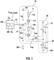
- FIG. 1 shows schematically a simplified block diagram of a device 100 for operating a broadband lambda probe 10 according to preferred embodiments.
- the broadband lambda probe 10 is illustrated here by means of an electrical equivalent circuit diagram and has a Nernst cell 11 and a pump cell 12, which are electrically connected in series with one another via the first circuit node N1.
- the Nernst cell 11 is represented by a voltage source 11a and an internal resistance 11b associated with it
- the pump cell 12 is represented by a voltage source 12a and an internal resistance 12b associated with it.
- the series connection of the Nernst cell 11 and the pump cell 12 has external electrical connections (two-terminal) which are represented by the second circuit node N2 and the third circuit node N3.
- a voltage U N drops across the Nernst cell 11, i.e. between the circuit nodes N2, N1, which can also be referred to as the Nernst voltage
- a voltage Up drops across the pump cell 12, i.e. between the circuit nodes N1, N3, which can also be referred to as the pump voltage.
- the broadband lambda probe 10 has, for example, a structure as shown by way of example in the Figure 1 the EN 10 2013 220 756 A1 is shown.
- the first circuit node N1 may be Fig.1 as the inner pump electrode (“IPE"), the second circuit node N2 as the reference electrode (“RE") and the third Circuit node N3 can be referred to as the outer pumping electrode (“APE").
- IPE inner pump electrode
- RE reference electrode
- APE outer pumping electrode
- a lambda value (combustion air ratio) is determined from an electrical current that flows through the cells 11, 12 by means of the broadband lambda probe 10, particularly in automotive applications.
- the current through the pump cell is regulated, for example by means of a so-called pump current regulator (not shown), such that 450 mV, millivolts, can be measured at the Nernst cell, thus resulting in a Nernst voltage U N of 450 mV at the Nernst cell 11.
- the current can be driven in a positive or negative direction through the probe or its pump cell 12.
- at least one current source can be provided for this purpose.
- a power supply device 20 is provided which is designed to supply the pump cell 12 with an operating current of the desired polarity for operating the broadband lambda probe 10.
- the power supply device 20 has a first current source 21 which is designed to supply the pump cell 12 with an operating current of the first current direction, in particular a positive current Ipos, and a second current source 22 which is designed to supply the pump cell 12 with an operating current of the second current direction (opposite to the first current direction), in particular a negative current Ineg, cf. the correspondingly designated dashed arrows.
- the first current source 21 can thus also be referred to as a "positive current source” 21 and the second current source 22 can thus also be referred to as a "negative current source” 22.
- a (single) positive operating voltage Uchip_supply is provided for operation of the broadband lambda sensor 10, which, in particular in the case of applications in the automotive sector, can be derived from an on-board voltage of the Motor vehicle.
- the two current sources 21, 22 described above are provided in preferred embodiments.
- a reference electrode e.g. in the form of the first circuit node N1 is provided, by means of which currents Ipos, Ineg can be driven in both directions through the pump cell 12, in particular optionally.
- the reference electrode can be connected to the first circuit node N1, which in further preferred embodiments corresponds in particular to a first connection of the pump cell 12.
- a second connection of the pump cell 12 can be connected, in particular optionally, to the current source(s) 21, 22.
- the reference electrode can also be referred to as a "virtual ground electrode”.
- the reference electrode or the first circuit node N1 is temporarily placed at an electrical potential which, for example, corresponds to at least approximately half the operating voltage Uchip_supply ("chip supply"), based on a first reference potential BP1, for example the (real) ground potential.
- both the negative current source 22 and the positive current source 21 can drive currents Ipos, Ineg through the pump cell 12 (optionally, in particular alternately over time).
- the positive operating voltage Uchip_supply with which, for example, the device 100 is also supplied for its operation, is, for example, 5 volts.
- real current sources 21, 22 in further preferred embodiments require a non-vanishing voltage drop Udrop across the (current) source in order to be able to drive a current.
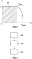
- a current I of a real current source is plotted against a voltage U I.
- a working range of the real current source is shown in Fig. 2 designated with the reference symbol AB, and a supply voltage with the reference symbol Usupply.
- the voltage drop Udrop is, for example, 1 volt (V).
- the operating behavior of at least one of the current sources 21, 22 of the power supply device 20 can be at least approximately described by the diagram of the Fig. 2 to be discribed.
- a current flowing through the pump cell 12 ( Fig.1 ) a voltage.
- this voltage drop across the pump cell 12 can be a maximum of approximately 2.5 V, depending on the configuration of the broadband lambda probe 10 or the pump cell 12.
- the supply voltage for the broadband lambda sensor 10 or the current sources 21, 22 feeding it can therefore be selected to be 7 V, the supply voltage being generated if necessary from the typically available supply voltage Uchip_supply of, for example, 5 V.
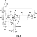
- the device 100 which is hereinafter referred to with reference to Fig.3 described method comprising the following steps: Determining 200 a voltage drop Up ( Fig.1 , "Pump voltage") across the pump cell 12, Determine 202 ( Fig.3 ) of a first setpoint SW ( Fig.1 ) for the electrical potential of the first circuit node N1 as a function of the voltage drop Up across the pump cell 12, loading 204 ( Fig.3 ) of the first circuit node N1 with the first setpoint SW, which in Fig.1 is indicated by the block arrow A1.
- the first circuit node N1 which lies between the Nernst cell 11 and the pump cell 12 or connects these cells 11, 12 to one another, is subjected to an electrical potential corresponding to the first setpoint SW1, which depends on the voltage drop Up across the pump cell.
- This enables efficient use of any electrical supply voltage Uchip_supply that may already be present and efficient operation of one or more current sources 21, 22 for supplying the broadband lambda sensor 10 with an operating current Ipos, Ineg.
- the first circuit node N1 can be optionally placed at different electrical potentials or subjected to different electrical potentials depending on the voltage drop Up across the pump cell 12 (e.g.
- the broadband lambda sensor 10 and/or the power supply device 20 assigned to it and/or the device 100 are operated with a (preferably single) positive supply voltage Uchip_supply of e.g. 5 V.
- Further preferred embodiments advantageously utilize the fact that the voltage Up at the pump cell 12 is positive or negative depending on the operating state (in particular current and gas) of the broadband lambda probe 10, and that thus, in particular depending on the instantaneous air ratio ⁇ , either the positive or the negative current source is active, but not both current sources 21, 22 at the same time.
- this allows the electrical potential of the reference electrode ("virtual ground”), i.e. the first circuit node N1 between the Nernst cell 11 and the pump cell 12, to be made variable in further preferred embodiments, in particular the potential of the first circuit node N1 depending on the current direction and cell voltage Up of the pump cell 12.
- the reference electrode i.e. the first circuit node N1 between the Nernst cell 11 and the pump cell 12
- the process 200, 202, 204 is carried out according to Fig.3 to repeat at least temporarily, in particular to carry out periodically.
- charge transfer currents can occur at (particularly parasitic) capacitances of lines and/or connections and/or other components of the broadband lambda probe such as the Nernst cell and the pump cell ("line, pin and probe capacitances") when the potential of the first circuit node N1 is changed.
- Such charge transfer currents can possibly influence the sensor measurement result of the broadband lambda probe 10. Therefore, in further preferred embodiments, the potential of the first circuit node N1 is changed in particular (preferably only) when there is a need, i.e., for example, when the cell voltage Up of the pump cell 12, for example, becomes so high that the currently active (particularly positive or negative) current source 21, 22 no longer has sufficient voltage drop.
- FIG. 4 shows a schematic block diagram according to further preferred embodiments.
- the broadband lambda sensor 10 is shown, represented by an equivalent circuit diagram of its Nernst cell 11 and its pump cell 12 with the already described circuit nodes N1, N2, N3. Also shown is the power supply device 20, which is connected between a second reference potential BP2 and the first reference potential BP1 (ground potential), the first reference potential BP1 corresponding to the common operating voltage Uchip_supply of 5 V, for example. Further from Fig.4 A capacitive element C EMV is visible.
- an optional trimming resistor which is not described in more detail here, can also be provided between the circuit nodes N3, N4.
- the resistance value of the optional trimming resistor can be set, for example, depending on the tolerance of the lambda sensor. preferably during the manufacture of the lambda sensor or the system containing it.
- the resistance value of the optional trim resistor can be read out or determined for the operation of the lambda sensor and taken into account accordingly when evaluating the measured values.
- a device 14 which is designed to determine the pump voltage Up and for this purpose has, for example, a differential amplifier 14a.
- an analog-digital converter (“ADC") 14b is provided which transforms analog values for the pump voltage Up determined by means of the differential amplifier 14a into the digital domain, in particular into a time- and value-discrete pump voltage signal sup.
- the determination of the first setpoint value SW is carried out as a function of a characteristic curve KL, wherein in particular the characteristic curve KL has a predeterminable dependence of the first setpoint value SW on the voltage drop Up across the pump cell 12.
- the first setpoint SW can be determined from the signal sup, cf. step 202 of Fig.3 , which at Fig.4 for example by means of a characteristic curve KL ⁇ (see also the characteristic curve KL from Fig.1 ) is performed.
- the first setpoint value SW is transformed by means of a digital-analog converter DAC into an analog signal, which corresponds, for example, to the electrical potential corresponding to the first setpoint value SW and is applied to the first circuit node N1.
- this corresponds, for example, to the voltage Uvm.
- the first circuit node N1 can thus be set to a predeterminable electrical potential by means of the voltage Uvm depending on the voltage drop Up across the pump cell 12, which can change in particular during operation of the broadband lambda sensor 10 (in particular depending on the voltage drop Up across the pump cell 12), whereby a reliable measurement of the Air ratio can be determined by means of the broadband lambda probe 10.
- efficient operation of the broadband lambda probe 10 and the device 100 ( Fig.1 ) with a single common supply voltage Uchip_supply is possible.
- one or more, preferably all, of the components 14, 14a, 14b, KL, KL ⁇ , DAC are integrated into the device 100 ( Fig.1 ), in particular arranged on a common semiconductor substrate.
- the characteristic curve KL, KL ⁇ can also be obtained from an external source (eg connected microcontroller).
- the dependence of the potential of the first circuit node N1 on the pump voltage Up is controlled via a characteristic curve KL, KL ⁇ , in particular digitally, e.g. using a computing device which evaluates the characteristic curve KL, KL ⁇ as a function of a value determined (e.g. by means of the ADC 14b) for the instantaneous voltage drop at the pump cell 12 in order to determine the first setpoint value SW.
- the first setpoint SW ( Fig.1 ) is assigned a constant first value W1
- the curve K which can be used as characteristic curve KL, KL ⁇ in further preferred embodiments.
- the curve K represents a setpoint SWP for the potential of the first circuit node N1 as a function of the pump voltage Up.
- the first value range WB1 can be as in Fig.5 shown a coherent range of values, which in this case comprises a first subrange WB1a (positive values of the pump voltage Up ( Fig.1 ) or use of a positive operating current Ipos for the operation of the pump cell 12) and a second sub-area WB1b (negative values of the pump voltage Up ( Fig.1 ) or use of a negative operating current Ineg for the operation of the pump cell 12).
- the first value range WB1 can also be a non-contiguous value range (not shown), thus having several partial areas that are not directly adjacent to one another.
- a second value W2 which is variable depending on the value of the voltage drop Up is assigned to the first setpoint value SW.
- the second value range WB2 can be a continuous value range (not shown).
- the second value range WB2 can be a non-continuous value range, thus having several sub-ranges WB2a, WB2b.
- the second value W2 is linearly variable depending on the value of the voltage drop Up, wherein in particular a slope of the linear change of the second value depending on the value of the voltage drop is negative, in particular has the value -1.
- the potential of the first circuit node N1 can thus be reduced, for example with increasing voltage drop Up at the pump cell 12, to an extent corresponding to the slope, whereby reliable operation of the broadband lambda sensor 10 and in particular also of the currently active power source 21 or 22 is always ensured, in particular although the possibly only existing positive supply voltage Uchip_supply for the broadband lambda sensor 10 and the power sources 21, 22 is comparatively small, e.g. 5 volts.
- a third value W3 that changes depending on the value of the voltage drop Up is assigned to the first setpoint value SW.
- the third value range WB3 can be a continuous value range (not shown).
- the third value range WB3 can be a non-continuous value range, thus having several sub-ranges WB3a, WB3b.
- the third value W3 is linearly variable depending on the value of the voltage drop Up, wherein in particular a slope of the linear change of the third value W3 depending on the value of the voltage drop Up is positive, in particular has the value 1.
- the potential of the first circuit node can thus be increased, e.g. with increasing voltage drop Up at the pump cell 12, to an extent corresponding to the slope, whereby reliable operation of the broadband lambda sensor 10 and in particular also of the currently active current source 21 or 22 is always ensured.
- Figure 6 shows schematically a simplified block diagram of a device 1000 according to further preferred embodiments.
- the device 100 can be made of Fig.1 the configuration 1000 according to Fig.6
- the device 1000 has at least one computing device 1002, at least one memory device 1004 assigned to the computing device 1002 for at least temporarily storing a computer program PRG, wherein the computer program PRG is designed in particular for controlling an operation of the device 100, 1000 and/or for carrying out the method according to the embodiments.
- the computing device 1002 has at least one of the following elements: a microprocessor, a microcontroller, a digital signal processor (DSP), a programmable logic module (eg FPGA, field programmable gate array), an ASIC (application specific integrated circuit). Combinations of these are also conceivable in further preferred embodiments.
- DSP digital signal processor
- FPGA field programmable gate array
- ASIC application specific integrated circuit
- the memory device 1004 has at least one of the following elements: a volatile memory 1004a, in particular random access memory (RAM), a non-volatile memory 1004b, in particular flash EEPROM.
- the computer program PRG is preferably stored in the non-volatile memory 1004b.
- the characteristic curve KL, KL ⁇ ( Fig.1 , 4 ) can be stored in the storage device 1004, preferably in such a way that it can be changed, in particular dynamically (during the running time of the device), e.g. adapted to a target system (e.g. broadband lambda probe 10 or an exhaust aftertreatment system having at least one lambda probe 10 and/or a power supply device 20 therefor or the like).
- a target system e.g. broadband lambda probe 10 or an exhaust aftertreatment system having at least one lambda probe 10 and/or a power supply device 20 therefor or the like.
- the device 1000 has an interface device 1006, which can have one or more of the components 14, 14a, 14b, KL, KL ⁇ , DAC or can implement their functionality or has and/or implements them.
- a pump cell voltage-dependent potential setting of the first circuit node N1 (which can also be referred to as “virtual ground”) can advantageously be carried out, in particular using a characteristic curve KL.
- an (in particular "standard”) operating voltage Uchip_supply can advantageously be used for the control unit 100, 1000 or other control units and at the same time a sufficient voltage drop is available for the current source(s) 21, 22 even at high probe voltages or pump voltages Up. This saves costs because complex battery voltage conditioning, e.g. for a separate voltage supply with a higher voltage (e.g. > 5 V), is not required.
- the current sources 21, 22 can also be manufactured more cost-effectively than in conventional systems, since for the realization of the current sources 21, 22, in particular when integrated into a semiconductor component, in particular the computing device 100, 1000 (eg in the interface module 1006 of Fig.6 ) no high-voltage transistors are necessary.
- the device 100, 1000 can be operated reliably, in particular with a weak (vehicle) battery, e.g. down to battery voltages of 6V, since the comparatively small (only) required supply voltage Uchip_supply of e.g. 5V can still be reliably provided in such cases, in particular can be derived from the battery voltage.
- the electrical potential of the first circuit node N1 i.e. the virtual ground
- the constant value W1 of the curve K in the first value range WB1 so that a measurement result of the broadband lambda sensor 10 is not disturbed.
- a further advantage of further preferred embodiments is that the fact can be exploited that the current sources 21, 22 reduce the current when there is no longer sufficient voltage drop (Udrop too small) at the sources (see also Fig. 2 ).
- the characteristic curve K, KL, KL ⁇ in further preferred embodiments, excessive voltages on the broadband lambda sensor 10 and thus damage/blackening of the sensor can be avoided ("blackening protection").
- steps 200, 202, 204 are performed according to Fig.3 then, preferably always, when the pump voltage Up changes.
- a pump voltage regulator (not shown) is provided, which may change the operating current for the pump cell 12, the Execution of steps 200, 202, 204 can be coupled, for example, to an operating cycle of the pump voltage regulator. This ensures that the electrical potential of the first circuit node N1 or the voltage Uvm is always adjusted when the pump voltage Up changes, i.e. preferably in the same cycle as the pump current is changed.
- Up + Udrop- + Uvm ⁇ Uchip_supply e.g. for positive pump voltage Up
- + Udrop- ⁇ Uvm for negative pump voltage Up
- Up + Udrop- ⁇ Uvm for negative pump voltage Up
- Uvm can be adjusted according to further preferred embodiments, in particular linearly, preferably with a slope of 1, whereby the above "Condition 1" can be fulfilled.
- a correction of charge reversal currents such as those occurring at the EMC capacitor C EMV ( Fig.4 ) as a result of the change in the potential of the first circuit node N1. If, for example, the potential of the first circuit node N1 or the voltage Uvm is changed, the charge of the EMC capacitor C EMV changes, which leads to a current flow in the capacitor C EMV .
- the device 100, 1000 is designed to measure this ("VM") current and to determine the value of the air ratio ⁇ from this.
- C is the pin capacitance to ground
- dU is the change in the potential or voltage Uvm at the first circuit node N1 within the cycle
- dt is the cycle duration.
- the calculated current I can then advantageously be subtracted from the current Ivm flowing through the first circuit node N1, which can also be measured, in order to determine the pumping current of the probe 10.
- an influence on the Nernst voltage regulator is not to be expected, since the Nernst voltage U N is preferably determined differentially between the circuit nodes N3, N1.
- the characteristic curve K, KL, KL ⁇ can be designed as follows:
Landscapes
- Engineering & Computer Science (AREA)
- Chemical & Material Sciences (AREA)
- Health & Medical Sciences (AREA)
- Life Sciences & Earth Sciences (AREA)
- Biochemistry (AREA)
- Immunology (AREA)
- Physics & Mathematics (AREA)
- Analytical Chemistry (AREA)
- Chemical Kinetics & Catalysis (AREA)
- General Health & Medical Sciences (AREA)
- General Physics & Mathematics (AREA)
- Electrochemistry (AREA)
- Pathology (AREA)
- Molecular Biology (AREA)
- Combustion & Propulsion (AREA)
- Mechanical Engineering (AREA)
- General Engineering & Computer Science (AREA)
- Measurement Of Current Or Voltage (AREA)
- Semiconductor Integrated Circuits (AREA)
Description
- Die Offenbarung betrifft ein Verfahren zum Betreiben einer Breitband-Lambdasonde, bei der eine Nernstzelle und eine Pumpzelle über einen ersten Schaltungsknotenpunkt elektrisch in Serie geschaltet sind.
- Die Offenbarung betrifft ferner eine Vorrichtung zum Betreiben einer Breitband-Lambdasonde, bei der eine Nernstzelle und eine Pumpzelle über einen ersten Schaltungsknotenpunkt elektrisch in Serie geschaltet sind.
WO 01 /96851 A1 - Bevorzugte Ausführungsformen beziehen sich auf
ein Verfahren zum Betreiben einer Breitband-Lambdasonde gemäß Anspruch 1. Dadurch wird der erste Schaltungsknotenpunkt, der zwischen der Nernstzelle und der Pumpzelle liegt bzw. diese Zellen miteinander verbindet, mit einem dem ersten Sollwert entsprechenden elektrischen Potential, das von dem Spannungsabfall über der Pumpzelle abhängt, beaufschlagt. Dies ermöglicht eine effiziente Nutzung einer ggf. bereits vorhandenen elektrischen Versorgungsspannung und einen effizienten Betrieb von einer oder mehreren Stromquellen zur Versorgung der Breitband-Lambdasonde mit einem Betriebsstrom. - Bei weiteren bevorzugten Ausführungsformen weist die Breitband-Lambdasonde beispielsweise einen Aufbau auf, wie er beispielhaft in der
Figur 1 derDE 10 2013 220 756 A1 gezeigt ist. - Bei weiteren bevorzugten Ausführungsformen wird mittels der Breitband-Lambdasonde, insbesondere bei Anwendungen im Kraftfahrzeugbereich, ein Lambdawert (Verbrennungsluftverhältnis) aus einem elektrischen Strom, der durch die Zellen (Nernstzelle und Pumpzelle) fließt, ermittelt. Bei weiteren bevorzugten Ausführungsformen wird der Strom durch die Pumpzelle dabei z.B. mittels eines sog. Pumpstromreglers so eingeregelt, dass an der Nernstzelle z.B. 450 mV, Millivolt, gemessen werden kann, mithin eine Nernstspannung von z.B. 450 mV an der Nernstzelle abfällt. Je nachdem, ob fettes oder mageres Abgas an der Breitband-Lambdasonde anliegt, kann gemäß weiteren bevorzugten Ausführungsformen der Strom in positiver oder negativer Richtung durch die Sonde getrieben werden. Hierfür kann bei weiteren bevorzugten Ausführungsformen wenigstens eine Stromquelle vorgesehen sein.
- Bei weiteren bevorzugten Ausführungsformen wird für einen Betrieb der Breitband-Lambdasonde eine (einzige) positive Betriebsspannung bereitgestellt, die insbesondere bei Anwendungen im Kraftfahrzeugbereich beispielsweise aus einer Bordnetzspannung des Kraftfahrzeugs ableitbar ist. Um dennoch die Breitband-Lambdasonde je nach Betriebszustand mit einem positiven oder einem negativen Betriebsstrom versorgen zu können, sind bei weiteren bevorzugten Ausführungsformen zwei Stromquellen (eine "negative Stromquelle", die dazu ausgebildet ist, einen negativen Strom durch die Pumpzelle zu treiben, und eine "positive Stromquelle", die dazu ausgebildet ist, einen positiven Strom durch die Pumpzelle zu treiben) und eine Bezugselektrode vorgesehen, mittels derer, insbesondere wahlweise, Ströme in beide Richtungen durch die Pumpzelle getrieben werden können. Hierzu ist die Bezugselektrode bei weiteren bevorzugten Ausführungsformen mit dem ersten Schaltungsknotenpunkt verbindbar, der bei weiteren bevorzugten Ausführungsformen insbesondere einem ersten Anschluss der Pumpzelle entspricht. Ein zweiter Anschluss der Pumpzelle ist bei weiteren bevorzugten Ausführungsformen, insbesondere wahlweise, mit der bzw. den Stromquellen verbindbar. Die Bezugselektrode kann bei weiteren bevorzugten Ausführungsformen auch als "virtuelle Masseelektrode" bezeichnet werden.
- Bei weiteren bevorzugten Ausführungsformen ist vorgesehen, dass die Bezugselektrode zeitweise auf ein elektrisches Potential gelegt wird, das z.B. zumindest etwa einer halben Spannung der vorstehend genannten einen (insbesondere einzigen) positiven Betriebsspannung ("Chip-Versorgung"), bezogen auf ein erstes Bezugspotential, beispielsweise das (reale) Massepotential, entspricht. Somit kann sowohl die negative Stromquelle, als auch die positive Stromquelle Ströme durch die Zelle treiben. Bei weiteren bevorzugten Ausführungsformen ist vorgesehen, dass die positive Betriebsspannung ("Chip-Versorgung") z.B. 5 V (Volt) beträgt.
- Untersuchungen der Anmelderin zufolge benötigen reale Stromquellen bei weiteren bevorzugten Ausführungsformen einen nichtverschwindenden Spannungsabfall Udrop über der (Strom-)Quelle, um einen Strom treiben zu können. Bei weiteren bevorzugten Ausführungsformen beträgt der Spannungsabfall Udrop beispielsweise 1 V.
- Weiteren Untersuchungen der Anmelderin zufolge weist die Pumpzelle der Breitband-Lambdasonde eine Spannungsquelle mit einem zugehörigen Innenwiderstand auf bzw. kann als Spannungsquelle mit einem zugehörigen Innenwiderstand aufgefasst bzw. modelliert werden. Dadurch fällt bei einem Stromfluss durch die Pumpzelle eine Spannung ab. Bei weiteren bevorzugten Ausführungsformen kann dieser Spannungsabfall über der Pumpzelle je nach Art und/oder Betrieb und/oder Konfiguration der Breitband-Lambdasonde bzw. der Pumpzelle maximal etwa 2,5 V betragen.
- Bei weiteren bevorzugten Ausführungsformen ist vorgesehen, dass, insbesondere im Falle eines negativen Betriebsstroms bzw. Pumpstroms durch die Pumpzelle, die Spannung Uvm an der Bezugselektrode, bezogen auf das erste Bezugspotential, insbesondere Massepotential, größer gleich einer Summe aus dem Spannungsabfall Up- an der Pumpzelle (im Falle des negativen Betriebsstroms) und dem Spannungsabfall Udrop- an der negativen Stromquelle ist, Uvm >= Up- + Udrop-, wodurch sichergestellt ist, dass die (reale) negative Stromquelle einen Strom treiben kann.
- Bei weiteren bevorzugten Ausführungsformen ist vorgesehen, dass, insbesondere im Falle eines positiven Betriebsstroms bzw. Pumpstroms durch die Pumpzelle, die Spannung Uvm an der Bezugselektrode, bezogen auf das erste Bezugspotential, insbesondere Massepotential, kleiner gleich einer Differenz aus der (insbesondere einzigen) positiven Betriebsspannung Uchip_supply, dem Spannungsabfall Up+ an der Pumpzelle (im Falle des positiven Betriebsstroms) und dem Spannungsabfall Udrop+ an der positiven Stromquelle ist, Uvm <= Uchip_supply - Udrop+ - Up+, wodurch sichergestellt ist, dass die (reale) positive Stromquelle einen Strom treiben kann.
- Bei weiteren bevorzugten Ausführungsformen kann für den Betrieb der Breitband-Lambdasonde sowohl mit negativem als auch mit positivem Betriebsstrom - unter Verwendung der vorstehend beispielhaft genannten Werte für die Spannungsabfälle - die positive Versorgungspannung wie folgt gewählt werden: Up- + Udrop- = Uchip_supply - Udrop+ - Up+, was auf Uchip_supply = Up- + Udrop- - Udrop+ - Up+ führt, also mit o.g. Beispielwerten: Uchip_supply = 2,5 V + 1 V + 1 V + 2,5 V = 7 V, was ersichtlich höher ist als eine typischerweise verfügbare Versorgungsspannung für Recheneinrichtungen von z.B. 5 Volt. Bei weiteren bevorzugten Ausführungsformen kann demnach die Versorgungsspannung für die Breitband-Lambdasonde bzw. die sie speisenden Stromquellen (insbesondere positiv und negativ) zu 7 V gewählt werden, wobei die Versorgungsspannung ggf. aus der typischerweise verfügbaren Versorgungsspannung von z.B. 5 V erzeugt wird.
- Bei weiteren bevorzugten Ausführungsformen ist demgegenüber wie bereits eingangs beschrieben, vorgesehen, zumindest zeitweise das nachfolgende Verfahren auszuführen: Ermitteln eines Spannungsabfalls über der Pumpzelle, Ermitteln eines ersten Sollwerts für das elektrische Potential des ersten Schaltungsknotenpunkts in Abhängigkeit des Spannungsabfalls über der Pumpzelle, Beaufschlagen des ersten Schaltungsknotenpunkts mit dem ersten Sollwert. Gegenüber einem permanenten Belassen des ersten Schaltungsknotenpunkts auf einem konstanten elektrischen Potential, das z.B. der halben Versorgungsspannung entspricht, kann somit gemäß bevorzugten Ausführungsformen der erste Schaltungsknotenpunkt in Abhängigkeit von der Spannungsabfall über der Pumpzelle wahlweise auf verschiedene elektrische Potentiale gelegt bzw. mit verschiedenen elektrischen Potentialen beaufschlagt werden. Dies ermöglicht vorteilhaft die Nutzung einer (einzigen) positiven Versorgungsspannung von z.B. 5 V und ermöglicht ferner gleichzeitig, dennoch genug Spannung für einen zuverlässigen Betrieb der Breitband-Lambdasonde und die ihr zugeordneten Stromquellen bereitstellen.
- Weitere bevorzugten Ausführungsformen nutzen vorteilhaft aus, dass die Spannung an der Pumpzelle je nach Betriebszustand (insbesondere Strom und Gas) der Breitband-Lambdasonde positiv oder negativ ist, und dass somit insbesondere je nach der momentanen Luftzahl λ entweder die positive oder die negative Stromquelle aktiv ist, nicht jedoch beide Stromquellen gleichzeitig. Dies erlaubt Untersuchungen der Anmelderin zufolge, bei weiteren bevorzugten Ausführungsformen das elektrische Potential der Bezugselektrode ("virtuelle Masse"), also des ersten Schaltungsknotenpunkts zwischen der Nernstzelle und der Pumpzelle, variabel zu gestalten, insbesondere das Potential des ersten Schaltungsknotenpunkts je nach Stromrichtung und Zellspannung der Pumpzelle zu verändern.
- Weiteren Untersuchungen der Anmelderin zufolge, kann es an (insbesondere parasitären) Kapazitäten von Leitungen und/oder Anschlüssen und/oder sonstigen Komponenten der Breitband-Lambdasonde wie z.B. der Nernstzelle und der Pumpzelle ("Leitungs-, Pin- und Sondenkapazitäten") zu Umladeströmen kommen, wenn das Potential des ersten Schaltungsknotenpunkts verändert wird. Solche Umladeströme können u.U. das Sensormessergebnis der Breitband-Lambdasonde beeinflussen. Daher ist bei weiteren bevorzugten Ausführungsformen vorgesehen, das Potential des ersten Schaltungsknotenpunkts insbesondere dann (vorzugsweise nur dann) zu verändern, wenn auch Bedarf besteht, also z.B. dann, wenn die Zellspannung z.B. der Pumpzelle so groß wird, dass die momentan aktive (insbesondere positive oder negative) Stromquelle nicht mehr genügend Spannungsabfall hat.
- Bei weiteren bevorzugten Ausführungsformen ist vorgesehen, dass das Ermitteln des ersten Sollwerts in Abhängigkeit einer Kennlinie ausgeführt wird, wobei insbesondere die Kennlinie eine vorgebbare Abhängigkeit des ersten Sollwerts von dem Spannungsabfall über der Pumpzelle aufweist.
- Bei weiteren bevorzugten Ausführungsformen ist vorgesehen, dass die Abhängigkeit des Potentials des ersten Schaltungsknotenpunkts von der Pumpspannung über eine bzw. die Kennlinie gesteuert wird, insbesondere digital, z.B. unter Verwendung einer Recheneinrichtung, die die Kennlinie in Abhängigkeit eines ermittelten Werts für den momentanen Spannungsabfall an der Pumpzelle auswertet, um den ersten Sollwert zu ermitteln.
- Es ist vorgesehen, dass für einen ersten Wertebereich des Spannungsabfalls über der Pumpzelle dem ersten Sollwert ein, insbesondere konstanter, erster Wert zugeordnet wird. Bei weiteren bevorzugten Ausführungsformen kann der erste Wertebereich ein zusammenhängender Wertebereich sein. Bei weiteren bevorzugten Ausführungsformen kann der erste Wertebereich ein nicht zusammenhängender Wertebereich sein, mithin mehrere Teilbereiche aufweisen. Damit kann beispielsweise bewirkt werden, dass in einem Bereich um λ = 1 (z.B. entsprechend dem ersten Wertebereich) das Potential des ersten Schaltungsknotenpunkts fix bleibt, da in diesem Bereich der Spannungsabfall an der Pumpzelle nicht groß ist.
- Es ist vorgesehen, dass für einen zweiten Wertebereich des Spannungsabfalls über der Pumpzelle dem ersten Sollwert ein in Abhängigkeit des Werts des Spannungsabfalls, veränderlicher zweiter Wert zugeordnet wird. Bei weiteren bevorzugten Ausführungsformen kann der zweite Wertebereich ein zusammenhängender Wertebereich sein. Bei weiteren bevorzugten Ausführungsformen kann der zweite Wertebereich ein nicht zusammenhängender Wertebereich sein, mithin mehrere Teilbereiche aufweisen. Durch den veränderlichen zweiten Wert kann vorteilhaft eine Anpassung des Potentials des ersten Schaltungsknotenpunkts an einen gegenüber z.B. dem Betriebszustand λ = 1 veränderten Betriebszustand erfolgen.
- Bei weiteren bevorzugten Ausführungsformen ist vorgesehen, dass der zweite Wert in Abhängigkeit des Werts des Spannungsabfalls linear veränderlich ist, wobei insbesondere eine Steigung der linearen Veränderung des zweiten Werts in Abhängigkeit des Werts des Spannungsabfalls negativ ist, insbesondere den Wert -1 aufweist. Damit kann das Potential des ersten Schaltungsknotenpunkts z.B. mit steigendem Spannungsabfall an der Pumpzelle in einem der Steigung entsprechenden Maß verringert werden, wodurch stets ein zuverlässiger Betrieb der Breitband-Lambdasonde und insbesondere auch der aktuell aktiven Stromquelle sichergestellt ist, insbesondere obwohl die ggf. einzige vorhandene positive Versorgungsspannung für die Breitband-Lambdasonde und die Stromquellen vergleichsweise klein ist, z.B. 5 Volt.
- Bei weiteren bevorzugten Ausführungsformen ist vorgesehen, dass für einen dritten Wertebereich des Spannungsabfalls über der Pumpzelle dem ersten Sollwert ein in Abhängigkeit des Werts des Spannungsabfalls veränderlicher dritter Wert zugeordnet wird. Bei weiteren bevorzugten Ausführungsformen kann der dritte Wertebereich ein zusammenhängender Wertebereich sein. Bei weiteren bevorzugten Ausführungsformen kann der dritte Wertebereich ein nicht zusammenhängender Wertebereich sein, mithin mehrere Teilbereiche aufweisen. Bei weiteren bevorzugten Ausführungsformen ist vorgesehen, dass der dritte Wert in Abhängigkeit des Werts des Spannungsabfalls linear veränderlich ist, wobei insbesondere eine Steigung der linearen Veränderung des dritten Werts in Abhängigkeit des Werts des Spannungsabfalls positiv ist, insbesondere den Wert 1 aufweist. Damit kann das Potential des ersten Schaltungsknotenpunkts z.B. mit steigendem Spannungsabfall an der Pumpzelle in einem der Steigung entsprechenden Maß erhöht werden, wodurch stets ein zuverlässiger Betrieb der Breitband-Lambdasonde und insbesondere auch der aktuell aktiven Stromquelle sichergestellt ist.
- Weitere bevorzugte Ausführungsformen beziehen sich auf eine Vorrichtung zum Betreiben einer Breitband-Lambdasonde gemäß Anspruch 6.
- Bei weiteren bevorzugten Ausführungsformen ist die Vorrichtung zur Ausführung des Verfahrens gemäß den Ausführungsformen ausgebildet.
- Bei weiteren bevorzugten Ausführungsformen weist die Vorrichtung eine Recheneinrichtung und eine der Recheneinrichtung zugeordnete Speichereinrichtung auf, wobei die Vorrichtung dazu ausgebildet ist, eine bzw. die Kennlinie, die eine vorgebbare Abhängigkeit des ersten Sollwerts von dem Spannungsabfall über der Pumpzelle aufweist, zumindest zeitweise mittels der Speichereinrichtung zu speichern.
- Weitere Merkmale, Anwendungsmöglichkeiten und Vorteile der Erfindung ergeben sich aus der nachfolgenden Beschreibung von Ausführungsbeispielen der Erfindung, die in den Figuren der Zeichnung dargestellt sind. Der Schutzumfang der Erfindung wird durch die beigefügten Ansprüche definiert.
- In der Zeichnung zeigt:
- Figur 1
- schematisch ein vereinfachtes Blockdiagramm einer Vorrichtung gemäß bevorzugten Ausführungsformen,
- Figur 2
- schematisch einen Strom einer Stromquelle gemäß weiteren bevorzugten Ausführungsformen aufgetragen über einer Spannung,
- Figur 3
- schematisch ein vereinfachtes Flussdiagramm eines Verfahrens gemäß weiteren bevorzugten Ausführungsformen,
- Figur 4
- schematisch ein vereinfachtes Blockdiagramm einer Vorrichtung gemäß weiteren bevorzugten Ausführungsformen,
- Figur 5
- schematisch eine Kennlinie gemäß weiteren bevorzugten Ausführungsformen, und
- Figur 6
- schematisch ein vereinfachtes Blockdiagramm einer Vorrichtung gemäß weiteren bevorzugten Ausführungsformen.
-
Figur 1 zeigt schematisch ein vereinfachtes Blockdiagramm einer Vorrichtung 100 zum Betreiben einer Breitband-Lambdasonde 10 gemäß bevorzugten Ausführungsformen. Die Breitband-Lambdasonde 10 ist vorliegend mittels eines elektrischen Ersatzschaltbilds illustriert und weist eine Nernstzelle 11 und eine Pumpzelle 12 auf, die über den ersten Schaltungsknotenpunkt N1 elektrisch zueinander in Serie geschaltet sind. Vorliegend ist die Nernstzelle 11 durch eine Spannungsquelle 11a und einen ihr zugeordneten Innenwiderstand 11b repräsentiert, und die Pumpzelle 12 ist durch eine Spannungsquelle 12a und einen ihr zugeordneten Innenwiderstand 12b repräsentiert. - Wie ebenfalls aus
Fig. 1 ersichtlich, weist die Serienschaltung der Nernstzelle 11 und der Pumpzelle 12 äußere elektrische Anschlüsse (Zweipol) auf, die durch den zweiten Schaltungsknotenpunkt N2 und den dritten Schaltungsknotenpunkt N3 repräsentiert sind. Im Betrieb fällt an der Nernstzelle 11, also zwischen den Schaltungsknotenpunkten N2, N1, eine Spannung UN ab, die auch als Nernstspannung bezeichnet werden kann, und an der Pumpzelle 12, also zwischen den Schaltungsknotenpunkten N1, N3, fällt eine Spannung Up ab, die auch als Pumpspannung bezeichnet werden kann. - Bei weiteren bevorzugten Ausführungsformen weist die Breitband-Lambdasonde 10 beispielsweise einen Aufbau auf, wie er beispielhaft in der
Figur 1 derDE 10 2013 220 756 A1 gezeigt ist. - Bei weiteren bevorzugten Ausführungsformen kann der erste Schaltungsknotenpunkt N1 gemäß
Fig. 1 als innere Pumpelektrode ("IPE"), der zweite Schaltungsknotenpunkt N2 als Referenzelektrode ("RE") und der dritte Schaltungsknotenpunkt N3 als äußere Pumpelektrode ("APE") bezeichnet werden. - Bei weiteren bevorzugten Ausführungsformen wird mittels der Breitband-Lambdasonde 10, insbesondere bei Anwendungen im Kraftfahrzeugbereich, ein Lambdawert (Verbrennungsluftverhältnis) aus einem elektrischen Strom, der durch die Zellen 11, 12 fließt, ermittelt. Bei weiteren bevorzugten Ausführungsformen wird der Strom durch die Pumpzelle dabei z.B. mittels eines sog. Pumpstromreglers (nicht gezeigt) so eingeregelt, dass an der Nernstzelle 450 mV, Millivolt, gemessen werden kann, mithin einen Nernstspannung UN von 450 mV an der Nernstzelle 11 abfällt. Je nachdem, ob fettes oder mageres Abgas an der Breitband-Lambdasonde 10 anliegt, kann gemäß weiteren bevorzugten Ausführungsformen der Strom in positiver oder negativer Richtung durch die Sonde bzw. ihre Pumpzelle 12 getrieben werden. Hierfür kann bei weiteren bevorzugten Ausführungsformen wenigstens eine Stromquelle vorgesehen sein.
- Bei weiteren bevorzugten Ausführungsformen ist eine Stromversorgungseinrichtung 20 vorgesehen, die dazu ausgebildet ist, die Pumpzelle 12 für den Betrieb der Breitband-Lambdasonde 10 mit einem Betriebsstrom gewünschter Polarität zu bestromen. Hierzu weist die Stromversorgungseinrichtung 20 bei weiteren bevorzugten Ausführungsformen eine erste Stromquelle 21 auf, die dazu ausgebildet ist, die Pumpzelle 12 mit einem Betriebsstrom erster Stromrichtung, insbesondere einem positiven Strom Ipos, zu bestromen, und eine zweite Stromquelle 22, die dazu ausgebildet ist, die Pumpzelle 12 mit einem Betriebsstrom zweiter Stromrichtung (entgegengesetzt zu der ersten Stromrichtung), insbesondere einem negativen Strom Ineg, zu bestromen, vgl. die entsprechend bezeichneten gestrichelten Pfeile. Bei weiteren bevorzugten Ausführungsformen kann die erste Stromquelle 21 somit auch als "positive Stromquelle" 21 und die zweite Stromquelle 22 somit auch als negative Stromquelle" 22 bezeichnet werden.
- Bei weiteren bevorzugten Ausführungsformen wird für einen Betrieb der Breitband-Lambdasonde 10 eine (einzige) positive Betriebsspannung Uchip_supply bereitgestellt, die insbesondere bei Anwendungen im Kraftfahrzeugbereich beispielsweise aus einer Bordnetzspannung des Kraftfahrzeugs ableitbar ist. Um dennoch die Breitband-Lambdasonde 10 je nach Betriebszustand mit einem positiven oder einem negativen Betriebsstrom Ipos, Ineg versorgen zu können, sind bei bevorzugten Ausführungsformen die beiden vorstehend beschriebenen Stromquellen 21, 22 vorgesehen. Zusätzlich ist bei weiteren bevorzugten Ausführungsformen eine Bezugselektrode (z.B. in Form des ersten Schaltungsknotenpunkts N1) vorgesehen, mittels der, insbesondere wahlweise, Ströme Ipos, Ineg in beide Richtungen durch die Pumpzelle 12 getrieben werden können. Hierzu ist die Bezugselektrode bei weiteren bevorzugten Ausführungsformen mit dem ersten Schaltungsknotenpunkt N1 verbindbar, der bei weiteren bevorzugten Ausführungsformen insbesondere einem ersten Anschluss der Pumpzelle 12 entspricht. Ein zweiter Anschluss der Pumpzelle 12 ist bei weiteren bevorzugten Ausführungsformen, insbesondere wahlweise, mit der bzw. den Stromquellen 21, 22 verbindbar. Die Bezugselektrode kann bei weiteren bevorzugten Ausführungsformen auch als "virtuelle Masseelektrode" bezeichnet werden.
- Bei weiteren bevorzugten Ausführungsformen ist vorgesehen, dass die Bezugselektrode bzw. der erste Schaltungsknotenpunkt N1 zeitweise auf ein elektrisches Potential gelegt wird, das z.B. zumindest etwa der halben Betriebsspannung Uchip_supply ("Chip-Versorgung"), bezogen auf ein erstes Bezugspotential BP1, beispielsweise das (reale) Massepotential, entspricht. Somit kann sowohl die negative Stromquelle 22, als auch die positive Stromquelle 21 (wahlweise, insbesondere zeitlich abwechselnd) Ströme Ipos, Ineg durch die Pumpzelle 12 treiben. Bei weiteren bevorzugten Ausführungsformen ist vorgesehen, dass die positive Betriebsspannung Uchip_supply, mit der z.B. auch die Vorrichtung 100 für ihren Betrieb versorgt wird, z.B. 5 Volt beträgt.
- Untersuchungen der Anmelderin zufolge benötigen reale Stromquellen 21, 22 bei weiteren bevorzugten Ausführungsformen einen nichtverschwindenden Spannungsabfall Udrop über der (Strom-)Quelle, um einen Strom treiben zu können. Dies ist schematisch in
Fig. 2 gezeigt, in der ein Strom I einer realen Stromquelle über einer Spannung UI aufgetragen ist. Ein Arbeitsbereich der realen Stromquelle ist inFig. 2 mit dem Bezugszeichen AB bezeichnet, und eine Versorgungsspannung mit dem Bezugszeichen Usupply. AusFig. 2 ist ersichtlich, dass sich, ausgehend von einem Strom I=0 bei der Spannung Usupply, der genannte Spannungsabfall Udrop einstellt, wenn der Strom I bis zu dem Zielwert IT ansteigt. Bei weiteren bevorzugten Ausführungsformen beträgt der Spannungsabfall Udrop beispielsweise 1 Volt (V). Bei weiteren bevorzugten Ausführungsformen kann beispielsweise das Betriebsverhalten wenigstens einer der Stromquellen 21, 22 der Stromversorgungseinrichtung 20 zumindest näherungsweise durch das Diagramm derFig. 2 beschrieben werden. - Weiteren Untersuchungen der Anmelderin zufolge fällt bei einem Stromfluss durch die Pumpzelle 12 (
Fig. 1 ) eine Spannung ab. Bei weiteren bevorzugten Ausführungsformen kann dieser Spannungsabfall über dem Pumpzelle 12 je nach Konfiguration der Breitband-Lambdasonde 10 bzw. der Pumpzelle 12 maximal etwa 2,5 V betragen. - Bei weiteren bevorzugten Ausführungsformen ist vorgesehen, dass, insbesondere im Falle eines negativen Betriebsstroms bzw. Pumpstroms Ineg durch die Pumpzelle 12, die Spannung Uvm an der Bezugselektrode bzw. dem ersten Schaltungsknotenpunkt N1, bezogen auf das erste Bezugspotential BP1, insbesondere Massepotential, größer gleich einer Summe aus dem Spannungsabfall Up- an der Pumpzelle 12 (im Falle des negativen Betriebsstroms Ineg) und dem Spannungsabfall Udrop- an der negativen Stromquelle 22 ist, Uvm >= Up- + Udrop-, wodurch sichergestellt ist, dass die (reale) negative Stromquelle 22 einen Strom treiben kann.
- Bei weiteren bevorzugten Ausführungsformen ist vorgesehen, dass, insbesondere im Falle eines positiven Betriebsstroms bzw. Pumpstroms Ipos durch die Pumpzelle 12, die Spannung Uvm an der Bezugselektrode bzw. dem ersten Schaltungsknotenpunkt N1, bezogen auf das erste Bezugspotential BP1, insbesondere Massepotential, kleiner gleich einer Differenz aus der (insbesondere einzigen) positiven Betriebsspannung Uchip_supply, dem Spannungsabfall Up+ an der Pumpzelle 12 (im Falle des positiven Betriebsstroms) und dem Spannungsabfall Udrop+ an der positiven Stromquelle 21 ist, Uvm <= Uchip_supply - Udrop+ - Up+, wodurch sichergestellt ist, dass die (reale) positive Stromquelle 21 einen Strom treiben kann.
- Bei weiteren bevorzugten Ausführungsformen kann für den Betrieb der Breitband-Lambdasonde 10 sowohl mit negativem als auch mit positivem Betriebsstrom - unter Verwendung der vorstehend beispielhaft genannten Werte für die Spannungsabfälle - die positive Versorgungspannung wie folgt gewählt werden: Up- + Udrop- = Uchip_supply - Udrop+ - Up+, was auf Uchip_supply = Up- + Udrop- - Udrop+ - Up+ führt, also mit o.g. Beispielwerten: Uchip_supply = 2,5 V + 1 V + 1 V + 2,5 V = 7 V, was ersichtlich höher ist als eine typischerweise verfügbare Versorgungsspannung für Recheneinrichtungen von z.B. 5 Volt. Bei weiteren bevorzugten Ausführungsformen kann demnach die Versorgungsspannung für die Breitband-Lambdasonde 10 bzw. die sie speisenden Stromquellen 21, 22 (insbesondere positiv und negativ) zu 7 V gewählt werden, wobei die Versorgungsspannung ggf. aus der typischerweise verfügbaren Versorgungsspannung Uchip_supply von z.B. 5 V erzeugt wird.
- Um zu vermeiden, dass eine gesonderte Versorgungsspannung für die Breitband-Lambdasonde 10 (von z.B. 7 Volt) vorgesehen werden muss, die insbesondere größer ist, als eine ggf. bereits vorhandene "Logikspannung" Uchip_supply von z.B. 5 V, und um dennoch eine zuverlässigen Betrieb der Breitband-Lambdasonde 10 und insbesondere auch der ihr zugeordneten Stromquellen 21, 22 sicherzustellen, ist bei weiteren bevorzugten Ausführungsformen vorgesehen, dass die Vorrichtung 100 (
Fig. 1 ) das nachfolgend unter Bezugnahme aufFig. 3 beschriebene Verfahren ausführt, das folgende Schritte aufweist: Ermitteln 200 eines Spannungsabfalls Up (Fig. 1 , "Pumpspannung") über der Pumpzelle 12, Ermitteln 202 (Fig. 3 ) eines ersten Sollwerts SW (Fig. 1 ) für das elektrische Potential des ersten Schaltungsknotenpunkts N1 in Abhängigkeit des Spannungsabfalls Up über der Pumpzelle 12, Beaufschlagen 204 (Fig. 3 ) des ersten Schaltungsknotenpunkts N1 mit dem ersten Sollwert SW, was inFig. 1 durch den Blockpfeil A1 angedeutet ist. Dadurch wird der erste Schaltungsknotenpunkt N1, der zwischen der Nernstzelle 11 und der Pumpzelle 12 liegt bzw. diese Zellen 11, 12 miteinander verbindet, mit einem dem ersten Sollwert SW1 entsprechenden elektrischen Potential, das von dem Spannungsabfall Up über der Pumpzelle abhängt, beaufschlagt. Dies ermöglicht eine effiziente Nutzung einer ggf. bereits vorhandenen elektrischen Versorgungsspannung Uchip_supply und einen effizienten Betrieb von einer oder mehreren Stromquellen 21, 22 zur Versorgung der Breitband-Lambdasonde 10 mit einem Betriebsstrom Ipos, Ineg. Gegenüber einem permanenten Belassen des ersten Schaltungsknotenpunkts N1 auf einem konstanten elektrischen Potential, das z.B. der halben Versorgungsspannung Uchip_supply entspricht, und das somit für einen gewünschten Betriebsbereich der Breitband-Lambdasonde 10 bzw. ihrer Stromquellen 21, 22 zumindest bei weiteren bevorzugten Ausführungsformen ggf. nicht ausreicht, vgl. die obige Beispielsrechnung, derzufolge für manche Ausführungsformen z.B. 7 Volt als Versorgungsspannung und somit z.B. 3,5 V als "halbe Versorgungsspannung" für den ersten Schaltungsknotenpunkt vorzusehen wären, kann somit gemäß weiteren bevorzugten Ausführungsformen der erste Schaltungsknotenpunkt N1 in Abhängigkeit von dem Spannungsabfall Up über der Pumpzelle 12 wahlweise (z.B. zu unterschiedlichen Zeiten, die z.B. unterschiedlichen Betriebszuständen der Breitband-Lambdasonde 10 und damit entsprechenden Spannungsabfällen Up entsprechen) auf verschiedene elektrische Potentiale gelegt bzw. mit verschiedenen elektrischen Potentialen beaufschlagt werden. Dies ermöglicht vorteilhaft die Nutzung einer (einzigen) positiven Versorgungsspannung von z.B. 5 V (insbesondere kleiner als die gemäß obiger Beispielsrechnung ermittelten 7 V) und ermöglicht ferner gleichzeitig, dennoch genug Spannung für einen zuverlässigen Betrieb der Breitband-Lambdasonde 10 und die ihr zugeordneten Stromquellen 21, 22 bereitstellen. Mit anderen Worten ist bei weiteren bevorzugten Ausführungsformen vorgesehen, dass die Breitband-Lambdasonde 10 und/oder die ihr zugeordnete Stromversorgungseinrichtung 20 und/oder die Vorrichtung 100, insbesondere alle, mit einer (bevorzugt einzigen) positiven Versorgungsspannung Uchip_supply von z.B. 5 V, betrieben werden. - Weitere bevorzugten Ausführungsformen nutzen vorteilhaft aus, dass die Spannung Up an der Pumpzelle 12 je nach Betriebszustand (insbesondere Strom und Gas) der Breitband-Lambdasonde 10 positiv oder negativ ist, und dass somit insbesondere je nach der momentanen Luftzahl λ entweder die positive oder die negative Stromquelle aktiv ist, nicht jedoch beide Stromquellen 21, 22 gleichzeitig.
- Dies erlaubt Untersuchungen der Anmelderin zufolge, bei weiteren bevorzugten Ausführungsformen das elektrische Potential der Bezugselektrode ("virtuelle Masse"), also des ersten Schaltungsknotenpunkts N1 zwischen der Nernstzelle 11 und der Pumpzelle 12, variabel zu gestalten, insbesondere das Potential des ersten Schaltungsknotenpunkts N1 je nach Stromrichtung und Zellspannung Up der Pumpzelle 12 zu verändern.
- Bei weiteren bevorzugten Ausführungsformen ist vorgesehen, den Ablauf 200, 202, 204 gemäß
Fig. 3 zumindest zeitweise zu wiederholen, insbesondere periodisch auszuführen. - Weiteren Untersuchungen der Anmelderin zufolge, kann es an (insbesondere parasitären) Kapazitäten von Leitungen und/oder Anschlüssen und/oder sonstigen Komponenten der Breitband-Lambdasonde wie z.B. der Nernstzelle und der Pumpzelle ("Leitungs-, Pin- und Sondenkapazitäten") zu Umladeströmen kommen, wenn das Potential des ersten Schaltungsknotenpunkts N1 verändert wird. Solche Umladeströme können u.U. das Sensormessergebnis der Breitband-Lambdasonde 10 beeinflussen. Daher ist bei weiteren bevorzugten Ausführungsformen vorgesehen, das Potential des ersten Schaltungsknotenpunkts N1 insbesondere dann (vorzugsweise nur dann) zu verändern, wenn auch Bedarf besteht, also z.B. dann, wenn die Zellspannung Up z.B. der Pumpzelle 12 so groß wird, dass die momentan aktive (insbesondere positive oder negative) Stromquelle 21, 22 nicht mehr genügend Spannungsabfall hat.
-
Figur 4 zeigt hierzu schematisch ein Blockschaltbild gemäß weiteren bevorzugten Ausführungsformen. Abgebildet ist die Breitband-Lambdasonde 10, repräsentiert durch ein Ersatzschaltbild ihrer Nernstzelle 11 und ihrer Pumpzelle 12 mit den bereits beschriebenen Schaltungsknotenpunkten N1, N2, N3. Ebenfalls abgebildet ist die Stromversorgungseinrichtung 20, die vorliegend zwischen einem zweiten Bezugspotential BP2 und dem ersten Bezugspotential BP1 (Massepotential) geschaltet ist, wobei das erste Bezugspotential BP1 der gemeinsamen Betriebsspannung Uchip_supply von z.B. 5 V entspricht. Weiter ausFig. 4 ersichtlich ist ein kapazitives Element CEMV. - Bei weiteren bevorzugten Ausführungsformen kann zwischen den Schaltungsknotenpunkten N3, N4 auch ein optionaler Trimmwiderstand vorgesehen sein, der vorliegend nicht näher bezeichnet ist. Bei weiteren bevorzugten Ausführungsformen kann der Widerstandswert des optionalen Trimmwiderstands z.B. je nach Toleranz der Lambdasonde festgelegt werden, bevorzugt während der Fertigung der Lambdasonde bzw. des sie enthaltenden Systems. Bei weiteren bevorzugten Ausführungsformen kann für den Betrieb der Lambdasonde der Widerstandswert des optionalen Trimmwiderstands ausgelesen bzw. ermittelt und bei einer Auswertung der Messwerte entsprechend berücksichtigt werden.
- Bei weiteren bevorzugten Ausführungsformen ist ein Einrichtung 14 vorgesehen, die dazu ausgebildet ist die Pumpspannung Up zu ermitteln und hierzu beispielsweise einen Differenzverstärker 14a aufweist. Optional ist ein Analog-Digital-Wandler ("ADC") 14b vorgesehen, der mittels des Differenzverstärkers 14a ermittelte analoge Werte für die Pumpspannung Up in die digitale Domäne, insbesondere in ein zeit- und wertediskretes Pumpspannungssignal sup, transformiert.
- Bei weiteren bevorzugten Ausführungsformen ist vorgesehen, dass das Ermitteln des ersten Sollwerts SW (
Fig. 1 ) in Abhängigkeit einer Kennlinie KL ausgeführt wird, wobei insbesondere die Kennlinie KL eine vorgebbare Abhängigkeit des ersten Sollwerts SW von dem Spannungsabfall Up über der Pumpzelle 12 aufweist. - Bei weiteren bevorzugten Ausführungsformen, vgl.
Fig. 4 , kann aus dem Signal sup z.B. der genannte erste Sollwert SW ermittelt werden, vgl. Schritt 202 ausFig. 3 , was beiFig. 4 beispielhaft mittels einer Kennlinie KL` (vgl. auch die Kennlinie KL ausFig. 1 ) ausgeführt wird. - Bei weiteren bevorzugten Ausführungsformen wird der erste Sollwert SW mittels eines Digital-Analog-Wandlers DAC in ein analoges Signal transformiert, das beispielsweise mit dem dem ersten Sollwert SW entsprechenden elektrischen Potential korrespondiert und an den ersten Schaltungsknotenpunkt N1 angelegt wird. Dies entspricht vorliegend beispielhaft der Spannung Uvm. Bei diesen Ausführungsformen kann somit der erste Schaltungsknotenpunkt N1 in Abhängigkeit von dem Spannungsabfall Up über der Pumpzelle 12 mittels der Spannung Uvm auf ein vorgebbares elektrisches Potential gelegt werden, welches sich insbesondere während des Betriebs der Breitband-Lambdasonde 10 (insbesondere in Abhängigkeit von dem Spannungsabfall Up über der Pumpzelle 12) ändern kann, wodurch stets eine zuverlässige Messung der Luftzahl mittels der Breitband-Lambdasonde 10 erfolgen kann. Gleichzeitig ist ein effizienter Betrieb der Breitband-Lambdasonde 10 und der Vorrichtung 100 (
Fig. 1 ) mit einer einzigen gemeinsamen Versorgungsspannung Uchip_supply möglich. - Bei weiteren bevorzugten Ausführungsformen sind ein oder mehrere, bevorzugt alle, der Komponenten 14, 14a, 14b, KL, KL`, DAC in die Vorrichtung 100 (
Fig. 1 ) integriert, insbesondere auf einem gemeinsamen Halbleitersubstrat angeordnet. Bei weiteren bevorzugten Ausführungsformen kann insbesondere die Kennlinie KL, KL` ggf. auch aus einer externen Quelle (z.B. angeschlossener Mikrocontroller) erhalten werden. - Bei weiteren bevorzugten Ausführungsformen ist vorgesehen, dass die Abhängigkeit des Potentials des ersten Schaltungsknotenpunkts N1 von der Pumpspannung Up (z.B. repräsentiert durch die Einstellung der Spannung Uvm in Abhängigkeit der Pumpspannung Up) über eine bzw. die Kennlinie KL, KL` gesteuert wird, insbesondere digital, z.B. unter Verwendung einer Recheneinrichtung, die die Kennlinie KL, KL` in Abhängigkeit eines (z.B. mittels des ADC 14b) ermittelten Werts für den momentanen Spannungsabfall an der Pumpzelle 12 auswertet, um den ersten Sollwert SW zu ermitteln.
- Es ist vorgesehen, vgl.
Fig. 5 , dass für einen ersten Wertebereich WB1 des Spannungsabfalls Up über der Pumpzelle 12 dem ersten Sollwert SW (Fig. 1 ) ein konstanter erster Wert W1 zugeordnet wird, vgl. die Kurve K, die bei weiteren bevorzugten Ausführungsformen als Kennlinie KL, KL` verwendbar ist. Die Kurve K repräsentiert einen Sollwert SWP für das Potential des ersten Schaltungsknotenpunkts N1 in Abhängigkeit von der Pumpspannung Up. Bei weiteren bevorzugten Ausführungsformen kann der erste Wertebereich WB1 wie inFig. 5 gezeigt ein zusammenhängender Wertebereich sein, der vorliegend einen ersten Teilbereich WB1a (positive Werte der Pumpspannung Up (Fig. 1 ) bzw. Nutzung eines positiven Betriebsstroms Ipos für den Betrieb der Pumpzelle 12) und einen zweiten Teilbereich WB1b (negative Werte der Pumpspannung Up (Fig. 1 ) bzw. Nutzung eines negativen Betriebsstroms Ineg für den Betrieb der Pumpzelle 12) aufweist. Bei weiteren bevorzugten Ausführungsformen kann der erste Wertebereich WB1 auch ein nicht zusammenhängender Wertebereich (nicht gezeigt) sein, mithin mehrere insbesondere nicht direkt aneinandergrenzende Teilbereiche aufweisen. Durch den konstanten ersten Wert W1 kann beispielsweise bewirkt werden, dass in einem Bereich um λ = 1 (z.B. entsprechend dem ersten Wertebereich WB1) das Potential des ersten Schaltungsknotenpunkts N1 fix (also konstant auf dem ersten Wert W1) bleibt, da in diesem Bereich WB1 der Spannungsabfall Up an der Pumpzelle 12 nicht groß bzw. vergleichsweise klein ist. Dadurch entfällt vorteilhaft ein Umladen von ggf. vorhandenen Kapazitäten CEMV, was die Präzision steigert. - Es ist vorgesehen, vgl. die Kurve K aus
Fig. 5 , dass für einen zweiten Wertebereich WB2 des Spannungsabfalls Up über der Pumpzelle dem ersten Sollwert SW ein in Abhängigkeit des Werts des Spannungsabfalls Up, veränderlicher zweiter Wert W2 zugeordnet wird. Bei weiteren bevorzugten Ausführungsformen kann der zweite Wertebereich WB2 ein zusammenhängender Wertebereich sein (nicht gezeigt). Bei weiteren bevorzugten Ausführungsformen kann der zweite Wertebereich WB2 ein nicht zusammenhängender Wertebereich sein, mithin mehrere Teilbereiche WB2a, WB2b aufweisen. Durch den veränderlichen zweiten Wert W2 kann vorteilhaft eine Anpassung des Potentials des ersten Schaltungsknotenpunkts N1 (Fig. 1 ,4 ) an einen gegenüber z.B. dem Betriebszustand λ = 1 veränderten Betriebszustand der Breitband-Lambdasonde 10 erfolgen. - Bei weiteren bevorzugten Ausführungsformen ist vorgesehen, dass der zweite Wert W2 in Abhängigkeit des Werts des Spannungsabfalls Up linear veränderlich ist, wobei insbesondere eine Steigung der linearen Veränderung des zweiten Werts in Abhängigkeit des Werts des Spannungsabfalls negativ ist, insbesondere den Wert -1 aufweist. Damit kann das Potential des ersten Schaltungsknotenpunkts N1 z.B. mit steigendem Spannungsabfall Up an der Pumpzelle 12 in einem der Steigung entsprechenden Maß verringert werden, wodurch stets ein zuverlässiger Betrieb der Breitband-Lambdasonde 10 und insbesondere auch der aktuell aktiven Stromquelle 21 oder 22 sichergestellt ist, insbesondere obwohl die ggf. einzige vorhandene positive Versorgungsspannung Uchip_supply für die Breitband-Lambdasonde 10 und die Stromquellen 21, 22 vergleichsweise klein ist, z.B. 5 Volt.
- Bei weiteren bevorzugten Ausführungsformen ist vorgesehen, dass für einen dritten Wertebereich WB3 des Spannungsabfalls Up über der Pumpzelle 12 dem ersten Sollwert SW ein in Abhängigkeit des Werts des Spannungsabfalls Up veränderlicher dritter Wert W3 zugeordnet wird. Bei weiteren bevorzugten Ausführungsformen kann der dritte Wertebereich WB3 ein zusammenhängender Wertebereich (nicht gezeigt) sein. Bei weiteren bevorzugten Ausführungsformen kann der dritte Wertebereich WB3 ein nicht zusammenhängender Wertebereich sein, mithin mehrere Teilbereiche WB3a, WB3b aufweisen.
- Bei weiteren bevorzugten Ausführungsformen ist vorgesehen, dass der dritte Wert W3 in Abhängigkeit des Werts des Spannungsabfalls Up linear veränderlich ist, wobei insbesondere eine Steigung der linearen Veränderung des dritten Werts W3 in Abhängigkeit des Werts des Spannungsabfalls Up positiv ist, insbesondere den Wert 1 aufweist. Damit kann das Potential des ersten Schaltungsknotenpunkts z.B. mit steigendem Spannungsabfall Up an der Pumpzelle 12 in einem der Steigung entsprechenden Maß erhöht werden, wodurch stets ein zuverlässiger Betrieb der Breitband-Lambdasonde 10 und insbesondere auch der aktuell aktiven Stromquelle 21 oder 22 sichergestellt ist.
-
Figur 6 zeigt schematisch ein vereinfachtes Blockdiagramm einer Vorrichtung 1000 gemäß weiteren bevorzugten Ausführungsformen. Beispielsweise kann die Vorrichtung 100 ausFig. 1 die Konfiguration 1000 gemäßFig. 6 aufweisen. Die Vorrichtung 1000 weist wenigstens eine Recheneinrichtung 1002 auf, wenigstens eine der Recheneinrichtung 1002 zugeordnete Speichereinrichtung 1004 zur zumindest zeitweisen Speicherung eines Computerprogramms PRG, wobei das Computerprogramm PRG insbesondere zur Steuerung eines Betriebs der Vorrichtung 100, 1000 und/oder zur Ausführung des Verfahrens gemäß den Ausführungsformen ausgebildet ist. - Bei weiteren bevorzugten Ausführungsformen weist die Recheneinrichtung 1002 wenigstens eines der folgenden Elemente auf: einen Mikroprozessor, einen Mikrocontroller, einen digitalen Signalprozessor (DSP), einen programmierbaren Logikbaustein (z.B. FPGA, field programmable gate array), einen ASIC (anwendungsspezifischen integrierten Schaltkreis). Kombinationen hieraus sind bei weiteren bevorzugten Ausführungsformen auch denkbar.
- Bei weiteren bevorzugten Ausführungsformen weist die Speichereinrichtung 1004 wenigstens eines der folgenden Elemente auf: einen flüchtigen Speicher 1004a, insbesondere Arbeitsspeicher (RAM), einen nichtflüchtigen Speicher 1004b, insbesondere Flash-EEPROM. Bevorzugt ist das Computerprogramm PRG in dem nichtflüchtigen Speicher 1004b abgelegt.
- Bei weiteren bevorzugten Ausführungsformen ist auch die Kennlinie KL, KL` (
Fig. 1 ,4 ) in der Speichereinrichtung 1004 speicherbar, bevorzugt so, dass sie, insbesondere dynamisch (während der Laufzeit der Vorrichtung), änderbar, z.B. an ein Zielsystem (z.B. Breitband-Lambdasonde 10 bzw. ein wenigstens eine Lambdasonde 10 aufweisendes Abgasnachbehandlungssystem und/oder eine Stromversorgungseinrichtung 20 hierfür oder dergleichen) anpassbar ist. - Bei weiteren bevorzugten Ausführungsformen weist die Vorrichtung 1000 eine Schnittstelleneinrichtung 1006 auf, die ein oder mehrere der Komponenten 14, 14a, 14b, KL, KL`, DAC aufweisen bzw. deren Funktionalität implementieren kann bzw. aufweist und/oder implementiert.
- Weitere bevorzugte Ausführungsformen beziehen sich auf eine Verwendung des Verfahrens gemäß den Ausführungsformen und/oder der Vorrichtung 100, 1000 gemäß den Ausführungsformen zur Beaufschlagung des ersten Schaltungsknotenpunkts N1 (
Fig. 1 ,4 ) der Breitband-Lambdasonde 10 mit einem zeitlich veränderlichen elektrischen Potential, insbesondere (aber ggf. nicht ausschließlich) in Abhängigkeit der Pumpspannung Up. - Unter Verwendung des Prinzips gemäß den Ausführungsformen kann vorteilhaft u.a. eine pumpzellspannungsabhängige Potentialeinstellung des ersten Schaltungsknotenpunkts N1 (der ggf. auch als "virtuelle Masse" bezeichnet werden kann), insbesondere anhand einer Kennlinie KL, erfolgen. Vorteilhaft kann bei weiteren bevorzugten Ausführungsformen eine (insbesondere "Standard"-)Betriebsspannung Uchip_supply für das Steuergerät 100, 1000 bzw. weitere Steuergeräte genutzt werden und gleichzeitig steht auch bei hohen Sondenspannungen bzw. Pumpspannungen Up ein ausreichender Spannungsabfall für die Stromquelle(n) 21, 22 zur Verfügung. Dies spart Kosten, da eine Aufwändige Batteriespannungsaufbereitung, z.B. für eine gesonderte Spannungsversorgung mit einer höheren Spannung (z.B. > 5 V) entfällt.
- Bei weiteren bevorzugten Ausführungsformen lassen sich auch die Stromquellen 21, 22 kostengünstiger herstellen als bei konventionellen Systemen, da zur Realisierung der Stromquellen 21, 22, insbesondere bei einer Integration in einen Halbleiterbaustein, insbesondere der Recheneinrichtung 100, 1000 (z.B. in den Schnittstellenbaustein 1006 aus
Fig. 6 ) keine Hochvolttransistoren notwendig sind. - Zudem kann die Vorrichtung 100, 1000 gemäß weiteren bevorzugten Ausführungsformen insbesondere auch bei schwacher (Kfz-)Batterie, z.B. bis hinunter zu Batteriespannungen von 6V, zuverlässig betrieben werden, da die vergleichsweise kleine (einzige) erforderliche Versorgungsspannung Uchip_supply von z.B. 5 V auch in solchen Fällen noch zuverlässig bereitstellbar, insbesondere aus der Batteriespannung ableitbar, ist. Zudem bleibt gemäß weiteren bevorzugten Ausführungsformen das elektrische Potential des ersten Schaltungsknotenpunkts N1 (also die virtuelle Masse) bei vergleichsweise kleinen Strömen (um λ=1) in Ruhe, vgl. den konstanten Wert W1 der Kurve K in dem ersten Wertebereich WB1, so dass ein Messergebnis der Breitband-Lambdasonde 10 nicht gestört wird.
- Ein weiterer Vorteil von weiteren bevorzugten Ausführungsformen ist, dass die Tatsache ausgenutzt werden kann, dass die Stromquellen 21, 22 den Strom reduzieren, wenn nicht mehr genügend Spannungsabfall (Udrop zu klein) an den Quellen anliegt (s. auch
Fig. 2 ). Durch geschicktes Auslegen der Kennlinie K, KL, KL` können so bei weiteren bevorzugten Ausführungsformen zu hohe Spannungen an der Breitband-Lambdasonde 10 und damit eine Schädigung/ Schwärzung der Sonde, vermieden werden ("Blackening Schutz"). - Nachfolgend sind weitere bevorzugte Ausführungsformen, Aspekte und Vorteile beschrieben, die einzeln für sich oder in beliebiger Kombination miteinander mit wenigstens einer der vorstehend beschriebenen Ausführungsformen kombinierbar sind.
- Bei weiteren bevorzugten Ausführungsformen werden die Schritte 200, 202, 204 gemäß
Fig. 3 dann, bevorzugt immer dann, ausgeführt, wenn sich die Pumpspannung Up ändert. Sofern z.B. ein Pumpspannungsregler (nicht gezeigt) vorgesehen ist, der ggf. den Betriebsstrom für die Pumpzelle 12 ändert, kann die Ausführung der Schritte 200, 202, 204 z.B. an einen Betriebszyklus des Pumpspannungsreglers gekoppelt werden. Dadurch ist sichergestellt, dass das elektrische Potential des ersten Schaltungsknotenpunkts N1 bzw. die Spannung Uvm immer dann angepasst wird, wenn sich die Pumpspannung Up ändert, also bevorzugt im gleichen Zyklus wie der Pumpstrom geändert wird. - Nachfolgend sind weitere Aspekte zur möglichen Auslegung der Kennlinie K, KL, KL` gemäß weiteren bevorzugten Ausführungsformen aufgeführt. - Die Kennlinie soll bei bevorzugten Ausführungsformen um den Nullpunkt (Up = 0) herum waagerecht verlaufen, was zu einer konstanten Uvm führt. - Es kann vorteilhaft sein, wenn die Formeln ("Bedingung 1") Up + Udrop- + Uvm < Uchip_supply (z.B. für positive Pumpspannung Up) und |Up| + Udrop- < Uvm (für negative Pumpspannung Up) bei weiteren bevorzugten Ausführungsformen für den gesamten Bereich der Pumpspannung Up, für den die Breitband-Lambdasonde 10 ausgelegt ist, erfüllt sind. - Kommt die Summe aus Up + Ui (Spannungsabfall über der Stromquelle 21 oder 22) + Uvm an die Grenze Uchip_supply, kann Uvm gemäß weiteren bevorzugten Ausführungsformen, insbesondere linear, vorzugsweise mit Steigung 1, angepasst werden, wodurch obige "Bedingung 1" erfüllbar ist.
- Bei weiteren bevorzugten Ausführungsformen kann eine Korrektur von Umladeströmen, wie sie sich z.B. an dem EMV-Kondensator CEMV (
Fig. 4 ) als Folge der Änderung des Potentials des ersten Schaltungsknotenpunkts N1 ergeben, erfolgen. Wird z.B. das Potential des ersten Schaltungsknotenpunkts N1 bzw. die Spannung Uvm verändert, ändert sich die Ladung des EMV Kondensators CEMV, was zu einem Stromfluss in den Kondensator CEMV führt. Bei manchen bevorzugten Ausführungsformen ist die Vorrichtung 100, 1000 dazu ausgebildet, diesen ("VM"-)Strom zu messen und daraus der Wert der Luftzahl λ zu ermitteln. Der Strom I, der in den Kondensator CEMV fließt, lässt sich über die Formel I = C * dU/dt leicht errechnen. C ist die Pin-Kapazität gegen Masse, dU die Änderung des Potentials bzw. der Spannung Uvm an dem ersten Schaltungsknotenpunkt N1 innerhalb des Zyklus, und dt die Zyklusdauer. Der errechnete Strom I kann dann vorteilhaft von dem durch den ersten Schaltungsknotenpunkt N1 fließenden, ebenfalls messbaren Strom Ivm subtrahiert werden, um den Pumpstrom der Sonde 10 zu ermitteln. - Bei weiteren bevorzugten Ausführungsformen ist ein Einfluss auf den Nernstpannungsregler nicht zu erwarten, da die Nernstspannung UN bevorzugt differentiell zwischen den Schaltungsknotenpunkten N3, N1 ermittelt wird.
- Bei weiteren bevorzugten Ausführungsformen kann die Kennlinie K, KL, KL` beispielhaft wie folgt ausgelegt werden: Die Versorgungsspannung der Vorrichtung 100, 1000 sei Uchip_supply = 5 V. Die Stromquellen 21, 22 arbeiten mit einem Spannungsabfall von Udrop = UDrop+ = UDrop- = 1 V. Die Pumpspannung Up der Sonde 10 bewegt sich im Bereich Up = - 2 V ... + 2,5 V. Der Waagrechte Teil W1 (
Fig. 5 ) der Kennlinie wird bevorzugt so eingestellt, dass die Mitte des Pumpspannungsbereichs in der Mitte des Arbeitsbereichs des ersten Schaltungsknotenpunkts N1 bzw. der virtuellen Masse liegt. Im Beispiel 2,2 V, also W1 = 2,2 V. Mit den Beispielwerten sind die Formeln Up + Udrop+ + Uvm < Uchip_supply (für positive Up) und |Up| + Udrop- < Uvm (für negative Up) im Bereich Up = - 1,2 V ... 1,8 V gültig. Das heißt, im Bereich von - 1,2 V ... 1,8 V verläuft die Kennlinie K waagrecht bei 2,2 V. Kommt die Pumpspannung Up über 1,8 V so kann bevorzugt das elektrische Potential des ersten Schaltungsknotenpunkts N1 und damit z.B. die Spannung Uvm (Fig. 4 ), vgl. auch die vertikale Achse SWP inFig. 5 , herabgesetzt werden, um die o.g. Ungleichung gemäß weiteren bevorzugten Ausführungsformen wieder zu erfüllen. Dementsprechend kann bevorzugt das elektrische Potential des ersten Schaltungsknotenpunkts N1 und damit z.B. die Spannung Uvm (Fig. 4 ), vgl. auch die vertikale Achse SWP inFig. 5 , erhöht werden, z.B. wenn die Pumpspannung Up unter - 1,2 V fällt. Also bei Up = 1,9 V, Uvm = 2,1 V bzw. auf der negativen Seite (Up < 0) Up = - 1,3 V, Uvm = 2,3 V, Up = 1,8 V, Uvm = 2,0V bzw. auf der negativen Seite Up = - 1,4V, Uvm = 2,4V, ... usw... Up = 2,5 V, Uvm = 1,3V bzw. auf der negativen Seite Up = - 2,0 V, Uvm = 2,3V. - Sollte Up bei weiteren Ausführungsformen über 2,5 V steigen oder unter - 2 V sinken, kann die Gefahr einer Sondenschädigung bestehen. Dem kann bei weiteren bevorzugten Ausführungsformen entgegengewirkt werden, indem das elektrische Potential des ersten Schaltungsknotenpunkts N1 und damit z.B. die Spannung Uvm (
Fig. 4 ), vgl. auch die vertikale Achse SWP inFig. 5 , wieder in Richtung Mitte (z.B. W1 = 2,2 V) gestellt wird und damit der Sondenstrom reduziert wird, weil die Stromquellen 21, 22 jetzt ggf. außerhalb des beispielhaft angenommenen Arbeitsbereichs AB (s.Fig. 2 ) Udrop+ < 1 V, Udrop- < 1V betrieben werden und ggf. weniger Strom liefern. - Bei weiteren bevorzugten Ausführungsformen kann die genaue Gestaltung der Kennlinie K, KL, KL` in diesem Bereich z.B. entsprechend der Parameter der Stromquelle(n) 21, 22 gewählt werden. Im Beispiel gemäß weiteren bevorzugten Ausführungsformen ...
- Up = 2,6 V, Uvm = 1,5 V bzw. auf der neg. Seite Up = - 2,1 V, Uvm = 2,3 V,
- Up = 2,7 V, Uvm = 1,7 V bzw. auf der neg. Seite Up = - 2,2 V, Uvm = 2,1V,
- Up = 2,8 V, Uvm = 1,9 V bzw. auf der neg. Seite Up = - 2,3 V, Uvm = 2,2V, ... usw...
- Up = 3,0 V, Uvm = 2,2 V bzw. auf der neg. Seite Up = -3,0 V, Uvm = 2,2 V.
Claims (8)
- Verfahren zum Betreiben einer Breitband-Lambdasonde (10), bei der eine Nernstzelle (11) und eine Pumpzelle (12) über einen ersten Schaltungsknotenpunkt (N1) elektrisch in Serie geschaltet sind, wobei das Verfahren aufweist: Ermitteln (200) eines Spannungsabfalls (Up) über der Pumpzelle (12), Ermitteln (202) eines ersten Sollwerts (SW) für das elektrische Potential des ersten Schaltungsknotenpunkts (N1) in Abhängigkeit des Spannungsabfalls (Up) über der Pumpzelle (12), Beaufschlagen (204) des ersten Schaltungsknotenpunkts (N1) mit dem ersten Sollwert (SW), wobei für einen ersten Wertebereich (WB1) des Spannungsabfalls (Up) über der Pumpzelle (12) dem ersten Sollwert (SW) ein konstanter erster Wert (W1) zugeordnet wird, wobei für einen zweiten Wertebereich (WB2a, WB2b) des Spannungsabfalls (Up) über der Pumpzelle (12) dem ersten Sollwert (SW) ein in Abhängigkeit des Werts des Spannungsabfalls (Up) veränderlicher zweiter Wert (W2) zugeordnet wird.
- Verfahren nach Anspruch 1, wobei das Ermitteln (202) des ersten Sollwerts (SW) in Abhängigkeit einer Kennlinie (KL) ausgeführt wird, wobei insbesondere die Kennlinie (KL) eine vorgebbare Abhängigkeit des ersten Sollwerts (SW) von dem Spannungsabfall (Up) über der Pumpzelle (12) aufweist.
- Verfahren nach Anspruch 1, wobei der zweite Wert (W2) in Abhängigkeit des Werts des Spannungsabfalls (Up) linear veränderlich ist, wobei insbesondere eine Steigung der linearen Veränderung des zweiten Werts (W2) in Abhängigkeit des Werts des Spannungsabfalls (Up) negativ ist, insbesondere den Wert - 1 aufweist.
- Verfahren nach wenigstens einem der vorstehenden Ansprüche, wobei für einen dritten Wertebereich (WB3a, WB3b) des Spannungsabfalls (Up) über der Pumpzelle (12) dem ersten Sollwert (SW) ein in Abhängigkeit des Werts des Spannungsabfalls (Up) veränderlicher dritter Wert (W3) zugeordnet wird.
- Verfahren nach Anspruch 4, wobei der dritte Wert (W3) in Abhängigkeit des Werts des Spannungsabfalls (Up) linear veränderlich ist, wobei insbesondere eine Steigung der linearen Veränderung des dritten Werts (W3) in Abhängigkeit des Werts des Spannungsabfalls (Up) positiv ist, insbesondere den Wert 1 aufweist.
- Vorrichtung (100; 1000) zum Betreiben einer Breitband-Lambdasonde (10), bei der eine Nernstzelle (11) und eine Pumpzelle (12) über einen ersten Schaltungsknotenpunkt (N1) elektrisch in Serie geschaltet sind, wobei die Vorrichtung (100; 1000) zur Ausführung der folgenden Schritte ausgebildet ist: Ermitteln (200) eines Spannungsabfalls (Up) über der Pumpzelle (12), Ermitteln (202) eines ersten Sollwerts für das elektrische Potential des ersten Schaltungsknotenpunkts (N1) in Abhängigkeit des Spannungsabfalls (Up) über der Pumpzelle (12), Beaufschlagen (204) des ersten Schaltungsknotenpunkts (N1) mit dem ersten Sollwert, wobei für einen ersten Wertebereich (WB1) des Spannungsabfalls (Up) über der Pumpzelle (12) dem ersten Sollwert (SW) ein konstanter erster Wert (W1) zugeordnet wird, wobei für einen zweiten Wertebereich (WB2a, WB2b) des Spannungsabfalls (Up) über der Pumpzelle (12) dem ersten Sollwert (SW) ein in Abhängigkeit des Werts des Spannungsabfalls (Up) veränderlicher zweiter Wert (W2) zugeordnet wird.
- Vorrichtung (100; 1000) nach Anspruch 6, wobei die Vorrichtung (100; 1000) zur Ausführung des Verfahrens nach wenigstens einem der Ansprüche 2 bis 5 ausgebildet ist.
- Vorrichtung (100; 1000) nach wenigstens einem der Ansprüche 6 bis 7, wobei die Vorrichtung (100; 1000) eine Recheneinrichtung (1002) und eine der Recheneinrichtung (1002) zugeordnete Speichereinrichtung (1004) aufweist, und wobei die Vorrichtung (100; 1000) dazu ausgebildet ist, eine bzw. die Kennlinie (KL; KL'), die eine vorgebbare Abhängigkeit des ersten Sollwerts (SW) von dem Spannungsabfall (Up) über der Pumpzelle (12) aufweist, zumindest zeitweise mittels der Speichereinrichtung (1004) zu speichern.
Applications Claiming Priority (1)
| Application Number | Priority Date | Filing Date | Title |
|---|---|---|---|
| DE102019201234.5A DE102019201234A1 (de) | 2019-01-31 | 2019-01-31 | Verfahren und Vorrichtung zum Betreiben einer Breitband-Lambdasonde |
Publications (2)
| Publication Number | Publication Date |
|---|---|
| EP3693590A1 EP3693590A1 (de) | 2020-08-12 |
| EP3693590B1 true EP3693590B1 (de) | 2024-08-07 |
Family
ID=69055686
Family Applications (1)
| Application Number | Title | Priority Date | Filing Date |
|---|---|---|---|
| EP19219736.6A Active EP3693590B1 (de) | 2019-01-31 | 2019-12-27 | Verfahren und vorrichtung zum betreiben einer breitband-lambdasonde |
Country Status (2)
| Country | Link |
|---|---|
| EP (1) | EP3693590B1 (de) |
| DE (1) | DE102019201234A1 (de) |
Citations (5)
| Publication number | Priority date | Publication date | Assignee | Title |
|---|---|---|---|---|
| US5810997A (en) * | 1995-08-30 | 1998-09-22 | Nippondenso Co., Ltd. | Air-fuel ratio detection with variable detection range |
| WO2001096851A1 (de) * | 2000-06-16 | 2001-12-20 | Siemens Aktiengesellschaft | Vorrichtung zum betrieb einer linearen lambdasonde |
| WO2001096849A1 (de) * | 2000-06-16 | 2001-12-20 | Siemens Aktiengesellschaft | Verfahren und vorrichtung zum betrieb einer linearen lambdasonde |
| DE10101755C1 (de) * | 2001-01-16 | 2002-07-11 | Siemens Ag | Vorrichtung zur Bestimmung des Innenwiderstandes einer Linearen Sauerstoffsonde |
| DE10244466C1 (de) * | 2002-09-24 | 2003-10-02 | Siemens Ag | Schaltungsanordnung zum Betreiben einer linearen Abgassonde |
Family Cites Families (6)
| Publication number | Priority date | Publication date | Assignee | Title |
|---|---|---|---|---|
| JPH0750070B2 (ja) * | 1986-03-03 | 1995-05-31 | 本田技研工業株式会社 | 酸素濃度検出装置 |
| DE102009050221A1 (de) * | 2009-10-22 | 2011-05-05 | Continental Automotive Gmbh | Vorrichtung und Verfahren zur Diagnose eines Abgassensors |
| DE102009050224B4 (de) * | 2009-10-22 | 2016-03-31 | Continental Automotive Gmbh | Vorrichtung und Verfahren zur Ansteuerung eines Abgassensors |
| DE102011007068A1 (de) * | 2011-04-08 | 2012-10-11 | Robert Bosch Gmbh | Verfahren zum Betreiben einer Breitband-Lambdasonde |
| DE102013220756A1 (de) | 2013-10-15 | 2015-04-16 | Robert Bosch Gmbh | Verfahren zur Bestimmung der Konzentration einer Gaskomponente in einem Gasgemisch |
| DE102016220649A1 (de) * | 2016-10-20 | 2018-04-26 | Robert Bosch Gmbh | Steuereinheit zum Betrieb einer Lambdasonde |
-
2019
- 2019-01-31 DE DE102019201234.5A patent/DE102019201234A1/de active Pending
- 2019-12-27 EP EP19219736.6A patent/EP3693590B1/de active Active
Patent Citations (5)
| Publication number | Priority date | Publication date | Assignee | Title |
|---|---|---|---|---|
| US5810997A (en) * | 1995-08-30 | 1998-09-22 | Nippondenso Co., Ltd. | Air-fuel ratio detection with variable detection range |
| WO2001096851A1 (de) * | 2000-06-16 | 2001-12-20 | Siemens Aktiengesellschaft | Vorrichtung zum betrieb einer linearen lambdasonde |
| WO2001096849A1 (de) * | 2000-06-16 | 2001-12-20 | Siemens Aktiengesellschaft | Verfahren und vorrichtung zum betrieb einer linearen lambdasonde |
| DE10101755C1 (de) * | 2001-01-16 | 2002-07-11 | Siemens Ag | Vorrichtung zur Bestimmung des Innenwiderstandes einer Linearen Sauerstoffsonde |
| DE10244466C1 (de) * | 2002-09-24 | 2003-10-02 | Siemens Ag | Schaltungsanordnung zum Betreiben einer linearen Abgassonde |
Also Published As
| Publication number | Publication date |
|---|---|
| DE102019201234A1 (de) | 2020-08-06 |
| EP3693590A1 (de) | 2020-08-12 |
Similar Documents
| Publication | Publication Date | Title |
|---|---|---|
| DE102014102577B4 (de) | Verfahren zum berechnen eines festkörperdiffusionsspannungseffekts einer batterie, batteriemanagementsystem und verfahren zum schätzen des batterieladezustands | |
| DE69727485T2 (de) | Elektrochemischer sensor | |
| DE102010042392B4 (de) | Isolations-Messvorrichtungen | |
| DE112007002994T5 (de) | Ladungspumpe zum Erzeugen von mehreren Ausgangsspannungspegeln | |
| DE602004004597T2 (de) | Spannungs-Abwärts-Wandler mit reduzierter Welligkeit | |
| DE102020110365A1 (de) | Vorrichtung und verfahren zum regeln einer batterie | |
| DE102012220567B4 (de) | Verfahren zum Betrieb eines Sensorelements | |
| DE102017219016A1 (de) | Verfahren zum Betrieb eines Batteriesensors und Batteriesensor | |
| DE102009050221A1 (de) | Vorrichtung und Verfahren zur Diagnose eines Abgassensors | |
| DE102015208431A1 (de) | Luft-Kraftstoff-Verhältnis-Sensor-Steuervorrichtung | |
| DE102015206374A1 (de) | Impedanzdetektor für sauerstoffkonzentrationssensorelement | |
| DE102004007425A1 (de) | Steuereinheit zur elektrisch unterstützten Lenkung | |
| WO2000067379A2 (de) | Verfahren und vorrichtung zur open-load-diagnose einer schaltstufe | |
| DE102014210283A1 (de) | Verfahren zum Betreiben eines Fahrzeugbordnetzes und Fahrzeugbordnetz | |
| DE10336639A1 (de) | Verfahren und Vorrichtung zur Funktionsdiagnose eines Piezoaktors eines Kraftstoffzumesssystems einer Brennkraftmaschine | |
| DE102009007507B4 (de) | Analog-Digital-Wandlungsvorrichtung mit geringerer Temperaturabhängigkeit | |
| DE102013217752A1 (de) | Bestimmung der Kapazität einer Batterie | |
| WO2012007200A1 (de) | Vorrichtung zur bestimmung einer eigenschaft eines gases in einem messgasraum | |
| EP3693590A1 (de) | Verfahren und vorrichtung zum betreiben einer breitband-lambdasonde | |
| DE102014220008A1 (de) | Verfahren zum Ausgleichen der Ladezustände einer Mehrzahl von Batteriezellen und Batteriesystem zum Durchführen eines derartigen Verfahrens | |
| DE102013101976A1 (de) | Motorsteuerung und Verfahren zum Erfassen von Schrittfehlern eines Schrittmotors | |
| DE102013014649B3 (de) | Analog-Digital-Wandler und Regelschaltung mit niedrigem Ruhestrom bei Schwachlast | |
| DE202005010858U1 (de) | Vorrichtung zum Überwachen und Steuern mehrerer in Serie geschalteter Kapazitäten | |
| DE102009022027A1 (de) | Verfahren und Vorrichtung zum Energietransfer für Akkusysteme | |
| DE102005042107A1 (de) | Schaltung und Verfahren zur Ansteuerung eines piezoelektrischen oder elektrostriktiven Aktors |
Legal Events
| Date | Code | Title | Description |
|---|---|---|---|
| PUAI | Public reference made under article 153(3) epc to a published international application that has entered the european phase |
Free format text: ORIGINAL CODE: 0009012 |
|
| STAA | Information on the status of an ep patent application or granted ep patent |
Free format text: STATUS: THE APPLICATION HAS BEEN PUBLISHED |
|
| AK | Designated contracting states |
Kind code of ref document: A1 Designated state(s): AL AT BE BG CH CY CZ DE DK EE ES FI FR GB GR HR HU IE IS IT LI LT LU LV MC MK MT NL NO PL PT RO RS SE SI SK SM TR |
|
| STAA | Information on the status of an ep patent application or granted ep patent |
Free format text: STATUS: REQUEST FOR EXAMINATION WAS MADE |
|
| 17P | Request for examination filed |
Effective date: 20210212 |
|
| RBV | Designated contracting states (corrected) |
Designated state(s): AL AT BE BG CH CY CZ DE DK EE ES FI FR GB GR HR HU IE IS IT LI LT LU LV MC MK MT NL NO PL PT RO RS SE SI SK SM TR |
|
| STAA | Information on the status of an ep patent application or granted ep patent |
Free format text: STATUS: EXAMINATION IS IN PROGRESS |
|
| 17Q | First examination report despatched |
Effective date: 20210722 |
|
| GRAP | Despatch of communication of intention to grant a patent |
Free format text: ORIGINAL CODE: EPIDOSNIGR1 |
|
| STAA | Information on the status of an ep patent application or granted ep patent |
Free format text: STATUS: GRANT OF PATENT IS INTENDED |
|
| INTG | Intention to grant announced |
Effective date: 20240521 |
|
| GRAS | Grant fee paid |
Free format text: ORIGINAL CODE: EPIDOSNIGR3 |
|
| GRAA | (expected) grant |
Free format text: ORIGINAL CODE: 0009210 |
|
| STAA | Information on the status of an ep patent application or granted ep patent |
Free format text: STATUS: THE PATENT HAS BEEN GRANTED |
|
| AK | Designated contracting states |
Kind code of ref document: B1 Designated state(s): AL AT BE BG CH CY CZ DE DK EE ES FI FR GB GR HR HU IE IS IT LI LT LU LV MC MK MT NL NO PL PT RO RS SE SI SK SM TR |
|
| REG | Reference to a national code |
Ref country code: GB Ref legal event code: FG4D Free format text: NOT ENGLISH |
|
| REG | Reference to a national code |
Ref country code: CH Ref legal event code: EP |
|
| REG | Reference to a national code |
Ref country code: DE Ref legal event code: R096 Ref document number: 502019011828 Country of ref document: DE |
|
| REG | Reference to a national code |
Ref country code: IE Ref legal event code: FG4D Free format text: LANGUAGE OF EP DOCUMENT: GERMAN |
|
| REG | Reference to a national code |
Ref country code: LT Ref legal event code: MG9D |
|
| REG | Reference to a national code |
Ref country code: NL Ref legal event code: MP Effective date: 20240807 |
|
| PG25 | Lapsed in a contracting state [announced via postgrant information from national office to epo] |
Ref country code: NO Free format text: LAPSE BECAUSE OF FAILURE TO SUBMIT A TRANSLATION OF THE DESCRIPTION OR TO PAY THE FEE WITHIN THE PRESCRIBED TIME-LIMIT Effective date: 20241107 |
|
| PG25 | Lapsed in a contracting state [announced via postgrant information from national office to epo] |
Ref country code: NL Free format text: LAPSE BECAUSE OF FAILURE TO SUBMIT A TRANSLATION OF THE DESCRIPTION OR TO PAY THE FEE WITHIN THE PRESCRIBED TIME-LIMIT Effective date: 20240807 Ref country code: FI Free format text: LAPSE BECAUSE OF FAILURE TO SUBMIT A TRANSLATION OF THE DESCRIPTION OR TO PAY THE FEE WITHIN THE PRESCRIBED TIME-LIMIT Effective date: 20240807 Ref country code: PL Free format text: LAPSE BECAUSE OF FAILURE TO SUBMIT A TRANSLATION OF THE DESCRIPTION OR TO PAY THE FEE WITHIN THE PRESCRIBED TIME-LIMIT Effective date: 20240807 Ref country code: GR Free format text: LAPSE BECAUSE OF FAILURE TO SUBMIT A TRANSLATION OF THE DESCRIPTION OR TO PAY THE FEE WITHIN THE PRESCRIBED TIME-LIMIT Effective date: 20241108 Ref country code: PT Free format text: LAPSE BECAUSE OF FAILURE TO SUBMIT A TRANSLATION OF THE DESCRIPTION OR TO PAY THE FEE WITHIN THE PRESCRIBED TIME-LIMIT Effective date: 20241209 |
|
| PG25 | Lapsed in a contracting state [announced via postgrant information from national office to epo] |
Ref country code: BG Free format text: LAPSE BECAUSE OF FAILURE TO SUBMIT A TRANSLATION OF THE DESCRIPTION OR TO PAY THE FEE WITHIN THE PRESCRIBED TIME-LIMIT Effective date: 20240807 |
|
| PG25 | Lapsed in a contracting state [announced via postgrant information from national office to epo] |
Ref country code: LV Free format text: LAPSE BECAUSE OF FAILURE TO SUBMIT A TRANSLATION OF THE DESCRIPTION OR TO PAY THE FEE WITHIN THE PRESCRIBED TIME-LIMIT Effective date: 20240807 |
|
| PG25 | Lapsed in a contracting state [announced via postgrant information from national office to epo] |
Ref country code: IS Free format text: LAPSE BECAUSE OF FAILURE TO SUBMIT A TRANSLATION OF THE DESCRIPTION OR TO PAY THE FEE WITHIN THE PRESCRIBED TIME-LIMIT Effective date: 20241207 |
|
| PG25 | Lapsed in a contracting state [announced via postgrant information from national office to epo] |
Ref country code: HR Free format text: LAPSE BECAUSE OF FAILURE TO SUBMIT A TRANSLATION OF THE DESCRIPTION OR TO PAY THE FEE WITHIN THE PRESCRIBED TIME-LIMIT Effective date: 20240807 |
|
| PG25 | Lapsed in a contracting state [announced via postgrant information from national office to epo] |
Ref country code: ES Free format text: LAPSE BECAUSE OF FAILURE TO SUBMIT A TRANSLATION OF THE DESCRIPTION OR TO PAY THE FEE WITHIN THE PRESCRIBED TIME-LIMIT Effective date: 20240807 Ref country code: RS Free format text: LAPSE BECAUSE OF FAILURE TO SUBMIT A TRANSLATION OF THE DESCRIPTION OR TO PAY THE FEE WITHIN THE PRESCRIBED TIME-LIMIT Effective date: 20241107 |
|
| PG25 | Lapsed in a contracting state [announced via postgrant information from national office to epo] |
Ref country code: RS Free format text: LAPSE BECAUSE OF FAILURE TO SUBMIT A TRANSLATION OF THE DESCRIPTION OR TO PAY THE FEE WITHIN THE PRESCRIBED TIME-LIMIT Effective date: 20241107 Ref country code: PT Free format text: LAPSE BECAUSE OF FAILURE TO SUBMIT A TRANSLATION OF THE DESCRIPTION OR TO PAY THE FEE WITHIN THE PRESCRIBED TIME-LIMIT Effective date: 20241209 Ref country code: PL Free format text: LAPSE BECAUSE OF FAILURE TO SUBMIT A TRANSLATION OF THE DESCRIPTION OR TO PAY THE FEE WITHIN THE PRESCRIBED TIME-LIMIT Effective date: 20240807 Ref country code: NO Free format text: LAPSE BECAUSE OF FAILURE TO SUBMIT A TRANSLATION OF THE DESCRIPTION OR TO PAY THE FEE WITHIN THE PRESCRIBED TIME-LIMIT Effective date: 20241107 Ref country code: NL Free format text: LAPSE BECAUSE OF FAILURE TO SUBMIT A TRANSLATION OF THE DESCRIPTION OR TO PAY THE FEE WITHIN THE PRESCRIBED TIME-LIMIT Effective date: 20240807 Ref country code: LV Free format text: LAPSE BECAUSE OF FAILURE TO SUBMIT A TRANSLATION OF THE DESCRIPTION OR TO PAY THE FEE WITHIN THE PRESCRIBED TIME-LIMIT Effective date: 20240807 Ref country code: IS Free format text: LAPSE BECAUSE OF FAILURE TO SUBMIT A TRANSLATION OF THE DESCRIPTION OR TO PAY THE FEE WITHIN THE PRESCRIBED TIME-LIMIT Effective date: 20241207 Ref country code: HR Free format text: LAPSE BECAUSE OF FAILURE TO SUBMIT A TRANSLATION OF THE DESCRIPTION OR TO PAY THE FEE WITHIN THE PRESCRIBED TIME-LIMIT Effective date: 20240807 Ref country code: GR Free format text: LAPSE BECAUSE OF FAILURE TO SUBMIT A TRANSLATION OF THE DESCRIPTION OR TO PAY THE FEE WITHIN THE PRESCRIBED TIME-LIMIT Effective date: 20241108 Ref country code: FI Free format text: LAPSE BECAUSE OF FAILURE TO SUBMIT A TRANSLATION OF THE DESCRIPTION OR TO PAY THE FEE WITHIN THE PRESCRIBED TIME-LIMIT Effective date: 20240807 Ref country code: ES Free format text: LAPSE BECAUSE OF FAILURE TO SUBMIT A TRANSLATION OF THE DESCRIPTION OR TO PAY THE FEE WITHIN THE PRESCRIBED TIME-LIMIT Effective date: 20240807 Ref country code: BG Free format text: LAPSE BECAUSE OF FAILURE TO SUBMIT A TRANSLATION OF THE DESCRIPTION OR TO PAY THE FEE WITHIN THE PRESCRIBED TIME-LIMIT Effective date: 20240807 |
|
| PG25 | Lapsed in a contracting state [announced via postgrant information from national office to epo] |
Ref country code: DK Free format text: LAPSE BECAUSE OF FAILURE TO SUBMIT A TRANSLATION OF THE DESCRIPTION OR TO PAY THE FEE WITHIN THE PRESCRIBED TIME-LIMIT Effective date: 20240807 Ref country code: RO Free format text: LAPSE BECAUSE OF FAILURE TO SUBMIT A TRANSLATION OF THE DESCRIPTION OR TO PAY THE FEE WITHIN THE PRESCRIBED TIME-LIMIT Effective date: 20240807 Ref country code: SM Free format text: LAPSE BECAUSE OF FAILURE TO SUBMIT A TRANSLATION OF THE DESCRIPTION OR TO PAY THE FEE WITHIN THE PRESCRIBED TIME-LIMIT Effective date: 20240807 |
|
| PG25 | Lapsed in a contracting state [announced via postgrant information from national office to epo] |
Ref country code: EE Free format text: LAPSE BECAUSE OF FAILURE TO SUBMIT A TRANSLATION OF THE DESCRIPTION OR TO PAY THE FEE WITHIN THE PRESCRIBED TIME-LIMIT Effective date: 20240807 |
|
| PG25 | Lapsed in a contracting state [announced via postgrant information from national office to epo] |
Ref country code: CZ Free format text: LAPSE BECAUSE OF FAILURE TO SUBMIT A TRANSLATION OF THE DESCRIPTION OR TO PAY THE FEE WITHIN THE PRESCRIBED TIME-LIMIT Effective date: 20240807 |
|
| PG25 | Lapsed in a contracting state [announced via postgrant information from national office to epo] |
Ref country code: SK Free format text: LAPSE BECAUSE OF FAILURE TO SUBMIT A TRANSLATION OF THE DESCRIPTION OR TO PAY THE FEE WITHIN THE PRESCRIBED TIME-LIMIT Effective date: 20240807 |
|
| REG | Reference to a national code |
Ref country code: DE Ref legal event code: R097 Ref document number: 502019011828 Country of ref document: DE |
|
| PLBE | No opposition filed within time limit |
Free format text: ORIGINAL CODE: 0009261 |
|
| STAA | Information on the status of an ep patent application or granted ep patent |
Free format text: STATUS: NO OPPOSITION FILED WITHIN TIME LIMIT |
|
| PG25 | Lapsed in a contracting state [announced via postgrant information from national office to epo] |
Ref country code: MC Free format text: LAPSE BECAUSE OF FAILURE TO SUBMIT A TRANSLATION OF THE DESCRIPTION OR TO PAY THE FEE WITHIN THE PRESCRIBED TIME-LIMIT Effective date: 20240807 |
|
| 26N | No opposition filed |
Effective date: 20250508 |
|
| REG | Reference to a national code |
Ref country code: CH Ref legal event code: PL |
|
| PG25 | Lapsed in a contracting state [announced via postgrant information from national office to epo] |
Ref country code: LU Free format text: LAPSE BECAUSE OF NON-PAYMENT OF DUE FEES Effective date: 20241227 |
|
| GBPC | Gb: european patent ceased through non-payment of renewal fee |
Effective date: 20241227 |
|
| PG25 | Lapsed in a contracting state [announced via postgrant information from national office to epo] |
Ref country code: SE Free format text: LAPSE BECAUSE OF FAILURE TO SUBMIT A TRANSLATION OF THE DESCRIPTION OR TO PAY THE FEE WITHIN THE PRESCRIBED TIME-LIMIT Effective date: 20240807 |
|
| REG | Reference to a national code |
Ref country code: BE Ref legal event code: MM Effective date: 20241231 |
|
| PG25 | Lapsed in a contracting state [announced via postgrant information from national office to epo] |
Ref country code: GB Free format text: LAPSE BECAUSE OF NON-PAYMENT OF DUE FEES Effective date: 20241227 Ref country code: BE Free format text: LAPSE BECAUSE OF NON-PAYMENT OF DUE FEES Effective date: 20241231 |
|
| PG25 | Lapsed in a contracting state [announced via postgrant information from national office to epo] |
Ref country code: FR Free format text: LAPSE BECAUSE OF NON-PAYMENT OF DUE FEES Effective date: 20241231 |
|
| PG25 | Lapsed in a contracting state [announced via postgrant information from national office to epo] |
Ref country code: CH Free format text: LAPSE BECAUSE OF NON-PAYMENT OF DUE FEES Effective date: 20241231 |
|
| PG25 | Lapsed in a contracting state [announced via postgrant information from national office to epo] |
Ref country code: IE Free format text: LAPSE BECAUSE OF NON-PAYMENT OF DUE FEES Effective date: 20241227 |
|
| PG25 | Lapsed in a contracting state [announced via postgrant information from national office to epo] |
Ref country code: IT Free format text: LAPSE BECAUSE OF FAILURE TO SUBMIT A TRANSLATION OF THE DESCRIPTION OR TO PAY THE FEE WITHIN THE PRESCRIBED TIME-LIMIT Effective date: 20240807 |
|
| REG | Reference to a national code |
Ref country code: AT Ref legal event code: MM01 Ref document number: 1711179 Country of ref document: AT Kind code of ref document: T Effective date: 20241227 |
|
| PGFP | Annual fee paid to national office [announced via postgrant information from national office to epo] |
Ref country code: DE Payment date: 20260223 Year of fee payment: 7 |
|
| PG25 | Lapsed in a contracting state [announced via postgrant information from national office to epo] |
Ref country code: AT Free format text: LAPSE BECAUSE OF NON-PAYMENT OF DUE FEES Effective date: 20241227 |
|
| PG25 | Lapsed in a contracting state [announced via postgrant information from national office to epo] |
Ref country code: CY Free format text: LAPSE BECAUSE OF FAILURE TO SUBMIT A TRANSLATION OF THE DESCRIPTION OR TO PAY THE FEE WITHIN THE PRESCRIBED TIME-LIMIT Effective date: 20240807 |