EP3691126A1 - Liquid crystal display panel and startup/shutdown control circuit - Google Patents
Liquid crystal display panel and startup/shutdown control circuit Download PDFInfo
- Publication number
- EP3691126A1 EP3691126A1 EP17926450.2A EP17926450A EP3691126A1 EP 3691126 A1 EP3691126 A1 EP 3691126A1 EP 17926450 A EP17926450 A EP 17926450A EP 3691126 A1 EP3691126 A1 EP 3691126A1
- Authority
- EP
- European Patent Office
- Prior art keywords
- circuit
- output terminal
- overcurrent protection
- controlling
- capacitor
- Prior art date
- Legal status (The legal status is an assumption and is not a legal conclusion. Google has not performed a legal analysis and makes no representation as to the accuracy of the status listed.)
- Withdrawn
Links
Images
Classifications
-
- G—PHYSICS
- G02—OPTICS
- G02F—OPTICAL DEVICES OR ARRANGEMENTS FOR THE CONTROL OF LIGHT BY MODIFICATION OF THE OPTICAL PROPERTIES OF THE MEDIA OF THE ELEMENTS INVOLVED THEREIN; NON-LINEAR OPTICS; FREQUENCY-CHANGING OF LIGHT; OPTICAL LOGIC ELEMENTS; OPTICAL ANALOGUE/DIGITAL CONVERTERS
- G02F1/00—Devices or arrangements for the control of the intensity, colour, phase, polarisation or direction of light arriving from an independent light source, e.g. switching, gating or modulating; Non-linear optics
- G02F1/01—Devices or arrangements for the control of the intensity, colour, phase, polarisation or direction of light arriving from an independent light source, e.g. switching, gating or modulating; Non-linear optics for the control of the intensity, phase, polarisation or colour
- G02F1/13—Devices or arrangements for the control of the intensity, colour, phase, polarisation or direction of light arriving from an independent light source, e.g. switching, gating or modulating; Non-linear optics for the control of the intensity, phase, polarisation or colour based on liquid crystals, e.g. single liquid crystal display cells
- G02F1/133—Constructional arrangements; Operation of liquid crystal cells; Circuit arrangements
- G02F1/13306—Circuit arrangements or driving methods for the control of single liquid crystal cells
-
- G—PHYSICS
- G09—EDUCATION; CRYPTOGRAPHY; DISPLAY; ADVERTISING; SEALS
- G09G—ARRANGEMENTS OR CIRCUITS FOR CONTROL OF INDICATING DEVICES USING STATIC MEANS TO PRESENT VARIABLE INFORMATION
- G09G3/00—Control arrangements or circuits, of interest only in connection with visual indicators other than cathode-ray tubes
- G09G3/20—Control arrangements or circuits, of interest only in connection with visual indicators other than cathode-ray tubes for presentation of an assembly of a number of characters, e.g. a page, by composing the assembly by combination of individual elements arranged in a matrix no fixed position being assigned to or needed to be assigned to the individual characters or partial characters
- G09G3/34—Control arrangements or circuits, of interest only in connection with visual indicators other than cathode-ray tubes for presentation of an assembly of a number of characters, e.g. a page, by composing the assembly by combination of individual elements arranged in a matrix no fixed position being assigned to or needed to be assigned to the individual characters or partial characters by control of light from an independent source
- G09G3/36—Control arrangements or circuits, of interest only in connection with visual indicators other than cathode-ray tubes for presentation of an assembly of a number of characters, e.g. a page, by composing the assembly by combination of individual elements arranged in a matrix no fixed position being assigned to or needed to be assigned to the individual characters or partial characters by control of light from an independent source using liquid crystals
- G09G3/3611—Control of matrices with row and column drivers
- G09G3/3696—Generation of voltages supplied to electrode drivers
-
- G—PHYSICS
- G02—OPTICS
- G02F—OPTICAL DEVICES OR ARRANGEMENTS FOR THE CONTROL OF LIGHT BY MODIFICATION OF THE OPTICAL PROPERTIES OF THE MEDIA OF THE ELEMENTS INVOLVED THEREIN; NON-LINEAR OPTICS; FREQUENCY-CHANGING OF LIGHT; OPTICAL LOGIC ELEMENTS; OPTICAL ANALOGUE/DIGITAL CONVERTERS
- G02F1/00—Devices or arrangements for the control of the intensity, colour, phase, polarisation or direction of light arriving from an independent light source, e.g. switching, gating or modulating; Non-linear optics
- G02F1/01—Devices or arrangements for the control of the intensity, colour, phase, polarisation or direction of light arriving from an independent light source, e.g. switching, gating or modulating; Non-linear optics for the control of the intensity, phase, polarisation or colour
- G02F1/13—Devices or arrangements for the control of the intensity, colour, phase, polarisation or direction of light arriving from an independent light source, e.g. switching, gating or modulating; Non-linear optics for the control of the intensity, phase, polarisation or colour based on liquid crystals, e.g. single liquid crystal display cells
- G02F1/133—Constructional arrangements; Operation of liquid crystal cells; Circuit arrangements
- G02F1/1333—Constructional arrangements; Manufacturing methods
- G02F1/1345—Conductors connecting electrodes to cell terminals
- G02F1/13454—Drivers integrated on the active matrix substrate
-
- G—PHYSICS
- G09—EDUCATION; CRYPTOGRAPHY; DISPLAY; ADVERTISING; SEALS
- G09G—ARRANGEMENTS OR CIRCUITS FOR CONTROL OF INDICATING DEVICES USING STATIC MEANS TO PRESENT VARIABLE INFORMATION
- G09G3/00—Control arrangements or circuits, of interest only in connection with visual indicators other than cathode-ray tubes
- G09G3/20—Control arrangements or circuits, of interest only in connection with visual indicators other than cathode-ray tubes for presentation of an assembly of a number of characters, e.g. a page, by composing the assembly by combination of individual elements arranged in a matrix no fixed position being assigned to or needed to be assigned to the individual characters or partial characters
- G09G3/34—Control arrangements or circuits, of interest only in connection with visual indicators other than cathode-ray tubes for presentation of an assembly of a number of characters, e.g. a page, by composing the assembly by combination of individual elements arranged in a matrix no fixed position being assigned to or needed to be assigned to the individual characters or partial characters by control of light from an independent source
- G09G3/36—Control arrangements or circuits, of interest only in connection with visual indicators other than cathode-ray tubes for presentation of an assembly of a number of characters, e.g. a page, by composing the assembly by combination of individual elements arranged in a matrix no fixed position being assigned to or needed to be assigned to the individual characters or partial characters by control of light from an independent source using liquid crystals
-
- H—ELECTRICITY
- H02—GENERATION; CONVERSION OR DISTRIBUTION OF ELECTRIC POWER
- H02H—EMERGENCY PROTECTIVE CIRCUIT ARRANGEMENTS
- H02H9/00—Emergency protective circuit arrangements for limiting excess current or voltage without disconnection
- H02H9/02—Emergency protective circuit arrangements for limiting excess current or voltage without disconnection responsive to excess current
-
- H—ELECTRICITY
- H03—ELECTRONIC CIRCUITRY
- H03K—PULSE TECHNIQUE
- H03K17/00—Electronic switching or gating, i.e. not by contact-making and –breaking
- H03K17/08—Modifications for protecting switching circuit against overcurrent or overvoltage
- H03K17/081—Modifications for protecting switching circuit against overcurrent or overvoltage without feedback from the output circuit to the control circuit
- H03K17/0812—Modifications for protecting switching circuit against overcurrent or overvoltage without feedback from the output circuit to the control circuit by measures taken in the control circuit
-
- H—ELECTRICITY
- H03—ELECTRONIC CIRCUITRY
- H03K—PULSE TECHNIQUE
- H03K17/00—Electronic switching or gating, i.e. not by contact-making and –breaking
- H03K17/08—Modifications for protecting switching circuit against overcurrent or overvoltage
- H03K17/082—Modifications for protecting switching circuit against overcurrent or overvoltage by feedback from the output to the control circuit
-
- H—ELECTRICITY
- H03—ELECTRONIC CIRCUITRY
- H03K—PULSE TECHNIQUE
- H03K17/00—Electronic switching or gating, i.e. not by contact-making and –breaking
- H03K17/51—Electronic switching or gating, i.e. not by contact-making and –breaking characterised by the components used
- H03K17/54—Electronic switching or gating, i.e. not by contact-making and –breaking characterised by the components used by the use, as active elements of vacuum tubes
-
- H—ELECTRICITY
- H03—ELECTRONIC CIRCUITRY
- H03K—PULSE TECHNIQUE
- H03K17/00—Electronic switching or gating, i.e. not by contact-making and –breaking
- H03K17/51—Electronic switching or gating, i.e. not by contact-making and –breaking characterised by the components used
- H03K17/56—Electronic switching or gating, i.e. not by contact-making and –breaking characterised by the components used by the use, as active elements, of semiconductor devices
- H03K17/567—Circuits characterised by the use of more than one type of semiconductor device, e.g. BIMOS, composite devices such as IGBT
-
- G—PHYSICS
- G02—OPTICS
- G02F—OPTICAL DEVICES OR ARRANGEMENTS FOR THE CONTROL OF LIGHT BY MODIFICATION OF THE OPTICAL PROPERTIES OF THE MEDIA OF THE ELEMENTS INVOLVED THEREIN; NON-LINEAR OPTICS; FREQUENCY-CHANGING OF LIGHT; OPTICAL LOGIC ELEMENTS; OPTICAL ANALOGUE/DIGITAL CONVERTERS
- G02F2201/00—Constructional arrangements not provided for in groups G02F1/00 - G02F7/00
- G02F2201/50—Protective arrangements
- G02F2201/503—Arrangements improving the resistance to shock
-
- G—PHYSICS
- G05—CONTROLLING; REGULATING
- G05F—SYSTEMS FOR REGULATING ELECTRIC OR MAGNETIC VARIABLES
- G05F1/00—Automatic systems in which deviations of an electric quantity from one or more predetermined values are detected at the output of the system and fed back to a device within the system to restore the detected quantity to its predetermined value or values, i.e. retroactive systems
- G05F1/10—Regulating voltage or current
- G05F1/46—Regulating voltage or current wherein the variable actually regulated by the final control device is DC
- G05F1/56—Regulating voltage or current wherein the variable actually regulated by the final control device is DC using semiconductor devices in series with the load as final control devices
- G05F1/565—Regulating voltage or current wherein the variable actually regulated by the final control device is DC using semiconductor devices in series with the load as final control devices sensing a condition of the system or its load in addition to means responsive to deviations in the output of the system, e.g. current, voltage, power factor
- G05F1/569—Regulating voltage or current wherein the variable actually regulated by the final control device is DC using semiconductor devices in series with the load as final control devices sensing a condition of the system or its load in addition to means responsive to deviations in the output of the system, e.g. current, voltage, power factor for protection
- G05F1/573—Regulating voltage or current wherein the variable actually regulated by the final control device is DC using semiconductor devices in series with the load as final control devices sensing a condition of the system or its load in addition to means responsive to deviations in the output of the system, e.g. current, voltage, power factor for protection with overcurrent detector
-
- G—PHYSICS
- G09—EDUCATION; CRYPTOGRAPHY; DISPLAY; ADVERTISING; SEALS
- G09G—ARRANGEMENTS OR CIRCUITS FOR CONTROL OF INDICATING DEVICES USING STATIC MEANS TO PRESENT VARIABLE INFORMATION
- G09G2330/00—Aspects of power supply; Aspects of display protection and defect management
- G09G2330/02—Details of power systems and of start or stop of display operation
- G09G2330/025—Reduction of instantaneous peaks of current
-
- G—PHYSICS
- G09—EDUCATION; CRYPTOGRAPHY; DISPLAY; ADVERTISING; SEALS
- G09G—ARRANGEMENTS OR CIRCUITS FOR CONTROL OF INDICATING DEVICES USING STATIC MEANS TO PRESENT VARIABLE INFORMATION
- G09G2330/00—Aspects of power supply; Aspects of display protection and defect management
- G09G2330/02—Details of power systems and of start or stop of display operation
- G09G2330/026—Arrangements or methods related to booting a display
-
- G—PHYSICS
- G09—EDUCATION; CRYPTOGRAPHY; DISPLAY; ADVERTISING; SEALS
- G09G—ARRANGEMENTS OR CIRCUITS FOR CONTROL OF INDICATING DEVICES USING STATIC MEANS TO PRESENT VARIABLE INFORMATION
- G09G2330/00—Aspects of power supply; Aspects of display protection and defect management
- G09G2330/02—Details of power systems and of start or stop of display operation
- G09G2330/027—Arrangements or methods related to powering off a display
-
- G—PHYSICS
- G09—EDUCATION; CRYPTOGRAPHY; DISPLAY; ADVERTISING; SEALS
- G09G—ARRANGEMENTS OR CIRCUITS FOR CONTROL OF INDICATING DEVICES USING STATIC MEANS TO PRESENT VARIABLE INFORMATION
- G09G2330/00—Aspects of power supply; Aspects of display protection and defect management
- G09G2330/04—Display protection
-
- H—ELECTRICITY
- H02—GENERATION; CONVERSION OR DISTRIBUTION OF ELECTRIC POWER
- H02H—EMERGENCY PROTECTIVE CIRCUIT ARRANGEMENTS
- H02H3/00—Emergency protective circuit arrangements for automatic disconnection directly responsive to an undesired change from normal electric working condition with or without subsequent reconnection ; integrated protection
- H02H3/08—Emergency protective circuit arrangements for automatic disconnection directly responsive to an undesired change from normal electric working condition with or without subsequent reconnection ; integrated protection responsive to excess current
Definitions
- the present disclosure relates to the field of a liquid crystal display (LCD) technique, and more particularly, to a controlling circuit and an LCD panel with the controlling circuit.
- LCD liquid crystal display
- TFT LCD thin film transistor liquid crystal display
- PWM IC pulse width modulation integrated circuit
- the problem of the LCD panel of the related art is that the current easily increases when the LCD panel is turned on or off, which may cause overcurrent protection and thereby cause the panel to be turned on and off normally.
- An object of the present disclosure is to propose a controlling circuit which can prevent enabling overcurrent protection for a panel on boot-up and shutdown conditions, thereby realizing normal boot-up and shutdown of the panel.
- the problem of the related art that overcurrent protection easily occurs when a large amount of current is produced on boot-up and shutdown conditions, causing the panel to fail to be turned on and off normally.
- the present disclosure provides:
- the switch device is a comparator.
- the switch device comprises a non-inverting terminal connected to the output terminal of the capacitor, an inverting terminal receiving reference voltage, and an output terminal connected to the overcurrent protection circuit.
- the switch device is a triode.
- the switch device comprises a controlling terminal connected to the output terminal of the capacitor, an input terminal connected to an enabling power supply, and an output terminal connected to the overcurrent protection circuit.
- an output terminal of the overcurrent protection circuit is connected to a gate driver on array (GOA) circuit.
- GOA gate driver on array
- a controlling circuit includes:
- the switch device is a comparator.
- the switch device comprises a non-inverting terminal connected to the output terminal of the capacitor, an inverting terminal receiving reference voltage, and an output terminal connected to the overcurrent protection circuit.
- the switch device is a triode.
- the switch device comprises a controlling terminal connected to the output terminal of the capacitor, an input terminal connected to an enabling power supply, and an output terminal connected to the overcurrent protection circuit.
- an output terminal of the overcurrent protection circuit is connected to a gate driver on array (GOA) circuit.
- GOA gate driver on array
- a liquid crystal display (LCD) panel includes an LCD body and a controlling circuit.
- the controlling circuit includes:
- the switch device is a comparator.
- the switch device comprises a non-inverting terminal connected to the output terminal of the capacitor, an inverting terminal receiving reference voltage, and an output terminal connected to the overcurrent protection circuit.
- the switch device is a triode.
- the switch device comprises a controlling terminal connected to the output terminal of the capacitor, an input terminal connected to an enabling power supply, and an output terminal connected to the overcurrent protection circuit.
- the designated time is predetermined time which from the start of boot-up operation or shutdown operation correspond to.
- an output terminal of the overcurrent protection circuit is connected to a gate driver on array (GOA) circuit.
- GOA gate driver on array
- a controlling circuit is arranged in the controlling circuit proposed by the present disclosure.
- the controlling circuit controls an overcurrent protection circuit to turn on properly, which realizes normal boot-up and shutdown of the panel.
- the embodiment of the present disclosure can solve the problem successfully.
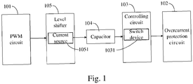
- Fig. 1 is a block diagram of a controlling circuit according to a preferred embodiment of the present disclosure.
- the current easily rises when the LCD panel is turned on or off, which may cause overcurrent protection and thereby cause the panel to fail to be turned on and off normally.
- the problem of the related art can be well dealt with by the embodiment of the present disclosure.
- the controlling circuit capable of controlling boot-up/shutdown of the LCD panel proposed by the present disclosure includes a pulse width modulation (PWM) circuit 101, a level shifter 105, and a capacitor 104.
- the PWM circuit 101 is configured to generate a pulse signal which can change pulses.
- the level shifter 105 is configured to shift an input current from at a high voltage level to at a low voltage level and vice versa.
- a current source 1051 is arranged in the level shifter 105.
- the current source 1051 is configured to supply a constant current.
- the capacitor 104 is arranged outside the level shifter 105. An input terminal of the capacitor 104 is connected to an output terminal of the current source 1051.
- the current source 1051 charges the capacitor 104.
- An output terminal of the capacitor 104 outputs a controlling signal.
- the controlling circuit further includes an overcurrent protection circuit 102.
- the overcurrent protection circuit 102 is connected to the level shifter 105.
- a controlling circuit 103 is arranged between the level shifter 105 and the overcurrent protection circuit 102.
- the controlling circuit 103 includes one or more a switch device 1031. An input of the switch device 1031 is connected to an output terminal of the capacitor 104. An output terminal of the switch device 1031 is connected to a controlling terminal of the overcurrent protection circuit 102.
- An output terminal of the overcurrent protection circuit 102 is connected to a gate driver on array (GOA) circuit.
- the GOA circuit is configured to drive the display of the pixels.
- the overcurrent protection circuit 102 lowers the current and then outputs the current while a large amount of current flows through instantaneously, which prevents the GOA circuit from being damaged by an overloaded current.
- the controlling circuit 103 is configured to enable or cancel a function of overcurrent protection of the overcurrent protection circuit 102 within the designated time, thereby selectively controlling the volume of current which flows to the GOA circuit.
- the PWM circuit 101 When the LCD panel is turned on, the current flows through the PWM circuit 101, and the PWM circuit 101 outputs the pulse signal.
- the output pulse signal enters the level shifter 105.
- the current source 1051 is arranged in the level shifter 105 and outputs the constant current to charge the capacitor 104.
- the charging duration of the capacitor 104 is controlled by the pulse width of the pulse signal to control the voltage imposed on the capacitor 104.
- the switch device 1031 outputs a corresponding signal to the overcurrent protection circuit 102 based on the voltage imposed on the capacitor 104.
- the overcurrent protection circuit 102 decides to enable the function of overcurrent protection according to the input signal.
- the current flowing through the overcurrent protection circuit 102 is not pulled down by the overcurrent protection circuit 102 at the moment of boot-up to turn on the GOA circuit normally.
- Another example is that the current flowing through the overcurrent protection circuit 102 is pulled down by the overcurrent protection circuit 102 after the panel has been turned on for a period of time. The current flows into the GOA circuit to drive the LCD panel.
- the switch device 1031 is a comparator.
- a non-inverting terminal of the comparator is connected to an output terminal of the capacitor 104.
- An inverting terminal of the comparator receives reference voltage.
- An output terminal of the comparator is connected to the overcurrent protection circuit 102.
- the capacitor 104 supplies the controlling voltage to the comparator. After the comparator compares the controlling voltage with the reference voltage, a high voltage level or a low voltage level is output to control the overcurrent protection circuit. For example, when the controlling voltage is less than the reference voltage, the comparator outputs the low voltage level, and the overcurrent protection circuit 102 is turned off; when the controlling voltage is greater than the reference voltage, the comparator outputs the low voltage level, and the overcurrent protection circuit 102 is turned on.
- the switch device 1031 may be a triode.
- a controlling terminal of the triode is connected to the output terminal of the capacitor 104.
- An input terminal of the triode is connected to an enabling power supply.
- An output terminal of the triode is connected to the overcurrent protection circuit 102.
- the capacitor 104 supplies the controlling voltage to the controlling terminal of the triode.
- the enabling power supply supplies enabling voltage to the overcurrent protection circuit 102. After the controlling voltage reaches the conducted amount of voltage of the triode, the enabling voltage is output to the overcurrent protection circuit 102 through the input terminal of the triode and the output terminal of the triode subsequently, thereby enabling the overcurrent protection circuit 102.
- the capacitor 104 supplies the controlling voltage to the controlling terminal of the triode.
- MOS metal-oxide-semiconductor
- the capacitor 104 supplies a high-voltage-level controlling voltage to the controlling terminal of the triode.
- the MOS transistor is turned on.
- the overcurrent protection circuit 102 is enabled once the enabling voltage is imposed on the overcurrent protection circuit 102.
- the capacitor 104 supplies a low-voltage-level controlling voltage to the controlling terminal of the triode within the designated time of boot-up operation.
- the MOS transistor is cut off.
- the overcurrent protection circuit 102 is closed once the enabling voltage is not imposed on the overcurrent protection circuit 102.
- the present disclosure also provides a liquid crystal display (LCD) panel having an LCD body and a controlling circuit.
- the controlling circuit includes a pulse width modulation (PWM) circuit, a level shifter connected to an output terminal of the PWM circuit and having a current source arranged in the level shifter, a capacitor comprising an input terminal connected to an output terminal of the current source that supplies a constant current to the capacitor, an overcurrent protection circuit connected to an output terminal of the level shifter, and a controlling circuit configured to enable or disable a function of overcurrent protection of the overcurrent protection circuit within designated time.
- the controlling circuit includes a switch device. An input of the switch device is connected to an output terminal of the capacitor. An output terminal of the switch device is connected to a controlling terminal of the overcurrent protection circuit.
- the working principle of the LCD panel proposed by the present embodiment is consistent with the controlling circuit of the LCD panel introduced in the above-mentioned embodiment.
- the details of the working principle of the controlling circuit of the LCD panel have been discussed above, which can be referred if needed.
Landscapes
- Physics & Mathematics (AREA)
- Engineering & Computer Science (AREA)
- Chemical & Material Sciences (AREA)
- Crystallography & Structural Chemistry (AREA)
- General Physics & Mathematics (AREA)
- Computer Hardware Design (AREA)
- Theoretical Computer Science (AREA)
- Nonlinear Science (AREA)
- Mathematical Physics (AREA)
- Optics & Photonics (AREA)
- Power Engineering (AREA)
- Liquid Crystal Display Device Control (AREA)
- Control Of Indicators Other Than Cathode Ray Tubes (AREA)
- Emergency Protection Circuit Devices (AREA)
- Liquid Crystal (AREA)
- Dc-Dc Converters (AREA)
Abstract
Description
- The present disclosure relates to the field of a liquid crystal display (LCD) technique, and more particularly, to a controlling circuit and an LCD panel with the controlling circuit.
- With regard to driving a thin film transistor liquid crystal display (TFT LCD) panel of the related art, power supplies are used more and more diversely such as level shifter and pulse width modulation integrated circuit (PWM IC). A large amount of current is often produced when boot-up and shutdown operates due to causes of the difference aging of the panel of the related art, outputting capacitors, and boot-up and shutdown time interval. Practically, such a large amount of current seldom occurs in a normal condition while happening on the boot-up operation. However, overcurrent protection is triggered when boot-up starts, which causes abnormal boot-up and shutdown and unsuccessful operation.
- The problem of the LCD panel of the related art is that the current easily increases when the LCD panel is turned on or off, which may cause overcurrent protection and thereby cause the panel to be turned on and off normally.
- An object of the present disclosure is to propose a controlling circuit which can prevent enabling overcurrent protection for a panel on boot-up and shutdown conditions, thereby realizing normal boot-up and shutdown of the panel. The problem of the related art that overcurrent protection easily occurs when a large amount of current is produced on boot-up and shutdown conditions, causing the panel to fail to be turned on and off normally.
- The present disclosure provides:
- a controlling circuit includes:
- a pulse width modulation (PWM) circuit;
- a level shifter connected to an output terminal of the PWM circuit and having a current source arranged in the level shifter;
- a capacitor comprising an input terminal connected to an output terminal of the current source that supplies a constant current to the capacitor;
- an overcurrent protection circuit connected to an output terminal of the level shifter; and
- a controlling circuit configured to enable or disable a function of overcurrent protection of the overcurrent protection circuit within designated time. The controlling circuit includes a switch device. An input of the switch device is connected to an output terminal of the capacitor. An output terminal of the switch device is connected to a controlling terminal of the overcurrent protection circuit. The designated time is predetermined time which from the start of boot-up operation or shutdown operation correspond to.
- According to a preferred embodiment of the present disclosure, the switch device is a comparator.
- The switch device comprises a non-inverting terminal connected to the output terminal of the capacitor, an inverting terminal receiving reference voltage, and an output terminal connected to the overcurrent protection circuit.
- According to a preferred embodiment of the present disclosure, the switch device is a triode.
- The switch device comprises a controlling terminal connected to the output terminal of the capacitor, an input terminal connected to an enabling power supply, and an output terminal connected to the overcurrent protection circuit.
- According to a preferred embodiment of the present disclosure, an output terminal of the overcurrent protection circuit is connected to a gate driver on array (GOA) circuit.
- According to a second aspect of the present disclosure, a controlling circuit includes:
- a pulse width modulation (PWM) circuit;
- a level shifter connected to an output terminal of the PWM circuit and having a current source arranged in the level shifter;
- a capacitor comprising an input terminal connected to an output terminal of the current source that supplies a constant current to the capacitor;
- an overcurrent protection circuit connected to an output terminal of the level shifter; and
- a controlling circuit configured to enable or disable a function of overcurrent protection of the overcurrent protection circuit within designated time. The controlling circuit includes a switch device. An input of the switch device is connected to an output terminal of the capacitor. An output terminal of the switch device is connected to a controlling terminal of the overcurrent protection circuit.
- According to a preferred embodiment of the present disclosure, the switch device is a comparator.
- The switch device comprises a non-inverting terminal connected to the output terminal of the capacitor, an inverting terminal receiving reference voltage, and an output terminal connected to the overcurrent protection circuit.
- According to a preferred embodiment of the present disclosure, the switch device is a triode.
- The switch device comprises a controlling terminal connected to the output terminal of the capacitor, an input terminal connected to an enabling power supply, and an output terminal connected to the overcurrent protection circuit.
- According to a preferred embodiment of the present disclosure, an output terminal of the overcurrent protection circuit is connected to a gate driver on array (GOA) circuit.
- According to a third aspect of the present disclosure, a liquid crystal display (LCD) panel includes an LCD body and a controlling circuit. The controlling circuit includes:
- a pulse width modulation (PWM) circuit;
- a level shifter connected to an output terminal of the PWM circuit and having a current source arranged in the level shifter;
- a capacitor comprising an input terminal connected to an output terminal of the current source that supplies a constant current to the capacitor;
- an overcurrent protection circuit connected to an output terminal of the level shifter; and
- a controlling circuit configured to enable or disable a function of overcurrent protection of the overcurrent protection circuit within designated time. The controlling circuit includes a switch device. An input of the switch device is connected to an output terminal of the capacitor. An output terminal of the switch device is connected to a controlling terminal of the overcurrent protection circuit.
- According to a preferred embodiment of the present disclosure, the switch device is a comparator.
- The switch device comprises a non-inverting terminal connected to the output terminal of the capacitor, an inverting terminal receiving reference voltage, and an output terminal connected to the overcurrent protection circuit.
- According to a preferred embodiment of the present disclosure, the switch device is a triode.
- The switch device comprises a controlling terminal connected to the output terminal of the capacitor, an input terminal connected to an enabling power supply, and an output terminal connected to the overcurrent protection circuit.
- According to a preferred embodiment of the present disclosure, the designated time is predetermined time which from the start of boot-up operation or shutdown operation correspond to.
- According to a preferred embodiment of the present disclosure, an output terminal of the overcurrent protection circuit is connected to a gate driver on array (GOA) circuit.
- Compared with the controlling circuit of the related art, a controlling circuit is arranged in the controlling circuit proposed by the present disclosure. The controlling circuit controls an overcurrent protection circuit to turn on properly, which realizes normal boot-up and shutdown of the panel. As for the problem that the current easily rises when the LCD panel of the related art is turned on or off, which may cause overcurrent protection and thereby cause the panel to fail to be turned on and off normally. The embodiment of the present disclosure can solve the problem successfully.
- The accompanying drawings are included to provide a further understanding of the invention, and are incorporated in and constitute a part of this specification. The drawings illustrate embodiments of the invention and, together with the description, serve to explain the principles of the invention.
-
Fig. 1 is a block diagram of a controlling circuit according to a preferred embodiment of the present disclosure. - Spatially relative terms, such as "beneath", "below", "lower", "above", "upper" and the like, may be used herein for ease of description to describe one element or feature's relationship to another element(s) or feature(s) as illustrated in the figures. It will be understood that the spatially relative terms are intended to encompass different orientations of the device in use or operation in addition to the orientation depicted in the figures.
- As for the LCD panel of the related art, the current easily rises when the LCD panel is turned on or off, which may cause overcurrent protection and thereby cause the panel to fail to be turned on and off normally. The problem of the related art can be well dealt with by the embodiment of the present disclosure.
- As
Fig. 1 illustrates, the controlling circuit capable of controlling boot-up/shutdown of the LCD panel proposed by the present disclosure includes a pulse width modulation (PWM)circuit 101, alevel shifter 105, and acapacitor 104. ThePWM circuit 101 is configured to generate a pulse signal which can change pulses. Thelevel shifter 105 is configured to shift an input current from at a high voltage level to at a low voltage level and vice versa. Acurrent source 1051 is arranged in thelevel shifter 105. Thecurrent source 1051 is configured to supply a constant current. Thecapacitor 104 is arranged outside thelevel shifter 105. An input terminal of thecapacitor 104 is connected to an output terminal of thecurrent source 1051. Thecurrent source 1051 charges thecapacitor 104. An output terminal of thecapacitor 104 outputs a controlling signal. - The controlling circuit further includes an
overcurrent protection circuit 102. Theovercurrent protection circuit 102 is connected to thelevel shifter 105. Acontrolling circuit 103 is arranged between thelevel shifter 105 and theovercurrent protection circuit 102. Thecontrolling circuit 103 includes one or more aswitch device 1031. An input of theswitch device 1031 is connected to an output terminal of thecapacitor 104. An output terminal of theswitch device 1031 is connected to a controlling terminal of theovercurrent protection circuit 102. - An output terminal of the
overcurrent protection circuit 102 is connected to a gate driver on array (GOA) circuit. The GOA circuit is configured to drive the display of the pixels. Theovercurrent protection circuit 102 lowers the current and then outputs the current while a large amount of current flows through instantaneously, which prevents the GOA circuit from being damaged by an overloaded current. - The
controlling circuit 103 is configured to enable or cancel a function of overcurrent protection of theovercurrent protection circuit 102 within the designated time, thereby selectively controlling the volume of current which flows to the GOA circuit. - When the LCD panel is turned on, the current flows through the
PWM circuit 101, and thePWM circuit 101 outputs the pulse signal. The output pulse signal enters thelevel shifter 105. Thecurrent source 1051 is arranged in thelevel shifter 105 and outputs the constant current to charge thecapacitor 104. The charging duration of thecapacitor 104 is controlled by the pulse width of the pulse signal to control the voltage imposed on thecapacitor 104. Theswitch device 1031 outputs a corresponding signal to theovercurrent protection circuit 102 based on the voltage imposed on thecapacitor 104. Theovercurrent protection circuit 102 decides to enable the function of overcurrent protection according to the input signal. For example, the current flowing through theovercurrent protection circuit 102 is not pulled down by theovercurrent protection circuit 102 at the moment of boot-up to turn on the GOA circuit normally. Another example is that the current flowing through theovercurrent protection circuit 102 is pulled down by theovercurrent protection circuit 102 after the panel has been turned on for a period of time. The current flows into the GOA circuit to drive the LCD panel. - The
switch device 1031 is a comparator. A non-inverting terminal of the comparator is connected to an output terminal of thecapacitor 104. An inverting terminal of the comparator receives reference voltage. An output terminal of the comparator is connected to theovercurrent protection circuit 102. - When the controlling circuit works, the
capacitor 104 supplies the controlling voltage to the comparator. After the comparator compares the controlling voltage with the reference voltage, a high voltage level or a low voltage level is output to control the overcurrent protection circuit. For example, when the controlling voltage is less than the reference voltage, the comparator outputs the low voltage level, and theovercurrent protection circuit 102 is turned off; when the controlling voltage is greater than the reference voltage, the comparator outputs the low voltage level, and theovercurrent protection circuit 102 is turned on. - The
switch device 1031 may be a triode. A controlling terminal of the triode is connected to the output terminal of thecapacitor 104. An input terminal of the triode is connected to an enabling power supply. An output terminal of the triode is connected to theovercurrent protection circuit 102. Thecapacitor 104 supplies the controlling voltage to the controlling terminal of the triode. The enabling power supply supplies enabling voltage to theovercurrent protection circuit 102. After the controlling voltage reaches the conducted amount of voltage of the triode, the enabling voltage is output to theovercurrent protection circuit 102 through the input terminal of the triode and the output terminal of the triode subsequently, thereby enabling theovercurrent protection circuit 102. - When the controlling circuit operates, the
capacitor 104 supplies the controlling voltage to the controlling terminal of the triode. Take an N-type metal-oxide-semiconductor (MOS) transistor for example. Thecapacitor 104 supplies a high-voltage-level controlling voltage to the controlling terminal of the triode. The MOS transistor is turned on. Theovercurrent protection circuit 102 is enabled once the enabling voltage is imposed on theovercurrent protection circuit 102. For example, thecapacitor 104 supplies a low-voltage-level controlling voltage to the controlling terminal of the triode within the designated time of boot-up operation. The MOS transistor is cut off. Theovercurrent protection circuit 102 is closed once the enabling voltage is not imposed on theovercurrent protection circuit 102. - The present disclosure also provides a liquid crystal display (LCD) panel having an LCD body and a controlling circuit. The controlling circuit includes a pulse width modulation (PWM) circuit, a level shifter connected to an output terminal of the PWM circuit and having a current source arranged in the level shifter, a capacitor comprising an input terminal connected to an output terminal of the current source that supplies a constant current to the capacitor, an overcurrent protection circuit connected to an output terminal of the level shifter, and a controlling circuit configured to enable or disable a function of overcurrent protection of the overcurrent protection circuit within designated time. The controlling circuit includes a switch device. An input of the switch device is connected to an output terminal of the capacitor. An output terminal of the switch device is connected to a controlling terminal of the overcurrent protection circuit.
- The working principle of the LCD panel proposed by the present embodiment is consistent with the controlling circuit of the LCD panel introduced in the above-mentioned embodiment. The details of the working principle of the controlling circuit of the LCD panel have been discussed above, which can be referred if needed.
- The present disclosure is described in detail in accordance with the above contents with the specific preferred examples. However, this present disclosure is not limited to the specific examples. For the ordinary technical personnel of the technical field of the present disclosure, on the premise of keeping the conception of the present disclosure, the technical personnel can also make simple deductions or replacements, and all of which should be considered to belong to the protection scope of the present disclosure.
Claims (13)
- A controlling circuit, characterized in that the controlling circuit comprises:a pulse width modulation (PWM) circuit;a level shifter, connected to an output terminal of the PWM circuit; a current source arranged in the level shifter;a capacitor, comprising an input terminal connected to an output terminal of the current source that supplies a constant current to the capacitor;an overcurrent protection circuit, connected to an output terminal of the level shifter; anda controlling circuit, configured to enable or disable a function of overcurrent protection of the overcurrent protection circuit within designated time; the controlling circuit comprising a switch device; an input of the switch device connected to an output terminal of the capacitor; an output terminal of the switch device connected to a controlling terminal of the overcurrent protection circuit; the designated time is predetermined time which from the start of boot-up operation or shutdown operation correspond to.
- The controlling circuit of claim 1, characterized in that the switch device is a comparator that comprises a non-inverting terminal connected to the output terminal of the capacitor, an inverting terminal receiving reference voltage, and an output terminal connected to the overcurrent protection circuit.
- The controlling circuit of claim 1, characterized in that the switch device is a triode that comprises a controlling terminal connected to the output terminal of the capacitor, an input terminal connected to an enabling power supply, and an output terminal connected to the overcurrent protection circuit.
- The controlling circuit of claim 1, characterized in that an output terminal of the overcurrent protection circuit is connected to a gate driver on array (GOA) circuit.
- A controlling circuit, characterized in that the controlling circuit comprises:a pulse width modulation (PWM) circuit;a level shifter, connected to an output terminal of the PWM circuit; a current source arranged in the level shifter;a capacitor, comprising an input terminal connected to an output terminal of the current source that supplies a constant current to the capacitor;an overcurrent protection circuit, connected to an output terminal of the level shifter; anda controlling circuit, configured to enable or disable a function of overcurrent protection of the overcurrent protection circuit within designated time; the controlling circuit comprising a switch device; an input of the switch device connected to an output terminal of the capacitor; an output terminal of the switch device connected to a controlling terminal of the overcurrent protection circuit.
- The controlling circuit of claim 5, characterized in that the switch device is a comparator that comprises a non-inverting terminal connected to the output terminal of the capacitor, an inverting terminal receiving reference voltage, and an output terminal connected to the overcurrent protection circuit.
- The controlling circuit of claim 5, characterized in that the switch device is a triode that comprises a controlling terminal connected to the output terminal of the capacitor, an input terminal connected to an enabling power supply, and an output terminal connected to the overcurrent protection circuit.
- The controlling circuit of claim 5, characterized in that an output terminal of the overcurrent protection circuit is connected to a gate driver on array (GOA) circuit.
- A liquid crystal display (LCD) panel comprising an LCD body and a controlling circuit, characterized in that the controlling circuit comprises:a pulse width modulation (PWM) circuit;a level shifter, connected to an output terminal of the PWM circuit; a current source arranged in the level shifter;a capacitor, comprising an input terminal connected to an output terminal of the current source that supplies a constant current to the capacitor;an overcurrent protection circuit, connected to an output terminal of the level shifter; anda controlling circuit, configured to enable or disable a function of overcurrent protection of the overcurrent protection circuit within designated time; the controlling circuit comprising a switch device; an input of the switch device connected to an output terminal of the capacitor; an output terminal of the switch device connected to a controlling terminal of the overcurrent protection circuit.
- The LCD panel of claim 9, characterized in that the switch device is a comparator that comprises a non-inverting terminal connected to the output terminal of the capacitor, an inverting terminal receiving reference voltage, and an output terminal connected to the overcurrent protection circuit.
- The LCD panel of claim 9, characterized in that the switch device is a triode that comprises a controlling terminal connected to the output terminal of the capacitor, an input terminal connected to an enabling power supply, and an output terminal connected to the overcurrent protection circuit.
- The LCD panel of claim 9, characterized in that the designated time is predetermined time which from the start of boot-up operation or shutdown operation correspond to.
- The LCD panel of claim 9, characterized in that an output terminal of the overcurrent protection circuit is connected to a gate driver on array (GOA) circuit.
Applications Claiming Priority (2)
| Application Number | Priority Date | Filing Date | Title |
|---|---|---|---|
| CN201710918653.1A CN107527602B (en) | 2017-09-30 | 2017-09-30 | Liquid crystal display panel and switching on and shutting down control circuit |
| PCT/CN2017/109526 WO2019061682A1 (en) | 2017-09-30 | 2017-11-06 | Liquid crystal display panel and startup/shutdown control circuit |
Publications (2)
| Publication Number | Publication Date |
|---|---|
| EP3691126A1 true EP3691126A1 (en) | 2020-08-05 |
| EP3691126A4 EP3691126A4 (en) | 2021-08-18 |
Family
ID=60684261
Family Applications (1)
| Application Number | Title | Priority Date | Filing Date |
|---|---|---|---|
| EP17926450.2A Withdrawn EP3691126A4 (en) | 2017-09-30 | 2017-11-06 | LIQUID CRYSTAL DISPLAY AND START / STOP CONTROL CIRCUIT |
Country Status (6)
| Country | Link |
|---|---|
| US (1) | US10698238B2 (en) |
| EP (1) | EP3691126A4 (en) |
| JP (1) | JP7150019B2 (en) |
| KR (1) | KR20200055125A (en) |
| CN (1) | CN107527602B (en) |
| WO (1) | WO2019061682A1 (en) |
Families Citing this family (5)
| Publication number | Priority date | Publication date | Assignee | Title |
|---|---|---|---|---|
| CN108831361B (en) * | 2018-06-25 | 2021-06-25 | 南京熊猫电子制造有限公司 | LED backlight driving circuit |
| CN109637412B (en) * | 2018-12-25 | 2020-10-30 | 惠科股份有限公司 | Overcurrent protection method of display panel and display device |
| CN112992038B (en) * | 2021-03-09 | 2023-03-17 | 深圳市华星光电半导体显示技术有限公司 | Display panel and display device |
| JP2025033476A (en) * | 2023-08-29 | 2025-03-13 | シャープディスプレイテクノロジー株式会社 | Display device |
| WO2025043653A1 (en) * | 2023-08-31 | 2025-03-06 | 京东方科技集团股份有限公司 | Level conversion assembly, overcurrent protection method, and display device |
Family Cites Families (25)
| Publication number | Priority date | Publication date | Assignee | Title |
|---|---|---|---|---|
| JPS6143729U (en) * | 1984-08-24 | 1986-03-22 | オムロン株式会社 | Motor protection circuit |
| JPH02193520A (en) * | 1989-01-20 | 1990-07-31 | Fujitsu General Ltd | Power source interrupting method with excess current detector |
| JPH0385014A (en) * | 1989-08-29 | 1991-04-10 | Sharp Corp | Pwm/dc voltage conversion circuit |
| JPH0583842A (en) * | 1991-09-18 | 1993-04-02 | Mitsubishi Electric Corp | Overcurrent protection relay |
| JP3305257B2 (en) * | 1998-05-06 | 2002-07-22 | セイコーインスツルメンツ株式会社 | Charge / discharge control circuit, rechargeable power supply device and control method therefor |
| JP5114818B2 (en) * | 2001-08-13 | 2013-01-09 | ヤマハ株式会社 | Current detection method, current detection circuit and overcurrent protection circuit |
| KR100927013B1 (en) | 2002-11-22 | 2009-11-16 | 엘지디스플레이 주식회사 | LCD and its driving method |
| US8405321B2 (en) * | 2007-07-26 | 2013-03-26 | Rohm Co., Ltd. | Drive unit, smoothing circuit, DC/DC converter |
| JP2009165285A (en) | 2008-01-08 | 2009-07-23 | Panasonic Corp | Semiconductor device |
| CN201868077U (en) * | 2010-02-04 | 2011-06-15 | 福建省冠林科技有限公司 | Stimulating TFT (Thin Film Transistor) display screen driving circuit with display screen-opening delay function |
| JP2011244677A (en) | 2010-04-23 | 2011-12-01 | Rohm Co Ltd | Control circuit for switching power supply, and switching power supply, light-emitting device and electronic apparatus with the same |
| JP5470150B2 (en) | 2010-04-23 | 2014-04-16 | ローム株式会社 | Switching power supply control circuit, control method, and light emitting device and electronic apparatus using them |
| JP5492728B2 (en) | 2010-09-28 | 2014-05-14 | 株式会社ジャパンディスプレイ | Display device |
| WO2013005529A1 (en) * | 2011-07-01 | 2013-01-10 | ローム株式会社 | Overvoltage protection circuit, power supply apparatus, liquid crystal display apparatus, electronic apparatus, and television set |
| JP6076630B2 (en) * | 2012-07-11 | 2017-02-08 | ローム株式会社 | Driver circuit |
| CN203135828U (en) * | 2013-03-04 | 2013-08-14 | 力博特公司 | Power source powering on/off circuit |
| CN203457042U (en) * | 2013-09-04 | 2014-02-26 | 陕西中科天地航空模块有限公司 | Switching power supply of pulse switching machine |
| CN103869722B (en) * | 2014-04-08 | 2017-01-04 | 广东宝莱特医用科技股份有限公司 | A kind of controlling hard switch machine system |
| WO2017187785A1 (en) * | 2016-04-28 | 2017-11-02 | ローム株式会社 | Overcurrent protection circuit |
| JP6712199B2 (en) * | 2016-08-10 | 2020-06-17 | ローム株式会社 | Overcurrent protection circuit |
| US10756720B2 (en) * | 2016-10-17 | 2020-08-25 | Infineon Technologies Ag | Driver circuit for electronic switch |
| CN106683621B (en) * | 2016-12-30 | 2024-03-29 | 厦门厦华科技有限公司 | LED backlight driving circuit and method for realizing soft start |
| CN106648020A (en) * | 2017-01-05 | 2017-05-10 | 郑州云海信息技术有限公司 | Method and apparatus for preventing over-current protection malfunction |
| CN107040738B (en) * | 2017-04-14 | 2020-03-17 | 四川长虹电器股份有限公司 | Circuit for eliminating voltage and current exceeding standard when signal functional module starts power-on |
| CN106991988B (en) * | 2017-05-17 | 2019-07-02 | 深圳市华星光电技术有限公司 | The over-current protection system and method for GOA circuit |
-
2017
- 2017-09-30 CN CN201710918653.1A patent/CN107527602B/en not_active Expired - Fee Related
- 2017-11-06 US US15/574,969 patent/US10698238B2/en not_active Expired - Fee Related
- 2017-11-06 JP JP2020530716A patent/JP7150019B2/en active Active
- 2017-11-06 WO PCT/CN2017/109526 patent/WO2019061682A1/en not_active Ceased
- 2017-11-06 EP EP17926450.2A patent/EP3691126A4/en not_active Withdrawn
- 2017-11-06 KR KR1020207012481A patent/KR20200055125A/en not_active Ceased
Also Published As
| Publication number | Publication date |
|---|---|
| JP7150019B2 (en) | 2022-10-07 |
| CN107527602B (en) | 2019-07-16 |
| EP3691126A4 (en) | 2021-08-18 |
| US10698238B2 (en) | 2020-06-30 |
| WO2019061682A1 (en) | 2019-04-04 |
| JP2020532275A (en) | 2020-11-05 |
| KR20200055125A (en) | 2020-05-20 |
| CN107527602A (en) | 2017-12-29 |
| US20190101777A1 (en) | 2019-04-04 |
Similar Documents
| Publication | Publication Date | Title |
|---|---|---|
| US10698238B2 (en) | Liquid crystal display panel and controlling circuit | |
| EP3751552B1 (en) | Residual image elimination unit, control method therefor and liquid crystal display device | |
| US8976164B2 (en) | Circuit for eliminating shutdown afterimages of a display device | |
| US9799269B2 (en) | Pixel circuit, display panel and driving method thereof | |
| CN207781164U (en) | A kind of ghost eliminates circuit, display device and its driving circuit | |
| EP3657487A1 (en) | Display driving chip and liquid crystal display device | |
| US10510313B2 (en) | Driving circuit outputting a chamfered wave scanning signal, driving method and display apparatus | |
| US10008173B2 (en) | Liquid crystal display device with a discharge control circuit | |
| US20180301200A1 (en) | Control circuit for controlling a noise reduction thin film transistor in a shift register unit and method of reducing noise | |
| US20150280700A1 (en) | Apparatus for supplying gate driving voltages, method therefor and display apparatus | |
| EP3553768B1 (en) | Method and apparatus for controlling power source of display screen, and storage medium and electronic device | |
| KR101978618B1 (en) | LCD screen signal control circuit, display panel and display device | |
| US9025349B2 (en) | Power system and starting method thereof with small changed or unchanged PWM output | |
| KR20230054317A (en) | Current control circuit, display panel driving device and display device | |
| US9734784B2 (en) | Voltage output device, gate driving circuit and display apparatus | |
| US11074878B2 (en) | Liquid crystal display | |
| US9703304B2 (en) | Voltage booster circuit, semiconductor device, and voltage booster circuit control method | |
| CN101556778A (en) | Method for optimizing display effect at power off and circuit thereof | |
| US20210118398A1 (en) | Display device, drive voltage setting method, and computer program | |
| JP2007233202A (en) | Liquid crystal display | |
| WO2012001785A1 (en) | Display device and display device control method | |
| JP3799869B2 (en) | Semiconductor device equipped with power supply circuit, and liquid crystal device and electronic device using the same | |
| KR20090073646A (en) | LCD and its driving method | |
| KR102551574B1 (en) | Power supply device and display device | |
| KR20210060912A (en) | Display device and driving method thereof |
Legal Events
| Date | Code | Title | Description |
|---|---|---|---|
| STAA | Information on the status of an ep patent application or granted ep patent |
Free format text: STATUS: THE INTERNATIONAL PUBLICATION HAS BEEN MADE |
|
| PUAI | Public reference made under article 153(3) epc to a published international application that has entered the european phase |
Free format text: ORIGINAL CODE: 0009012 |
|
| STAA | Information on the status of an ep patent application or granted ep patent |
Free format text: STATUS: REQUEST FOR EXAMINATION WAS MADE |
|
| 17P | Request for examination filed |
Effective date: 20200427 |
|
| AK | Designated contracting states |
Kind code of ref document: A1 Designated state(s): AL AT BE BG CH CY CZ DE DK EE ES FI FR GB GR HR HU IE IS IT LI LT LU LV MC MK MT NL NO PL PT RO RS SE SI SK SM TR |
|
| AX | Request for extension of the european patent |
Extension state: BA ME |
|
| DAV | Request for validation of the european patent (deleted) | ||
| DAX | Request for extension of the european patent (deleted) | ||
| A4 | Supplementary search report drawn up and despatched |
Effective date: 20210720 |
|
| RIC1 | Information provided on ipc code assigned before grant |
Ipc: H03K 17/08 20060101AFI20210714BHEP Ipc: G09G 3/36 20060101ALI20210714BHEP |
|
| GRAP | Despatch of communication of intention to grant a patent |
Free format text: ORIGINAL CODE: EPIDOSNIGR1 |
|
| STAA | Information on the status of an ep patent application or granted ep patent |
Free format text: STATUS: GRANT OF PATENT IS INTENDED |
|
| INTG | Intention to grant announced |
Effective date: 20221108 |
|
| STAA | Information on the status of an ep patent application or granted ep patent |
Free format text: STATUS: THE APPLICATION IS DEEMED TO BE WITHDRAWN |
|
| 18D | Application deemed to be withdrawn |
Effective date: 20230321 |