EP3686905A1 - Electrode substrate for transparent light-emitting device display, and manufacturing method therefor - Google Patents
Electrode substrate for transparent light-emitting device display, and manufacturing method therefor Download PDFInfo
- Publication number
- EP3686905A1 EP3686905A1 EP18857644.1A EP18857644A EP3686905A1 EP 3686905 A1 EP3686905 A1 EP 3686905A1 EP 18857644 A EP18857644 A EP 18857644A EP 3686905 A1 EP3686905 A1 EP 3686905A1
- Authority
- EP
- European Patent Office
- Prior art keywords
- copper foil
- pattern
- transparent
- resin composition
- photosensitive resin
- Prior art date
- Legal status (The legal status is an assumption and is not a legal conclusion. Google has not performed a legal analysis and makes no representation as to the accuracy of the status listed.)
- Granted
Links
Images



Classifications
-
- H—ELECTRICITY
- H10—SEMICONDUCTOR DEVICES; ELECTRIC SOLID-STATE DEVICES NOT OTHERWISE PROVIDED FOR
- H10H—INORGANIC LIGHT-EMITTING SEMICONDUCTOR DEVICES HAVING POTENTIAL BARRIERS
- H10H20/00—Individual inorganic light-emitting semiconductor devices having potential barriers, e.g. light-emitting diodes [LED]
- H10H20/80—Constructional details
- H10H20/85—Packages
- H10H20/857—Interconnections, e.g. lead-frames, bond wires or solder balls
-
- H—ELECTRICITY
- H01—ELECTRIC ELEMENTS
- H01B—CABLES; CONDUCTORS; INSULATORS; SELECTION OF MATERIALS FOR THEIR CONDUCTIVE, INSULATING OR DIELECTRIC PROPERTIES
- H01B13/00—Apparatus or processes specially adapted for manufacturing conductors or cables
- H01B13/0026—Apparatus for manufacturing conducting or semi-conducting layers, e.g. deposition of metal
-
- H—ELECTRICITY
- H05—ELECTRIC TECHNIQUES NOT OTHERWISE PROVIDED FOR
- H05K—PRINTED CIRCUITS; CASINGS OR CONSTRUCTIONAL DETAILS OF ELECTRIC APPARATUS; MANUFACTURE OF ASSEMBLAGES OF ELECTRICAL COMPONENTS
- H05K3/00—Apparatus or processes for manufacturing printed circuits
- H05K3/0073—Masks not provided for in groups H05K3/02 - H05K3/46, e.g. for photomechanical production of patterned surfaces
- H05K3/0082—Masks not provided for in groups H05K3/02 - H05K3/46, e.g. for photomechanical production of patterned surfaces characterised by the exposure method of radiation-sensitive masks
-
- H—ELECTRICITY
- H05—ELECTRIC TECHNIQUES NOT OTHERWISE PROVIDED FOR
- H05K—PRINTED CIRCUITS; CASINGS OR CONSTRUCTIONAL DETAILS OF ELECTRIC APPARATUS; MANUFACTURE OF ASSEMBLAGES OF ELECTRICAL COMPONENTS
- H05K3/00—Apparatus or processes for manufacturing printed circuits
- H05K3/02—Apparatus or processes for manufacturing printed circuits in which the conductive material is applied to the surface of the insulating support and is thereafter removed from such areas of the surface which are not intended for current conducting or shielding
- H05K3/06—Apparatus or processes for manufacturing printed circuits in which the conductive material is applied to the surface of the insulating support and is thereafter removed from such areas of the surface which are not intended for current conducting or shielding the conductive material being removed chemically or electrolytically, e.g. by photo-etch process
- H05K3/067—Etchants
-
- H—ELECTRICITY
- H05—ELECTRIC TECHNIQUES NOT OTHERWISE PROVIDED FOR
- H05K—PRINTED CIRCUITS; CASINGS OR CONSTRUCTIONAL DETAILS OF ELECTRIC APPARATUS; MANUFACTURE OF ASSEMBLAGES OF ELECTRICAL COMPONENTS
- H05K3/00—Apparatus or processes for manufacturing printed circuits
- H05K3/22—Secondary treatment of printed circuits
- H05K3/28—Applying non-metallic protective coatings
- H05K3/285—Permanent coating compositions
- H05K3/287—Photosensitive compositions
-
- H—ELECTRICITY
- H10—SEMICONDUCTOR DEVICES; ELECTRIC SOLID-STATE DEVICES NOT OTHERWISE PROVIDED FOR
- H10H—INORGANIC LIGHT-EMITTING SEMICONDUCTOR DEVICES HAVING POTENTIAL BARRIERS
- H10H20/00—Individual inorganic light-emitting semiconductor devices having potential barriers, e.g. light-emitting diodes [LED]
- H10H20/80—Constructional details
- H10H20/83—Electrodes
- H10H20/832—Electrodes characterised by their material
- H10H20/833—Transparent materials
-
- H—ELECTRICITY
- H10—SEMICONDUCTOR DEVICES; ELECTRIC SOLID-STATE DEVICES NOT OTHERWISE PROVIDED FOR
- H10H—INORGANIC LIGHT-EMITTING SEMICONDUCTOR DEVICES HAVING POTENTIAL BARRIERS
- H10H29/00—Integrated devices, or assemblies of multiple devices, comprising at least one light-emitting semiconductor element covered by group H10H20/00
- H10H29/10—Integrated devices comprising at least one light-emitting semiconductor component covered by group H10H20/00
- H10H29/14—Integrated devices comprising at least one light-emitting semiconductor component covered by group H10H20/00 comprising multiple light-emitting semiconductor components
- H10H29/142—Two-dimensional arrangements, e.g. asymmetric LED layout
-
- H—ELECTRICITY
- H10—SEMICONDUCTOR DEVICES; ELECTRIC SOLID-STATE DEVICES NOT OTHERWISE PROVIDED FOR
- H10P—GENERIC PROCESSES OR APPARATUS FOR THE MANUFACTURE OR TREATMENT OF DEVICES COVERED BY CLASS H10
- H10P14/00—Formation of materials, e.g. in the shape of layers or pillars
- H10P14/20—Formation of materials, e.g. in the shape of layers or pillars of semiconductor materials
- H10P14/29—Formation of materials, e.g. in the shape of layers or pillars of semiconductor materials characterised by the substrates
-
- H—ELECTRICITY
- H10—SEMICONDUCTOR DEVICES; ELECTRIC SOLID-STATE DEVICES NOT OTHERWISE PROVIDED FOR
- H10P—GENERIC PROCESSES OR APPARATUS FOR THE MANUFACTURE OR TREATMENT OF DEVICES COVERED BY CLASS H10
- H10P95/00—Generic processes or apparatus for manufacture or treatments not covered by the other groups of this subclass
-
- H—ELECTRICITY
- H05—ELECTRIC TECHNIQUES NOT OTHERWISE PROVIDED FOR
- H05K—PRINTED CIRCUITS; CASINGS OR CONSTRUCTIONAL DETAILS OF ELECTRIC APPARATUS; MANUFACTURE OF ASSEMBLAGES OF ELECTRICAL COMPONENTS
- H05K2201/00—Indexing scheme relating to printed circuits covered by H05K1/00
- H05K2201/01—Dielectrics
- H05K2201/0104—Properties and characteristics in general
- H05K2201/0108—Transparent
-
- H—ELECTRICITY
- H05—ELECTRIC TECHNIQUES NOT OTHERWISE PROVIDED FOR
- H05K—PRINTED CIRCUITS; CASINGS OR CONSTRUCTIONAL DETAILS OF ELECTRIC APPARATUS; MANUFACTURE OF ASSEMBLAGES OF ELECTRICAL COMPONENTS
- H05K2201/00—Indexing scheme relating to printed circuits covered by H05K1/00
- H05K2201/01—Dielectrics
- H05K2201/0183—Dielectric layers
- H05K2201/0195—Dielectric or adhesive layers comprising a plurality of layers, e.g. in a multilayer structure
-
- H—ELECTRICITY
- H05—ELECTRIC TECHNIQUES NOT OTHERWISE PROVIDED FOR
- H05K—PRINTED CIRCUITS; CASINGS OR CONSTRUCTIONAL DETAILS OF ELECTRIC APPARATUS; MANUFACTURE OF ASSEMBLAGES OF ELECTRICAL COMPONENTS
- H05K2201/00—Indexing scheme relating to printed circuits covered by H05K1/00
- H05K2201/09—Shape and layout
- H05K2201/09209—Shape and layout details of conductors
- H05K2201/09654—Shape and layout details of conductors covering at least two types of conductors provided for in H05K2201/09218 - H05K2201/095
- H05K2201/09681—Mesh conductors, e.g. as a ground plane
-
- H—ELECTRICITY
- H05—ELECTRIC TECHNIQUES NOT OTHERWISE PROVIDED FOR
- H05K—PRINTED CIRCUITS; CASINGS OR CONSTRUCTIONAL DETAILS OF ELECTRIC APPARATUS; MANUFACTURE OF ASSEMBLAGES OF ELECTRICAL COMPONENTS
- H05K2201/00—Indexing scheme relating to printed circuits covered by H05K1/00
- H05K2201/09—Shape and layout
- H05K2201/09818—Shape or layout details not covered by a single group of H05K2201/09009 - H05K2201/09809
- H05K2201/099—Coating over pads, e.g. solder resist partly over pads
-
- H—ELECTRICITY
- H05—ELECTRIC TECHNIQUES NOT OTHERWISE PROVIDED FOR
- H05K—PRINTED CIRCUITS; CASINGS OR CONSTRUCTIONAL DETAILS OF ELECTRIC APPARATUS; MANUFACTURE OF ASSEMBLAGES OF ELECTRICAL COMPONENTS
- H05K2201/00—Indexing scheme relating to printed circuits covered by H05K1/00
- H05K2201/10—Details of components or other objects attached to or integrated in a printed circuit board
- H05K2201/10007—Types of components
- H05K2201/10106—Light emitting diode [LED]
-
- H—ELECTRICITY
- H05—ELECTRIC TECHNIQUES NOT OTHERWISE PROVIDED FOR
- H05K—PRINTED CIRCUITS; CASINGS OR CONSTRUCTIONAL DETAILS OF ELECTRIC APPARATUS; MANUFACTURE OF ASSEMBLAGES OF ELECTRICAL COMPONENTS
- H05K2201/00—Indexing scheme relating to printed circuits covered by H05K1/00
- H05K2201/10—Details of components or other objects attached to or integrated in a printed circuit board
- H05K2201/10007—Types of components
- H05K2201/10128—Display
-
- H—ELECTRICITY
- H05—ELECTRIC TECHNIQUES NOT OTHERWISE PROVIDED FOR
- H05K—PRINTED CIRCUITS; CASINGS OR CONSTRUCTIONAL DETAILS OF ELECTRIC APPARATUS; MANUFACTURE OF ASSEMBLAGES OF ELECTRICAL COMPONENTS
- H05K2201/00—Indexing scheme relating to printed circuits covered by H05K1/00
- H05K2201/20—Details of printed circuits not provided for in H05K2201/01 - H05K2201/10
- H05K2201/2072—Anchoring, i.e. one structure gripping into another
-
- H—ELECTRICITY
- H05—ELECTRIC TECHNIQUES NOT OTHERWISE PROVIDED FOR
- H05K—PRINTED CIRCUITS; CASINGS OR CONSTRUCTIONAL DETAILS OF ELECTRIC APPARATUS; MANUFACTURE OF ASSEMBLAGES OF ELECTRICAL COMPONENTS
- H05K3/00—Apparatus or processes for manufacturing printed circuits
- H05K3/30—Assembling printed circuits with electric components, e.g. with resistors
- H05K3/32—Assembling printed circuits with electric components, e.g. with resistors electrically connecting electric components or wires to printed circuits
- H05K3/34—Assembling printed circuits with electric components, e.g. with resistors electrically connecting electric components or wires to printed circuits by soldering
- H05K3/3452—Solder masks
-
- H—ELECTRICITY
- H10—SEMICONDUCTOR DEVICES; ELECTRIC SOLID-STATE DEVICES NOT OTHERWISE PROVIDED FOR
- H10H—INORGANIC LIGHT-EMITTING SEMICONDUCTOR DEVICES HAVING POTENTIAL BARRIERS
- H10H20/00—Individual inorganic light-emitting semiconductor devices having potential barriers, e.g. light-emitting diodes [LED]
- H10H20/01—Manufacture or treatment
- H10H20/036—Manufacture or treatment of packages
- H10H20/0364—Manufacture or treatment of packages of interconnections
-
- H—ELECTRICITY
- H10—SEMICONDUCTOR DEVICES; ELECTRIC SOLID-STATE DEVICES NOT OTHERWISE PROVIDED FOR
- H10H—INORGANIC LIGHT-EMITTING SEMICONDUCTOR DEVICES HAVING POTENTIAL BARRIERS
- H10H20/00—Individual inorganic light-emitting semiconductor devices having potential barriers, e.g. light-emitting diodes [LED]
- H10H20/80—Constructional details
- H10H20/81—Bodies
-
- H—ELECTRICITY
- H10—SEMICONDUCTOR DEVICES; ELECTRIC SOLID-STATE DEVICES NOT OTHERWISE PROVIDED FOR
- H10W—GENERIC PACKAGES, INTERCONNECTIONS, CONNECTORS OR OTHER CONSTRUCTIONAL DETAILS OF DEVICES COVERED BY CLASS H10
- H10W90/00—Package configurations
Definitions
- the present application relates to an electrode substrate for a transparent light emitting device display and a method of manufacturing the same.
- ITO indium tin oxide
- reserves of indium, which is a main raw material of the material of the ITO transparent electrode are not largely available globally and indium is produced in some countries, such as China, and production cost of indium is high.
- indium has a disadvantage in that a resistance value is not constantly applied, so that an expressed light beam of an LED is not uniform. Accordingly, the transparent LED utilizing ITO has a limit in being utilized as a transparent electrode material with high performance and low cost.
- the ITO has been most dominantly used as a transparent electrode material, but research and technology development utilizing a new material are continuously conducted due to a limit in economic feasibility, restricted performance, and the like.
- a transparent electrode material attracting attention as a next-generation new material, there are metal mesh, an Ag nanowire, carbon nano tube (CNT), conductive polymer, graphene, and the like.
- the metal mesh is a new material, which occupies 85% of a material replacing the ITO, is low cost and has high conductivity, so that a market of the metal mesh is expanded in an aspect of utilization of the metal mesh.
- the transparent LED display utilizing the metal mesh is easily repaired and maintained, is capable of saving resources, is capable of considerably preventing environmental contamination, and is economical by a decrease in manufacturing cost, compared to an existing ITO transparent display. Further, the transparent LED display utilizing the metal mesh may be expansively applied for various purposes and may be applied to and utilized in various products as a new transparent electrode material.
- the present application is aimed at providing an electrode substrate for a transparent light emitting device display and a method of manufacturing the same.
- An exemplary embodiment of the present application provides a method of manufacturing an electrode substrate for a transparent light emitting device display, comprising: laminating copper foil on a transparent base material; forming a copper foil pattern by etching the copper foil; forming a transparent photosensitive resin composition layer on a front surface of the transparent base material and the copper foil pattern; and exposing at least a part of the copper foil pattern by removing at least a part of the transparent photosensitive resin composition layer provided on the copper foil pattern.
- an electrode substrate for a transparent light emitting device display comprising: a transparent base material; an adhesive layer provided on the transparent base material; a copper foil pattern provided on the adhesive layer; and a transparent photosensitive resin composition layer provided on the adhesive layer and the copper foil pattern, in which the transparent photosensitive resin composition layer is not provided in at least a partial region of the copper foil pattern, and haze of a region, in which the copper foil pattern is not provided, in the electrode substrate for the transparent light emitting device display is 5% or less.
- Still another exemplary embodiment of the present application provides a transparent light emitting device display comprising the electrode substrate for the transparent light emitting device display.
- a metal pattern is formed by using low-price copper foil, so that it is possible to decrease raw material cost when an electrode substrate for a transparent light emitting device display is manufactured.
- the transparent photosensitive resin composition layer is formed on the transparent base material and the copper foil pattern, so that it is possible to prevent an increase in haze of the electrode substrate for the transparent light emitting device display due to roughness of the surface of the copper foil, and a refractive index of the transparent photosensitive resin composition layer is adjusted, so that it is possible to decrease haze of the electrode substrate for the transparent light emitting device display.
- At least a part of the copper foil pattern is exposed by removing at least a part of the transparent photosensitive resin composition layer provided on the copper foil pattern, so that it is possible to form an electrode pad unit pattern, which is connected with an external terminal or in which a light emitting device is mounted.
- transparent is defined to have a transmittance characteristic of about 80% or more in a visible ray region (400 nm to 700 nm).
- a transparent electrode substrate applied to a transparent light emitting diode (LED) display needs to secure a low resistance characteristic of 1 ohm/sq or less, and in order to secure low resistance and high transmittance, a metal layer, such as a Cu layer, of 2 ⁇ m or more is required.
- a sputtering method is used for forming the metal layer, but when the sputtering method is used, there is a problem in that it is difficult to secure attachment force between a transparent base material and the metal layer, and a price of the transparent electrode substrate is sharply increased due to an increase in excessive deposition time.
- the present application is aimed at providing an electrode substrate for a transparent light emitting device display, which uses very low-cost copper foil as a metal layer, and a method of manufacturing the same.
- a method of manufacturing an electrode substrate for a transparent light emitting device display comprises: laminating copper foil on a transparent base material; forming a copper foil pattern by etching the copper foil; forming a transparent photosensitive resin composition layer on entire surfaces of upper portions of the transparent base material and the copper foil pattern; and exposing at least a part of the copper foil pattern by removing at least a part of the transparent photosensitive resin composition layer provided on the copper foil pattern.
- the method of manufacturing the electrode substrate for the transparent light emitting device display according to the exemplary embodiment of the present application comprises laminating copper foil on a transparent base material.
- the transparent base material may be a glass base material or a transparent plastic base material having excellent transparency, surface smoothness, treatment easiness, and waterproofing property, but is not limited thereto, and as long as a transparent base material is generally used in an electronic device, the transparent substrate is not limited.
- the transparent base material may be a base material formed of glass, a urethane resin, a polyimide resin, a polyester resin, a (meth)acrylate-based polymer resin; a polyolefin-based resin, such as polyethylene or polypropylene, and the like.
- a material known in the art may be used as the copper foil, and a thickness of the copper foil may be 2 ⁇ m to 15 ⁇ m, but is not limited thereto.
- an adhesive layer may be used. More particularly, the laminating of the copper foil on the transparent base material may comprise forming an adhesive layer on the transparent base material, and forming a copper foil on the adhesive layer.
- the adhesive layer is positioned between the transparent base material and the copper foil and provides attachment force, and a refractive index of the adhesive layer may be 1.45 to 1.55. More particularly, as the adhesive layer, an acrylic resin, a silicon-based resin, an epoxy-based resin, a polyimide-based resin, and the like having a refractive index of 1.45 to 1.55 are used, and the adhesive layer may be formed in a thickness range of 5 ⁇ m to 30 ⁇ m by a method, such as comma coating and slot die coating, but the thickness of the adhesive layer is not limited thereto.
- the method of manufacturing the electrode substrate for the transparent light emitting device display according to the exemplary embodiment of the present application comprises forming a copper foil pattern by etching the copper foil.
- the method of etching the copper foil may comprise forming a resist pattern on the copper foil and then etching the copper foil, and peeling the resist pattern, but is not limited thereto.
- the copper foil pattern may comprise two or more kinds of copper foil pattern having different line widths. Further, the copper foil pattern may comprise two kinds of copper foil pattern having different line widths, and a line width of one kind of copper foil pattern is 3 ⁇ m to 30 ⁇ m, and a line width of the other kind of copper foil pattern is 50 ⁇ m or more.
- the copper foil pattern having the line width of 3 ⁇ m to 30 ⁇ m may serve as an electrode pattern, and the copper foil pattern having the line width of 50 ⁇ m or more may serve as an electrode pad unit pattern for a connection with an external terminal. That is, the copper foil pattern may comprise an electrode pattern and an electrode pad unit pattern. Further, a light emitting device may be mounted on the electrode pad unit pattern.
- a line width of the electrode pattern may be 3 ⁇ m to 30 ⁇ m, may be 3 ⁇ m to 20 ⁇ m, and may be 3 ⁇ m to 0 ⁇ m, but is not limited thereto. Further, a line width of the electrode pad unit pattern may be 50 ⁇ m or more, and 50 ⁇ m to 100 ⁇ m, but is not limited thereto.
- the electrode pattern may comprise a metal mesh pattern.
- the metal mesh pattern configuring the electrode pattern may have the same line width and the same line height.
- the same line width of the metal mesh pattern means that a standard deviation of a line width is 20% or less, preferably, 10% or less, and more preferably, 5% or less.
- the same line height of the metal mesh pattern means that a standard deviation of a line height is 10% or less, preferably, 5% or less, and more preferably, 2% or less.
- the metal mesh pattern may be provided in the entire region of an effective screen unit on the transparent base material, except for the electrode pad unit pattern. More particularly, the metal mesh pattern may be provided in a region having an area of 80% or more of the entire area of the upper surface of the transparent base material, and may be provided in a region having an area of 99.5% or less. Further, the metal mesh pattern may be provided in a region having an area of 80% or more of an area, in which a FPCB pad unit region and an electrode pad unit pattern region provided on the transparent base material are excluded, based on the entire area of the upper surface of the transparent base material, and may be provided in a region having an area of 99.5% or less.
- the FPCB pad unit region comprises an FPCB pad unit applying external power
- an area of the FPCB pad unit region may be equal to or larger than an entire area of an FPCB pad unit, and be equal to or smaller than three times of the entire area of the FPCB pad unit.
- the metal mesh pattern may comprise a polygonal pattern comprising one or more forms among a triangle, a quadrangle, a pentagon, a hexagon, and an octagon.
- the metal mesh pattern may comprise a straight line, a curve, or a closed curve formed of a straight line or a curve.
- the transparent photosensitive resin composition layer may be provided on the electrode pattern, and the transparent photosensitive resin composition layer may not be provided on at least a part of the electrode pad unit pattern.
- the method of manufacturing the electrode substrate for the transparent light emitting device display comprises forming a transparent photosensitive resin composition layer on entire surfaces of upper surfaces of the transparent base material and the copper foil pattern.
- the transparent photosensitive resin composition layer may be formed by applying a transparent photosensitive resin composition on entire surfaces of upper surfaces of the transparent base material and the copper foil pattern.
- the transparent photosensitive resin composition layer having photosensitivity is formed on the entire surfaces of the upper portions of the transparent base material and the copper foil pattern, so that it is possible to decrease surface roughness of the adhesive layer, and there is a characteristic in that the electrode pad unit pattern for the connection with the external terminal or for the mounting of the light emitting device may be exposed by removing at least a part of the transparent photosensitive resin composition layer by rear surface exposing and developing methods, which will be described below.
- the transparent photosensitive resin composition is a negative-type transparent photosensitive resin composition, and a difference in a refractive index between the transparent photosensitive resin composition and the adhesive layer provided on the transparent base material may be within 0.05, and preferably, within 0.02. More particularly, as the transparent photosensitive resin composition, an acryl-based UV hardening resin having a refractive index of 1.45 to 1.52 may be used.
- a thickness of the transparent photosensitive resin composition layer may be different according to a thickness of the copper foil pattern provided on the adhesive layer. More particularly, a thickness of the transparent photosensitive resin composition layer may have a difference of within 10 ⁇ m with a thickness of the copper foil pattern in consideration of easiness of a post-process, such as the LED mounting and the FPCB bonding. For example, when a thickness of the copper foil pattern is 5 ⁇ m or less, a thickness of the transparent photosensitive resin composition layer may be 15 ⁇ m or less.
- FIG. 4 A haze evaluation result according to an application of the transparent photosensitive resin composition layer is schematically illustrated in FIG. 4 .
- the transparent photosensitive resin composition layer is not applied as illustrated in FIG. 4 , it can be seen that roughness of the surface of the copper foil is transferred to the adhesive layer, so that haze is increased, and when the transparent photosensitive resin composition layer is applied like the present application, it can be seen that haze is decreased through the matching of the refractive indexes of the transparent photosensitive resin composition layer and the adhesive layer.
- the method of manufacturing the electrode substrate for the transparent light emitting device display according to the exemplary embodiment of the present application comprises exposing at least a part of the copper foil pattern by removing at least a part of the transparent photosensitive resin composition layer provided on the copper foil pattern.
- the removing at least a part of the transparent photosensitive resin composition layer provided on the copper foil pattern may comprise performing rear-surface exposing and developing on a lower surface of the transparent base material.
- the copper foil pattern provided on the adhesive layer serves as a photomask, so that a separate photomask is not necessary, and it is possible to fundamentally remove the generation of a fault due to an alignment error.
- parallel light exposing or scattered light exposing may be performed.
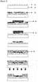
- all of the electrode patterns and the electrode pad unit pattern may be exposed, which is schematically illustrated in FIG. 1 .
- the electrode pad unit pattern may be exposed, which is schematically illustrated in FIG. 2 .
- FIG. 3 the method of manufacturing the electrode substrate for the transparent light emitting device display according to the exemplary embodiment of the present application is schematically illustrated in FIG. 3 .
- an exemplary embodiment of the present application provides an electrode substrate for a transparent light emitting device display, comprising: a transparent base material; an adhesive layer provided on the transparent base material; a copper foil pattern provided on the adhesive layer; and a transparent photosensitive resin composition layer provided on the adhesive layer and the copper foil pattern, in which the transparent photosensitive resin composition layer is not provided in at least a partial region on the copper foil pattern and haze of a region, in which the copper foil pattern is not provided, of the electrode substrate for the transparent light emitting device display is 5% or less.
- Haze of the region, in which the copper foil pattern is not provided, of the electrode substrate for the transparent light emitting device display may be 2% or less, and may be 1% or less.
- the transparent base material contents of the transparent base material, the adhesive layer, the copper foil pattern, the transparent photosensitive resin composition layer, and the like are the same as those described above, so that detailed descriptions thereof will be omitted.
- the electrode substrate for the transparent light emitting device display according to an application of the transparent photosensitive resin composition layer is schematically illustrated in FIG. 5 .
- the transparent photosensitive resin composition layer is formed on the transparent base material and the copper foil pattern, so that it is possible to prevent an increase in haze of the electrode substrate for the transparent light emitting device display due to roughness of the surface of the copper foil, and a refractive index of the transparent photosensitive resin composition layer is adjusted, so that it is possible to decrease haze of the electrode substrate for the transparent light emitting device display.
- the electrode substrate for the transparent light emitting device display according to the exemplary embodiment of the present application may be applied as a transparent electrode of a transparent light emitting device display.
- an exemplary embodiment of the present application provides a transparent light emitting device display comprising the electrode substrate for the transparent light emitting device display.
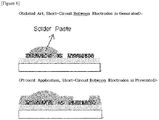
- a short-circuit may be generated between the electrodes during the solder-paste process for mounting the light emitting device on the electrode pad unit pattern.
- the transparent photosensitive resin composition layer during the solder-paste process for mounting the light emitting device on the electrode pad unit pattern.
- a urethane acryl-based transparent adhesive was applied on a PET film having a thickness of 250 ⁇ m by using a comma coater, and then was dried with heat wind at 100°C for five minutes to form an adhesive layer having a thickness of 10 ⁇ m.
- the PET film provided with the transparent adhesive layer and the copper foil having a thickness of 3 ⁇ m were hot-roll laminated under a condition of 120°C and 1.4 (meter per minute (mpm).
- a dry film resist (DFR) was laminated on the copper foil surface of the copper foil laminated film and then a DFR pattern in a Voronoi form having a line width of 20 ⁇ m was formed by exposing and developing processes.
- the exposed copper foil was removed by using a ferric chloride-based copper etchant and the DFR pattern was peeled to form a copper foil pattern in the Voronoi form.
- haze of a region, in which the copper foil pattern is not provided was 40%.
- a negative transparent photosensitive resin composition is applied on a base material, on which the copper foil pattern is provided, by using the comma coater and was dried at 120°C for five minutes to form a negative transparent photosensitive resin composition layer having a thickness of 5 ⁇ m.
- the transparent photosensitive resin composition was prepared by dissolving an acrylate resin of 16 g, of which weightaverage molecular weight is 10,100 g/mol, an acid value is 77 mgKOH/g, a ratio of an acrylic reactor is 30 mol%, dipentaerythritol hexaacrylate of 7.5 g, OXE-02 of 1 g of BASF Company as a photo initiator, and Glide-410 of 0.5 g that is a surfactant in Propylene Glycol Monomethyl Ether Acetate (PGMEA) of 75 g and then filtering the dissolved material by using a filter having a size of 0.1 ⁇ m.
- PMEA Propylene Glycol Monomethyl Ether Acetate
- a rear surface of a surface provided with the transparent photosensitive resin composition layer was radiated with the light amount of 100 mJ/cm 2 by using a parallel light exposure device (Karl Suss MA-8) and then was developed to selectively remove the transparent photosensitive transparent resin composition layer applied on the copper foil pattern.
- haze of a region, in which the copper foil pattern is not provided was 0.8%.
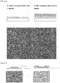
- FIG. 7 A surface, which is in contact with an adhesive layer of the copper foil, a surface of the adhesive layer, from which the copper foil is removed after the forming of the copper foil pattern, and a surface of the transparent photosensitive resin composition layer of Example 1 are illustrated in FIG. 7 .
- the surface, which is in contact with the adhesive layer of the copper foil is formed with nodules in order to maximize adhesive force with the adhesive layer. Further, the nodules are reflected to the surface of the adhesive layer, from which the copper foil is removed after the forming of the copper foil pattern, so that surface roughness of the adhesive layer is increased. Further, it can be seen that after the transparent photosensitive resin composition layer is formed, surface roughness is decreased by the transparent photosensitive resin composition layer.
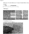
- FIG. 8 a structure, a SEM image, and a transmittance picture of the electrode substrate for the transparent light emitting device display of Example 1 are illustrated in FIG. 8 .
- Example 1 Except that a transparent photosensitive resin composition layer is not formed in Example 1, the method was identically performed to that of Example 1. In this case, haze of a region, in which the copper foil pattern is not provided, was 88.4%.
- FIG. 9 a structure, a SEM image, and a transmittance picture of the electrode substrate for the transparent light emitting device display of Comparative Example 1 are illustrated in FIG. 9 .
- a metal pattern is formed by using low-price copper foil, so that it is possible to decrease raw material cost when an electrode substrate for a transparent light emitting device display is manufactured.
- the transparent photosensitive resin composition layer is formed on the transparent base material and the copper foil pattern, so that it is possible to prevent an increase in haze of the electrode substrate for the transparent light emitting device display due to roughness of the surface of the copper foil, and a refractive index of the transparent photosensitive resin composition layer is adjusted, so that it is possible to decrease haze of the electrode substrate for the transparent light emitting device display.
- At least a part of the copper foil pattern is exposed by removing at least a part of the transparent photosensitive resin composition layer provided on the copper foil pattern, so that it is possible to form an electrode pad unit pattern, which is connected with an external terminal or in which a light emitting device is mounted.
Landscapes
- Engineering & Computer Science (AREA)
- Manufacturing & Machinery (AREA)
- Microelectronics & Electronic Packaging (AREA)
- Electroluminescent Light Sources (AREA)
- Devices For Indicating Variable Information By Combining Individual Elements (AREA)
- Led Device Packages (AREA)
Abstract
Description
- This application claims priority to and the benefit of Korean Patent Application No.
10-2017-0120348 - The present application relates to an electrode substrate for a transparent light emitting device display and a method of manufacturing the same.
- Recently, Korea creates various exterior lighting in parks and town centers, as well as colorful signs, and provides information and attraction to urban residents through the convergence of high-tech information and communication technology (ICT) and light emitting diode (LED) technology. Particularly, in a transparent LED display using an indium tin oxide (ITO) transparent electrode material, an LED is applied between glasses or a transparent film, to which an LED is applied, is attached to one surface of glass, and has an advantage in that wires are not viewed, so that it is possible to display light of high quality. Accordingly, the transparent LED display is utilized in the interior of a hotel, a department store and the like, and has increasing importance in implementing media facade of an exterior wall of a building.
- According to a spread of a smart device, demands of a transparent electrode, which is transparent, is electrically conducted, and is used in a touch screen and the like, are explosive, and the most widely used transparent electrode among the transparent electrodes is an indium tin oxide (ITO) that is an oxide of indium and tin. However, reserves of indium, which is a main raw material of the material of the ITO transparent electrode, are not largely available globally and indium is produced in some countries, such as China, and production cost of indium is high. Further, indium has a disadvantage in that a resistance value is not constantly applied, so that an expressed light beam of an LED is not uniform. Accordingly, the transparent LED utilizing ITO has a limit in being utilized as a transparent electrode material with high performance and low cost.
- It is a fact that the ITO has been most dominantly used as a transparent electrode material, but research and technology development utilizing a new material are continuously conducted due to a limit in economic feasibility, restricted performance, and the like. As a transparent electrode material attracting attention as a next-generation new material, there are metal mesh, an Ag nanowire, carbon nano tube (CNT), conductive polymer, graphene, and the like. Among them, the metal mesh is a new material, which occupies 85% of a material replacing the ITO, is low cost and has high conductivity, so that a market of the metal mesh is expanded in an aspect of utilization of the metal mesh.
- The transparent LED display utilizing the metal mesh is easily repaired and maintained, is capable of saving resources, is capable of considerably preventing environmental contamination, and is economical by a decrease in manufacturing cost, compared to an existing ITO transparent display. Further, the transparent LED display utilizing the metal mesh may be expansively applied for various purposes and may be applied to and utilized in various products as a new transparent electrode material.
- The present application is aimed at providing an electrode substrate for a transparent light emitting device display and a method of manufacturing the same.
- An exemplary embodiment of the present application provides a method of manufacturing an electrode substrate for a transparent light emitting device display, comprising: laminating copper foil on a transparent base material; forming a copper foil pattern by etching the copper foil; forming a transparent photosensitive resin composition layer on a front surface of the transparent base material and the copper foil pattern; and exposing at least a part of the copper foil pattern by removing at least a part of the transparent photosensitive resin composition layer provided on the copper foil pattern.
- Another exemplary embodiment of the present application provides an electrode substrate for a transparent light emitting device display, comprising: a transparent base material; an adhesive layer provided on the transparent base material; a copper foil pattern provided on the adhesive layer; and a transparent photosensitive resin composition layer provided on the adhesive layer and the copper foil pattern, in which the transparent photosensitive resin composition layer is not provided in at least a partial region of the copper foil pattern, and haze of a region, in which the copper foil pattern is not provided, in the electrode substrate for the transparent light emitting device display is 5% or less.
- Still another exemplary embodiment of the present application provides a transparent light emitting device display comprising the electrode substrate for the transparent light emitting device display.
- According to the exemplary embodiment of the present application, a metal pattern is formed by using low-price copper foil, so that it is possible to decrease raw material cost when an electrode substrate for a transparent light emitting device display is manufactured. Particularly, according to the exemplary embodiment of the present application, it is characterized that the transparent photosensitive resin composition layer is formed on the transparent base material and the copper foil pattern, so that it is possible to prevent an increase in haze of the electrode substrate for the transparent light emitting device display due to roughness of the surface of the copper foil, and a refractive index of the transparent photosensitive resin composition layer is adjusted, so that it is possible to decrease haze of the electrode substrate for the transparent light emitting device display.
- Further, according to the exemplary embodiment of the present application, at least a part of the copper foil pattern is exposed by removing at least a part of the transparent photosensitive resin composition layer provided on the copper foil pattern, so that it is possible to form an electrode pad unit pattern, which is connected with an external terminal or in which a light emitting device is mounted.
-
-
FIGS. 1 and 2 are diagrams schematically illustrating an electrode substrate for a transparent light emitting device display according to an exemplary embodiment of the present application. -
FIG. 3 is a diagram schematically illustrating a method of manufacturing an electrode substrate for a transparent light emitting device display according to an exemplary embodiment of the present application. -
FIG. 4 is a diagram schematically illustrating a haze evaluation result according to an application of a transparent photosensitive resin composition layer. -
FIG. 5 is a diagram schematically illustrating the electrode substrate for the transparent light emitting device display according to an application of a transparent photosensitive resin composition layer. -
FIG. 6 is a diagram schematically illustrating a short-circuit between electrodes during a solder paste process of the transparent light emitting device display. -
FIG. 7 is a diagram illustrating a surface, which is in contact with an adhesive layer of copper foil, a surface of the adhesive layer, from which the copper foil is removed after the forming of a copper foil pattern, and a surface of a transparent photosensitive resin composition layer of Example 1. -
FIG. 8 is a diagram illustrating a structure, a SEM image, and a transmittance picture of an electrode substrate for a transparent light emitting device display of Example 1. -
FIG. 9 is a diagram illustrating a structure, a SEM image, and a transmittance picture of an electrode substrate for a transparent light emitting device display of Comparative Example 1. -
- 10: transparent base material
- 20: copper foil
- 30: copper foil pattern
- 40: transparent photosensitive resin layer
- 50: adhesive layer
- 60: resist pattern
- Hereinafter, the present application will be described in detail.
- In the present application, "transparent" is defined to have a transmittance characteristic of about 80% or more in a visible ray region (400 nm to 700 nm).
- In general, a transparent electrode substrate applied to a transparent light emitting diode (LED) display needs to secure a low resistance characteristic of 1 ohm/sq or less, and in order to secure low resistance and high transmittance, a metal layer, such as a Cu layer, of 2 µm or more is required. In the related art, a sputtering method is used for forming the metal layer, but when the sputtering method is used, there is a problem in that it is difficult to secure attachment force between a transparent base material and the metal layer, and a price of the transparent electrode substrate is sharply increased due to an increase in excessive deposition time.
- In this respect, in order to secure price competitiveness, the present application is aimed at providing an electrode substrate for a transparent light emitting device display, which uses very low-cost copper foil as a metal layer, and a method of manufacturing the same.
- A method of manufacturing an electrode substrate for a transparent light emitting device display according to an exemplary embodiment of the present application comprises: laminating copper foil on a transparent base material; forming a copper foil pattern by etching the copper foil; forming a transparent photosensitive resin composition layer on entire surfaces of upper portions of the transparent base material and the copper foil pattern; and exposing at least a part of the copper foil pattern by removing at least a part of the transparent photosensitive resin composition layer provided on the copper foil pattern.
- The method of manufacturing the electrode substrate for the transparent light emitting device display according to the exemplary embodiment of the present application comprises laminating copper foil on a transparent base material.
- The transparent base material may be a glass base material or a transparent plastic base material having excellent transparency, surface smoothness, treatment easiness, and waterproofing property, but is not limited thereto, and as long as a transparent base material is generally used in an electronic device, the transparent substrate is not limited. Particularly, the transparent base material may be a base material formed of glass, a urethane resin, a polyimide resin, a polyester resin, a (meth)acrylate-based polymer resin; a polyolefin-based resin, such as polyethylene or polypropylene, and the like.
- A material known in the art may be used as the copper foil, and a thickness of the copper foil may be 2 µm to 15 µm, but is not limited thereto.
- In the laminating of the copper foil on the transparent base material, an adhesive layer may be used. More particularly, the laminating of the copper foil on the transparent base material may comprise forming an adhesive layer on the transparent base material, and forming a copper foil on the adhesive layer.
- The adhesive layer is positioned between the transparent base material and the copper foil and provides attachment force, and a refractive index of the adhesive layer may be 1.45 to 1.55. More particularly, as the adhesive layer, an acrylic resin, a silicon-based resin, an epoxy-based resin, a polyimide-based resin, and the like having a refractive index of 1.45 to 1.55 are used, and the adhesive layer may be formed in a thickness range of 5 µm to 30 µm by a method, such as comma coating and slot die coating, but the thickness of the adhesive layer is not limited thereto.
- The method of manufacturing the electrode substrate for the transparent light emitting device display according to the exemplary embodiment of the present application comprises forming a copper foil pattern by etching the copper foil.
- As a method of etching the copper foil, a method known in the art may be used. More particularly, the method of etching the copper foil may comprise forming a resist pattern on the copper foil and then etching the copper foil, and peeling the resist pattern, but is not limited thereto.
- The copper foil pattern may comprise two or more kinds of copper foil pattern having different line widths. Further, the copper foil pattern may comprise two kinds of copper foil pattern having different line widths, and a line width of one kind of copper foil pattern is 3 µm to 30 µm, and a line width of the other kind of copper foil pattern is 50 µm or more. The copper foil pattern having the line width of 3 µm to 30 µm may serve as an electrode pattern, and the copper foil pattern having the line width of 50 µm or more may serve as an electrode pad unit pattern for a connection with an external terminal. That is, the copper foil pattern may comprise an electrode pattern and an electrode pad unit pattern. Further, a light emitting device may be mounted on the electrode pad unit pattern.
- A line width of the electrode pattern may be 3 µm to 30 µm, may be 3 µm to 20 µm, and may be 3 µm to 0 µm, but is not limited thereto. Further, a line width of the electrode pad unit pattern may be 50 µm or more, and 50 µm to 100 µm, but is not limited thereto.
- In the exemplary embodiment of the present application, the electrode pattern may comprise a metal mesh pattern. The metal mesh pattern configuring the electrode pattern may have the same line width and the same line height. In the exemplary embodiment of the present application, , the same line width of the metal mesh pattern means that a standard deviation of a line width is 20% or less, preferably, 10% or less, and more preferably, 5% or less. Further, in the exemplary embodiment of the present application, the same line height of the metal mesh pattern means that a standard deviation of a line height is 10% or less, preferably, 5% or less, and more preferably, 2% or less.
- Further, the metal mesh pattern may be provided in the entire region of an effective screen unit on the transparent base material, except for the electrode pad unit pattern. More particularly, the metal mesh pattern may be provided in a region having an area of 80% or more of the entire area of the upper surface of the transparent base material, and may be provided in a region having an area of 99.5% or less. Further, the metal mesh pattern may be provided in a region having an area of 80% or more of an area, in which a FPCB pad unit region and an electrode pad unit pattern region provided on the transparent base material are excluded, based on the entire area of the upper surface of the transparent base material, and may be provided in a region having an area of 99.5% or less. In the present application, the FPCB pad unit region comprises an FPCB pad unit applying external power, and an area of the FPCB pad unit region may be equal to or larger than an entire area of an FPCB pad unit, and be equal to or smaller than three times of the entire area of the FPCB pad unit.
- A pattern form in the art may be used as the metal mesh pattern. More particularly, the metal mesh pattern may comprise a polygonal pattern comprising one or more forms among a triangle, a quadrangle, a pentagon, a hexagon, and an octagon. The metal mesh pattern may comprise a straight line, a curve, or a closed curve formed of a straight line or a curve.
- Further, the transparent photosensitive resin composition layer may be provided on the electrode pattern, and the transparent photosensitive resin composition layer may not be provided on at least a part of the electrode pad unit pattern.
- The method of manufacturing the electrode substrate for the transparent light emitting device display according to the exemplary embodiment of the present application comprises forming a transparent photosensitive resin composition layer on entire surfaces of upper surfaces of the transparent base material and the copper foil pattern. The transparent photosensitive resin composition layer may be formed by applying a transparent photosensitive resin composition on entire surfaces of upper surfaces of the transparent base material and the copper foil pattern.
- When the adhesive layer is provided on the transparent base material and then the low-price copper foil is laminated, surface roughness of the copper foil is transferred to a surface of the adhesive layer, so that there may be a problem in that haze of a final product is increased. In order to decrease surface roughness of the adhesive layer, a method of additionally applying a transparent resin having a similar refractive index to that of the adhesive layer onto the adhesive layer may be considered, but in this case, there may be a problem in that the electrode pad unit pattern for the connection with the external terminal or for the mounting of the light emitting device is insulated by a transparent resin layer. Accordingly, in the present application, the transparent photosensitive resin composition layer having photosensitivity is formed on the entire surfaces of the upper portions of the transparent base material and the copper foil pattern, so that it is possible to decrease surface roughness of the adhesive layer, and there is a characteristic in that the electrode pad unit pattern for the connection with the external terminal or for the mounting of the light emitting device may be exposed by removing at least a part of the transparent photosensitive resin composition layer by rear surface exposing and developing methods, which will be described below.
- The transparent photosensitive resin composition is a negative-type transparent photosensitive resin composition, and a difference in a refractive index between the transparent photosensitive resin composition and the adhesive layer provided on the transparent base material may be within 0.05, and preferably, within 0.02. More particularly, as the transparent photosensitive resin composition, an acryl-based UV hardening resin having a refractive index of 1.45 to 1.52 may be used.
- A thickness of the transparent photosensitive resin composition layer may be different according to a thickness of the copper foil pattern provided on the adhesive layer. More particularly, a thickness of the transparent photosensitive resin composition layer may have a difference of within 10 µm with a thickness of the copper foil pattern in consideration of easiness of a post-process, such as the LED mounting and the FPCB bonding. For example, when a thickness of the copper foil pattern is 5 µm or less, a thickness of the transparent photosensitive resin composition layer may be 15 µm or less. When a difference in a thickness between the copper foil pattern and the transparent photosensitive resin composition layer is larger than 10 µm, a possibility in that the LED is damaged is high when clearance is generated during the process of mounting the LED, and pressure is not transmitted to a conductive ball when a step is excessively generated during the FPCB bonding, so that there may be a problem in that it is impossible to carry an electric current.
- A haze evaluation result according to an application of the transparent photosensitive resin composition layer is schematically illustrated in
FIG. 4 . When the transparent photosensitive resin composition layer is not applied as illustrated inFIG. 4 , it can be seen that roughness of the surface of the copper foil is transferred to the adhesive layer, so that haze is increased, and when the transparent photosensitive resin composition layer is applied like the present application, it can be seen that haze is decreased through the matching of the refractive indexes of the transparent photosensitive resin composition layer and the adhesive layer. - The method of manufacturing the electrode substrate for the transparent light emitting device display according to the exemplary embodiment of the present application comprises exposing at least a part of the copper foil pattern by removing at least a part of the transparent photosensitive resin composition layer provided on the copper foil pattern.
- The removing at least a part of the transparent photosensitive resin composition layer provided on the copper foil pattern may comprise performing rear-surface exposing and developing on a lower surface of the transparent base material.
- When the rear-surface exposing is performed on the lower surface of the transparent base material, the copper foil pattern provided on the adhesive layer serves as a photomask, so that a separate photomask is not necessary, and it is possible to fundamentally remove the generation of a fault due to an alignment error.
- In the rear-surface exposing, parallel light exposing or scattered light exposing may be performed. When the parallel light exposing is performed during the rear-surface exposing, all of the electrode patterns and the electrode pad unit pattern may be exposed, which is schematically illustrated in
FIG. 1 . Further, when the scattered light exposing is performed during the rear-surface exposing, the electrode pad unit pattern may be exposed, which is schematically illustrated inFIG. 2 . - Further, the method of manufacturing the electrode substrate for the transparent light emitting device display according to the exemplary embodiment of the present application is schematically illustrated in
FIG. 3 . - Further, an exemplary embodiment of the present application provides an electrode substrate for a transparent light emitting device display, comprising: a transparent base material; an adhesive layer provided on the transparent base material; a copper foil pattern provided on the adhesive layer; and a transparent photosensitive resin composition layer provided on the adhesive layer and the copper foil pattern, in which the transparent photosensitive resin composition layer is not provided in at least a partial region on the copper foil pattern and haze of a region, in which the copper foil pattern is not provided, of the electrode substrate for the transparent light emitting device display is 5% or less.
- Haze of the region, in which the copper foil pattern is not provided, of the electrode substrate for the transparent light emitting device display may be 2% or less, and may be 1% or less.
- In the electrode substrate for the transparent light emitting device display according to the exemplary embodiment of the present application, contents of the transparent base material, the adhesive layer, the copper foil pattern, the transparent photosensitive resin composition layer, and the like are the same as those described above, so that detailed descriptions thereof will be omitted.
- The electrode substrate for the transparent light emitting device display according to an application of the transparent photosensitive resin composition layer is schematically illustrated in
FIG. 5 . As illustrated inFIG. 5 , according to the exemplary embodiment of the present application, it is characterized that the transparent photosensitive resin composition layer is formed on the transparent base material and the copper foil pattern, so that it is possible to prevent an increase in haze of the electrode substrate for the transparent light emitting device display due to roughness of the surface of the copper foil, and a refractive index of the transparent photosensitive resin composition layer is adjusted, so that it is possible to decrease haze of the electrode substrate for the transparent light emitting device display. - The electrode substrate for the transparent light emitting device display according to the exemplary embodiment of the present application may be applied as a transparent electrode of a transparent light emitting device display.
- Further, an exemplary embodiment of the present application provides a transparent light emitting device display comprising the electrode substrate for the transparent light emitting device display.
- As illustrated in
FIG. 6 , in the transparent light emitting device display in the related art, a short-circuit may be generated between the electrodes during the solder-paste process for mounting the light emitting device on the electrode pad unit pattern. However, according to the exemplary embodiment of the present application, there is a characteristic in that it is possible to prevent a short-circuit between the electrodes by the transparent photosensitive resin composition layer during the solder-paste process for mounting the light emitting device on the electrode pad unit pattern. - Hereinafter, the exemplary embodiment described in the present specification will be exemplified through Examples. However, this does not intend to limit the range of the exemplary embodiments by Examples.
- A urethane acryl-based transparent adhesive was applied on a PET film having a thickness of 250 µm by using a comma coater, and then was dried with heat wind at 100°C for five minutes to form an adhesive layer having a thickness of 10 µm. The PET film provided with the transparent adhesive layer and the copper foil having a thickness of 3 µm were hot-roll laminated under a condition of 120°C and 1.4 (meter per minute (mpm).
- A dry film resist (DFR) was laminated on the copper foil surface of the copper foil laminated film and then a DFR pattern in a Voronoi form having a line width of 20 µm was formed by exposing and developing processes.
- The exposed copper foil was removed by using a ferric chloride-based copper etchant and the DFR pattern was peeled to form a copper foil pattern in the Voronoi form. In this case, haze of a region, in which the copper foil pattern is not provided, was 40%.
- A negative transparent photosensitive resin composition is applied on a base material, on which the copper foil pattern is provided, by using the comma coater and was dried at 120°C for five minutes to form a negative transparent photosensitive resin composition layer having a thickness of 5 µm.
- The transparent photosensitive resin composition was prepared by dissolving an acrylate resin of 16 g, of which weightaverage molecular weight is 10,100 g/mol, an acid value is 77 mgKOH/g, a ratio of an acrylic reactor is 30 mol%, dipentaerythritol hexaacrylate of 7.5 g, OXE-02 of 1 g of BASF Company as a photo initiator, and Glide-410 of 0.5 g that is a surfactant in Propylene Glycol Monomethyl Ether Acetate (PGMEA) of 75 g and then filtering the dissolved material by using a filter having a size of 0.1 µm.
- A rear surface of a surface provided with the transparent photosensitive resin composition layer was radiated with the light amount of 100 mJ/cm2 by using a parallel light exposure device (Karl Suss MA-8) and then was developed to selectively remove the transparent photosensitive transparent resin composition layer applied on the copper foil pattern. In this case, haze of a region, in which the copper foil pattern is not provided, was 0.8%.
- A surface, which is in contact with an adhesive layer of the copper foil, a surface of the adhesive layer, from which the copper foil is removed after the forming of the copper foil pattern, and a surface of the transparent photosensitive resin composition layer of Example 1 are illustrated in
FIG. 7 . As illustrated inFIG. 7 , the surface, which is in contact with the adhesive layer of the copper foil, is formed with nodules in order to maximize adhesive force with the adhesive layer. Further, the nodules are reflected to the surface of the adhesive layer, from which the copper foil is removed after the forming of the copper foil pattern, so that surface roughness of the adhesive layer is increased. Further, it can be seen that after the transparent photosensitive resin composition layer is formed, surface roughness is decreased by the transparent photosensitive resin composition layer. - Further, a structure, a SEM image, and a transmittance picture of the electrode substrate for the transparent light emitting device display of Example 1 are illustrated in
FIG. 8 . - Except that a transparent photosensitive resin composition layer is not formed in Example 1, the method was identically performed to that of Example 1. In this case, haze of a region, in which the copper foil pattern is not provided, was 88.4%.
- Further, a structure, a SEM image, and a transmittance picture of the electrode substrate for the transparent light emitting device display of Comparative Example 1 are illustrated in
FIG. 9 . - As can be seen in the result, according to the exemplary embodiment of the present application, a metal pattern is formed by using low-price copper foil, so that it is possible to decrease raw material cost when an electrode substrate for a transparent light emitting device display is manufactured. Particularly, according to the exemplary embodiment of the present application, it is characterized that the transparent photosensitive resin composition layer is formed on the transparent base material and the copper foil pattern, so that it is possible to prevent an increase in haze of the electrode substrate for the transparent light emitting device display due to roughness of the surface of the copper foil, and a refractive index of the transparent photosensitive resin composition layer is adjusted, so that it is possible to decrease haze of the electrode substrate for the transparent light emitting device display.
- Further, according to the exemplary embodiment of the present application, at least a part of the copper foil pattern is exposed by removing at least a part of the transparent photosensitive resin composition layer provided on the copper foil pattern, so that it is possible to form an electrode pad unit pattern, which is connected with an external terminal or in which a light emitting device is mounted.
Claims (21)
- A method of manufacturing an electrode substrate for a transparent light emitting device display, the method comprising:laminating copper foil on a transparent base material;forming a copper foil pattern by etching the copper foil;forming a transparent photosensitive resin composition layer on entire surfaces of upper portions of the transparent base material and the copper foil pattern; andexposing at least a part of the copper foil pattern by removing at least a part of the transparent photosensitive resin composition layer provided on the copper foil pattern.
- The method of claim 1, wherein a thickness of the copper foil is 2 µm to 15 µm.
- The method of claim 1, wherein the laminating of the copper foil on the transparent base material uses an adhesive layer.
- The method of claim 3, wherein a refractive index of the adhesive layer is 1.45 to 1.55.
- The method of claim 3, wherein a thickness of the adhesive layer is 5 µm to 30 µm.
- The method of claim 1, wherein a refractive index of the transparent photosensitive resin composition layer is 1.45 to 1.55.
- The method of claim 3, wherein a difference in a refractive index between the adhesive layer and the transparent photosensitive resin composition layer is within 0.05.
- The method of claim 1, wherein a difference in a thickness between the transparent photosensitive resin composition layer and the copper foil pattern is within 10 µm.
- The method of claim 1, wherein the removing of at least the part of the transparent photosensitive resin composition layer provided on the copper foil pattern comprises performing rear-surface exposing and developing on a lower surface of the transparent base material.
- The method of claim 1, wherein the copper foil pattern comprises two or more kinds of copper foil pattern having different line widths.
- The method of claim 10, wherein the copper foil pattern comprises an electrode pattern and an electrode pad unit pattern,
a line width of the electrode pattern is 3 µm to 30 µm, and
a line width of the electrode pad unit pattern is 50 µm or more. - The method of claim 11, wherein the electrode pattern comprises a metal mesh pattern, and
the metal mesh pattern is provided on an entire region of an effective screen unit on the transparent base material, except for the electrode pad unit pattern. - The method of claim 11, wherein the transparent photosensitive resin composition layer is provided on the electrode pattern, and
the transparent photosensitive resin composition layer is not provided on at least a part of the electrode pad unit pattern. - An electrode substrate for a transparent light emitting device display, the electrode substrate comprising
a transparent base material;
an adhesive layer provided on the transparent base material;
a copper foil pattern provided on the adhesive layer; and
a transparent photosensitive resin composition layer provided on the adhesive layer and the copper foil pattern,
wherein the transparent photosensitive resin composition layer is not provided in at least a partial region of the copper foil pattern, and
haze of a region, in which the copper foil pattern is not provided, in the electrode substrate for the transparent light emitting device display is 5% or less. - The electrode substrate of claim 14, wherein a difference in a refractive index between the adhesive layer and the transparent photosensitive resin composition layer is within 0.05.
- The electrode substrate of claim 14, wherein a difference in a thickness between the transparent photosensitive resin composition layer and the copper foil pattern is within 10 µm.
- The electrode substrate of claim 14, wherein haze of the region, in which the copper foil pattern is not provided, in the electrode substrate for the transparent light emitting device display is 2% or less.
- The electrode substrate of claim 14, wherein the copper foil pattern comprises an electrode pattern and an electrode pad unit pattern, a line width of the electrode pattern is 3 µm to 30 µm, and
a line width of the electrode pad unit pattern is 50 µm or more. - The electrode substrate of claim 18, wherein the electrode pattern comprises a metal mesh pattern, and
the metal mesh pattern is provided on an entire region of an effective screen unit on the transparent base material, except for the electrode pad unit pattern. - The electrode substrate of claim 18, wherein the transparent photosensitive resin composition layer is provided on the electrode pattern, and
the transparent photosensitive resin composition layer is not provided on at least a part of the electrode pad unit pattern. - A transparent light emitting device display comprising the electrode substrate for the transparent light emitting device display of any one of claims 14 to 20.
Applications Claiming Priority (2)
| Application Number | Priority Date | Filing Date | Title |
|---|---|---|---|
| KR20170120348 | 2017-09-19 | ||
| PCT/KR2018/010830 WO2019059589A1 (en) | 2017-09-19 | 2018-09-14 | Electrode substrate for transparent light-emitting device display, and manufacturing method therefor |
Publications (3)
| Publication Number | Publication Date |
|---|---|
| EP3686905A1 true EP3686905A1 (en) | 2020-07-29 |
| EP3686905A4 EP3686905A4 (en) | 2020-11-04 |
| EP3686905B1 EP3686905B1 (en) | 2026-05-06 |
Family
ID=65811347
Family Applications (1)
| Application Number | Title | Priority Date | Filing Date |
|---|---|---|---|
| EP18857644.1A Active EP3686905B1 (en) | 2017-09-19 | 2018-09-14 | Method of manufacturing electrode substrate for transparent light-emitting device display |
Country Status (7)
| Country | Link |
|---|---|
| US (1) | US10868229B2 (en) |
| EP (1) | EP3686905B1 (en) |
| JP (1) | JP6821060B2 (en) |
| KR (1) | KR102129675B1 (en) |
| CN (1) | CN110637345B (en) |
| TW (1) | TWI675244B (en) |
| WO (1) | WO2019059589A1 (en) |
Families Citing this family (8)
| Publication number | Priority date | Publication date | Assignee | Title |
|---|---|---|---|---|
| US11063525B2 (en) * | 2019-01-07 | 2021-07-13 | Delta Electronics (Shanghai) Co., Ltd. | Power supply module and manufacture method for same |
| CN113630982A (en) * | 2020-05-07 | 2021-11-09 | 深圳市晶泓科技有限公司 | Transparent LED circuit board and preparation method of transparent LED display screen |
| CN112752413B (en) * | 2020-12-03 | 2022-05-31 | 深圳市晶泓科技有限公司 | Transparent LED circuit board and preparation method of transparent LED display screen |
| KR102879737B1 (en) * | 2021-05-24 | 2025-11-11 | 주식회사 에이피에스 | Method for forming metal pattern |
| WO2025143924A1 (en) * | 2023-12-29 | 2025-07-03 | 동우 화인켐 주식회사 | Optical laminate, transparent display comprising same, and manufacturing method therefor |
| KR102807618B1 (en) * | 2023-12-29 | 2025-05-19 | 동우 화인켐 주식회사 | OPTICAL LAMINATE, transparent display COMPRISING THE SAME, AND MANUFACTURING METHOD FOR THE SAME |
| KR102730429B1 (en) * | 2024-01-22 | 2024-11-15 | 주식회사 에이지에이세미콘 | Method for connecting electrode pads of micro led and display apparatus manufactured by the same |
| KR102897288B1 (en) | 2025-03-11 | 2025-12-08 | 동우 화인켐 주식회사 | Transparent display panel, display device comprising the same, and manufacturing method for the same |
Family Cites Families (32)
| Publication number | Priority date | Publication date | Assignee | Title |
|---|---|---|---|---|
| JP2653458B2 (en) * | 1988-03-26 | 1997-09-17 | 旭化成工業株式会社 | Photosensitive resin composition for letterpress printing plates |
| JPH09270573A (en) * | 1996-03-29 | 1997-10-14 | Cmk Corp | Printed wiring board and manufacturing method thereof |
| JPH10282513A (en) | 1997-04-07 | 1998-10-23 | Sharp Corp | Method for manufacturing electrode substrate and liquid crystal display element |
| JPH10335064A (en) * | 1997-05-19 | 1998-12-18 | Minnesota Mining & Mfg Co <3M> | Electroluminescent element and its manufacture |
| US6567148B1 (en) * | 1998-09-10 | 2003-05-20 | Sharp Kabushiki Kaisha | Electrode substrate having particular projecting portion, manufacturing method thereof, and liquid crystal display element |
| KR100326535B1 (en) | 1999-02-09 | 2002-03-25 | 구자홍 | Electrodes Of Plasma Display Panel And Fabrication Method Thereof |
| KR101284982B1 (en) | 2006-10-31 | 2013-07-17 | 히타치가세이가부시끼가이샤 | Resin composition for optical use, resin material for optical use using the same, optical filter for image display device, and image display device |
| JP2009200432A (en) * | 2008-02-25 | 2009-09-03 | Sumitomo Metal Mining Co Ltd | Flexible wiring substrate and its manufacturing method |
| KR100992187B1 (en) * | 2008-08-28 | 2010-11-04 | 삼성전기주식회사 | Printed Circuit Board and Manufacturing Method Thereof |
| JP2011114194A (en) | 2009-11-27 | 2011-06-09 | Alps Electric Co Ltd | Method of forming transparent electrode pattern |
| GB201105364D0 (en) | 2011-03-30 | 2011-05-11 | Cambridge Display Tech Ltd | Surface planarisation |
| KR20120138287A (en) | 2011-06-14 | 2012-12-26 | 삼성전기주식회사 | Touch panel and method of manufacturing the same |
| CN102315290B (en) * | 2011-09-23 | 2013-01-30 | 中国科学院光电技术研究所 | Full-spectrum absorption enhanced hydrogenated amorphous silicon thin-film solar cell |
| WO2014200312A1 (en) * | 2013-06-14 | 2014-12-18 | 주식회사 엘지화학 | Organic photovoltaic cell and method for manufacturing same |
| AU2014310703B2 (en) * | 2013-08-19 | 2018-09-27 | Basf Se | Optical detector |
| KR20150033169A (en) | 2013-09-23 | 2015-04-01 | 엘지디스플레이 주식회사 | Light emitting diode package and liquid crystal display device using the same |
| US9880461B2 (en) | 2014-02-13 | 2018-01-30 | Lg Chem, Ltd. | Method for manufacturing master mold, master mold manufactured thereby, method for manufacturing transparent photomask, transparent photomask manufactured thereby, and method for forming conductive mesh pattern using transparent photomask |
| JP2015157392A (en) * | 2014-02-24 | 2015-09-03 | パナソニックIpマネジメント株式会社 | Laminate for see-through type electrode and production method for the same, see-through type electrode material and device |
| JP6333780B2 (en) | 2014-08-12 | 2018-05-30 | 富士フイルム株式会社 | Transfer film, transfer film manufacturing method, laminate, laminate manufacturing method, capacitive input device, and image display device |
| KR101791299B1 (en) * | 2014-09-29 | 2017-10-27 | 주식회사 엘지화학 | method for manufacturing a electrode comprising auxiliary electrode through roll-to-roll consecutive process, electrode manufactured by the same, and electric device comprising the same |
| WO2016088609A1 (en) * | 2014-12-03 | 2016-06-09 | 富士フイルム株式会社 | Transfer film, manufacturing method for film sensor, film sensor, front-plate-integrated-type sensor, and image display apparatus |
| JP6230559B2 (en) * | 2014-12-03 | 2017-11-15 | 富士フイルム株式会社 | Transfer film, film sensor manufacturing method, film sensor, front plate integrated sensor, and image display device |
| EP3035122B1 (en) * | 2014-12-16 | 2019-03-20 | ATOTECH Deutschland GmbH | Method for fine line manufacturing |
| KR101784406B1 (en) * | 2015-02-25 | 2017-10-12 | 금호전기주식회사 | Transparent light emitting apparatus |
| KR20160126192A (en) * | 2015-04-23 | 2016-11-02 | 대덕지디에스 주식회사 | Method of manufacturing transparent printed circuit board |
| JP6620464B2 (en) | 2015-08-26 | 2019-12-18 | 大日本印刷株式会社 | Flexible transparent substrate and see-through type LED display device using the same |
| KR20170029838A (en) | 2015-09-08 | 2017-03-16 | 재단법인대구경북과학기술원 | Conducting film, method for preparing the same and electrode comprising the same |
| CN107001885B (en) * | 2015-11-05 | 2019-03-08 | 株式会社Lg化学 | Adhesive composition for optical applications and adhesive film for optical applications |
| JP6807864B2 (en) | 2015-11-27 | 2021-01-06 | 三井金属鉱業株式会社 | Manufacturing method of resin laminate with wiring pattern |
| JP6833722B2 (en) * | 2015-12-28 | 2021-02-24 | 東芝ホクト電子株式会社 | Luminous module |
| KR20170120348A (en) | 2016-04-21 | 2017-10-31 | 주식회사 씨엔플러스 | Plug Connector Assembly |
| JP2018017996A (en) * | 2016-07-29 | 2018-02-01 | 日東電工株式会社 | Polarizing plate with retardation layer and organic EL display device |
-
2018
- 2018-09-14 KR KR1020180110118A patent/KR102129675B1/en active Active
- 2018-09-14 US US16/619,056 patent/US10868229B2/en active Active
- 2018-09-14 JP JP2019563208A patent/JP6821060B2/en active Active
- 2018-09-14 CN CN201880031975.7A patent/CN110637345B/en active Active
- 2018-09-14 EP EP18857644.1A patent/EP3686905B1/en active Active
- 2018-09-14 WO PCT/KR2018/010830 patent/WO2019059589A1/en not_active Ceased
- 2018-09-18 TW TW107132717A patent/TWI675244B/en active
Also Published As
| Publication number | Publication date |
|---|---|
| KR102129675B1 (en) | 2020-07-02 |
| KR20190032212A (en) | 2019-03-27 |
| TWI675244B (en) | 2019-10-21 |
| EP3686905A4 (en) | 2020-11-04 |
| CN110637345A (en) | 2019-12-31 |
| US10868229B2 (en) | 2020-12-15 |
| JP2020523623A (en) | 2020-08-06 |
| CN110637345B (en) | 2021-10-29 |
| US20200091392A1 (en) | 2020-03-19 |
| EP3686905B1 (en) | 2026-05-06 |
| TW201921066A (en) | 2019-06-01 |
| WO2019059589A1 (en) | 2019-03-28 |
| JP6821060B2 (en) | 2021-01-27 |
Similar Documents
| Publication | Publication Date | Title |
|---|---|---|
| US10868229B2 (en) | Electrode substrate for transparent light-emitting device display, and manufacturing method therefor | |
| EP3651216B1 (en) | Embedded electrode substrate for transparent light-emitting element display, and method for manufacturing same | |
| KR102129674B1 (en) | Electrode substrate for transparent light emitting device display and method for manufacturing thereof | |
| CN105335034B (en) | Two-sided capacitance plate functional sheet of metal grill monofilm and preparation method thereof | |
| US11716818B2 (en) | Embedded-type transparent electrode substrate and method for manufacturing same | |
| JP7233802B2 (en) | Transparent light-emitting element display | |
| KR20180045712A (en) | Method for manufacturing sensor for touch screen sensor, and sensor for touch screen panel | |
| CN202841679U (en) | ITO conducting film-based bus electrode | |
| JP5333142B2 (en) | Pattern electrode, organic electroluminescence element, and method of manufacturing pattern electrode | |
| CN109155167B (en) | Translucent conductive film and method for producing translucent conductive film having patterned conductive layer | |
| KR102361783B1 (en) | Embedded transparent electrode substrate and method for manufacturing thereof | |
| KR20200024472A (en) | Embedded electrode substrate and method for manufacturing thereof | |
| JP2014188730A (en) | Transparent conductive laminate, and method of producing transparent conductive laminate |
Legal Events
| Date | Code | Title | Description |
|---|---|---|---|
| STAA | Information on the status of an ep patent application or granted ep patent |
Free format text: STATUS: THE INTERNATIONAL PUBLICATION HAS BEEN MADE |
|
| PUAI | Public reference made under article 153(3) epc to a published international application that has entered the european phase |
Free format text: ORIGINAL CODE: 0009012 |
|
| STAA | Information on the status of an ep patent application or granted ep patent |
Free format text: STATUS: REQUEST FOR EXAMINATION WAS MADE |
|
| 17P | Request for examination filed |
Effective date: 20191104 |
|
| AK | Designated contracting states |
Kind code of ref document: A1 Designated state(s): AL AT BE BG CH CY CZ DE DK EE ES FI FR GB GR HR HU IE IS IT LI LT LU LV MC MK MT NL NO PL PT RO RS SE SI SK SM TR |
|
| AX | Request for extension of the european patent |
Extension state: BA ME |
|
| A4 | Supplementary search report drawn up and despatched |
Effective date: 20201005 |
|
| RIC1 | Information provided on ipc code assigned before grant |
Ipc: H05K 1/02 20060101ALI20200929BHEP Ipc: H01L 33/62 20100101ALI20200929BHEP Ipc: H05K 3/00 20060101ALI20200929BHEP Ipc: H01L 27/15 20060101ALI20200929BHEP Ipc: H01L 25/075 20060101ALI20200929BHEP Ipc: H01L 33/02 20100101ALI20200929BHEP Ipc: H05K 3/34 20060101ALI20200929BHEP Ipc: H01L 21/02 20060101ALI20200929BHEP Ipc: H05K 3/06 20060101ALI20200929BHEP Ipc: H01B 13/00 20060101AFI20200929BHEP Ipc: H01L 33/42 20100101ALI20200929BHEP |
|
| DAV | Request for validation of the european patent (deleted) | ||
| DAX | Request for extension of the european patent (deleted) | ||
| STAA | Information on the status of an ep patent application or granted ep patent |
Free format text: STATUS: EXAMINATION IS IN PROGRESS |
|
| 17Q | First examination report despatched |
Effective date: 20220504 |
|
| REG | Reference to a national code |
Ref country code: DE Ref legal event code: R079 Free format text: PREVIOUS MAIN CLASS: H01B0013000000 Ipc: H05K0003000000 Ref country code: DE Ref legal event code: R079 Ref document number: 602018091220 Country of ref document: DE Free format text: PREVIOUS MAIN CLASS: H01B0013000000 Ipc: H05K0003000000 |
|
| GRAP | Despatch of communication of intention to grant a patent |
Free format text: ORIGINAL CODE: EPIDOSNIGR1 |
|
| STAA | Information on the status of an ep patent application or granted ep patent |
Free format text: STATUS: GRANT OF PATENT IS INTENDED |
|
| RIC1 | Information provided on ipc code assigned before grant |
Ipc: H05K 3/00 20060101AFI20260115BHEP Ipc: H10H 20/01 20250101ALI20260115BHEP Ipc: H10H 20/857 20250101ALI20260115BHEP Ipc: H05K 3/34 20060101ALN20260115BHEP |
|
| INTG | Intention to grant announced |
Effective date: 20260122 |
|
| GRAS | Grant fee paid |
Free format text: ORIGINAL CODE: EPIDOSNIGR3 |
|
| GRAA | (expected) grant |
Free format text: ORIGINAL CODE: 0009210 |
|
| STAA | Information on the status of an ep patent application or granted ep patent |
Free format text: STATUS: THE PATENT HAS BEEN GRANTED |