EP3683840A2 - Anzeigevorrichtung - Google Patents
Anzeigevorrichtung Download PDFInfo
- Publication number
- EP3683840A2 EP3683840A2 EP20150643.3A EP20150643A EP3683840A2 EP 3683840 A2 EP3683840 A2 EP 3683840A2 EP 20150643 A EP20150643 A EP 20150643A EP 3683840 A2 EP3683840 A2 EP 3683840A2
- Authority
- EP
- European Patent Office
- Prior art keywords
- light
- emitting device
- layer
- pixel
- pixel region
- Prior art date
- Legal status (The legal status is an assumption and is not a legal conclusion. Google has not performed a legal analysis and makes no representation as to the accuracy of the status listed.)
- Granted
Links
Images








Classifications
-
- H—ELECTRICITY
- H10—SEMICONDUCTOR DEVICES; ELECTRIC SOLID-STATE DEVICES NOT OTHERWISE PROVIDED FOR
- H10K—ORGANIC ELECTRIC SOLID-STATE DEVICES
- H10K50/00—Organic light-emitting devices
- H10K50/10—OLEDs or polymer light-emitting diodes [PLED]
- H10K50/11—OLEDs or polymer light-emitting diodes [PLED] characterised by the electroluminescent [EL] layers
- H10K50/125—OLEDs or polymer light-emitting diodes [PLED] characterised by the electroluminescent [EL] layers specially adapted for multicolour light emission, e.g. for emitting white light
- H10K50/13—OLEDs or polymer light-emitting diodes [PLED] characterised by the electroluminescent [EL] layers specially adapted for multicolour light emission, e.g. for emitting white light comprising stacked EL layers within one EL unit
-
- H—ELECTRICITY
- H10—SEMICONDUCTOR DEVICES; ELECTRIC SOLID-STATE DEVICES NOT OTHERWISE PROVIDED FOR
- H10K—ORGANIC ELECTRIC SOLID-STATE DEVICES
- H10K59/00—Integrated devices, or assemblies of multiple devices, comprising at least one organic light-emitting element covered by group H10K50/00
- H10K59/30—Devices specially adapted for multicolour light emission
- H10K59/35—Devices specially adapted for multicolour light emission comprising red-green-blue [RGB] subpixels
-
- H—ELECTRICITY
- H10—SEMICONDUCTOR DEVICES; ELECTRIC SOLID-STATE DEVICES NOT OTHERWISE PROVIDED FOR
- H10K—ORGANIC ELECTRIC SOLID-STATE DEVICES
- H10K59/00—Integrated devices, or assemblies of multiple devices, comprising at least one organic light-emitting element covered by group H10K50/00
- H10K59/10—OLED displays
- H10K59/12—Active-matrix OLED [AMOLED] displays
- H10K59/121—Active-matrix OLED [AMOLED] displays characterised by the geometry or disposition of pixel elements
-
- H—ELECTRICITY
- H10—SEMICONDUCTOR DEVICES; ELECTRIC SOLID-STATE DEVICES NOT OTHERWISE PROVIDED FOR
- H10K—ORGANIC ELECTRIC SOLID-STATE DEVICES
- H10K59/00—Integrated devices, or assemblies of multiple devices, comprising at least one organic light-emitting element covered by group H10K50/00
- H10K59/10—OLED displays
- H10K59/12—Active-matrix OLED [AMOLED] displays
- H10K59/121—Active-matrix OLED [AMOLED] displays characterised by the geometry or disposition of pixel elements
- H10K59/1213—Active-matrix OLED [AMOLED] displays characterised by the geometry or disposition of pixel elements the pixel elements being TFTs
-
- H—ELECTRICITY
- H10—SEMICONDUCTOR DEVICES; ELECTRIC SOLID-STATE DEVICES NOT OTHERWISE PROVIDED FOR
- H10K—ORGANIC ELECTRIC SOLID-STATE DEVICES
- H10K59/00—Integrated devices, or assemblies of multiple devices, comprising at least one organic light-emitting element covered by group H10K50/00
- H10K59/10—OLED displays
- H10K59/12—Active-matrix OLED [AMOLED] displays
- H10K59/122—Pixel-defining structures or layers, e.g. banks
-
- H—ELECTRICITY
- H10—SEMICONDUCTOR DEVICES; ELECTRIC SOLID-STATE DEVICES NOT OTHERWISE PROVIDED FOR
- H10K—ORGANIC ELECTRIC SOLID-STATE DEVICES
- H10K59/00—Integrated devices, or assemblies of multiple devices, comprising at least one organic light-emitting element covered by group H10K50/00
- H10K59/30—Devices specially adapted for multicolour light emission
- H10K59/32—Stacked devices having two or more layers, each emitting at different wavelengths
-
- H—ELECTRICITY
- H10—SEMICONDUCTOR DEVICES; ELECTRIC SOLID-STATE DEVICES NOT OTHERWISE PROVIDED FOR
- H10K—ORGANIC ELECTRIC SOLID-STATE DEVICES
- H10K59/00—Integrated devices, or assemblies of multiple devices, comprising at least one organic light-emitting element covered by group H10K50/00
- H10K59/90—Assemblies of multiple devices comprising at least one organic light-emitting element
-
- H—ELECTRICITY
- H10—SEMICONDUCTOR DEVICES; ELECTRIC SOLID-STATE DEVICES NOT OTHERWISE PROVIDED FOR
- H10K—ORGANIC ELECTRIC SOLID-STATE DEVICES
- H10K71/00—Manufacture or treatment specially adapted for the organic devices covered by this subclass
-
- H—ELECTRICITY
- H10—SEMICONDUCTOR DEVICES; ELECTRIC SOLID-STATE DEVICES NOT OTHERWISE PROVIDED FOR
- H10W—GENERIC PACKAGES, INTERCONNECTIONS, CONNECTORS OR OTHER CONSTRUCTIONAL DETAILS OF DEVICES COVERED BY CLASS H10
- H10W90/00—Package configurations
-
- H—ELECTRICITY
- H10—SEMICONDUCTOR DEVICES; ELECTRIC SOLID-STATE DEVICES NOT OTHERWISE PROVIDED FOR
- H10K—ORGANIC ELECTRIC SOLID-STATE DEVICES
- H10K2102/00—Constructional details relating to the organic devices covered by this subclass
- H10K2102/301—Details of OLEDs
- H10K2102/351—Thickness
-
- H—ELECTRICITY
- H10—SEMICONDUCTOR DEVICES; ELECTRIC SOLID-STATE DEVICES NOT OTHERWISE PROVIDED FOR
- H10K—ORGANIC ELECTRIC SOLID-STATE DEVICES
- H10K59/00—Integrated devices, or assemblies of multiple devices, comprising at least one organic light-emitting element covered by group H10K50/00
- H10K59/80—Constructional details
- H10K59/87—Passivation; Containers; Encapsulations
- H10K59/873—Encapsulations
-
- H—ELECTRICITY
- H10—SEMICONDUCTOR DEVICES; ELECTRIC SOLID-STATE DEVICES NOT OTHERWISE PROVIDED FOR
- H10K—ORGANIC ELECTRIC SOLID-STATE DEVICES
- H10K71/00—Manufacture or treatment specially adapted for the organic devices covered by this subclass
- H10K71/20—Changing the shape of the active layer in the devices, e.g. patterning
- H10K71/211—Changing the shape of the active layer in the devices, e.g. patterning by selective transformation of an existing layer
-
- H—ELECTRICITY
- H10—SEMICONDUCTOR DEVICES; ELECTRIC SOLID-STATE DEVICES NOT OTHERWISE PROVIDED FOR
- H10K—ORGANIC ELECTRIC SOLID-STATE DEVICES
- H10K71/00—Manufacture or treatment specially adapted for the organic devices covered by this subclass
- H10K71/80—Manufacture or treatment specially adapted for the organic devices covered by this subclass using temporary substrates
Definitions
- the present disclosure relates to a display apparatus and a method of manufacturing the same, and in particular, to a high-resolution display apparatus and a method of manufacturing the same.
- An organic light emitting display apparatus among display apparatuses, is emerging as a next-generation display apparatus, because it has various technical features, such as a large viewing angle, a good contrast property, and a fast response speed.
- the organic light emitting display apparatus includes thin film transistors and organic light emitting devices, which are located on a substrate.
- Each of the organic light emitting devices serving as a self-luminescent device includes a pixel electrode, an opposite electrode opposite to the pixel electrode, and a light-emitting layer between the pixel electrode and the opposite electrode.
- the organic light emitting display apparatus is used as a display unit of a small-size product, such as a mobile phone or as a display unit of a large-sized product, such as a television set.
- pixel regions emit lights of different colors
- a deposition mask is used to form a light-emitting layer in each pixel and an opposite electrode, which are provided as a single object in a plurality of pixels.
- a width of an open slit of a mask which is used for a deposition process, decreases, and it is desirable to reduce its dispersion.
- An embodiment of the present disclosure provides a high-resolution organic light emitting display apparatus.
- a display apparatus includes a substrate comprising a first pixel region and a second pixel region adjacent to the first pixel region; a circuit device layer on the substrate; a first light-emitting device module on the circuit device layer, the first light-emitting device module comprising a first light-emitting device overlapping the first pixel region to display a first color; and a second light-emitting device module on the first light-emitting device module, the second light-emitting device module having a first pixel penetration hole overlapping the first pixel region, the second light-emitting device module further comprising a second light-emitting device overlapping the second pixel region to display a second color different from the first color.
- the first light-emitting device comprises a first pixel electrode, a first opposite electrode opposite to the first pixel electrode, and a first light-emitting layer between the first pixel electrode and the first opposite electrode
- the first light-emitting device module further comprises a first non-emission layer not overlapping the first pixel region, that is the first non-emission layer is arranged completely outside of the first pixel region when viewed in a plan view onto the substrate (e.g. a view in a thickness direction of the display apparatus), and wherein the first non-emission layer and the first light-emitting layer constitute a single object.
- the first non-emission layer comprises a first material different from a second material of the first light-emitting layer. In some embodiments, a first material included in the first non-emission layer and a second material included in the first light-emitting layer have molecular structures that are different from each other. In some embodiments, the first non-emission layer encloses the first light-emitting layer, when viewed in a plan view. In some embodiments, the first light-emitting device further comprises a first protection layer, the first protection layer being located on the first opposite electrode and comprising an insulating material.
- a display apparatus includes a substrate comprising a first pixel region and a margin region adjacent to the first pixel region; a circuit device layer on the substrate; and a first light-emitting device module on the circuit device layer, the first light-emitting device module comprising a first light-emitting device overlapping the first pixel region to display a first color, the first light-emitting device module further comprising a first non-emission layer overlapping the margin region, wherein the first light-emitting device comprises a first pixel electrode, a first opposite electrode opposite to the first pixel electrode, and a first light-emitting layer between the first pixel electrode and the first opposite electrode, and wherein the first non-emission layer and the first light-emitting layer constitute a single object.
- the first non-emission layer comprises a first material different from a second material of the first light-emitting layer. In some embodiments, a first material included in the first non-emission layer and a second material included in the first light-emitting layer have molecular structures that are different from each other.
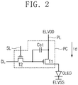
- FIG. 2 is an equivalent circuit diagram of one of the pixels constituting a display apparatus according to an embodiment of the present disclosure.
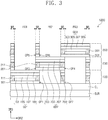
- the display region DA of the display apparatus 1000 may include a first pixel region PA1, a second pixel region PA2, a third pixel region PA3, and a plurality of margin regions MA.
- the first pixel PX1 may include a portion of the first light-emitting device module 100 and some elements of the circuit device layer CL, which are overlapped with the first pixel region PA1.
- Atomic components of chemical materials constituting the first non-emission layer 111 and the first light-emitting layer 105 may be substantially the same but their molecular structures may be different from each other.
- a material constituting the first non-emission layer 111 and a material constituting the first light-emitting layer 105 may include substantially the same atoms but may differ from each other in the bonding structure of the atoms.
- the molecular structure of the first non-emission layer 111 may be broken by short-wavelength light.
- a semiconductor pattern CSP of the transistor TFT may be located on the buffer layer BFL.
- a material for the semiconductor pattern CSP may be selected from amorphous silicon, polysilicon, or metal oxide semiconductor materials.
- a portion of the first pixel electrode 103 of the first light-emitting device OD1 may be overlapped with the margin region MA.
- a portion of the first pixel electrode 103 extended to the margin region MA may be exposed by the first pixel contact hole CK1.
- the first conductive layer MT1 may be formed by forming a seed layer on the exposed surface of the output electrode DE and performing a plating process to fill the first pixel contact hole CK1 with a conductive metal.
- the second pixel electrode 203 may be connected to the transistor TFT of the circuit device layer CL through a second pixel contact hole CK2 (see, for example, FIG. 1 ), and the third pixel electrode 303 may be connected to the transistor TFT of the circuit device layer CL through a third pixel contact hole CK3 (see, for example, FIG. 1 ), similar to the connection structure between the first pixel electrode 103 and the circuit device layer CL.
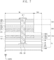
- FIG. 7 is a sectional view taken along the line III-III' of FIG. 1 .
- a connection structure between the first opposite electrode 107 of the first light-emitting device module 100 and the circuit device layer CL will be described with reference to FIG. 7 .
- the circuit device layer CL may include a power voltage pattern EVS.
- the power voltage pattern EVS may receive a constant reference voltage.
- FIG. 7 illustrates an example, in which the power voltage pattern EVS is located between the first insulating layer 10 and the second insulating layer 20, but the present disclosure is not limited to this example. For example, the position of the power voltage pattern EVS may be variously changed.
- a portion of the first opposite electrode 107 of the first light-emitting device OD1 may be overlapped with the margin region MA.
- a portion of the first opposite electrode 107 extended to the margin region MA may be exposed by the first opposite contact hole CB1.
- the second opposite electrode 207 and the third opposite electrode 307 may be overlapped with the margin region MA, and the second opposite electrode 207 and the third opposite electrode 307 may be partially exposed by the first opposite contact hole CB1.
- the second opposite electrode 207 and the third opposite electrode 307 may be electrically connected to the power voltage pattern EVS through the second conductive layer MT2.
- the second conductive layer MT2 may be formed by forming a seed layer on the exposed surface of the power voltage pattern EVS and performing a plating process to fill the first opposite contact hole CB1 with a conductive metal.
- the power voltage pattern EVS may be electrically connected to the first to third opposite electrodes 107, 207, and 307 through the first to third opposite contact holes CB1, CB2, and CB3, respectively.
- the present disclosure is not limited to this example, and in an embodiment, because the first to third opposite electrodes 107, 207, and 307 may receive the same voltage, one or more of the first to third opposite contact holes CB1, CB2, and CB3 may be omitted.
- the first light-emitting device module 100 may include a first substrate 131, a first light-emitting device OD11, and a first non-emission layer 141.
- the first light-emitting device OD11 may include a first pixel electrode 133, a first light-emitting layer 135, a first opposite electrode 137, and a first protection layer 139.
- a penetration hole may not be located in the first substrate 131 of the first light-emitting device module 100.
- the first substrate 131 may be overlapped with the first pixel region PA1, the second pixel region PA2, and the third pixel region PA3.
- the first light-emitting device OD11 may be located in the first pixel region PA1.
- the first opposite electrode 137 and the first protection layer 139 of the first light-emitting device module 100 may be overlapped with the second pixel region PA2 and the third pixel region PA3.
- the first non-emission layer 141 may be overlapped with not only the margin region MA but also the second and third pixel regions PA2 and PA3.
- the second light-emitting device module 200 may include a second substrate 231, a second light-emitting device OD21, and a second non-emission layer 241.
- the second light-emitting device OD21 may include a second pixel electrode 233, a second light-emitting layer 235, a second opposite electrode 237, and a second protection layer 239.
- a seventh penetration hole OP7 corresponding to the first pixel region PA1 may be provided in the second substrate 231.
- the second substrate 231 may be overlapped with the second pixel region PA2 and the third pixel region PA3.
- the second light-emitting device OD21 may be located in the second pixel region PA2.
- the second opposite electrode 237 and the second protection layer 239 of the second light-emitting device module 200 may be overlapped with the third pixel region PA3 but may not be overlapped with the first pixel region PA1.
- the second non-emission layer 241 may be overlapped with not only the margin region MA but also the third pixel region PA3.
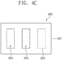
- the third light-emitting device module 300 may include a third substrate 331, a third light-emitting device OD31, and a third non-emission layer 341.
- the third light-emitting device OD31 may include a third pixel electrode 333, a third light-emitting layer 335, a third opposite electrode 337, and a third protection layer 339.
- An eighth penetration hole OP8 corresponding to the first pixel region PA1 and a ninth penetration hole OP9 corresponding to the second pixel region PA2 may be located in the third substrate 331.
- the third substrate 331 may be overlapped with the third pixel region PA3.
- the third light-emitting device OD31 may be located in the third pixel region PA3.
- the third opposite electrode 337 and the third protection layer 339 of the third light-emitting device module 300 may not be overlapped with the first pixel region PA1 and the second pixel region PA2.
- the third non-emission layer 341 may not be overlapped with the first pixel region PA1 and the second pixel region PA2.
- the display apparatus 1001 described with reference to FIG. 8 it may be possible to omit a process of forming a penetration hole in the first substrate 131 of the first light-emitting device module 100, compared with the display apparatus 1000 described with reference to FIG. 3 .
- the manufacturing process may be simplified, compared with the display apparatus 1000 of FIG. 3 .
- FIG. 9 is a plan view schematically illustrating a display apparatus according to another embodiment of the present disclosure.
- First to fourth pixels PX11, PX21, PX31, and PX41 emitting lights of different colors may be located in a display region DA of a display apparatus 1002.
- the first to fourth pixels PX11, PX21, PX31, and PX41 may emit red, green, blue, and white lights, respectively.
- the display apparatus 1000 of FIG. 3 may include three light-emitting device modules 100, 200, and 300, which are sequentially stacked, and the display apparatus 1002 of FIG. 9 may include four light-emitting device modules, which are sequentially stacked.
- the structure of the light-emitting device module may be substantially similar to each of the light-emitting device modules 100, 200, and 300 described with reference to FIG. 3 , and a detailed description may be omitted.
- FIG. 10 is a plan view illustrating an image information device according to an embodiment of the present disclosure.
- An image information device 2000 may include a plurality of display apparatuses 1100, 1200, 1300, and 1400.
- the plurality of display apparatuses 1100, 1200, 1300, and 1400 may be electrically connected to each other to output a single continuous image.
- Each of the display apparatuses 1100, 1200, 1300, and 1400 may include a display region DA1, which is used to display an image, and a peripheral region PRA, which is located outside the display region DA1.
- a structure of each of the display apparatuses 1100, 1200, 1300, and 1400 may be substantially similar to the display apparatus 1000 described with reference to FIGS. 1 - 7 , and a detailed description may be omitted.
- a driver, a power voltage supplying line, a pad, or the like may not be located in the peripheral region PRA, unlike the display apparatus 1000 of FIG. 1 . If the driver, the power voltage supplying line, and the pad are not located in the peripheral region PRA of the display apparatus 1100, a width of the peripheral region PRA may be substantially the same as a width of the margin region MA between pixels PX.
- a printed circuit board or a cable for receiving signals from the outside may be connected to at least one of the display apparatuses 1100, 1200, 1300, and 1400.
- a driver or the like may be located in the peripheral region PRA of at least one of the display apparatuses 1100, 1200, 1300, and 1400.
- the margin region(s) MA may have a relatively small width, compared with the comparative example, and thus, it may be possible to realize a high-resolution display apparatus. Furthermore, because a plurality of display apparatuses is electrically connected to each other, it may be possible to realize a high-resolution image information device 2000.
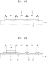
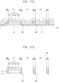
- FIGS. 11A - 11H are sectional views, which are taken along the line I-I' of FIG. 1 and illustrate a process of manufacturing the first light-emitting device module of the display apparatus shown in FIG. 1 .
- a support substrate SP may be prepared.
- a substrate 101 may be located on the support substrate SP.
- the substrate 101 may include silicon, glass, or plastic.
- a process of irradiating the first substrate 101 with a laser LZ is illustrated as an example of a method for forming the first penetration hole OP1 and the second penetration hole OP2.
- the present disclosure is not limited to this example, and the first penetration hole OP1 and the second penetration hole OP2 may be formed in the first substrate 101 using a dry etching process or a Bosch deep etching process.
- a first conductive layer EL1 may be formed on the first substrate 101.
- the first conductive layer EL1 may include iridium (Ir), chromium (Cr), or compounds thereof.
- the first conductive layer EL1 may include a plurality of layers.
- the first conductive layer EL1 may be a triple layered structure including ITO/Ag/ITO layers.
- a photosensitive film PR may be located on the first conductive layer EL1.
- the photosensitive film PR may be located on a region of the first conductive layer EL1 covering the first pixel region PA1.
- the first conductive layer EL1 may be patterned by a wet or dry etching process using the photosensitive film PR as an etch mask. Accordingly, the first pixel electrode 103 may be formed to be overlapped with the photosensitive film PR.
- the photosensitive film PR may be removed.
- a light-emitting pattern OLP may be formed on the first pixel electrode 103.
- the light-emitting pattern OLP may be formed by sequentially depositing a hole control layer, an organic light-emitting layer, and an electron control layer.
- a mask MSK may be placed over the light-emitting pattern OLP.
- the mask MSK may block light incident toward the first pixel region PA1 and may transmit light incident toward a region other than the first pixel region PA1.
- a first light SW may be irradiated onto the light-emitting pattern OLP through the mask MSK.
- the first light SW may be short-wavelength light or may have a wavelength of 300 nm or shorter.
- a portion of the light-emitting pattern OLP, which is overlapped with a region other than the first pixel region PA1, may be defined as the first non-emission layer 111, and the first light SW may result in damage to the first non-emission layer 111.
- the first light SW may cause breakage of a molecular structure (e.g., breakage in bonding structure of carbon molecules) constituting the portion of the light-emitting pattern OLP, which is overlapped with the region other than the first pixel region PA1.
- the portion of the light-emitting pattern OLP damaged by the first light SW may not emit light, even when electrons and holes are injected thereto.
- the first non-emission layer 111 may play the same role as the pixel definition layer in the display apparatus according to the comparative example. In an embodiment, because the first non-emission layer 111 is formed by the irradiation of the first light SW, it may not be necessary to form the pixel definition layer separately and this may make it possible to simplify a manufacturing process.
- a portion of the light-emitting pattern OLP, to which the first light SW is not irradiated, may be defined as the first light-emitting layer 105, and may emit light when voltages are applied to the first pixel electrode 103 and the first opposite electrode 107.
- the mask MSK is used to determine a region to be irradiated with the first light SW, it may be possible to control a size and a position of a light-emitting region (e.g., the first pixel region PA1) capable of effectively emitting light.
- a light-emitting region e.g., the first pixel region PA1
- the first opposite electrode 107 may be formed on the first light-emitting layer 105 and the first non-emission layer 111.
- the first opposite electrode 107 may include a conductive material having a low work function.
- the first opposite electrode 107 may include at least one of silver (Ag), magnesium (Mg), aluminum (Al), platinum (Pt), palladium (Pd), gold (Au), nickel (Ni), neodymium (Nd), iridium (Ir), chromium (Cr), lithium (Li), calcium (Ca), and alloys thereof.
- the first opposite electrode 107 may include at least one of aluminum (Al), silver (Ag), and magnesium-silver alloy (Mg:Ag).
- the first opposite electrode 107 may include an alloy, in which a content of silver (Ag) is higher than that of magnesium (Mg).
- the first opposite electrode 107 may be patterned in a manner similar to a process of forming the first pixel electrode 103 described with reference to FIGS. 11B - 11D . Thus, a detailed description of this process may be omitted.
- the first protection layer 109 may be formed on the first opposite electrode 107.
- the first protection layer 109 may include an insulating material. As a result, the process of manufacturing the first light-emitting device OD1 may be finished.
- the first substrate 101 may be separated from the support substrate SP. As a result, the fabrication of the first light-emitting device module 100 may be finished.
- the support substrate SP separated from the first substrate 101 may be discarded or may be cleaned and reused.
- a plurality of light-emitting device modules may be located at different levels, and this may make it possible to reduce a distance between light-emitting devices and to realize a high-resolution display apparatus.
- a short-wavelength light may be irradiated onto a light-emitting pattern, which is located on a remaining region other than a light-emitting region, and thus, it may be unnecessary to form a pixel definition layer separately. This may make it possible to simplify a manufacturing process.
Landscapes
- Engineering & Computer Science (AREA)
- Physics & Mathematics (AREA)
- Microelectronics & Electronic Packaging (AREA)
- Geometry (AREA)
- Optics & Photonics (AREA)
- Manufacturing & Machinery (AREA)
- Devices For Indicating Variable Information By Combining Individual Elements (AREA)
- Electroluminescent Light Sources (AREA)
Applications Claiming Priority (1)
| Application Number | Priority Date | Filing Date | Title |
|---|---|---|---|
| KR1020190006956A KR102676592B1 (ko) | 2019-01-18 | 2019-01-18 | 표시 장치 및 그 제조 방법 |
Publications (3)
| Publication Number | Publication Date |
|---|---|
| EP3683840A2 true EP3683840A2 (de) | 2020-07-22 |
| EP3683840A3 EP3683840A3 (de) | 2020-10-14 |
| EP3683840B1 EP3683840B1 (de) | 2023-05-03 |
Family
ID=69147504
Family Applications (1)
| Application Number | Title | Priority Date | Filing Date |
|---|---|---|---|
| EP20150643.3A Active EP3683840B1 (de) | 2019-01-18 | 2020-01-08 | Anzeigevorrichtung |
Country Status (4)
| Country | Link |
|---|---|
| US (1) | US11195880B2 (de) |
| EP (1) | EP3683840B1 (de) |
| KR (1) | KR102676592B1 (de) |
| CN (1) | CN111463237B (de) |
Family Cites Families (15)
| Publication number | Priority date | Publication date | Assignee | Title |
|---|---|---|---|---|
| US6368730B1 (en) * | 1997-10-13 | 2002-04-09 | Matsushita Electric Industrial Co., Ltd. | Electroluminescent device |
| KR100635056B1 (ko) | 2004-02-19 | 2006-10-16 | 삼성에스디아이 주식회사 | 유기전계 발광표시장치의 제조방법 |
| KR101821255B1 (ko) * | 2010-11-03 | 2018-01-24 | 삼성디스플레이 주식회사 | 유기 발광 표시 장치 |
| JP2012199231A (ja) * | 2011-03-04 | 2012-10-18 | Semiconductor Energy Lab Co Ltd | 表示装置 |
| CN103855193B (zh) * | 2014-03-05 | 2017-02-08 | 京东方科技集团股份有限公司 | 一种oled显示面板及其制备方法、显示装置 |
| KR102500271B1 (ko) * | 2015-08-19 | 2023-02-16 | 삼성디스플레이 주식회사 | 유기 발광 표시 장치 및 유기 발광 표시 장치의 제조 방법 |
| KR102406606B1 (ko) * | 2015-10-08 | 2022-06-09 | 삼성디스플레이 주식회사 | 유기 발광 소자, 이를 포함하는 유기 발광 표시 장치, 및 이의 제조 방법 |
| KR102378976B1 (ko) * | 2016-05-18 | 2022-03-24 | 가부시키가이샤 한도오따이 에네루기 켄큐쇼 | 박리 방법, 표시 장치, 모듈, 및 전자 기기 |
| WO2017209437A1 (en) | 2016-05-31 | 2017-12-07 | Lg Electronics Inc. | Display device using semiconductor light emitting device and fabrication method thereof |
| KR101968527B1 (ko) | 2016-05-31 | 2019-04-12 | 엘지전자 주식회사 | 반도체 발광 소자를 이용한 디스플레이 장치 및 이의 제조방법 |
| TWI704671B (zh) * | 2016-06-24 | 2020-09-11 | 日商半導體能源研究所股份有限公司 | 顯示裝置以及其驅動方法 |
| KR102611794B1 (ko) | 2016-11-30 | 2023-12-07 | 엘지디스플레이 주식회사 | 유기발광 표시장치와 그의 제조방법 |
| JP2018142442A (ja) * | 2017-02-27 | 2018-09-13 | 株式会社ジャパンディスプレイ | 有機el表示装置の製造方法及び有機el表示装置 |
| JP7261220B2 (ja) * | 2018-03-06 | 2023-04-19 | ソニーセミコンダクタソリューションズ株式会社 | 表示デバイス |
| TWI692865B (zh) * | 2018-11-21 | 2020-05-01 | 友達光電股份有限公司 | 顯示裝置 |
-
2019
- 2019-01-18 KR KR1020190006956A patent/KR102676592B1/ko active Active
-
2020
- 2020-01-08 EP EP20150643.3A patent/EP3683840B1/de active Active
- 2020-01-09 CN CN202010020772.7A patent/CN111463237B/zh active Active
- 2020-01-15 US US16/744,106 patent/US11195880B2/en active Active
Also Published As
| Publication number | Publication date |
|---|---|
| US20200235170A1 (en) | 2020-07-23 |
| KR20200090300A (ko) | 2020-07-29 |
| KR102676592B1 (ko) | 2024-06-21 |
| CN111463237A (zh) | 2020-07-28 |
| CN111463237B (zh) | 2025-06-10 |
| US11195880B2 (en) | 2021-12-07 |
| EP3683840A3 (de) | 2020-10-14 |
| EP3683840B1 (de) | 2023-05-03 |
Similar Documents
| Publication | Publication Date | Title |
|---|---|---|
| US10840478B2 (en) | Display panel | |
| US11107869B2 (en) | Display device | |
| KR102652822B1 (ko) | 전계 발광 표시 장치 | |
| CN106057847B (zh) | 显示面板 | |
| US10033017B2 (en) | Organic light emitting display device and method of manufacturing the same | |
| US11450268B2 (en) | Display device and fabricating method for display device | |
| US12082469B2 (en) | Display apparatus and method of manufacturing the same | |
| US11063030B2 (en) | Display device and method of fabricating the same | |
| US11730026B2 (en) | Display apparatus | |
| US20240049508A1 (en) | Display device and method of manufacturing the same | |
| EP3683840B1 (de) | Anzeigevorrichtung | |
| CN114628440A (zh) | 显示设备及其制造方法 | |
| US20240023378A1 (en) | Display device | |
| US20240016034A1 (en) | Display device and method of manufacturing the same | |
| US20230389398A1 (en) | Display panel and display device | |
| US20250024720A1 (en) | Display device and method of providing the same | |
| CN221151905U (zh) | 显示装置 | |
| US12457858B2 (en) | Display device | |
| US20240324314A1 (en) | Display apparatus | |
| US20250063916A1 (en) | Display device | |
| KR102926292B1 (ko) | 표시 장치 및 표시 장치의 제조 방법 | |
| US20220328612A1 (en) | Display device | |
| CN118475181A (zh) | 显示设备和制造显示设备的方法 | |
| KR20250027478A (ko) | 표시 장치 |
Legal Events
| Date | Code | Title | Description |
|---|---|---|---|
| PUAI | Public reference made under article 153(3) epc to a published international application that has entered the european phase |
Free format text: ORIGINAL CODE: 0009012 |
|
| STAA | Information on the status of an ep patent application or granted ep patent |
Free format text: STATUS: THE APPLICATION HAS BEEN PUBLISHED |
|
| AK | Designated contracting states |
Kind code of ref document: A2 Designated state(s): AL AT BE BG CH CY CZ DE DK EE ES FI FR GB GR HR HU IE IS IT LI LT LU LV MC MK MT NL NO PL PT RO RS SE SI SK SM TR |
|
| AX | Request for extension of the european patent |
Extension state: BA ME |
|
| PUAL | Search report despatched |
Free format text: ORIGINAL CODE: 0009013 |
|
| AK | Designated contracting states |
Kind code of ref document: A3 Designated state(s): AL AT BE BG CH CY CZ DE DK EE ES FI FR GB GR HR HU IE IS IT LI LT LU LV MC MK MT NL NO PL PT RO RS SE SI SK SM TR |
|
| AX | Request for extension of the european patent |
Extension state: BA ME |
|
| RIC1 | Information provided on ipc code assigned before grant |
Ipc: H01L 25/04 20140101ALI20200910BHEP Ipc: H01L 27/32 20060101AFI20200910BHEP |
|
| STAA | Information on the status of an ep patent application or granted ep patent |
Free format text: STATUS: REQUEST FOR EXAMINATION WAS MADE |
|
| 17P | Request for examination filed |
Effective date: 20210407 |
|
| RBV | Designated contracting states (corrected) |
Designated state(s): AL AT BE BG CH CY CZ DE DK EE ES FI FR GB GR HR HU IE IS IT LI LT LU LV MC MK MT NL NO PL PT RO RS SE SI SK SM TR |
|
| STAA | Information on the status of an ep patent application or granted ep patent |
Free format text: STATUS: EXAMINATION IS IN PROGRESS |
|
| 17Q | First examination report despatched |
Effective date: 20210805 |
|
| GRAP | Despatch of communication of intention to grant a patent |
Free format text: ORIGINAL CODE: EPIDOSNIGR1 |
|
| STAA | Information on the status of an ep patent application or granted ep patent |
Free format text: STATUS: GRANT OF PATENT IS INTENDED |
|
| INTG | Intention to grant announced |
Effective date: 20221207 |
|
| GRAS | Grant fee paid |
Free format text: ORIGINAL CODE: EPIDOSNIGR3 |
|
| GRAA | (expected) grant |
Free format text: ORIGINAL CODE: 0009210 |
|
| STAA | Information on the status of an ep patent application or granted ep patent |
Free format text: STATUS: THE PATENT HAS BEEN GRANTED |
|
| AK | Designated contracting states |
Kind code of ref document: B1 Designated state(s): AL AT BE BG CH CY CZ DE DK EE ES FI FR GB GR HR HU IE IS IT LI LT LU LV MC MK MT NL NO PL PT RO RS SE SI SK SM TR |
|
| REG | Reference to a national code |
Ref country code: GB Ref legal event code: FG4D |
|
| REG | Reference to a national code |
Ref country code: AT Ref legal event code: REF Ref document number: 1565403 Country of ref document: AT Kind code of ref document: T Effective date: 20230515 Ref country code: CH Ref legal event code: EP |
|
| REG | Reference to a national code |
Ref country code: DE Ref legal event code: R096 Ref document number: 602020010219 Country of ref document: DE |
|
| REG | Reference to a national code |
Ref country code: IE Ref legal event code: FG4D |
|
| P01 | Opt-out of the competence of the unified patent court (upc) registered |
Effective date: 20230516 |
|
| REG | Reference to a national code |
Ref country code: NL Ref legal event code: FP |
|
| REG | Reference to a national code |
Ref country code: LT Ref legal event code: MG9D |
|
| REG | Reference to a national code |
Ref country code: AT Ref legal event code: MK05 Ref document number: 1565403 Country of ref document: AT Kind code of ref document: T Effective date: 20230503 |
|
| PG25 | Lapsed in a contracting state [announced via postgrant information from national office to epo] |
Ref country code: SE Free format text: LAPSE BECAUSE OF FAILURE TO SUBMIT A TRANSLATION OF THE DESCRIPTION OR TO PAY THE FEE WITHIN THE PRESCRIBED TIME-LIMIT Effective date: 20230503 Ref country code: PT Free format text: LAPSE BECAUSE OF FAILURE TO SUBMIT A TRANSLATION OF THE DESCRIPTION OR TO PAY THE FEE WITHIN THE PRESCRIBED TIME-LIMIT Effective date: 20230904 Ref country code: NO Free format text: LAPSE BECAUSE OF FAILURE TO SUBMIT A TRANSLATION OF THE DESCRIPTION OR TO PAY THE FEE WITHIN THE PRESCRIBED TIME-LIMIT Effective date: 20230803 Ref country code: ES Free format text: LAPSE BECAUSE OF FAILURE TO SUBMIT A TRANSLATION OF THE DESCRIPTION OR TO PAY THE FEE WITHIN THE PRESCRIBED TIME-LIMIT Effective date: 20230503 Ref country code: AT Free format text: LAPSE BECAUSE OF FAILURE TO SUBMIT A TRANSLATION OF THE DESCRIPTION OR TO PAY THE FEE WITHIN THE PRESCRIBED TIME-LIMIT Effective date: 20230503 |
|
| PG25 | Lapsed in a contracting state [announced via postgrant information from national office to epo] |
Ref country code: RS Free format text: LAPSE BECAUSE OF FAILURE TO SUBMIT A TRANSLATION OF THE DESCRIPTION OR TO PAY THE FEE WITHIN THE PRESCRIBED TIME-LIMIT Effective date: 20230503 Ref country code: PL Free format text: LAPSE BECAUSE OF FAILURE TO SUBMIT A TRANSLATION OF THE DESCRIPTION OR TO PAY THE FEE WITHIN THE PRESCRIBED TIME-LIMIT Effective date: 20230503 Ref country code: LV Free format text: LAPSE BECAUSE OF FAILURE TO SUBMIT A TRANSLATION OF THE DESCRIPTION OR TO PAY THE FEE WITHIN THE PRESCRIBED TIME-LIMIT Effective date: 20230503 Ref country code: LT Free format text: LAPSE BECAUSE OF FAILURE TO SUBMIT A TRANSLATION OF THE DESCRIPTION OR TO PAY THE FEE WITHIN THE PRESCRIBED TIME-LIMIT Effective date: 20230503 Ref country code: IS Free format text: LAPSE BECAUSE OF FAILURE TO SUBMIT A TRANSLATION OF THE DESCRIPTION OR TO PAY THE FEE WITHIN THE PRESCRIBED TIME-LIMIT Effective date: 20230903 Ref country code: HR Free format text: LAPSE BECAUSE OF FAILURE TO SUBMIT A TRANSLATION OF THE DESCRIPTION OR TO PAY THE FEE WITHIN THE PRESCRIBED TIME-LIMIT Effective date: 20230503 Ref country code: GR Free format text: LAPSE BECAUSE OF FAILURE TO SUBMIT A TRANSLATION OF THE DESCRIPTION OR TO PAY THE FEE WITHIN THE PRESCRIBED TIME-LIMIT Effective date: 20230804 |
|
| PG25 | Lapsed in a contracting state [announced via postgrant information from national office to epo] |
Ref country code: FI Free format text: LAPSE BECAUSE OF FAILURE TO SUBMIT A TRANSLATION OF THE DESCRIPTION OR TO PAY THE FEE WITHIN THE PRESCRIBED TIME-LIMIT Effective date: 20230503 |
|
| PG25 | Lapsed in a contracting state [announced via postgrant information from national office to epo] |
Ref country code: SK Free format text: LAPSE BECAUSE OF FAILURE TO SUBMIT A TRANSLATION OF THE DESCRIPTION OR TO PAY THE FEE WITHIN THE PRESCRIBED TIME-LIMIT Effective date: 20230503 |
|
| PG25 | Lapsed in a contracting state [announced via postgrant information from national office to epo] |
Ref country code: SM Free format text: LAPSE BECAUSE OF FAILURE TO SUBMIT A TRANSLATION OF THE DESCRIPTION OR TO PAY THE FEE WITHIN THE PRESCRIBED TIME-LIMIT Effective date: 20230503 Ref country code: SK Free format text: LAPSE BECAUSE OF FAILURE TO SUBMIT A TRANSLATION OF THE DESCRIPTION OR TO PAY THE FEE WITHIN THE PRESCRIBED TIME-LIMIT Effective date: 20230503 Ref country code: RO Free format text: LAPSE BECAUSE OF FAILURE TO SUBMIT A TRANSLATION OF THE DESCRIPTION OR TO PAY THE FEE WITHIN THE PRESCRIBED TIME-LIMIT Effective date: 20230503 Ref country code: EE Free format text: LAPSE BECAUSE OF FAILURE TO SUBMIT A TRANSLATION OF THE DESCRIPTION OR TO PAY THE FEE WITHIN THE PRESCRIBED TIME-LIMIT Effective date: 20230503 Ref country code: DK Free format text: LAPSE BECAUSE OF FAILURE TO SUBMIT A TRANSLATION OF THE DESCRIPTION OR TO PAY THE FEE WITHIN THE PRESCRIBED TIME-LIMIT Effective date: 20230503 Ref country code: CZ Free format text: LAPSE BECAUSE OF FAILURE TO SUBMIT A TRANSLATION OF THE DESCRIPTION OR TO PAY THE FEE WITHIN THE PRESCRIBED TIME-LIMIT Effective date: 20230503 |
|
| REG | Reference to a national code |
Ref country code: DE Ref legal event code: R097 Ref document number: 602020010219 Country of ref document: DE |
|
| PLBE | No opposition filed within time limit |
Free format text: ORIGINAL CODE: 0009261 |
|
| STAA | Information on the status of an ep patent application or granted ep patent |
Free format text: STATUS: NO OPPOSITION FILED WITHIN TIME LIMIT |
|
| 26N | No opposition filed |
Effective date: 20240206 |
|
| PG25 | Lapsed in a contracting state [announced via postgrant information from national office to epo] |
Ref country code: SI Free format text: LAPSE BECAUSE OF FAILURE TO SUBMIT A TRANSLATION OF THE DESCRIPTION OR TO PAY THE FEE WITHIN THE PRESCRIBED TIME-LIMIT Effective date: 20230503 |
|
| PG25 | Lapsed in a contracting state [announced via postgrant information from national office to epo] |
Ref country code: SI Free format text: LAPSE BECAUSE OF FAILURE TO SUBMIT A TRANSLATION OF THE DESCRIPTION OR TO PAY THE FEE WITHIN THE PRESCRIBED TIME-LIMIT Effective date: 20230503 Ref country code: IT Free format text: LAPSE BECAUSE OF FAILURE TO SUBMIT A TRANSLATION OF THE DESCRIPTION OR TO PAY THE FEE WITHIN THE PRESCRIBED TIME-LIMIT Effective date: 20230503 |
|
| PG25 | Lapsed in a contracting state [announced via postgrant information from national office to epo] |
Ref country code: MC Free format text: LAPSE BECAUSE OF FAILURE TO SUBMIT A TRANSLATION OF THE DESCRIPTION OR TO PAY THE FEE WITHIN THE PRESCRIBED TIME-LIMIT Effective date: 20230503 |
|
| PG25 | Lapsed in a contracting state [announced via postgrant information from national office to epo] |
Ref country code: MC Free format text: LAPSE BECAUSE OF FAILURE TO SUBMIT A TRANSLATION OF THE DESCRIPTION OR TO PAY THE FEE WITHIN THE PRESCRIBED TIME-LIMIT Effective date: 20230503 |
|
| REG | Reference to a national code |
Ref country code: CH Ref legal event code: PL |
|
| PG25 | Lapsed in a contracting state [announced via postgrant information from national office to epo] |
Ref country code: LU Free format text: LAPSE BECAUSE OF NON-PAYMENT OF DUE FEES Effective date: 20240108 |
|
| PG25 | Lapsed in a contracting state [announced via postgrant information from national office to epo] |
Ref country code: LU Free format text: LAPSE BECAUSE OF NON-PAYMENT OF DUE FEES Effective date: 20240108 |
|
| PG25 | Lapsed in a contracting state [announced via postgrant information from national office to epo] |
Ref country code: BE Free format text: LAPSE BECAUSE OF NON-PAYMENT OF DUE FEES Effective date: 20240131 |
|
| PG25 | Lapsed in a contracting state [announced via postgrant information from national office to epo] |
Ref country code: CH Free format text: LAPSE BECAUSE OF NON-PAYMENT OF DUE FEES Effective date: 20240131 |
|
| PG25 | Lapsed in a contracting state [announced via postgrant information from national office to epo] |
Ref country code: CH Free format text: LAPSE BECAUSE OF NON-PAYMENT OF DUE FEES Effective date: 20240131 Ref country code: BE Free format text: LAPSE BECAUSE OF NON-PAYMENT OF DUE FEES Effective date: 20240131 |
|
| REG | Reference to a national code |
Ref country code: BE Ref legal event code: MM Effective date: 20240131 |
|
| PG25 | Lapsed in a contracting state [announced via postgrant information from national office to epo] |
Ref country code: BG Free format text: LAPSE BECAUSE OF FAILURE TO SUBMIT A TRANSLATION OF THE DESCRIPTION OR TO PAY THE FEE WITHIN THE PRESCRIBED TIME-LIMIT Effective date: 20230503 |
|
| PG25 | Lapsed in a contracting state [announced via postgrant information from national office to epo] |
Ref country code: BG Free format text: LAPSE BECAUSE OF FAILURE TO SUBMIT A TRANSLATION OF THE DESCRIPTION OR TO PAY THE FEE WITHIN THE PRESCRIBED TIME-LIMIT Effective date: 20230503 |
|
| PG25 | Lapsed in a contracting state [announced via postgrant information from national office to epo] |
Ref country code: IE Free format text: LAPSE BECAUSE OF NON-PAYMENT OF DUE FEES Effective date: 20240108 |
|
| PG25 | Lapsed in a contracting state [announced via postgrant information from national office to epo] |
Ref country code: IE Free format text: LAPSE BECAUSE OF NON-PAYMENT OF DUE FEES Effective date: 20240108 |
|
| PG25 | Lapsed in a contracting state [announced via postgrant information from national office to epo] |
Ref country code: CY Free format text: LAPSE BECAUSE OF FAILURE TO SUBMIT A TRANSLATION OF THE DESCRIPTION OR TO PAY THE FEE WITHIN THE PRESCRIBED TIME-LIMIT; INVALID AB INITIO Effective date: 20200108 |
|
| PG25 | Lapsed in a contracting state [announced via postgrant information from national office to epo] |
Ref country code: HU Free format text: LAPSE BECAUSE OF FAILURE TO SUBMIT A TRANSLATION OF THE DESCRIPTION OR TO PAY THE FEE WITHIN THE PRESCRIBED TIME-LIMIT; INVALID AB INITIO Effective date: 20200108 |
|
| PG25 | Lapsed in a contracting state [announced via postgrant information from national office to epo] |
Ref country code: TR Free format text: LAPSE BECAUSE OF FAILURE TO SUBMIT A TRANSLATION OF THE DESCRIPTION OR TO PAY THE FEE WITHIN THE PRESCRIBED TIME-LIMIT Effective date: 20230503 |
|
| PGFP | Annual fee paid to national office [announced via postgrant information from national office to epo] |
Ref country code: GB Payment date: 20251222 Year of fee payment: 7 |
|
| PGFP | Annual fee paid to national office [announced via postgrant information from national office to epo] |
Ref country code: FR Payment date: 20251223 Year of fee payment: 7 Ref country code: NL Payment date: 20251223 Year of fee payment: 7 |
|
| PGFP | Annual fee paid to national office [announced via postgrant information from national office to epo] |
Ref country code: DE Payment date: 20251222 Year of fee payment: 7 |