EP3680948B1 - Organic light-emitting device - Google Patents
Organic light-emitting device Download PDFInfo
- Publication number
- EP3680948B1 EP3680948B1 EP20155229.6A EP20155229A EP3680948B1 EP 3680948 B1 EP3680948 B1 EP 3680948B1 EP 20155229 A EP20155229 A EP 20155229A EP 3680948 B1 EP3680948 B1 EP 3680948B1
- Authority
- EP
- European Patent Office
- Prior art keywords
- group
- unsubstituted
- substituted
- salt
- formulae
- Prior art date
- Legal status (The legal status is an assumption and is not a legal conclusion. Google has not performed a legal analysis and makes no representation as to the accuracy of the status listed.)
- Active
Links
Images
Classifications
-
- H—ELECTRICITY
- H10—SEMICONDUCTOR DEVICES; ELECTRIC SOLID-STATE DEVICES NOT OTHERWISE PROVIDED FOR
- H10K—ORGANIC ELECTRIC SOLID-STATE DEVICES
- H10K85/00—Organic materials used in the body or electrodes of devices covered by this subclass
- H10K85/60—Organic compounds having low molecular weight
- H10K85/649—Aromatic compounds comprising a hetero atom
- H10K85/657—Polycyclic condensed heteroaromatic hydrocarbons
- H10K85/6572—Polycyclic condensed heteroaromatic hydrocarbons comprising only nitrogen in the heteroaromatic polycondensed ring system, e.g. phenanthroline or carbazole
-
- C—CHEMISTRY; METALLURGY
- C09—DYES; PAINTS; POLISHES; NATURAL RESINS; ADHESIVES; COMPOSITIONS NOT OTHERWISE PROVIDED FOR; APPLICATIONS OF MATERIALS NOT OTHERWISE PROVIDED FOR
- C09K—MATERIALS FOR MISCELLANEOUS APPLICATIONS, NOT PROVIDED FOR ELSEWHERE
- C09K11/00—Luminescent, e.g. electroluminescent, chemiluminescent materials
- C09K11/02—Use of particular materials as binders, particle coatings or suspension media therefor
- C09K11/025—Use of particular materials as binders, particle coatings or suspension media therefor non-luminescent particle coatings or suspension media
-
- C—CHEMISTRY; METALLURGY
- C09—DYES; PAINTS; POLISHES; NATURAL RESINS; ADHESIVES; COMPOSITIONS NOT OTHERWISE PROVIDED FOR; APPLICATIONS OF MATERIALS NOT OTHERWISE PROVIDED FOR
- C09K—MATERIALS FOR MISCELLANEOUS APPLICATIONS, NOT PROVIDED FOR ELSEWHERE
- C09K11/00—Luminescent, e.g. electroluminescent, chemiluminescent materials
- C09K11/06—Luminescent, e.g. electroluminescent, chemiluminescent materials containing organic luminescent materials
-
- H—ELECTRICITY
- H10—SEMICONDUCTOR DEVICES; ELECTRIC SOLID-STATE DEVICES NOT OTHERWISE PROVIDED FOR
- H10K—ORGANIC ELECTRIC SOLID-STATE DEVICES
- H10K50/00—Organic light-emitting devices
- H10K50/10—OLEDs or polymer light-emitting diodes [PLED]
- H10K50/11—OLEDs or polymer light-emitting diodes [PLED] characterised by the electroluminescent [EL] layers
- H10K50/12—OLEDs or polymer light-emitting diodes [PLED] characterised by the electroluminescent [EL] layers comprising dopants
-
- H—ELECTRICITY
- H10—SEMICONDUCTOR DEVICES; ELECTRIC SOLID-STATE DEVICES NOT OTHERWISE PROVIDED FOR
- H10K—ORGANIC ELECTRIC SOLID-STATE DEVICES
- H10K50/00—Organic light-emitting devices
- H10K50/10—OLEDs or polymer light-emitting diodes [PLED]
- H10K50/14—Carrier transporting layers
- H10K50/15—Hole transporting layers
-
- H—ELECTRICITY
- H10—SEMICONDUCTOR DEVICES; ELECTRIC SOLID-STATE DEVICES NOT OTHERWISE PROVIDED FOR
- H10K—ORGANIC ELECTRIC SOLID-STATE DEVICES
- H10K50/00—Organic light-emitting devices
- H10K50/10—OLEDs or polymer light-emitting diodes [PLED]
- H10K50/14—Carrier transporting layers
- H10K50/16—Electron transporting layers
-
- H—ELECTRICITY
- H10—SEMICONDUCTOR DEVICES; ELECTRIC SOLID-STATE DEVICES NOT OTHERWISE PROVIDED FOR
- H10K—ORGANIC ELECTRIC SOLID-STATE DEVICES
- H10K50/00—Organic light-emitting devices
- H10K50/10—OLEDs or polymer light-emitting diodes [PLED]
- H10K50/17—Carrier injection layers
-
- H—ELECTRICITY
- H10—SEMICONDUCTOR DEVICES; ELECTRIC SOLID-STATE DEVICES NOT OTHERWISE PROVIDED FOR
- H10K—ORGANIC ELECTRIC SOLID-STATE DEVICES
- H10K50/00—Organic light-emitting devices
- H10K50/80—Constructional details
-
- H—ELECTRICITY
- H10—SEMICONDUCTOR DEVICES; ELECTRIC SOLID-STATE DEVICES NOT OTHERWISE PROVIDED FOR
- H10K—ORGANIC ELECTRIC SOLID-STATE DEVICES
- H10K50/00—Organic light-emitting devices
- H10K50/80—Constructional details
- H10K50/85—Arrangements for extracting light from the devices
- H10K50/856—Arrangements for extracting light from the devices comprising reflective means
-
- H—ELECTRICITY
- H10—SEMICONDUCTOR DEVICES; ELECTRIC SOLID-STATE DEVICES NOT OTHERWISE PROVIDED FOR
- H10K—ORGANIC ELECTRIC SOLID-STATE DEVICES
- H10K59/00—Integrated devices, or assemblies of multiple devices, comprising at least one organic light-emitting element covered by group H10K50/00
- H10K59/80—Constructional details
-
- H—ELECTRICITY
- H10—SEMICONDUCTOR DEVICES; ELECTRIC SOLID-STATE DEVICES NOT OTHERWISE PROVIDED FOR
- H10K—ORGANIC ELECTRIC SOLID-STATE DEVICES
- H10K85/00—Organic materials used in the body or electrodes of devices covered by this subclass
- H10K85/30—Coordination compounds
- H10K85/341—Transition metal complexes, e.g. Ru(II)polypyridine complexes
- H10K85/342—Transition metal complexes, e.g. Ru(II)polypyridine complexes comprising iridium
-
- H—ELECTRICITY
- H10—SEMICONDUCTOR DEVICES; ELECTRIC SOLID-STATE DEVICES NOT OTHERWISE PROVIDED FOR
- H10K—ORGANIC ELECTRIC SOLID-STATE DEVICES
- H10K85/00—Organic materials used in the body or electrodes of devices covered by this subclass
- H10K85/60—Organic compounds having low molecular weight
- H10K85/615—Polycyclic condensed aromatic hydrocarbons, e.g. anthracene
- H10K85/622—Polycyclic condensed aromatic hydrocarbons, e.g. anthracene containing four rings, e.g. pyrene
-
- H—ELECTRICITY
- H10—SEMICONDUCTOR DEVICES; ELECTRIC SOLID-STATE DEVICES NOT OTHERWISE PROVIDED FOR
- H10K—ORGANIC ELECTRIC SOLID-STATE DEVICES
- H10K85/00—Organic materials used in the body or electrodes of devices covered by this subclass
- H10K85/60—Organic compounds having low molecular weight
- H10K85/631—Amine compounds having at least two aryl rest on at least one amine-nitrogen atom, e.g. triphenylamine
- H10K85/633—Amine compounds having at least two aryl rest on at least one amine-nitrogen atom, e.g. triphenylamine comprising polycyclic condensed aromatic hydrocarbons as substituents on the nitrogen atom
-
- H—ELECTRICITY
- H10—SEMICONDUCTOR DEVICES; ELECTRIC SOLID-STATE DEVICES NOT OTHERWISE PROVIDED FOR
- H10K—ORGANIC ELECTRIC SOLID-STATE DEVICES
- H10K85/00—Organic materials used in the body or electrodes of devices covered by this subclass
- H10K85/60—Organic compounds having low molecular weight
- H10K85/631—Amine compounds having at least two aryl rest on at least one amine-nitrogen atom, e.g. triphenylamine
- H10K85/636—Amine compounds having at least two aryl rest on at least one amine-nitrogen atom, e.g. triphenylamine comprising heteroaromatic hydrocarbons as substituents on the nitrogen atom
-
- H—ELECTRICITY
- H10—SEMICONDUCTOR DEVICES; ELECTRIC SOLID-STATE DEVICES NOT OTHERWISE PROVIDED FOR
- H10K—ORGANIC ELECTRIC SOLID-STATE DEVICES
- H10K85/00—Organic materials used in the body or electrodes of devices covered by this subclass
- H10K85/60—Organic compounds having low molecular weight
- H10K85/649—Aromatic compounds comprising a hetero atom
- H10K85/654—Aromatic compounds comprising a hetero atom comprising only nitrogen as heteroatom
-
- H—ELECTRICITY
- H10—SEMICONDUCTOR DEVICES; ELECTRIC SOLID-STATE DEVICES NOT OTHERWISE PROVIDED FOR
- H10K—ORGANIC ELECTRIC SOLID-STATE DEVICES
- H10K85/00—Organic materials used in the body or electrodes of devices covered by this subclass
- H10K85/60—Organic compounds having low molecular weight
- H10K85/649—Aromatic compounds comprising a hetero atom
- H10K85/657—Polycyclic condensed heteroaromatic hydrocarbons
- H10K85/6574—Polycyclic condensed heteroaromatic hydrocarbons comprising only oxygen in the heteroaromatic polycondensed ring system, e.g. cumarine dyes
-
- C—CHEMISTRY; METALLURGY
- C09—DYES; PAINTS; POLISHES; NATURAL RESINS; ADHESIVES; COMPOSITIONS NOT OTHERWISE PROVIDED FOR; APPLICATIONS OF MATERIALS NOT OTHERWISE PROVIDED FOR
- C09K—MATERIALS FOR MISCELLANEOUS APPLICATIONS, NOT PROVIDED FOR ELSEWHERE
- C09K2211/00—Chemical nature of organic luminescent or tenebrescent compounds
- C09K2211/18—Metal complexes
- C09K2211/185—Metal complexes of the platinum group, i.e. Os, Ir, Pt, Ru, Rh or Pd
-
- H—ELECTRICITY
- H10—SEMICONDUCTOR DEVICES; ELECTRIC SOLID-STATE DEVICES NOT OTHERWISE PROVIDED FOR
- H10K—ORGANIC ELECTRIC SOLID-STATE DEVICES
- H10K2101/00—Properties of the organic materials covered by group H10K85/00
- H10K2101/10—Triplet emission
-
- H—ELECTRICITY
- H10—SEMICONDUCTOR DEVICES; ELECTRIC SOLID-STATE DEVICES NOT OTHERWISE PROVIDED FOR
- H10K—ORGANIC ELECTRIC SOLID-STATE DEVICES
- H10K2102/00—Constructional details relating to the organic devices covered by this subclass
- H10K2102/301—Details of OLEDs
-
- H—ELECTRICITY
- H10—SEMICONDUCTOR DEVICES; ELECTRIC SOLID-STATE DEVICES NOT OTHERWISE PROVIDED FOR
- H10K—ORGANIC ELECTRIC SOLID-STATE DEVICES
- H10K50/00—Organic light-emitting devices
- H10K50/10—OLEDs or polymer light-emitting diodes [PLED]
- H10K50/11—OLEDs or polymer light-emitting diodes [PLED] characterised by the electroluminescent [EL] layers
-
- H—ELECTRICITY
- H10—SEMICONDUCTOR DEVICES; ELECTRIC SOLID-STATE DEVICES NOT OTHERWISE PROVIDED FOR
- H10K—ORGANIC ELECTRIC SOLID-STATE DEVICES
- H10K50/00—Organic light-emitting devices
- H10K50/10—OLEDs or polymer light-emitting diodes [PLED]
- H10K50/17—Carrier injection layers
- H10K50/171—Electron injection layers
-
- H—ELECTRICITY
- H10—SEMICONDUCTOR DEVICES; ELECTRIC SOLID-STATE DEVICES NOT OTHERWISE PROVIDED FOR
- H10K—ORGANIC ELECTRIC SOLID-STATE DEVICES
- H10K85/00—Organic materials used in the body or electrodes of devices covered by this subclass
- H10K85/60—Organic compounds having low molecular weight
- H10K85/615—Polycyclic condensed aromatic hydrocarbons, e.g. anthracene
- H10K85/626—Polycyclic condensed aromatic hydrocarbons, e.g. anthracene containing more than one polycyclic condensed aromatic rings, e.g. bis-anthracene
Definitions
- the present invention relates to an organic light-emitting device.
- OLEDs Organic light-emitting devices
- OLEDs are self-emission devices that have wide viewing angles, high contrast ratios, and short response times.
- the OLEDs exhibit excellent luminance, driving voltage, and response speed characteristics.
- An OLED may comprise a first electrode disposed (e.g., positioned) on a substrate, and a hole transport region, an emission layer, an electron transport region, and a second electrode, which are sequentially disposed on the first electrode. Holes provided from the first electrode may move toward the emission layer through the hole transport region, and electrons provided from the second electrode may move toward the emission layer through the electron transport region. The holes and the electrons may then recombine in the emission layer to produce excitons. These excitons change from an excited state to a ground state to thereby generate light.
- the present invention provides an organic light-emitting device having low driving voltage, high efficiency, and long lifespan.
- the present invention provides an organic light-emitting device as set out in the claims.
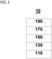
- Figure 1 illustrates a schematic view of an organic light-emitting device according to an embodiment of the present invention.
- the term “and/or” includes any and all combinations of one or more of the associated listed items. Expressions such as “at least one of,” “one of,” “at least one selected from,” and “one selected from,” when preceding a list of elements, modify the entire list of elements and do not modify the individual elements of the list. Further, the use of “may” when describing embodiments of the present invention refers to “one or more embodiments of the present invention.”
- the organic light-emitting device of the present invention comprises: a first electrode; a second electrode facing the first electrode; a first layer between the first electrode and the second electrode and comprising a first compound; a second layer between the first layer and the second electrode and comprising a second compound; and a third layer between the second layer and the second electrode and comprising a third compound.
- the first electrode may be an anode.
- the second electrode may be a cathode. Descriptions of the first electrode and the second electrode are as provided herein.
- * indicates a binding site to an adjacent atom.
- a group represented by Formula A may be a group represented by Formula A(1) or A(2).
- a group represented by Formula B may be a group represented by one of Formulae B(1) to B(4).
- a group represented by Formula C may be a group represented by one of Formulae C(1) to C(16).
- the first compound, the second compound, and the third compound may each independently comprise at least one group represented by Formulae A(1), A(2), B(1) to B(4), and C(1) to C(16): wherein, in Formulae A(1), A(2), B(1) to B(4), and C(1) to C(16),
- ring A 1 , ring A 11 , and ring A 12 may each independently be selected from a C 3 -C 30 carbocyclic group and a C 2 -C 30 heterocyclic group, and R 1 , R 2 , R 11 , and R 12 may each independently be selected from:
- R 1a to R 1a , R 2a , R 2b , R 11a to R 11b , and R 12a to R 12d may be each independently selected from:
- L 25 may be selected from a substituted or unsubstituted C 3 -C 10 cycloalkylene group, a substituted or unsubstituted C 1 -C 10 heterocycloalkylene group, a substituted or unsubstituted C 3 -C 10 cycloalkenylene group, a substituted or unsubstituted C 1 -C 10 heterocycloalkenylene group, a substituted or unsubstituted C 6 -C 60 non-condensed arylene group, and a substituted or unsubstituted C 1 -C 60 non-condensed heteroarylene group.
- L 25 may be selected from:
- L 35 may be selected from a substituted or unsubstituted C 6 -C 60 condensed polycyclic arylene group, a substituted or unsubstituted C 1 -C 60 condensed polycyclic heteroarylene group, a substituted or unsubstituted divalent non-aromatic condensed polycyclic group, and a substituted or unsubstituted divalent non-aromatic condensed heteropolycyclic group.
- L 35 may be selected from:
- b1 to b5, d1 to d5, and g1 to g3 may be each independently an integer selected from 0 to 3.
- b1 indicates the number of L 21 (s) in Formulae 1-1 to 1-3.
- *-(L 21 ) b1 -*' may be a single bond.
- b1 is 2 or more, a plurality of L 21 (s) may be identical to or different from each other.
- b 2 to b 5 may be each independently understood by referring to the descriptions of b1 and the corresponding structures of Formulae 1-1 to 1-3.
- d1 indicates the number of L 31 (s) in Formulae 2D-1 and 2D-2.
- *-(L 31 ) d1 -*' may be a single bond.
- d1 is 2 or more, a plurality of L 31 (s) may be identical to or different from each other.
- d2 to d5 may be each independently understood by referring to the descriptions of d1 and the corresponding structures of Formulae 2D-1 and 2D-2.
- g1 indicates the number of L 41 (s) in Formulae 3-1 to 3-2.
- *-(L 41 ) g1 -*' may be a single bond.
- g1 is 2 or more, a plurality of L 41 (s) may be identical to or different from each other.
- g2 and g3 may each independently be as defined above for g1, but with reference to L 42 and L 43 , respectively, instead of L 41 .
- Ar 21 to Ar 24 , Ar 31 to Ar 34 , and Ar 41 to Ar 43 may be each independently a group selected from groups represented by Formulae A to C, a substituted or unsubstituted C 3 -C 10 cycloalkyl group, a substituted or unsubstituted C 1 -C 10 heterocycloalkyl group, a substituted or unsubstituted C 3 -C 10 cycloalkenyl group, a substituted or unsubstituted C 1 -C 10 heterocycloalkenyl group, a substituted or unsubstituted C 6 -C 60 aryl group, a biphenyl group, a terphenyl group, a substituted or unsubstituted C 1 -C 60 heteroaryl group, a substituted or unsubstituted monovalent non-aromatic condensed polycycl
- Ar 21 to Ar 24 , Ar 31 to Ar 34 , and Ar 41 to Ar 43 may be each independently:
- R 21 to R 24 , R 31 , and R 41 to R 44 may be each independently selected from hydrogen, deuterium, -F, -Cl, -Br, -I, a hydroxyl group, a cyano group, a nitro group, an amino group, an amidino group, a hydrazine group, a hydrazone group, a carboxylic acid group or a salt thereof, a sulfonic acid group or a salt thereof, a phosphoric acid group or a salt thereof, a substituted or unsubstituted C 1 -C 60 alkyl group, a substituted or unsubstituted C 2 -C 60 alkenyl group, a substituted or unsubstituted C 2 -C 60 alkynyl group, a substituted or unsubstituted C 1 -C 60 alkoxy group, a substituted or unsubstituted C
- R 21 to R 24 , R 31 , and R 41 to R 44 may be each independently selected from:
- At least one of Ar 21 to Ar 23 may be a group selected from groups represented by Formulae A to C,
- compounds represented by Formulae 1-1, 1-2, 1-3, 2H-1, 2D-1, 2D-2, 3-1, and 3-2 may comprise a group selected from groups represented by Formulae A to C.
- the first compound may be selected from compounds represented by Formulae 1-1(1) to 1-1(4), 1-2(1), and 1-3(1),
- Q 1 , Q 2 , Q 13 to Q 15 , Q 23 to Q 25 , and Q 33 to Q 35 are as defined herein.
- f1 may be an integer selected from 0 to 4
- f2 may be an integer selected from 0 to 3
- f3 may be an integer selected from 0 to 5
- f4 may be an integer selected from 0 to 2.
- At least one of Ar 22 and Ar 23 may be a group selected from groups represented by Formulae A to C,
- compounds represented by Formulae 1-1(1) to 1-1(4), 1-2(1), 1-3(1), 2H-1(1) to 2H-1(4), 2D-1(1) to 2D-1(4), 2D-2(1), 2D-2(2), 3-1(1), and 3-2(1) may comprise a group selected from Formulae A to C.
- an organic light-emitting device may include:
- At least two selected from the first compound, the second compound, and the third compound may have a triplet energy of 2.4 eV or more, for example, 2.5 eV or more.
- the triplet energy is within these ranges, in a fluorescent organic light-emitting device, for example, emission efficiency through the triplet-triplet fusion (TTF) may be improved, and in a phosphorescent organic light-emitting device, the transfer of triplet excitons formed in an emission layer may be suppressed or reduced, thereby preventing or reducing a decrease in device efficiency.
- TTF triplet-triplet fusion
- each of the first compound, the second compound, and the third compound may have asymmetrical sturcture.
- Formula 1-1 a case where -(L 21 ) b1 -Ar 21 , -(L 22 ) b2 -Ar 22 , and -(L 23 ) b3 -Ar 23 are the same may be excluded; in Formula 1-2, a case where -(L 21 ) b1 -Ar 21 , -(L 22 ) b2 -Ar 22 , -(L 23 ) b3 -Ar 23 , and -(L 24 ) b4 -Ar 24 are the same may be excluded; in Formula 2D-1, a case where -(L 31 ) d1 -Ar 31 , -(L 32 ) d2 -Ar 32 , -(L 33 ) d3 -Ar 33 , and -(L 34 ) d4 -Ar 34 are the same may be excluded; in Formula 2D-2, a case where -(L 31 ) d
- the two carbazole moieties coupled via - (L 23 ) b3 - may be different from each other; in Formula 2H-1, (R 31 ) e1 and Ar 31 coupled via - (L 31 )- may be different from each other; and in Formula 3-2, the two carbazole moieties coupled via -(L 43 ) 93 - may be different from each other.
- each of the first compound, the second compound, and the third compound has an asymmetrical structure as described above, for example, the level of stacking and aggregation of molecules in an organic layer may decrease. Therefore, for example, when each of the first compound, the second compound, and the third compound is used as a matrix material in a layer including the compound, degradation of the device may be prevented or reduced and the lifespan of the device may improve.
- the first compound may be selected from compounds represented by Formulae 1-1 to 1-3,
- the first compound may be selected from compounds represented by Formulae 1-1(1) to 1-1(4), 1-2(1), and 1-3(1),
- the second layer may be an emission layer and may further include a dopant, in addition to the compounds described above, and the first layer and the third layer may each directly contact the second layer.
- the dopant may be a phosphorescent dopant.
- the dopant will be described below.
- the first compound may be selected from compounds represented by Formulae 1-1 to 1-3,
- the first compound may be selected from compounds represented by Formulae 1-1(1) to 1-1(4), 1-2(1), and 1-3(1),
- the host may be a fluorescent host.
- Non-limiting examples of the host will be described below.
- the first compound and the second compound may be each independently selected from compounds represented by Formulae 1-1, 1-2, and 1-3,
- the first compound and the second compound may be each independently selected from compounds represented by Formulae 1-1(1) to 1-1(4), 1-2(1), and 1-3(1),
- the first compound and the second compound may be each independently selected from compounds represented by Formulae 1-1(1) to 1-1(4), 1-2(1), and 1-3(1),
- An organic light-emitting device may include the third layer as an emission layer, the third layer further including a dopant, in addition to the compounds described above, and the second layer may directly contact the third layer.
- the dopant may be a phosphorescent dopant.
- the first compound and the second compound may be each independently selected from compounds represented by Formulae 1-1, 1-2, and 1-3,
- the first compound and the second compound may be each independently selected from compounds represented by Formulae 1-1(1) to 1-1(4), 1-2(1), and 1-3(1),
- An organic light-emitting device may include the third layer as an emission layer, the third layer further including a host, in addition to the compounds described above, and the second layer may directly contact the third layer.
- the host may be a fluorescent host.
- the first compound and the second compound may be each independently selected from Compounds 1-1 to 1-12 and 2-1 to 2-10,
- the organic light-emitting device may include the first layer including the first compound, the second layer including the second compound, and the third layer including the third compound, wherein each of the first compound, the second compound, and the third compound may include at least one group selected from Formulae A to C. Accordingly, charge transfer may be facilitated due to the similarity in molecular structures of the first, second, and third compounds. Further, the interfacial characteristics between the three layers may improve, thereby improving the stability and lifespan of the organic light-emitting device.
- the drawing is a schematic cross-sectional view of an organic light-emitting device (OLED) 10 according to one embodiment of the present disclosure.
- the OLED 10 may include a first electrode 110, a first layer 130, a second layer 150, and a third layer 170, and a second electrode 190, which are sequentially layered in the stated order.
- a substrate may be additionally disposed (e.g., positioned) under the first electrode 110 or on the second electrode 190.
- the substrate may be a glass substrate or transparent plastic substrate, each with excellent mechanical strength, thermal stability, transparency, surface smoothness, ease of handling, and/or water resistance.
- the first electrode 110 may be formed by depositing or sputtering a material for forming the first electrode 110 on the substrate.
- the material for forming the first electrode 110 may be selected from materials with a high work function that facilitate hole injection.
- the first electrode 110 may be a reflective electrode, a semi-transmissive electrode, or a transmissive electrode.
- the material for forming the first electrode 110 may be a transparent and highly conductive material. Non-limiting examples of such material may include indium tin oxide (ITO), indium zinc oxide (IZO), tin oxide (SnO 2 ), and zinc oxide (ZnO).
- the first electrode 110 is a semi-transmissive electrode or a reflective electrode
- a material for forming the first electrode 110 at least one selected from magnesium (Mg), aluminum (Al), aluminum-lithium (Al-Li), calcium (Ca), magnesium-indium (Mg-In), and magnesium-silver (Mg-Ag) may be used.
- the first electrode 110 may have a single-layer structure, or a multi-layer structure including a plurality of layers.
- the first electrode 110 may have a triple-layer structure of ITO/Ag/ITO, but embodiments of the present disclosure are not limited thereto.
- the first layer 130, the second layer 150, and the third layer 170 may be sequentially stacked on the first electrode 110.
- the first layer 130 may include a first compound
- the second layer 150 may include a second compound
- the third layer 170 may include a third compound.
- the descriptions of the first to third compounds may be understood by referring to the descriptions thereof provided herein.
- a hole injection layer may be additionally disposed (e.g., positioned) between the first electrode 110 and the first layer 130.
- the hole injection layer may be formed on the first electrode 110 by using one or more suitable methods, such as vacuum deposition, spin coating, casting, a Langmuir-Blodgett (LB) method, ink-jet printing, laser printing, and/or laser-induced thermal imaging (LITI).
- suitable methods such as vacuum deposition, spin coating, casting, a Langmuir-Blodgett (LB) method, ink-jet printing, laser printing, and/or laser-induced thermal imaging (LITI).
- the vacuum deposition may be performed at a temperature of about 100°C to about 500°C, at a vacuum degree of about 10 -8 Torr to about 10 -3 Torr, and at a vacuum deposition rate in a range of about 0.01 ⁇ /sec to about 100 ⁇ /sec, depending on the compound for forming the hole injection layer, and the structure of the hole injection layer to be formed.
- the spin coating may be performed at a coating rate of about 2000 rpm to about 5000 rpm, and at a temperature of about 80°C to 200°C, depending on the compound for forming the hole injection layer, and the structure of the hole injection layer to be formed.
- the thickness of the hole injection layer may be in a range of about 100 ⁇ to about 10,000 ⁇ , for example, about 100 ⁇ to about 1,000 ⁇ .
- the method of forming the hole injection layer may be understood by referring to any of the methods of forming the first layer 130, the second layer 150, and the third layer 170.
- the first layer 130 may include the first compound, and may additionally include at least one selected from m-MTDATA, TDATA, 2-TNATA, NPB, ⁇ -NPB, TPD, a spiro-TPD, a spiro-NPB, methylated NPB, TAPC, HMTPD, 4,4',4"-tris(N-carbazolyl)triphenylamine (TCTA), polyaniline/dodecylbenzenesulfonic acid (PANI /DBSA), poly(3,4-ethylenedioxythiophene)/poly(4-styrenesulfonate) (PEDOT/PSS), polyaniline/camphor sulfonicacid (PANI /CSA), and (polyaniline)/poly(4-styrenesulfonate) (PANI/PSS):
- the first layer 130 may further include a charge-generating material, in addition to the materials mentioned above, to improve conductive properties.
- the charge-generating material may be homogeneously or non-homogeneously dispersed throughout the first layer 130.
- the charge-generating material may be, for example, a p-dopant.
- the p-dopant may be selected from a quinone derivative, a metal oxide, and a cyano group-containing compound, but embodiments of the present disclosure are not limited thereto.
- Non-limiting examples of the p-dopant may include quinone derivatives (such as tetracyanoquinonedimethane (TCNQ) and/or Compound HT-D2); metal oxides (such as tungsten oxide and/or molybdenum oxide); and Compound HT-D1, but embodiments are not limited thereto.
- the first layer 130 may be a hole transport layer.
- the thickness of the hole transport layer may be in a range of about 50 ⁇ to about 2,000 ⁇ , for example, about 100 ⁇ to about 1,500 ⁇
- the second layer 150 may be an emission layer, and the first layer 130 and the third layer 170 may each directly contact the second layer 150.
- the third layer 170 may be an emission layer, and the second layer 150 may directly contact the third layer 170.
- the emission layer may be patterned into a red emission layer, a green emission layer, or a blue emission layer, according to a sub-pixel.
- the emission layer may have a stacked structure of a red emission layer, a green emission layer, and a blue emission layer, or may include a red-light emission material, a green-light emission material, and a blue-light emission material, which are mixed with each other in a single layer, to emit white light.
- the emission layer when the second layer 150 is an emission layer, the emission layer may include the second compound, and may additionally include a host and/or a dopant.
- the emission layer may include the third compound, and may additionally include a host and/or a dopant.
- the host may include a compound represented by Formula 301: Formula 301 Ar 301 -[(L 301 ) xb1- R 301 ] xb2 .
- Ar 301 may be selected from:
- L 301 may be selected from:
- the host may include a compound represented by Formula 301A: wherein L 301 , R 301 , xb1 and xb2 are as defined herein.
- the compound represented by Formula 301 may include at least one compound selected from Compounds H1 to H42, but embodiments of the present disclosure are not limited thereto:
- the host may include at least one selected from Compounds H43 to H49, but embodiments are not limited thereto:
- the host may include at least one selected from compounds below, but embodiments are not limited thereto:
- the dopant may be a phosphorescent dopant.
- the phosphorescent dopant may include an organometallic complex represented by Formula 401:
- L 401 may be any suitable monovalent, divalent, or trivalent organic ligand.
- L 401 may be selected from a halogen ligand (e.g., Cl and/or F), a diketone ligand (e.g., acetylacetonate, 1,3-diphenyl-1,3-propanedionate, 2,2,6,6-tetramethyl-3,5-heptanedionate, and/or hexafluoroacetonate), a carboxylic acid ligand (e.g., picolinate, dimethyl-3-pyrazolecarboxylate, and/or benzoate), a carbon monoxide ligand, an isonitrile ligand, a cyano ligand, and a phosphorous ligand (e.g., phosphine and/or phosphite), but embodiments are not limited thereto.
- a halogen ligand e.g., Cl and/or F
- a 401 in Formula 401 includes a plurality of substituents
- the plurality of substituents of A 401 may be bound to each other to form a saturated or unsaturated ring.
- a 402 in Formula 401 includes a plurality of substituents
- the plurality of substituents of A 402 may be bound to each other to form a saturated or unsaturated ring.
- a plurality of ligands in Formula 401 may be identical to or different from each other.
- a linking group e.g., a C 1 -C 5 alkylene group, - N(R')- (where R' is a C 1 -C 10 alkyl group or a C 6 -C 20 aryl group
- the second layer 150 may be an emission layer.
- the amount of the dopant may be in a range of about 0.01 parts by weight to about 15 parts by weight, based on 100 parts by weight of the second compound, but embodiments are not limited thereto.
- the second layer 150 may be an emission layer.
- the amount of the second compound may be in a range of about 0.01 parts by weight to about 15 parts by weight, based on 100 parts by weight of the host, but embodiments are not limited thereto.
- the third layer 170 may be an emission layer.
- the amount of the third compound may be in a range of about 0.01 parts by weight to about 15 parts by weight, based on 100 parts by weight of the host, but embodiments are not limited thereto.
- the third layer 170 may be an emission layer.
- the amount of the dopant may be in a range of about 0.01 parts by weight to about 15 parts by weight, based on 100 parts by weight of the host, but embodiments are not limited thereto.
- the thickness of the emission layer may be in a range of about 100 ⁇ to about 1000 ⁇ , for example, about 200 ⁇ to about 600 ⁇ . When the thickness of the emission layer is within any of these ranges, excellent (or suitable) light-emission characteristics may be achieved without a substantial increase in driving voltage.
- an electron injection layer that facilitates electron injection may be additionally disposed (e.g., positioned) between the second electrode 190 and the third layer 170.
- the electron injection layer may be formed on the third layer 170 by using one or more suitable methods, such as vacuum deposition, spin coating, casting, an LB method, ink-jet printing, laser printing, and/or LITI.
- suitable methods such as vacuum deposition, spin coating, casting, an LB method, ink-jet printing, laser printing, and/or LITI.
- the vacuum deposition and coating conditions for the electron injection layer may be similar to the vacuum deposition and coating conditions for the hole injection layer.
- the electron injection layer may comprise at least one selected from LiF, NaCl, CsF, Li 2 O, BaO, and LiQ.
- the thickness of the electron injection layer may be in a range of about 1 ⁇ to about 100 ⁇ , for example, about 3 ⁇ to about 90 ⁇ . When the thickness of the electron injection layer is within any of these ranges, excellent (or suitable) electron injection characteristics may be obtained without a substantial increase in driving voltage.
- the third layer 170 when the third layer 170 is an emission layer, at least one selected from an electron transport layer and an electron injection layer may be additionally disposed between the third layer 170 and the second electrode 190.
- the electron injection layer may be understood by referring to the description thereof provided herein.
- the electron transport layer may include at least one selected from BCP, Bphen, Alq 3 , BAlq, TAZ, and NTAZ:
- the thickness of the electron transport layer may be in a range of about 100 ⁇ to about 1000 ⁇ , for example, about 150 ⁇ to about 500 ⁇ . When the thickness of the electron transport layer is within any of these ranges, excellent (or suitable) electron transport characteristics may be obtained without a substantial increase in driving voltage.
- the second layer 150 may be an emission layer
- the third layer 170 may be an electron transport layer
- the electron transport layer may further include a metal-containing material, in addition to the materials described above.
- the metal-containing material may include a Li complex.
- the Li complex may include, for example, Compound ET-D1 (lithium quinolate or LiQ) and/or Compound ET-D2:
- the second electrode 190 may be a cathode, that is an electron injection electrode.
- a material for forming the second electrode 190 may be a material having a low work function, for example, a metal, an alloy, an electrically conductive compound, or a mixture thereof.
- Non-limiting examples of the material for forming the second electrode 190 may include lithium (Li), magnesium (Mg), aluminum (Al), aluminum-lithium (Al-Li), calcium (Ca), magnesium-indium (Mg-In), and magnesium-silver (Mg-Ag).
- the material for forming the second electrode 190 may be ITO and/or IZO.
- the second electrode 190 may be a semi-transmissive electrode or a transmissive electrode.
- a C 1 -C 60 alkyl group used herein may refer to a linear or branched aliphatic hydrocarbon monovalent group having 1 to 60 carbon atoms e.g. 1 to 30 carbon atoms, 1 to 20 carbon atoms, 1 to 10 carbon atoms, 1 to 6 carbon atoms or 1 to 4 carbon atoms.
- Non-limiting examples thereof include a methyl group, an ethyl group, a propyl group, an iso-butyl group, a sec-butyl group, a tert-butyl group, a pentyl group, an iso-amyl group, and a hexyl group.
- a C 1 -C 60 alkylene group used herein may refer to a divalent group having the same structure as the C 1 -C 60 alkyl group.
- a C 1 -C 60 alkoxy group used herein may refer to a monovalent group represented by -OA 101 (where A 101 is the C 1 -C 60 alkyl group).
- a 101 is the C 1 -C 60 alkyl group.
- Non-limiting examples thereof may include a methoxy group, an ethoxy group, and an isopropoxy group.
- a C 2 -C 60 alkenyl group used herein may refer to a hydrocarbon group having at least one carbon-carbon double bond at one or more positions along the hydrocarbon chain of the C 2 -C 60 alkyl group (e.g., in the middle or at either terminal end of the C 2 -C 60 alkyl group). Non-limiting examples thereof may include an ethenyl group, a propenyl group, and a butenyl group.
- a C 2 -C 60 alkenylene group used herein may refer to a divalent group having the same structure as the C 2 -C 60 alkenyl group.
- a C 2 -C 60 alkynyl group used herein may refer to a hydrocarbon group having at least one carbon-carbon triple bond at one or more positions along the hydrocarbon chain of the C 2 -C 60 alkyl group (e.g., in the middle or at either terminal end of the C 2 -C 60 alkyl group).
- Non-limiting examples thereof may include an ethynyl group and a propynyl group.
- a C 2 -C 60 alkynylene group used herein may refer to a divalent group having the same structure as the C 2 -C 60 alkynyl group.
- a C 3 -C 10 cycloalkyl group used herein may refer to a monovalent monocyclic saturated hydrocarbon group including 3 to 10 carbon atoms. Non-limiting examples thereof may include a cyclopropyl group, a cyclobutyl group, a cyclopentyl group, a cyclohexyl group, and a cycloheptyl group.
- a C 3 -C 10 cycloalkylene group used herein may refer to a divalent group having the same structure as the C 3 -C 10 cycloalkyl group.
- a C 1 -C 10 heterocycloalkyl group used herein may refer to a monovalent monocyclic group including at least one heteroatom (e.g. 1, 2, 3, 4 or 5 hereoatoms) selected from N, O, P, and S as a ring-forming atom, and 1 to 10 carbon atoms e.g. 1, 2, 3, 4 or 5 ring carbon atoms. Non-limiting examples thereof may include a tetrahydrofuranyl group and a tetrahydrothiophenyl group.
- a C 1 -C 10 heterocycloalkylene group used herein may refer to a divalent group having the same structure as the C 1 -C 10 heterocycloalkyl group.
- a C 3 -C 10 cycloalkenyl group as used herein may refer to a monovalent monocyclic group that has 3 to 10 carbon atoms and at least one double bond in its ring, and is not aromatic. Non-limiting examples thereof may include a cyclopentenyl group, a cyclohexenyl group, and a cycloheptenyl group.
- a C 3 -C 10 cycloalkenylene group used herein may refer to a divalent group having the same structure as the C 3 -C 10 cycloalkenyl group.
- a C 1 -C 10 heterocycloalkenyl group used herein may refer to a monovalent monocyclic group including at least one heteroatom (e.g. 1, 2, 3, 4 or 5 hereoatoms) selected from N, O, P, and S as a ring-forming atom, 1 to 10 carbon atoms e.g. 1, 2, 3, 4 or 5 ring carbon atoms, and at least one double bond in its ring.
- Non-limiting examples of the C 1 -C 10 heterocycloalkenyl group may include a 2,3-hydrofuranyl group and a 2,3-hydrothiophenyl group.
- a C 1 -C 10 heterocycloalkenylene group used herein may refer to a divalent group having the same structure as the C 1 -C 10 heterocycloalkenyl group.
- a C 6 -C 60 aryl group used herein may refer to a monovalent group including a carbocyclic aromatic system having 6 to 60 carbon atoms e.g. 6 to 20 ring carbon atoms, 6 to 14 ring cabon atoms or 6 to 10 ring carbon atoms.
- a C 6 -C 60 arylene group used herein may refer to a divalent group including a carbocyclic aromatic system having 6 to 60 carbon atoms.
- a C 6 -C 60 non-condensed arylene group used herein may refer to a divalent group including a carbocyclic aromatic system having 6 to 60 carbon atoms (e.g. 6 ring carbon atoms), and not including two or more rings.
- a C 6 -C 60 condensed polycyclic arylene group used herein may refer to a divalent group including a carbocyclic aromatic system having 6 to 60 carbon atoms (e.g. 10-20 , 10-14, or 10 ring carbon atoms), and including two or more rings.
- Non-limiting examples of the C 6 -C 60 aryl group may include a phenyl group, a naphthyl group, an anthracenyl group, a phenanthrenyl group, a pyrenyl group, and a chrysenyl group.
- a non-limiting example of the C 6 -C 60 non-condensed arylene group may include a phenylene group.
- Non-limiting examples of the C 6 -C 60 condensed polycyclic arylene group may include a naphthylene group, an anthracenylene group, a phenanthrenylene group, a pyrenylene group, and a chrysenylene group.
- the respective rings may be fused to each other.
- a C 1 -C 60 heteroaryl group used herein may refer to a monovalent group having a carbocyclic aromatic system including at least one heteroatom (e.g. 1, 2, 3, 4 or 5 hereoatoms) selected from N, O, P, and S as a ring-forming atom, and 1 to 60 carbon atoms, e.g. 1 to 19 ring carbon atoms, 1 to 13 ring cabon atoms or 1 to 9 ring carbon atoms.
- a C 1 -C 60 heteroarylene group used herein may refer to a divalent group having a carbocyclic aromatic system including at least one heteroatom e.g.
- 1, 2, 3, 4 or 5 hereoatoms selected from N, O, P, and S as a ring-forming atom, and 1 to 60 carbon atoms, e.g. 1 to 19 ring carbon atoms, 1 to 13 ring cabon atoms or 1 to 9 ring carbon atoms.
- a C 1 -C 60 non-condensed heteroarylene group used herein may refer to a divalent group having a carbocyclic aromatic system including at least one heteroatom (e.g. 1, 2, 3 or 4 hereoatoms) selected from N, O, P, and S as a ring-forming atom, and 1 to 60 carbon atoms, e.g. 1 to 5 ring carbon atoms, and not including two or more rings.
- a C 1 -C 60 condensed polycyclic heteroarylene group used herein may refer to a divalent group having a carbocyclic aromatic system including at least one heteroatom (e.g.
- 1, 2, 3, 4 or 5 hereoatoms selected from N, O, P, and S as a ring-forming atom, and 1 to 60 carbon atoms, e.g. 1 to 19 ring carbon atoms, 1 to 13 ring cabon atoms or 1 to 9 ring carbon atoms, and including two or more rings.
- Non-limiting examples of the C 1 -C 60 heteroaryl group may include a pyridinyl group, a pyrimidinyl group, a pyrazinyl group, a pyridazinyl group, a triazinyl group, a quinolinyl group, and an isoquinolinyl group.
- Non-limiting examples of the C 1 -C 60 non-condensed heteroarylene group may include a pyridinylene group, a pyrimidinylene group, a pyrazinylene group, a pyridazinylene group, and a triazinylene group.
- Non-limiting examples of the C 1 -C 60 condensed polycyclic heteroarylene group may include a quinolinylene group, an isoquinolinylene group, a quinoxalinylene group, and a phthalazinylene group.
- the C 1 -C 60 heteroaryl group and the C 1 -C 60 heteroarylene group each independently include a plurality of rings, the respective rings may be fused to each other.
- a C 6 -C 60 aryloxy group used herein may refer to a group represented by -OA 102 (where A 102 is the C 6 -C 60 aryl group).
- a C 6 -C 60 arylthio group used herein may refer to a group represented by -SA 103 (where A 103 is the C 6 -C 60 aryl group).
- a monovalent non-aromatic condensed polycyclic group used herein may refer to a monovalent group that has two or more rings condensed to each other, has only carbon atoms as ring-forming atoms (for example, the number of carbon atoms may be in a range of 8 to 60, 8 to 20, 8 to 14 or 8 to 10), and does not have overall aromaticity in the entire molecular structure.
- a non-limiting example of the monovalent non-aromatic condensed polycyclic group may include a fluorenyl group.
- a divalent non-aromatic condensed polycyclic group used herein may refer to a divalent group having the same structure as the monovalent non-aromatic condensed polycyclic group.
- a monovalent non-aromatic condensed heteropolycyclic group used herein may refer to a monovalent group that has two or more rings condensed to each other, has at least one heteroatom selected from N, O P, and S as a ring-forming atom, other than carbon atoms (for example, the number of carbon atoms may be in a range of 2 to 60, 2 to 19, 2 to 13 or 2 to 9), and does not have overall aromaticity in the entire molecular structure.
- Non-limiting example of the monovalent non-aromatic condensed heteropolycyclic group includes a carbazolyl group.
- a divalent non-aromatic condensed heteropolycyclic group used herein may refer to a divalent group having the same structure as the monovalent non-aromatic condensed heteropolycyclic group.
- any of the cyclic groups described herein can be a monocyclic, non-condensed group or a polycyclic, condensed group.
- a group When a group is substituted with one or more substituents, it is typically substituted with 1, 2, 3 or 4 substituents (e.g. 1, 2, or 3 substituents, 1 or 2 substituents, or 1 substituent).
- 1, 2, 3 or 4 substituents e.g. 1, 2, or 3 substituents, 1 or 2 substituents, or 1 substituent.
- Ph used herein may refer to a phenyl group
- Me may refer to a methyl group
- Et may refer to an ethyl group
- ter-Bu or “Bu t” may refer to a tert-butyl group.
- a biphenyl group may refer to a monovalent group in which two benzene rings are bound (e.g., coupled) to each other via a single bond.
- a terphenyl group may refer to a monovalent group in which three benzene rings are bound (e.g., coupled) via single bonds.
- ITO glass substrate available from Corning Inc.
- ITO layer having a thickness of 15 ⁇ /cm 2 (1,200 ⁇ ) thereon was cut to a size of 50 mm X 50 mm X 0.5mm, sonicated by using isopropyl alcohol and pure water each for 15 minutes, and cleaned by exposure to ultraviolet rays for 30 minutes and then ozone, and the resulting ITO glass anode was mounted on a vacuum deposition apparatus.
- Compound 1-9 was vacuum-deposited to form a hole transport layer (e.g., first layer) having a thickness of about 1,200 ⁇ .
- Compound 4-5 (as a host) and PD17 (as a dopant) were next co-deposited on the hole transport layer at a weight ratio of about 95:5 to form an emission layer (e.g., second layer) having a thickness of about 300 ⁇ .
- Compound 5-3 was then vacuum-deposited on the emission layer to form a first electron transport layer(e.g., third layer) having a thickness of about 100 ⁇ , followed by vacuum deposition of BAlq on the first electron transport layer to form a second electron transport layer having a thickness of about 300 ⁇ .
- LiF was vacuum-deposited on the second electron transport layer to form an electron injection layer having a thickness of about 10 ⁇ .
- Al was vacuum-deposited on the electron injection layer to form a cathode having a thickness of about 2,000 ⁇ , thereby completing the manufacture of an organic light-emitting device.
- Organic light-emitting devices were manufactured in the same (or substantially the same) manner as in Example 1-1, except that materials as shown in Table 1 were used.
- An organic light-emitting device was manufactured in the same (or substantially the same) manner as in Example 1-1, except that CBP was used instead of Compound 4-5 in forming the emission layer.
- An organic light-emitting device was manufactured in the same (or substantially the same) manner as in Example 1-1, except that a first electron transport layer was not formed, and BAlq was vacuum-deposited on the emission layer to form an electron transport layer having a thickness of about 400 ⁇ .
- An ITO glass substrate (available from Corning Inc.) with an ITO layer having a thickness of 15 ⁇ /cm 2 (1,200 ⁇ ) thereon was cut to a size of 50 mm X 50 mm X 0.5mm, sonicated by using isopropyl alcohol and pure water each for 15 minutes, and cleaned by exposure to ultraviolet rays for 30 minutes and then ozone, and the resulting ITO glass anode was mounted on a vacuum deposition apparatus.
- Compound 1-9 was vacuum-deposited to form a first hole transport layer(e.g., first layer) having a thickness of about 1,100 ⁇ .
- Compound 2-8 was next vacuum-deposited on the first hole transport layer to form a second hole transport layer(e.g., second layer) having a thickness of about 100 ⁇ .
- Compound 4-5 (as a host) and PD17 (as a dopant) were next co-deposited on the second hole transport layer at a weight ratio of about 95:5 to form an emission layer (e.g., third layer) having a thickness of about 300 ⁇ .
- BAlq was vacuum-deposited on the emission layer to form an electron transport layer having a thickness of 400 ⁇ .
- LiF was vacuum-deposited on the electron transport layer to form an electron injection layer having a thickness of about 10 ⁇ , and Al was vacuum-deposited on the electron injection layer to form a cathode having a thickness of about 2,000 ⁇ , thereby completing the manufacture of an organic light-emitting device.
- Organic light-emitting devices were manufactured in the same (or substantially the same) manner as in Example 2-1, except that materials as shown in Table 2 were used.
- An organic light-emitting device was manufactured in the same (or substantially the same) manner as in Example 2-1, except that CBP was used instead of Compound 4-5 in forming the emission layer.
- An organic light-emitting device was manufactured in the same (or substantially the same) manner as in Example 2-1, except that compound HT3 was used instead of Compound 2-8 in forming the second hole transport layer.
- An organic light-emitting device was manufactured in the same (or substantially the same) manner as in Example 2-1, except that NPB was used instead of Compound 1-9 in forming the first hole transport layer, and Compound 2-4 was used instead of Compound 2-8 in forming the second hole transport layer.
- An ITO glass substrate (available from Corning Inc.) with an ITO layer having a thickness of 15 ⁇ /cm 2 (1,200 ⁇ ) thereon was cut to a size of 50 mm X 50 mm X 0.5mm, sonicated by using isopropyl alcohol and pure water each for 15 minutes, and cleaned by exposure to ultraviolet rays for 30 minutes and then ozone, and the resulting ITO glass anode was mounted on a vacuum deposition apparatus.
- Compound 1-9 was vacuum-deposited to form a hole transport layer (e.g., first layer) having a thickness of about 1,200 ⁇ .
- Compound ADN (as a host) and Compound 3-1(as a dopant) were next co-deposited on the hole transport layer at a weight ratio of about 95:5 to form an emission layer (e.g., second layer) having a thickness of about 300 ⁇ .
- Compound 5-3 was then vacuum-deposited on the emission layer to form a first electron transport layer(e.g., third layer) having a thickness of about 100 ⁇ , followed by vacuum deposition of Alq 3 on the first electron transport layer to form a second electron transport layer having a thickness of about 300 ⁇ .
- LiF was vacuum-deposited on the second electron transport layer to form an electron injection layer having a thickness of about 10 ⁇ .
- Al was vacuum-deposited on the electron injection layer to form a cathode having a thickness of about 2,000 ⁇ , thereby completing the manufacture of an organic light-emitting device.
- Organic light-emitting devices were manufactured in the same (or substantially the same) manner as in Example 3-1, except that materials as shown in Table 3 were used.
- An organic light-emitting device was manufactured in the same (or substantially the same) manner as in Example 3-1, except that compound FD1 (illustrated below) was used instead of Compound 3-1 in forming the emission layer.
- An organic light-emitting device was manufactured in the same (or substantially the same) manner as in Example 3-1, except that a first electron transport layer was not formed, and Alq 3 was vacuum-deposited on the emission layer to form an electron transport layer having a thickness of about 400 ⁇ .
- An ITO glass substrate (available from Corning Inc.) with an ITO layer having a thickness of 15 ⁇ /cm 2 (1,200 ⁇ ) thereon was cut to a size of 50 mm X 50 mm X 0.5mm, sonicated by using isopropyl alcohol and pure water each for 15 minutes, and cleaned by exposure to ultraviolet rays for 30 minutes and then ozone, and the resulting ITO glass anode was mounted on a vacuum deposition apparatus.
- Compound 1-9 was vacuum-deposited to form a first hole transport layer(e.g., first layer) having a thickness of about 1,100 ⁇ .
- Compound 2-8 was next vacuum-deposited on the first hole transport layer to form a second hole transport layer(e.g., second layer) having a thickness of about 100 ⁇ .
- Compound ADN (as a host) and Compound 3-1 (as a dopant) were next co-deposited on the second hole transport layer at a weight ratio of about 95:5 to form an emission layer (e.g., third layer) having a thickness of about 300 ⁇ .
- Alq 3 was vacuum-deposited on the emission layer to form an electron transport layer having a thickness of 400 ⁇ .
- LiF was vacuum-deposited on the electron transport layer to form an electron injection layer having a thickness of about 10 ⁇ , and Al was vacuum-deposited on the electron injection layer to form a cathode having a thickness of about 2,000 ⁇ , thereby completing the manufacture of an organic light-emitting device.
- Organic light-emitting devices were manufactured in the same (or substantially the same) manner as in Example 4-1, except that materials as shown in Table 4 were used.
- An organic light-emitting device was manufactured in the same (or substantially the same) manner as in Example 4-1, except that compound FD1 was used instead of Compound 3-1 in forming the emission layer.
- An organic light-emitting device was manufactured in the same (or substantially the same) manner as in Example 4-1, except that compound HT3 was used instead of Compound 2-8 in forming the second hole transport layer.
- the efficiency and T90 lifespan of organic light-emitting devices manufactured in Reference Examples 1-1 to 1-5, 2-1, 2-2, 2-3, 2-5, 3-1 to 3-5, and 4-1 to 4-5, Example 2-4 (according to the invention) and Comparative Examples 1-1, 1-2, 2-1 to 2-3, 3-1, 3-2, 4-1, and 4-2 were measured using a luminance meter PR650 (PhotoResearch, Inc.). The results are shown in Tables 1 to 4.
- the T90 lifespan indicates a time that it took for the luminance of the organic light-emitting device to decline to 90% of its initial luminance, under a luminance condition of 150 nits.
- an organic light-emitting device may have low-driving voltage, improved efficiency, and long lifespan.
- any numerical range recited herein is intended to include all sub-ranges of the same numerical precision subsumed within the recited range.
- a range of "1.0 to 10.0" is intended to include all subranges between (and including) the recited minimum value of 1.0 and the recited maximum value of 10.0, that is, having a minimum value equal to or greater than 1.0 and a maximum value equal to or less than 10.0, such as, for example, 2.4 to 7.6.
- Any maximum numerical limitation recited herein is intended to include all lower numerical limitations subsumed therein and any minimum numerical limitation recited in this specification is intended to include all higher numerical limitations subsumed therein. Accordingly, Applicant reserves the right to amend this specification, including the claims, to expressly recite any sub-range subsumed within the ranges expressly recited herein.
Landscapes
- Chemical & Material Sciences (AREA)
- Physics & Mathematics (AREA)
- Materials Engineering (AREA)
- Engineering & Computer Science (AREA)
- Spectroscopy & Molecular Physics (AREA)
- Optics & Photonics (AREA)
- Organic Chemistry (AREA)
- Crystallography & Structural Chemistry (AREA)
- Inorganic Chemistry (AREA)
- Electroluminescent Light Sources (AREA)
- Nitrogen Condensed Heterocyclic Rings (AREA)
- Furan Compounds (AREA)
- Plural Heterocyclic Compounds (AREA)
Applications Claiming Priority (3)
| Application Number | Priority Date | Filing Date | Title |
|---|---|---|---|
| KR20150118277 | 2015-08-21 | ||
| KR1020160104281A KR102806395B1 (ko) | 2015-08-21 | 2016-08-17 | 유기 발광 소자 |
| EP16184809.8A EP3133666B1 (en) | 2015-08-21 | 2016-08-18 | Organic light-emitting device |
Related Parent Applications (2)
| Application Number | Title | Priority Date | Filing Date |
|---|---|---|---|
| EP16184809.8A Division-Into EP3133666B1 (en) | 2015-08-21 | 2016-08-18 | Organic light-emitting device |
| EP16184809.8A Division EP3133666B1 (en) | 2015-08-21 | 2016-08-18 | Organic light-emitting device |
Publications (3)
| Publication Number | Publication Date |
|---|---|
| EP3680948A2 EP3680948A2 (en) | 2020-07-15 |
| EP3680948A3 EP3680948A3 (en) | 2020-10-21 |
| EP3680948B1 true EP3680948B1 (en) | 2025-03-26 |
Family
ID=56925960
Family Applications (2)
| Application Number | Title | Priority Date | Filing Date |
|---|---|---|---|
| EP16184809.8A Active EP3133666B1 (en) | 2015-08-21 | 2016-08-18 | Organic light-emitting device |
| EP20155229.6A Active EP3680948B1 (en) | 2015-08-21 | 2016-08-18 | Organic light-emitting device |
Family Applications Before (1)
| Application Number | Title | Priority Date | Filing Date |
|---|---|---|---|
| EP16184809.8A Active EP3133666B1 (en) | 2015-08-21 | 2016-08-18 | Organic light-emitting device |
Country Status (5)
| Country | Link |
|---|---|
| US (5) | US9960361B2 (enExample) |
| EP (2) | EP3133666B1 (enExample) |
| JP (4) | JP6881915B2 (enExample) |
| KR (1) | KR20250072569A (enExample) |
| CN (1) | CN106469790B (enExample) |
Families Citing this family (15)
| Publication number | Priority date | Publication date | Assignee | Title |
|---|---|---|---|---|
| EP3133666B1 (en) * | 2015-08-21 | 2020-03-11 | Samsung Display Co., Ltd. | Organic light-emitting device |
| US11479544B2 (en) | 2017-03-08 | 2022-10-25 | Idemitsu Kosan Co., Ltd. | Compound, material for organic electroluminescence element, organic electroluminescence element, and electronic device |
| KR102393153B1 (ko) * | 2017-07-27 | 2022-05-02 | 에스에프씨주식회사 | 저전압 구동이 가능하며, 고효율 및 장수명 특성을 가지는 유기 발광 소자 |
| TWI820057B (zh) | 2017-11-24 | 2023-11-01 | 德商麥克專利有限公司 | 用於有機電致發光裝置的材料 |
| TWI838352B (zh) | 2017-11-24 | 2024-04-11 | 德商麥克專利有限公司 | 用於有機電致發光裝置的材料 |
| KR102692561B1 (ko) | 2018-06-26 | 2024-08-06 | 삼성전자주식회사 | 유기 발광 소자 |
| KR102258085B1 (ko) * | 2018-10-04 | 2021-05-28 | 삼성에스디아이 주식회사 | 유기 광전자 소자용 조성물, 유기 광전자 소자 및 표시 장치 |
| KR102495276B1 (ko) * | 2018-11-07 | 2023-02-01 | 삼성에스디아이 주식회사 | 유기 광전자 소자 및 표시 장치 |
| US20200283426A1 (en) * | 2019-03-05 | 2020-09-10 | Samsung Display Co., Ltd. | Organic electroluminescence device and polycyclic compound for organic electroluminescence device |
| CN111868046B (zh) | 2019-03-15 | 2023-08-01 | 出光兴产株式会社 | 化合物、有机电致发光元件用材料、有机电致发光元件和电子设备 |
| CN110041268B (zh) * | 2019-05-17 | 2022-09-30 | 西安瑞联新材料股份有限公司 | 一种嘧啶类双极性化合物及其在oled器件中的应用 |
| WO2021033724A1 (ja) | 2019-08-19 | 2021-02-25 | 出光興産株式会社 | 化合物、有機エレクトロルミネッセンス素子用材料、有機エレクトロルミネッセンス素子及び電子機器 |
| KR102787039B1 (ko) * | 2020-11-09 | 2025-03-25 | 삼성에스디아이 주식회사 | 유기 광전자 소자용 조성물, 유기 광전자 소자 및 표시 장치 |
| CN116041357A (zh) * | 2021-10-28 | 2023-05-02 | 广州华睿光电材料有限公司 | 有机化合物及包括其的混合物、组合物和有机电子器件 |
| CN117343078A (zh) | 2021-11-25 | 2024-01-05 | 北京夏禾科技有限公司 | 有机电致发光材料和器件 |
Family Cites Families (35)
| Publication number | Priority date | Publication date | Assignee | Title |
|---|---|---|---|---|
| KR101551591B1 (ko) | 2006-04-26 | 2015-09-08 | 이데미쓰 고산 가부시키가이샤 | 방향족 아민 유도체 및 그들을 이용한 유기 전기 발광 소자 |
| EP2295421B2 (en) | 2008-05-29 | 2016-04-06 | Idemitsu Kosan Co., Ltd. | Aromatic amine derivative and organic electroluminescent device using the same |
| KR101217979B1 (ko) | 2009-04-24 | 2013-01-02 | 이데미쓰 고산 가부시키가이샤 | 방향족 아민 유도체를 이용한 유기 전계 발광 소자 |
| KR101431644B1 (ko) * | 2009-08-10 | 2014-08-21 | 롬엔드하스전자재료코리아유한회사 | 신규한 유기 발광 화합물 및 이를 포함하는 유기 전계 발광 소자 |
| JP2011139044A (ja) * | 2009-12-01 | 2011-07-14 | Semiconductor Energy Lab Co Ltd | 発光素子、発光装置、電子機器、および照明装置 |
| US10570113B2 (en) | 2010-04-09 | 2020-02-25 | Semiconductor Energy Laboratory Co., Ltd. | Aromatic amine derivative, light-emitting element, light-emitting device, electronic device, and lighting device |
| JP2012028634A (ja) | 2010-07-26 | 2012-02-09 | Idemitsu Kosan Co Ltd | 有機エレクトロルミネッセンス素子 |
| EP2428512B1 (en) | 2010-09-08 | 2014-10-22 | Semiconductor Energy Laboratory Co., Ltd. | Fluorene compound, light-emitting element, light-emitting device, electronic device and lighting device |
| US9133173B2 (en) | 2010-10-15 | 2015-09-15 | Semiconductor Energy Laboratory Co., Ltd. | Carbazole compound, material for light-emitting element, organic semiconductor material, light-emitting element |
| KR101423173B1 (ko) | 2010-11-04 | 2014-07-25 | 제일모직 주식회사 | 유기광전소자용 화합물 및 이를 포함하는 유기광전소자 |
| TWI545175B (zh) * | 2010-12-17 | 2016-08-11 | 半導體能源研究所股份有限公司 | 有機化合物,發光元件,發光裝置,電子裝置,以及照明裝置 |
| TWI591154B (zh) * | 2011-02-07 | 2017-07-11 | Idemitsu Kosan Co | Biscarbazole derivatives and organic electroluminescent devices using the same |
| CN103492528A (zh) | 2011-04-18 | 2014-01-01 | 出光兴产株式会社 | 芘衍生物、有机发光介质、以及包含它们的有机电致发光元件 |
| KR102029108B1 (ko) | 2011-05-13 | 2019-10-07 | 이데미쓰 고산 가부시키가이샤 | 유기 el 다색 발광 장치 |
| US20140231774A1 (en) * | 2011-09-09 | 2014-08-21 | Lg Chem, Ltd. | Material for organic light-emitting device, and organic light-emitting device using same |
| KR102261235B1 (ko) | 2011-11-22 | 2021-06-04 | 이데미쓰 고산 가부시키가이샤 | 방향족 복소 고리 유도체, 유기 일렉트로루미네선스 소자용 재료 및 유기 일렉트로루미네선스 소자 |
| US10056558B2 (en) | 2011-11-25 | 2018-08-21 | Idemitsu Kosan Co., Ltd. | Aromatic amine derivative, material for organic electroluminescent element, and organic electroluminescent element |
| US9666812B2 (en) * | 2012-04-13 | 2017-05-30 | Lg Chem, Ltd. | Nitrogen-containing heterocyclic compound and organic electronic device using same |
| JP6088161B2 (ja) | 2012-06-29 | 2017-03-01 | 出光興産株式会社 | 芳香族アミン誘導体及び有機エレクトロルミネッセンス素子 |
| US20140014930A1 (en) * | 2012-07-13 | 2014-01-16 | Semiconductor Energy Laboratory Co., Ltd. | Organic Compound, Light-Emitting Element, Light-Emitting Device, Electronic Device, and Lighting Device |
| JP2015216135A (ja) | 2012-08-10 | 2015-12-03 | 出光興産株式会社 | 有機エレクトロルミネッセンス素子、および電子機器 |
| EP2897959B1 (en) | 2012-09-20 | 2017-12-20 | UDC Ireland Limited | Azadibenzofurans for electronic applications |
| JP6194645B2 (ja) * | 2012-09-27 | 2017-09-13 | 東ソー株式会社 | アミン化合物及びその用途 |
| WO2014076917A1 (ja) | 2012-11-15 | 2014-05-22 | ソニー株式会社 | 有機el多色発光装置 |
| US9496503B2 (en) | 2013-03-25 | 2016-11-15 | Semiconductor Energy Laboratory Co., Ltd. | Organic compound, light-emitting element, light-emitting device, electronic device, and lighting device |
| KR101627755B1 (ko) | 2013-06-13 | 2016-06-07 | 제일모직 주식회사 | 유기 화합물, 유기 광전자 소자 및 표시 장치 |
| KR102137429B1 (ko) | 2013-07-11 | 2020-07-24 | 덕산네오룩스 주식회사 | 유기전기 소자용 화합물을 이용한 유기전기소자 및 그 전자 장치 |
| KR102194819B1 (ko) * | 2013-08-27 | 2020-12-24 | 삼성디스플레이 주식회사 | 유기 발광 소자 |
| JP6386299B2 (ja) | 2013-08-30 | 2018-09-05 | 株式会社半導体エネルギー研究所 | 発光素子用有機化合物 |
| JP2015106661A (ja) * | 2013-11-29 | 2015-06-08 | 出光興産株式会社 | 有機エレクトロルミネッセンス素子および電子機器 |
| KR102177213B1 (ko) * | 2014-01-20 | 2020-11-11 | 삼성디스플레이 주식회사 | 유기 발광 소자 |
| WO2015114102A1 (en) * | 2014-02-03 | 2015-08-06 | Basf Se | Silyl substituted azadibenzofurans and azadibenzothiophenes |
| EP4060757A1 (en) * | 2015-06-03 | 2022-09-21 | UDC Ireland Limited | Highly efficient oled devices with very short decay times |
| JP6879559B2 (ja) * | 2015-07-31 | 2021-06-02 | 出光興産株式会社 | 化合物、有機エレクトロルミネッセンス素子用材料、有機エレクトロルミネッセンス素子、及び電子機器 |
| EP3133666B1 (en) * | 2015-08-21 | 2020-03-11 | Samsung Display Co., Ltd. | Organic light-emitting device |
-
2016
- 2016-08-18 EP EP16184809.8A patent/EP3133666B1/en active Active
- 2016-08-18 EP EP20155229.6A patent/EP3680948B1/en active Active
- 2016-08-19 JP JP2016161323A patent/JP6881915B2/ja active Active
- 2016-08-19 US US15/242,040 patent/US9960361B2/en active Active
- 2016-08-22 CN CN201610702926.4A patent/CN106469790B/zh active Active
-
2018
- 2018-04-27 US US15/965,772 patent/US11211564B2/en active Active
-
2021
- 2021-05-06 JP JP2021078789A patent/JP7206319B2/ja active Active
- 2021-11-18 US US17/530,403 patent/US11672173B2/en active Active
-
2023
- 2023-01-04 JP JP2023000317A patent/JP2023052206A/ja active Pending
- 2023-03-16 US US18/185,005 patent/US11968890B2/en active Active
-
2024
- 2024-03-19 US US18/610,113 patent/US20240224797A1/en active Pending
- 2024-08-02 JP JP2024127730A patent/JP2024156870A/ja active Pending
-
2025
- 2025-05-07 KR KR1020250059249A patent/KR20250072569A/ko active Pending
Also Published As
| Publication number | Publication date |
|---|---|
| US9960361B2 (en) | 2018-05-01 |
| JP6881915B2 (ja) | 2021-06-02 |
| US11968890B2 (en) | 2024-04-23 |
| KR20250072569A (ko) | 2025-05-23 |
| US20240224797A1 (en) | 2024-07-04 |
| US11211564B2 (en) | 2021-12-28 |
| US20180248125A1 (en) | 2018-08-30 |
| JP2017041636A (ja) | 2017-02-23 |
| JP2024156870A (ja) | 2024-11-06 |
| US11672173B2 (en) | 2023-06-06 |
| EP3133666B1 (en) | 2020-03-11 |
| EP3133666A1 (en) | 2017-02-22 |
| US20230225200A1 (en) | 2023-07-13 |
| US20170054081A1 (en) | 2017-02-23 |
| JP2021132221A (ja) | 2021-09-09 |
| EP3680948A2 (en) | 2020-07-15 |
| US20220077399A1 (en) | 2022-03-10 |
| JP2023052206A (ja) | 2023-04-11 |
| JP7206319B2 (ja) | 2023-01-17 |
| CN106469790A (zh) | 2017-03-01 |
| EP3680948A3 (en) | 2020-10-21 |
| CN106469790B (zh) | 2019-12-06 |
Similar Documents
| Publication | Publication Date | Title |
|---|---|---|
| EP3680948B1 (en) | Organic light-emitting device | |
| KR102615642B1 (ko) | 유기 발광 소자 | |
| KR102648402B1 (ko) | 축합환 화합물 및 이를 포함한 유기 발광 소자 | |
| EP2894157B1 (en) | Condensed cyclic compound and organic light-emitting device including the same | |
| EP2878599B1 (en) | Carbazole compound and organic light-emitting device including the same | |
| KR102806395B1 (ko) | 유기 발광 소자 | |
| KR102163721B1 (ko) | 축합환 화합물 및 이를 포함한 유기 발광 소자 | |
| EP3135673A2 (en) | Condensed-cyclic compound and organic light emitting device comprising the same | |
| KR102510392B1 (ko) | 카바졸계 화합물 및 이를 포함한 유기 발광 소자 | |
| KR20150133089A (ko) | 축합환 화합물 및 이를 포함한 유기 발광 소자 | |
| KR102572715B1 (ko) | 축합환 화합물 및 이를 포함한 유기 발광 소자 | |
| KR102628848B1 (ko) | 축합환 화합물 및 이를 포함하는 유기 발광 소자 | |
| EP3644385A1 (en) | Condensed cyclic compound, composition including the same and organic light-emitting device including the same | |
| KR102606280B1 (ko) | 다환 화합물 및 이를 포함한 유기 발광 소자 | |
| KR102637793B1 (ko) | 헤테로시클릭 화합물 및 이를 포함한 유기 발광 소자 | |
| KR20200078804A (ko) | 아지드 화합물, 이를 포함한 유기 발광 소자 및 이의 제조 방법 | |
| KR102544984B1 (ko) | 화합물 및 이를 포함하는 유기 발광 소자 | |
| KR102462420B1 (ko) | 축합환 화합물 및 이를 포함한 유기 발광 소자 | |
| KR102396297B1 (ko) | 복소환 화합물 이를 포함한 유기 발광 소자 | |
| EP3575295B1 (en) | Heterocyclic compound and organic light-emitting device including the same | |
| KR20210145895A (ko) | 헤테로시클릭 화합물 및 이를 포함하는 유기 발광 소자 | |
| KR102627398B1 (ko) | 축합환 화합물 및 이를 포함한 유기 발광 소자 | |
| KR102641815B1 (ko) | 축합환 화합물 및 이를 포함한 유기 발광 소자 | |
| EP3333168A1 (en) | Condensed cyclic compound and organic light-emitting device including the same |
Legal Events
| Date | Code | Title | Description |
|---|---|---|---|
| PUAI | Public reference made under article 153(3) epc to a published international application that has entered the european phase |
Free format text: ORIGINAL CODE: 0009012 |
|
| STAA | Information on the status of an ep patent application or granted ep patent |
Free format text: STATUS: THE APPLICATION HAS BEEN PUBLISHED |
|
| AC | Divisional application: reference to earlier application |
Ref document number: 3133666 Country of ref document: EP Kind code of ref document: P |
|
| AK | Designated contracting states |
Kind code of ref document: A2 Designated state(s): AL AT BE BG CH CY CZ DE DK EE ES FI FR GB GR HR HU IE IS IT LI LT LU LV MC MK MT NL NO PL PT RO RS SE SI SK SM TR |
|
| PUAL | Search report despatched |
Free format text: ORIGINAL CODE: 0009013 |
|
| AK | Designated contracting states |
Kind code of ref document: A3 Designated state(s): AL AT BE BG CH CY CZ DE DK EE ES FI FR GB GR HR HU IE IS IT LI LT LU LV MC MK MT NL NO PL PT RO RS SE SI SK SM TR |
|
| RIC1 | Information provided on ipc code assigned before grant |
Ipc: H01L 51/54 20060101AFI20200917BHEP |
|
| STAA | Information on the status of an ep patent application or granted ep patent |
Free format text: STATUS: REQUEST FOR EXAMINATION WAS MADE |
|
| 17P | Request for examination filed |
Effective date: 20210218 |
|
| RBV | Designated contracting states (corrected) |
Designated state(s): AL AT BE BG CH CY CZ DE DK EE ES FI FR GB GR HR HU IE IS IT LI LT LU LV MC MK MT NL NO PL PT RO RS SE SI SK SM TR |
|
| STAA | Information on the status of an ep patent application or granted ep patent |
Free format text: STATUS: EXAMINATION IS IN PROGRESS |
|
| 17Q | First examination report despatched |
Effective date: 20221020 |
|
| P01 | Opt-out of the competence of the unified patent court (upc) registered |
Effective date: 20230516 |
|
| REG | Reference to a national code |
Ref country code: DE Ref legal event code: R079 Free format text: PREVIOUS MAIN CLASS: H01L0051540000 Ipc: H10K0085600000 Ref country code: DE Ref legal event code: R079 Ref document number: 602016091725 Country of ref document: DE Free format text: PREVIOUS MAIN CLASS: H01L0051540000 Ipc: H10K0085600000 |
|
| GRAP | Despatch of communication of intention to grant a patent |
Free format text: ORIGINAL CODE: EPIDOSNIGR1 |
|
| STAA | Information on the status of an ep patent application or granted ep patent |
Free format text: STATUS: GRANT OF PATENT IS INTENDED |
|
| RIC1 | Information provided on ipc code assigned before grant |
Ipc: C09K 11/06 20060101ALN20241014BHEP Ipc: H10K 50/17 20230101ALN20241014BHEP Ipc: H10K 50/16 20230101ALN20241014BHEP Ipc: H10K 50/15 20230101ALN20241014BHEP Ipc: H10K 50/11 20230101ALN20241014BHEP Ipc: H10K 85/60 20230101AFI20241014BHEP |
|
| RIC1 | Information provided on ipc code assigned before grant |
Ipc: C09K 11/06 20060101ALN20241105BHEP Ipc: H10K 50/17 20230101ALN20241105BHEP Ipc: H10K 50/16 20230101ALN20241105BHEP Ipc: H10K 50/15 20230101ALN20241105BHEP Ipc: H10K 50/11 20230101ALN20241105BHEP Ipc: H10K 85/60 20230101AFI20241105BHEP |
|
| INTG | Intention to grant announced |
Effective date: 20241113 |
|
| GRAS | Grant fee paid |
Free format text: ORIGINAL CODE: EPIDOSNIGR3 |
|
| GRAA | (expected) grant |
Free format text: ORIGINAL CODE: 0009210 |
|
| STAA | Information on the status of an ep patent application or granted ep patent |
Free format text: STATUS: THE PATENT HAS BEEN GRANTED |
|
| AC | Divisional application: reference to earlier application |
Ref document number: 3133666 Country of ref document: EP Kind code of ref document: P |
|
| AK | Designated contracting states |
Kind code of ref document: B1 Designated state(s): AL AT BE BG CH CY CZ DE DK EE ES FI FR GB GR HR HU IE IS IT LI LT LU LV MC MK MT NL NO PL PT RO RS SE SI SK SM TR |
|
| REG | Reference to a national code |
Ref country code: GB Ref legal event code: FG4D |
|
| REG | Reference to a national code |
Ref country code: CH Ref legal event code: EP |
|
| REG | Reference to a national code |
Ref country code: DE Ref legal event code: R096 Ref document number: 602016091725 Country of ref document: DE |
|
| REG | Reference to a national code |
Ref country code: IE Ref legal event code: FG4D |
|
| PG25 | Lapsed in a contracting state [announced via postgrant information from national office to epo] |
Ref country code: RS Free format text: LAPSE BECAUSE OF FAILURE TO SUBMIT A TRANSLATION OF THE DESCRIPTION OR TO PAY THE FEE WITHIN THE PRESCRIBED TIME-LIMIT Effective date: 20250626 |
|
| PG25 | Lapsed in a contracting state [announced via postgrant information from national office to epo] |
Ref country code: FI Free format text: LAPSE BECAUSE OF FAILURE TO SUBMIT A TRANSLATION OF THE DESCRIPTION OR TO PAY THE FEE WITHIN THE PRESCRIBED TIME-LIMIT Effective date: 20250326 |
|
| REG | Reference to a national code |
Ref country code: LT Ref legal event code: MG9D |
|
| PG25 | Lapsed in a contracting state [announced via postgrant information from national office to epo] |
Ref country code: NO Free format text: LAPSE BECAUSE OF FAILURE TO SUBMIT A TRANSLATION OF THE DESCRIPTION OR TO PAY THE FEE WITHIN THE PRESCRIBED TIME-LIMIT Effective date: 20250626 |
|
| PG25 | Lapsed in a contracting state [announced via postgrant information from national office to epo] |
Ref country code: HR Free format text: LAPSE BECAUSE OF FAILURE TO SUBMIT A TRANSLATION OF THE DESCRIPTION OR TO PAY THE FEE WITHIN THE PRESCRIBED TIME-LIMIT Effective date: 20250326 |
|
| PG25 | Lapsed in a contracting state [announced via postgrant information from national office to epo] |
Ref country code: LV Free format text: LAPSE BECAUSE OF FAILURE TO SUBMIT A TRANSLATION OF THE DESCRIPTION OR TO PAY THE FEE WITHIN THE PRESCRIBED TIME-LIMIT Effective date: 20250326 |
|
| PG25 | Lapsed in a contracting state [announced via postgrant information from national office to epo] |
Ref country code: GR Free format text: LAPSE BECAUSE OF FAILURE TO SUBMIT A TRANSLATION OF THE DESCRIPTION OR TO PAY THE FEE WITHIN THE PRESCRIBED TIME-LIMIT Effective date: 20250627 Ref country code: BG Free format text: LAPSE BECAUSE OF FAILURE TO SUBMIT A TRANSLATION OF THE DESCRIPTION OR TO PAY THE FEE WITHIN THE PRESCRIBED TIME-LIMIT Effective date: 20250326 |
|
| REG | Reference to a national code |
Ref country code: NL Ref legal event code: MP Effective date: 20250326 |
|
| PG25 | Lapsed in a contracting state [announced via postgrant information from national office to epo] |
Ref country code: NL Free format text: LAPSE BECAUSE OF FAILURE TO SUBMIT A TRANSLATION OF THE DESCRIPTION OR TO PAY THE FEE WITHIN THE PRESCRIBED TIME-LIMIT Effective date: 20250326 |
|
| PG25 | Lapsed in a contracting state [announced via postgrant information from national office to epo] |
Ref country code: SE Free format text: LAPSE BECAUSE OF FAILURE TO SUBMIT A TRANSLATION OF THE DESCRIPTION OR TO PAY THE FEE WITHIN THE PRESCRIBED TIME-LIMIT Effective date: 20250326 |
|
| REG | Reference to a national code |
Ref country code: AT Ref legal event code: MK05 Ref document number: 1780315 Country of ref document: AT Kind code of ref document: T Effective date: 20250326 |
|
| PG25 | Lapsed in a contracting state [announced via postgrant information from national office to epo] |
Ref country code: SM Free format text: LAPSE BECAUSE OF FAILURE TO SUBMIT A TRANSLATION OF THE DESCRIPTION OR TO PAY THE FEE WITHIN THE PRESCRIBED TIME-LIMIT Effective date: 20250326 |
|
| PG25 | Lapsed in a contracting state [announced via postgrant information from national office to epo] |
Ref country code: PT Free format text: LAPSE BECAUSE OF FAILURE TO SUBMIT A TRANSLATION OF THE DESCRIPTION OR TO PAY THE FEE WITHIN THE PRESCRIBED TIME-LIMIT Effective date: 20250728 Ref country code: ES Free format text: LAPSE BECAUSE OF FAILURE TO SUBMIT A TRANSLATION OF THE DESCRIPTION OR TO PAY THE FEE WITHIN THE PRESCRIBED TIME-LIMIT Effective date: 20250326 |
|
| PGFP | Annual fee paid to national office [announced via postgrant information from national office to epo] |
Ref country code: DE Payment date: 20250721 Year of fee payment: 10 |
|
| PG25 | Lapsed in a contracting state [announced via postgrant information from national office to epo] |
Ref country code: PL Free format text: LAPSE BECAUSE OF FAILURE TO SUBMIT A TRANSLATION OF THE DESCRIPTION OR TO PAY THE FEE WITHIN THE PRESCRIBED TIME-LIMIT Effective date: 20250326 Ref country code: IT Free format text: LAPSE BECAUSE OF FAILURE TO SUBMIT A TRANSLATION OF THE DESCRIPTION OR TO PAY THE FEE WITHIN THE PRESCRIBED TIME-LIMIT Effective date: 20250326 |
|
| PGFP | Annual fee paid to national office [announced via postgrant information from national office to epo] |
Ref country code: GB Payment date: 20250722 Year of fee payment: 10 |
|
| PG25 | Lapsed in a contracting state [announced via postgrant information from national office to epo] |
Ref country code: AT Free format text: LAPSE BECAUSE OF FAILURE TO SUBMIT A TRANSLATION OF THE DESCRIPTION OR TO PAY THE FEE WITHIN THE PRESCRIBED TIME-LIMIT Effective date: 20250326 |
|
| PGFP | Annual fee paid to national office [announced via postgrant information from national office to epo] |
Ref country code: FR Payment date: 20250725 Year of fee payment: 10 |
|
| PG25 | Lapsed in a contracting state [announced via postgrant information from national office to epo] |
Ref country code: EE Free format text: LAPSE BECAUSE OF FAILURE TO SUBMIT A TRANSLATION OF THE DESCRIPTION OR TO PAY THE FEE WITHIN THE PRESCRIBED TIME-LIMIT Effective date: 20250326 |
|
| PG25 | Lapsed in a contracting state [announced via postgrant information from national office to epo] |
Ref country code: RO Free format text: LAPSE BECAUSE OF FAILURE TO SUBMIT A TRANSLATION OF THE DESCRIPTION OR TO PAY THE FEE WITHIN THE PRESCRIBED TIME-LIMIT Effective date: 20250326 |
|
| PG25 | Lapsed in a contracting state [announced via postgrant information from national office to epo] |
Ref country code: SK Free format text: LAPSE BECAUSE OF FAILURE TO SUBMIT A TRANSLATION OF THE DESCRIPTION OR TO PAY THE FEE WITHIN THE PRESCRIBED TIME-LIMIT Effective date: 20250326 |
|
| PG25 | Lapsed in a contracting state [announced via postgrant information from national office to epo] |
Ref country code: IS Free format text: LAPSE BECAUSE OF FAILURE TO SUBMIT A TRANSLATION OF THE DESCRIPTION OR TO PAY THE FEE WITHIN THE PRESCRIBED TIME-LIMIT Effective date: 20250726 |