EP3680101A1 - Feuille de métal réfractaire / cuivre durcie et son procédé de fabrication - Google Patents
Feuille de métal réfractaire / cuivre durcie et son procédé de fabrication Download PDFInfo
- Publication number
- EP3680101A1 EP3680101A1 EP19151346.4A EP19151346A EP3680101A1 EP 3680101 A1 EP3680101 A1 EP 3680101A1 EP 19151346 A EP19151346 A EP 19151346A EP 3680101 A1 EP3680101 A1 EP 3680101A1
- Authority
- EP
- European Patent Office
- Prior art keywords
- film
- thickness
- layers
- refractory metal
- weight
- Prior art date
- Legal status (The legal status is an assumption and is not a legal conclusion. Google has not performed a legal analysis and makes no representation as to the accuracy of the status listed.)
- Granted
Links
- 239000003870 refractory metal Substances 0.000 title claims abstract description 65
- 238000004519 manufacturing process Methods 0.000 title claims abstract description 28
- 239000010949 copper Substances 0.000 claims abstract description 104
- 239000010955 niobium Substances 0.000 claims abstract description 78
- RYGMFSIKBFXOCR-UHFFFAOYSA-N Copper Chemical compound [Cu] RYGMFSIKBFXOCR-UHFFFAOYSA-N 0.000 claims abstract description 57
- 239000002131 composite material Substances 0.000 claims abstract description 55
- 229910052802 copper Inorganic materials 0.000 claims abstract description 53
- 238000012360 testing method Methods 0.000 claims abstract description 53
- 239000000956 alloy Substances 0.000 claims abstract description 49
- 229910045601 alloy Inorganic materials 0.000 claims abstract description 49
- GUCVJGMIXFAOAE-UHFFFAOYSA-N niobium atom Chemical compound [Nb] GUCVJGMIXFAOAE-UHFFFAOYSA-N 0.000 claims abstract description 40
- 229910052758 niobium Inorganic materials 0.000 claims abstract description 36
- GUVRBAGPIYLISA-UHFFFAOYSA-N tantalum atom Chemical compound [Ta] GUVRBAGPIYLISA-UHFFFAOYSA-N 0.000 claims abstract description 28
- 229910052715 tantalum Inorganic materials 0.000 claims abstract description 27
- 239000011888 foil Substances 0.000 claims description 23
- 238000000034 method Methods 0.000 claims description 23
- 238000005097 cold rolling Methods 0.000 claims description 13
- 229910052751 metal Inorganic materials 0.000 claims description 11
- 239000002184 metal Substances 0.000 claims description 11
- ZOKXTWBITQBERF-UHFFFAOYSA-N Molybdenum Chemical compound [Mo] ZOKXTWBITQBERF-UHFFFAOYSA-N 0.000 claims description 7
- 229910052750 molybdenum Inorganic materials 0.000 claims description 7
- WFKWXMTUELFFGS-UHFFFAOYSA-N tungsten Chemical compound [W] WFKWXMTUELFFGS-UHFFFAOYSA-N 0.000 claims description 7
- 229910052721 tungsten Inorganic materials 0.000 claims description 7
- LEONUFNNVUYDNQ-UHFFFAOYSA-N vanadium atom Chemical compound [V] LEONUFNNVUYDNQ-UHFFFAOYSA-N 0.000 claims description 7
- VYZAMTAEIAYCRO-UHFFFAOYSA-N Chromium Chemical compound [Cr] VYZAMTAEIAYCRO-UHFFFAOYSA-N 0.000 claims description 6
- 230000001680 brushing effect Effects 0.000 claims description 6
- 239000011651 chromium Substances 0.000 claims description 6
- 239000011159 matrix material Substances 0.000 claims description 6
- 239000011733 molybdenum Substances 0.000 claims description 6
- 238000005096 rolling process Methods 0.000 claims description 6
- 229910052709 silver Inorganic materials 0.000 claims description 6
- 239000004332 silver Substances 0.000 claims description 6
- 239000010937 tungsten Substances 0.000 claims description 6
- 238000003466 welding Methods 0.000 claims description 6
- BQCADISMDOOEFD-UHFFFAOYSA-N Silver Chemical compound [Ag] BQCADISMDOOEFD-UHFFFAOYSA-N 0.000 claims description 5
- 229910052804 chromium Inorganic materials 0.000 claims description 5
- 229910052720 vanadium Inorganic materials 0.000 claims description 5
- 230000001427 coherent effect Effects 0.000 claims description 4
- 229910001092 metal group alloy Inorganic materials 0.000 claims description 2
- 239000000463 material Substances 0.000 description 18
- 239000012535 impurity Substances 0.000 description 12
- XEEYBQQBJWHFJM-UHFFFAOYSA-N Iron Chemical compound [Fe] XEEYBQQBJWHFJM-UHFFFAOYSA-N 0.000 description 10
- PXHVJJICTQNCMI-UHFFFAOYSA-N Nickel Chemical compound [Ni] PXHVJJICTQNCMI-UHFFFAOYSA-N 0.000 description 10
- 238000005259 measurement Methods 0.000 description 10
- 238000002844 melting Methods 0.000 description 8
- 230000008018 melting Effects 0.000 description 8
- IJGRMHOSHXDMSA-UHFFFAOYSA-N Atomic nitrogen Chemical compound N#N IJGRMHOSHXDMSA-UHFFFAOYSA-N 0.000 description 6
- BASFCYQUMIYNBI-UHFFFAOYSA-N platinum Chemical compound [Pt] BASFCYQUMIYNBI-UHFFFAOYSA-N 0.000 description 6
- 229910052742 iron Inorganic materials 0.000 description 5
- 229910052759 nickel Inorganic materials 0.000 description 5
- 229910000881 Cu alloy Inorganic materials 0.000 description 4
- KDLHZDBZIXYQEI-UHFFFAOYSA-N Palladium Chemical compound [Pd] KDLHZDBZIXYQEI-UHFFFAOYSA-N 0.000 description 4
- 238000000576 coating method Methods 0.000 description 4
- 230000000694 effects Effects 0.000 description 4
- OKTJSMMVPCPJKN-UHFFFAOYSA-N Carbon Chemical compound [C] OKTJSMMVPCPJKN-UHFFFAOYSA-N 0.000 description 3
- QVGXLLKOCUKJST-UHFFFAOYSA-N atomic oxygen Chemical compound [O] QVGXLLKOCUKJST-UHFFFAOYSA-N 0.000 description 3
- 229910052799 carbon Inorganic materials 0.000 description 3
- 238000011161 development Methods 0.000 description 3
- PCHJSUWPFVWCPO-UHFFFAOYSA-N gold Chemical compound [Au] PCHJSUWPFVWCPO-UHFFFAOYSA-N 0.000 description 3
- 229910052737 gold Inorganic materials 0.000 description 3
- 239000010931 gold Substances 0.000 description 3
- 238000000691 measurement method Methods 0.000 description 3
- 150000002739 metals Chemical class 0.000 description 3
- 229910052757 nitrogen Inorganic materials 0.000 description 3
- 229910052760 oxygen Inorganic materials 0.000 description 3
- 239000001301 oxygen Substances 0.000 description 3
- 230000000704 physical effect Effects 0.000 description 3
- 229910052697 platinum Inorganic materials 0.000 description 3
- 206010040954 Skin wrinkling Diseases 0.000 description 2
- 238000007545 Vickers hardness test Methods 0.000 description 2
- 230000008901 benefit Effects 0.000 description 2
- 239000013078 crystal Substances 0.000 description 2
- 238000010438 heat treatment Methods 0.000 description 2
- 239000007769 metal material Substances 0.000 description 2
- 229910052763 palladium Inorganic materials 0.000 description 2
- 238000012545 processing Methods 0.000 description 2
- 239000000523 sample Substances 0.000 description 2
- 239000007787 solid Substances 0.000 description 2
- 239000000758 substrate Substances 0.000 description 2
- 238000010998 test method Methods 0.000 description 2
- 239000010936 titanium Substances 0.000 description 2
- 229910001316 Ag alloy Inorganic materials 0.000 description 1
- 241001295925 Gegenes Species 0.000 description 1
- 229910001257 Nb alloy Inorganic materials 0.000 description 1
- 229910002844 PtNi Inorganic materials 0.000 description 1
- NINIDFKCEFEMDL-UHFFFAOYSA-N Sulfur Chemical compound [S] NINIDFKCEFEMDL-UHFFFAOYSA-N 0.000 description 1
- RTAQQCXQSZGOHL-UHFFFAOYSA-N Titanium Chemical compound [Ti] RTAQQCXQSZGOHL-UHFFFAOYSA-N 0.000 description 1
- 238000000137 annealing Methods 0.000 description 1
- 238000005266 casting Methods 0.000 description 1
- 238000012512 characterization method Methods 0.000 description 1
- 229910052729 chemical element Inorganic materials 0.000 description 1
- 239000011248 coating agent Substances 0.000 description 1
- 239000004020 conductor Substances 0.000 description 1
- 238000007596 consolidation process Methods 0.000 description 1
- 239000000356 contaminant Substances 0.000 description 1
- 238000005520 cutting process Methods 0.000 description 1
- 238000010586 diagram Methods 0.000 description 1
- 238000011156 evaluation Methods 0.000 description 1
- 238000007542 hardness measurement Methods 0.000 description 1
- 230000017525 heat dissipation Effects 0.000 description 1
- 239000013067 intermediate product Substances 0.000 description 1
- 238000011835 investigation Methods 0.000 description 1
- 239000000203 mixture Substances 0.000 description 1
- RHDUVDHGVHBHCL-UHFFFAOYSA-N niobium tantalum Chemical compound [Nb].[Ta] RHDUVDHGVHBHCL-UHFFFAOYSA-N 0.000 description 1
- 230000003647 oxidation Effects 0.000 description 1
- 238000007254 oxidation reaction Methods 0.000 description 1
- SWELZOZIOHGSPA-UHFFFAOYSA-N palladium silver Chemical compound [Pd].[Ag] SWELZOZIOHGSPA-UHFFFAOYSA-N 0.000 description 1
- 238000001556 precipitation Methods 0.000 description 1
- 238000004881 precipitation hardening Methods 0.000 description 1
- 239000000047 product Substances 0.000 description 1
- 238000011160 research Methods 0.000 description 1
- 230000000717 retained effect Effects 0.000 description 1
- 229910052703 rhodium Inorganic materials 0.000 description 1
- 239000010948 rhodium Substances 0.000 description 1
- MHOVAHRLVXNVSD-UHFFFAOYSA-N rhodium atom Chemical compound [Rh] MHOVAHRLVXNVSD-UHFFFAOYSA-N 0.000 description 1
- 238000004626 scanning electron microscopy Methods 0.000 description 1
- VSZWPYCFIRKVQL-UHFFFAOYSA-N selanylidenegallium;selenium Chemical compound [Se].[Se]=[Ga].[Se]=[Ga] VSZWPYCFIRKVQL-UHFFFAOYSA-N 0.000 description 1
- 230000035945 sensitivity Effects 0.000 description 1
- 238000000926 separation method Methods 0.000 description 1
- 150000003378 silver Chemical class 0.000 description 1
- 239000007858 starting material Substances 0.000 description 1
- 238000005482 strain hardening Methods 0.000 description 1
- 229910052717 sulfur Inorganic materials 0.000 description 1
- 239000011593 sulfur Substances 0.000 description 1
- 238000004381 surface treatment Methods 0.000 description 1
- 229910052719 titanium Inorganic materials 0.000 description 1
- UONOETXJSWQNOL-UHFFFAOYSA-N tungsten carbide Chemical compound [W+]#[C-] UONOETXJSWQNOL-UHFFFAOYSA-N 0.000 description 1
Images


Classifications
-
- B—PERFORMING OPERATIONS; TRANSPORTING
- B32—LAYERED PRODUCTS
- B32B—LAYERED PRODUCTS, i.e. PRODUCTS BUILT-UP OF STRATA OF FLAT OR NON-FLAT, e.g. CELLULAR OR HONEYCOMB, FORM
- B32B15/00—Layered products comprising a layer of metal
- B32B15/01—Layered products comprising a layer of metal all layers being exclusively metallic
-
- B—PERFORMING OPERATIONS; TRANSPORTING
- B32—LAYERED PRODUCTS
- B32B—LAYERED PRODUCTS, i.e. PRODUCTS BUILT-UP OF STRATA OF FLAT OR NON-FLAT, e.g. CELLULAR OR HONEYCOMB, FORM
- B32B15/00—Layered products comprising a layer of metal
- B32B15/20—Layered products comprising a layer of metal comprising aluminium or copper
-
- B—PERFORMING OPERATIONS; TRANSPORTING
- B32—LAYERED PRODUCTS
- B32B—LAYERED PRODUCTS, i.e. PRODUCTS BUILT-UP OF STRATA OF FLAT OR NON-FLAT, e.g. CELLULAR OR HONEYCOMB, FORM
- B32B38/00—Ancillary operations in connection with laminating processes
- B32B38/0004—Cutting, tearing or severing, e.g. bursting; Cutter details
-
- B—PERFORMING OPERATIONS; TRANSPORTING
- B32—LAYERED PRODUCTS
- B32B—LAYERED PRODUCTS, i.e. PRODUCTS BUILT-UP OF STRATA OF FLAT OR NON-FLAT, e.g. CELLULAR OR HONEYCOMB, FORM
- B32B38/00—Ancillary operations in connection with laminating processes
- B32B38/0012—Mechanical treatment, e.g. roughening, deforming, stretching
-
- H—ELECTRICITY
- H01—ELECTRIC ELEMENTS
- H01L—SEMICONDUCTOR DEVICES NOT COVERED BY CLASS H10
- H01L24/00—Arrangements for connecting or disconnecting semiconductor or solid-state bodies; Methods or apparatus related thereto
- H01L24/01—Means for bonding being attached to, or being formed on, the surface to be connected, e.g. chip-to-package, die-attach, "first-level" interconnects; Manufacturing methods related thereto
- H01L24/42—Wire connectors; Manufacturing methods related thereto
- H01L24/43—Manufacturing methods
-
- H—ELECTRICITY
- H01—ELECTRIC ELEMENTS
- H01L—SEMICONDUCTOR DEVICES NOT COVERED BY CLASS H10
- H01L24/00—Arrangements for connecting or disconnecting semiconductor or solid-state bodies; Methods or apparatus related thereto
- H01L24/01—Means for bonding being attached to, or being formed on, the surface to be connected, e.g. chip-to-package, die-attach, "first-level" interconnects; Manufacturing methods related thereto
- H01L24/42—Wire connectors; Manufacturing methods related thereto
- H01L24/44—Structure, shape, material or disposition of the wire connectors prior to the connecting process
- H01L24/45—Structure, shape, material or disposition of the wire connectors prior to the connecting process of an individual wire connector
-
- B—PERFORMING OPERATIONS; TRANSPORTING
- B32—LAYERED PRODUCTS
- B32B—LAYERED PRODUCTS, i.e. PRODUCTS BUILT-UP OF STRATA OF FLAT OR NON-FLAT, e.g. CELLULAR OR HONEYCOMB, FORM
- B32B7/00—Layered products characterised by the relation between layers; Layered products characterised by the relative orientation of features between layers, or by the relative values of a measurable parameter between layers, i.e. products comprising layers having different physical, chemical or physicochemical properties; Layered products characterised by the interconnection of layers
- B32B7/04—Interconnection of layers
- B32B7/05—Interconnection of layers the layers not being connected over the whole surface, e.g. discontinuous connection or patterned connection
-
- C—CHEMISTRY; METALLURGY
- C22—METALLURGY; FERROUS OR NON-FERROUS ALLOYS; TREATMENT OF ALLOYS OR NON-FERROUS METALS
- C22C—ALLOYS
- C22C9/00—Alloys based on copper
-
- G—PHYSICS
- G01—MEASURING; TESTING
- G01R—MEASURING ELECTRIC VARIABLES; MEASURING MAGNETIC VARIABLES
- G01R3/00—Apparatus or processes specially adapted for the manufacture or maintenance of measuring instruments, e.g. of probe tips
-
- H—ELECTRICITY
- H01—ELECTRIC ELEMENTS
- H01L—SEMICONDUCTOR DEVICES NOT COVERED BY CLASS H10
- H01L2224/00—Indexing scheme for arrangements for connecting or disconnecting semiconductor or solid-state bodies and methods related thereto as covered by H01L24/00
- H01L2224/01—Means for bonding being attached to, or being formed on, the surface to be connected, e.g. chip-to-package, die-attach, "first-level" interconnects; Manufacturing methods related thereto
- H01L2224/42—Wire connectors; Manufacturing methods related thereto
- H01L2224/44—Structure, shape, material or disposition of the wire connectors prior to the connecting process
- H01L2224/45—Structure, shape, material or disposition of the wire connectors prior to the connecting process of an individual wire connector
- H01L2224/45001—Core members of the connector
- H01L2224/4501—Shape
- H01L2224/45012—Cross-sectional shape
- H01L2224/45014—Ribbon connectors, e.g. rectangular cross-section
-
- H—ELECTRICITY
- H01—ELECTRIC ELEMENTS
- H01L—SEMICONDUCTOR DEVICES NOT COVERED BY CLASS H10
- H01L2224/00—Indexing scheme for arrangements for connecting or disconnecting semiconductor or solid-state bodies and methods related thereto as covered by H01L24/00
- H01L2224/01—Means for bonding being attached to, or being formed on, the surface to be connected, e.g. chip-to-package, die-attach, "first-level" interconnects; Manufacturing methods related thereto
- H01L2224/42—Wire connectors; Manufacturing methods related thereto
- H01L2224/44—Structure, shape, material or disposition of the wire connectors prior to the connecting process
- H01L2224/45—Structure, shape, material or disposition of the wire connectors prior to the connecting process of an individual wire connector
- H01L2224/45001—Core members of the connector
- H01L2224/45025—Plural core members
- H01L2224/4503—Stacked arrangements
Definitions
- the invention relates to a film for the production of test needles or bonding wires and a method for the production thereof.
- Test pins are used in the manufacture of power electronics, the contacting of chips and other electrical circuits to test the quality of electrical contacting (see, for example, the US 2014/0266278 A1 and the US 2010/0194415 A1 ).
- metals or alloys are used for so-called “probe needles", which have high electrical and thermal conductivity but also high hardness and tensile strength.
- the electrical conductivity of pure copper (100% IACS) serves as a reference.
- copper (Cu) cannot be used for these purposes because it is clearly too ductile and the needle would deform when used.
- test needles are age hardened palladium-silver alloys, which contain 10% gold and 10% platinum and are sold under the product names Paliney®7 and Hera 648, for example.
- PtNi alloys or rhodium are also used as materials for foils for the production of test needles.
- the maximum possible electrical conductivity is 5-30% IACS.
- test needles In addition to test needles, other applications, such as bond wires in particular, also benefit from materials with high electrical and thermal conductivity and, at the same time, good mechanical properties such as high hardness and tensile strength.
- Cu alloys are currently used for this, which are processed into thin strips with a thickness of less than 54 ⁇ m by chill casting, solution annealing, precipitation heat treatment and rolling.
- Precipitation hardening means that precipitation-hardened Cu alloys, particularly due to the mechanical stress that occurs during use, are only partially heat-resistant. This means that they soften at elevated temperatures and can no longer fulfill their function. Particularly in the case of very thin test needles, the resulting high current density with a small cross section for heat dissipation can result in considerable heating of the test needles in use. Even with the heated test needles, there must be no change during the measurement and the electrical contacting by the test needles due to excessive changes in the electrical and mechanical properties of the test needles. For this reason, heat-resistant, preferably mixed-crystal hardening alloys such as Cu and Be, for example, are currently used in particular for thin test needles, but they have a much poorer electrical conductivity than precipitation-hardened Cu alloys.
- the WO 2016/009293 A1 proposes a test needle in which a test needle at the tip consists of a mechanically hard first material and the rest of which consists of a second material with a high electrical conductivity. Similar test needles are also from the US 2013/0099813 A1 , of the EP 2 060 921 A1 and the US 2012/0286816 A1 known.
- the disadvantage here is that the test needle no longer has any homogeneous physical properties over its length and that the electrical and thermal conductivity but also the tensile strength depends very much on the connection between the two materials.
- low electrical conductivity in one area cannot simply be compensated for by high electrical conductivity in another area, since the current must pass through both areas.
- the object of the invention is therefore to overcome the disadvantages of the prior art.
- a film is to be found and a method for producing a film is to be found from which or with which test needles or bonding wires with high electrical conductivity and at the same time good mechanical properties such as high hardness, heat resistance and tensile strength can be produced in a simple manner.
- Coating processes are unsuitable for the production of such films, since the coatings cannot be easily removed from the substrate and the physical properties of a coated substrate do not correspond to those of the coating. At the same time, it is very complex to produce coatings with the necessary thickness.
- a film for the production of test needles or bonding wires having a maximum thickness of 100 ⁇ m and the film having a layer composite Cu layers made of copper and / or a copper-based alloy with at least 90% by weight of copper and Refractory metal layers made of a refractory metal from the group niobium and tantalum or refractory metal layers made from a refractory metal base alloy with at least 90% by weight of at least one refractory metal from the group niobium, tantalum, vanadium, tungsten, molybdenum and chromium, wherein the layer composite has at least 125 Cu layers and 125 refractory metal layers per 10 ⁇ m thickness.
- all refractory metals of subgroups 4, 5 and 6 can be used as refractory metal layers, i.e. titanium (Ti), zirconium (Zr), hafnuim (Hf), Vanadium (V), niobium, (Nb), tantalum (Ta), chrome (Cr), molybdenum (Mo) and tungsten (W).
- niobium and tantalum are particularly preferred, with niobium being preferred over tantalum.
- Nb-based alloys with at least 90% by weight of niobium, Ta-based alloys with at least 90% by weight tantalum and NbTa-based alloys with at least 90% by weight NbTa are preferred as the refractory metal base alloy.
- the metals copper (Cu), niobium (Nb), tantalum (Ta), vanadium (V), molybdenum (Mo) and tungsten (W) specified for the film but also for the process according to the invention can be prepared in a conventional manner.
- the Cu as well as the Nb, the Ta, the V, the Mo and / or the W may be understood to include common impurities, in particular including impurities due to melting. Such impurities result from the manufacturing process and are usually at a level of at most 1% by weight or less, preferably at a level of at most 0.1% by weight or less.
- Cu including melting-related impurities or a Cu-based alloy with at least 90% by weight of Cu including melting-related impurities can be used as the Cu layer.
- Nb layers made of Nb including melting-related impurities or of an Nb-based alloy with at least 90% by weight of Nb including melting-related impurities can be used as refractory metal layers.
- Ta layers made of Ta including melting-related impurities or of a Ta-based alloy with at least 90% by weight Ta including melting-related impurities can be used as refractory metal layers.
- NbTa alloys with at least 90% by weight of NbTa, including impurities due to melting, can also be used as refractory metal layers.
- the copper or the copper-based alloy contains less than 20 ppm (parts per million) sulfur, less than 10 ppm iron and less than 10 ppm nickel.
- the refractory metal or the refractory metal base alloy contains less than 50 ppm iron, less than 50 ppm nickel and in each case contains less than 10 ppm of chemical elements that are not refractory metals.
- the niobium or the niobium-based alloy contains less than 50 ppm carbon, less than 50 ppm oxygen, less than 50 ppm nitrogen, less than 50 ppm iron, less than 50 ppm nickel and up to 200 Contains ppm tantalum.
- the tantalum or the tantalum-based alloy contains less than 50 ppm carbon, less than 50 ppm oxygen, less than 50 ppm nitrogen, less than 50 ppm iron, less than 50 ppm nickel and up to 200 Contains ppm niobium.
- the tantalum-niobium alloy contains less than 50 ppm carbon, less than 50 ppm oxygen, less than 50 ppm nitrogen, less than 50 ppm iron and less than 50 ppm nickel.
- impurities besides those specified here can be below 5 ppm, preferably below 1 ppm.
- the Cu layers and the refractory metal layers are preferably layered in a plane perpendicular to the thickness of the film (ie parallel to the film plane).
- the Cu layers and the refractory metal layers are particularly preferably cold-welded to one another.
- Test needles are used to determine the presence of electrical contact by measuring the electrical conductivity. Test needles are also referred to as "probe needles" and are known to the person skilled in the art under this technical term.
- Bond wires which can also be called bond tapes, are used for the electrical contacting of chips with integrated circuits.
- the refractory metal layers cannot be continuous and can also form spatially limited islands within the foil.
- the Cu layers can also have holes and areas with openings. However, it will preferred according to the invention if the refractory metal layers and also the Cu layers are continuous.
- a layer (Cu layer, refractory metal layer, Nb layer, Ta layer, NbTa layer) is not only understood to mean a continuous surface, but also one with openings and in the case of the refractory metal layers also a layer in the form of several local flat inclusions.
- the flat inclusions can be flat with respect to a direction parallel to the thickness of the film.
- the film has a maximum thickness of 50 ⁇ m. In the case of a film of this thickness, thin test needles and bonding wires can be cut or punched directly from the film.
- the film has at least 150 Cu layers and 150 refractory metal layers per 10 ⁇ m thickness, particularly preferably has at least 200 Cu layers and 200 refractory metal layers per 10 ⁇ m thickness, very particularly preferably at least 500 Cu Layers and 500 refractory metal layers per 10 microns thickness. At these thicknesses, there is a further improvement in the mechanical properties of the film, without the desired electrical conductivity suffering.
- the film consists of the layer composite.
- the foil then has no further components apart from the Cu layers and the refractory metal layers.
- the foil is preferably a metal foil.
- the foil can also be a coated metal foil.
- the refractory metal layers are Nb layers which consist of niobium or an Nb-based alloy with at least 90% by weight of niobium, or the refractory metal layers are Ta layers which are made of tantalum or one Ta-based alloy with at least 90 wt% tantalum, or the refractory metal layers are NbTa layers, which consist of an NbTa alloy with at least 90 wt% NbTa.
- These refractory metal layers result in particularly hard and heat-hard foils, which can be used well as test pins but also as bond wires.
- the Cu layers are connected to one another in a direction parallel to the thickness of the film, in particular cold-welded, or adjoin one another, the Cu layers preferably forming a coherent matrix in which the refractory metal layers are arranged, the Cu layers particularly preferably also form a coherent matrix in the direction parallel to the thickness of the film.
- the film has a high electrical conductivity and at the same time is mechanically stabilized and hardened by the refractory metal layers.
- the direction parallel to the thickness of the film is preferably oriented perpendicular to the Cu layers.
- the film has an electrical conductivity of at least 5 10 6 A / (V m) in a plane perpendicular to the thickness of the film, preferably an electrical conductivity of at least 10 10 6 A / (V m) in the Plane perpendicular to the thickness of the film, particularly preferably has an electrical conductivity of at least 20 10 6 A / (V m) in the plane perpendicular to the thickness of the film.
- the film is well suited for the production of test needles or for the production of bonding wires.
- the electrical conductivity in the direction parallel to the thickness of the film is preferably at least 50% less than in the plane perpendicular to the thickness of the film, preferably at most half as large as in the plane in the plane perpendicular to the thickness of the film of the film.
- the four-point measurement method also known as four-point measurement or four-point measurement, is a procedure for determining the surface resistance, i.e. the electrical resistance of a surface or thin layer.
- the method four measuring tips are placed in a row on the surface of the film, one over the two outer surfaces Known current flows and the potential difference, that is, the electrical voltage between these peaks, is measured with the two interiors. Since the method is based on the principle of four-wire measurement, it is largely independent of the contact resistance between the measuring tips and the surface (Thomson bridge principle). Adjacent measuring tips have the same distance.
- the electrical conductivity results from the reciprocal of the specific resistance.
- the film has a nanoindentation hardness of at least 4 GPa in a plane perpendicular to the thickness of the film, preferably a hardness of at least 5 GPa in the plane perpendicular to the thickness of the film.
- the stated hardness refers to room temperature (25 ° C).
- a nanoindenter with a continuous stiffness measurement testing unit (CSM) was used, with which a continuous evaluation of the hardness at temperatures up to 1000 ° C is possible.
- a continuously increasing force with a peak of 120 mN and a tolerance of ⁇ 50 mN was used for this.
- a Berkovich-type tungsten carbide tip, a so-called “Berkovich indenter” was used as the identification tip.
- the nanoindentation measurements were made according to WC Oliver, GM Pharr, Journal of Materials Research, 1992, 1564 with the parameters given above and a structure like that JM Wheeler, et al. Curr Opin Solid St M 19 (2015) 354-366 is known.
- the layer composite of the film has a Vickers hardness HV0.1 of at least 150 in a direction parallel to the thickness of the film, preferably a Vickers hardness HV0.1 of at least 250 in a direction parallel to the thickness of the film having.
- the Vickers hardness HV0.1 is measured with a force of 0.1 N in the direction of the thickness of the film.
- the Vickers hardness is measured in accordance with DIN EN ISO 6507-1: 2018 to -4: 2018: DIN German Institute for Standardization e.V .: Metallic materials - Vickers hardness test - Part 1: Test method.
- test needle made from the film can be used several times to measure a contact without it being deformed or worn too much.
- the maximum layer thicknesses of the Cu layers and / or the maximum layer thicknesses of the refractory metal layers are less than 1 ⁇ m, preferably less than 100 nm.
- a maximum layer thickness is understood to mean the maximum local layer thickness. It can be, and is particularly so in the case of very thin layer thicknesses, that locally considerably greater thicknesses of the layers are achieved than a layer thickness averaged over the entire area perpendicular to the thickness of the film.
- the layer thicknesses can be determined using cross-sections of the film with the scanning electron microscope (SEM).
- the averaged layer thicknesses can also be slightly different in size due to the manufacture (such as, for example, folding) and can vary within a limited scope.
- the proportion of the refractory metal layers in the entire layer composite of the film is between 3% by weight and 30% by weight, preferably between 5% by weight and 25% by weight, particularly preferably between 15% by weight and 20% by weight.
- the rest of the mass of the layer composite of the film is preferably attributable to the Cu layers.
- a copper matrix or a copper-based alloy matrix can be provided, which guarantees high electrical conductivity and at the same time high mechanical strength can be achieved by a sufficient amount of refractory metal layers.
- the Cu layers consist of a copper-based alloy with a silver content between 2% and 8% by weight, preferably consist of a CuAg3 alloy or a CuAg7 alloy.
- a CuAg3 alloy is a copper-based alloy with 3% by weight silver (Ag) and the rest copper.
- a CuAg7 alloy is a copper-based alloy with 7% by weight silver and the rest copper. In addition, of course, usual contaminants are also present.
- This silver content results in a high electrical conductivity with increased mechanical hardness of the Cu layers.
- the refractory metal layers partially form locally limited inclusions between the Cu layers, the inclusions preferably extending between 10 ⁇ m and 1000 ⁇ m in a width direction perpendicular to the thickness of the foil and in a thickness Direction parallel to the thickness of the film between 50 nm and 20 microns and / or wherein the inclusions in the width direction perpendicular to the thickness of the film are preferably at least twice as large, in particular at least five times as large as in the thickness direction parallel to the thickness of the film.
- the film has a thickness of at least 1 ⁇ m, preferably has a thickness of at least 3 ⁇ m, very particularly preferably has at least 6 ⁇ m.
- folding is also understood to mean a process step in which the layer composite is cut into parts and the parts cut apart are placed one on top of the other in order to then roll them.
- At least the surfaces of the first sheet and / or the second sheet intended for cold welding are roughened before the first sheet and the second sheet are superimposed, are roughened in particular by brushing, or before the second sheet is placed between the two first sheets, at least the surfaces of the first sheet and / or the second sheet intended for cold welding are roughened, in particular are roughened by brushing, preferably all surfaces of the sheet intended for cold welding first sheet or the two first sheets and / or the second sheet, are particularly preferably roughened by brushing with a metal brush.
- the layer composite can be interlocked with one another, so that the layers bond better with one another and tend less to separate within a plane perpendicular to the thickness of the film and thereby form too thick inclusions with respect to the thickness of the film to be produced.
- the objects on which the present invention is based are also achieved by a film obtainable using such a method.
- test needle for measuring an electrical contact made from a film according to the invention or by such a method, the test needle having a thickness between 2 ⁇ m and 100 ⁇ m.
- the surface of the test needle can be coated with a metal.
- the surface of the test needle can preferably be coated with gold, silver, platinum, palladium or a base alloy with at least one of these elements.
- the objects on which the present invention is based are also achieved by a bonding wire for electrically contacting a chip made from a film according to the invention or by such a method, the bonding wire having a cross section between 2 ⁇ m and 100 ⁇ m.
- the invention is based on the surprising finding that a 100 ⁇ m thick film having a layer composite of many thin Cu layers and many thin refractory metal layers makes it possible to provide a material from which test needles or bonding wires can be cut or punched in a simple manner , which have a high electrical conductivity along their length, which results from the copper, but at the same time also have a high hardness and heat resistance, which result from the proportions of the refractory metal or the refractory metals between the Cu which occur when the Cu layers and refractory metal layers are connected Layers results.
- By cold rolling and folding the Starting materials copper and refractory metal with each other a stable connection is created, which is mechanically well suited for use as a test needle and as a bond wire or bond ribbon.
- Sheet metal lying on top of one another can be rolled together in such a way that they are cold-welded and form a laminated layer composite in the form of a sheet metal. This is divided, placed on top of one another and rolled together again. With each of these rolling steps, the number of layers and the number of interfaces (Cu-Nb in the example) are doubled. With layer numbers of more than 500 to 1000, or layer thicknesses of less than 1 ⁇ m, in addition to strain hardening, there is an additional hardening effect due to the interfaces or the small layer thickness. This hardening effect is used according to the invention with a high electrical conductivity.
- the metal-layer composites produced via rollers enable a combination of high electrical conductivity with high mechanical strength, which is retained even at elevated temperatures (high heat resistance).
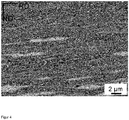
- the Figure 1 shows a picture with a scanning electron microscope (SEM) of a cross section through a six-fold cold-rolled Cu-Nb layer composite (N6) as an intermediate in the production of a film according to the invention.
- SEM scanning electron microscope
- N6 eight fold folded Cu-Nb layer composites (N8), twelve fold folded Cu-Nb layer composites (N12) and fourteen fold folded Cu-Nb layer composites (N14) are shown as cross sections.
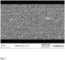
- FIGS 7 to 10 show photographs with a SEM of cross sections of films according to the invention made of Cu layers (dark) and Nb layers (light).
- the foils contain 19% by weight of Nb and the rest copper, including common impurities.
- a Cu-Nb layer composite is first produced by cold rolling from two 2 mm thick copper sheets and a 1 mm thick niobium sheet.
- the copper sheets and the niobium sheet were rolled as delivered.
- the copper sheets are made of OFE-Cu with the material designation "CW008A”.
- the niobium sheet consists of niobium with the material designation "R04200 type 1" and has an Nb content of at least 99.8% with up to 0.1% Ta and was supplied by WHS Sondermetalle eK.
- the layer composites are produced using an ARB process, as described in T. Nizolek et. al .: "Processing and Deformation Behavior of Bulk Cu-Nb Nanolaminates", Metallogr. Microstruct. Anal. (2014) 3, 470-476 is described.
- ARB cycle numbers of N4 (folded four times), N6 (folded six times), N8 (folded eight times) are used in the production of the layer composites; N12 (twelve folds) and N14 (fourteen folds) are used.
- N12 twelve folds
- N14 fourteen folds
- the laminates are ground as an intermediate product in a direction parallel to the thickness of the laminates.
- the films were also ground in a direction parallel to the thickness of the films.
- the contrast in the SEM is created by backscattered electrons, so that the niobium in the Figures 1 to 10 appears lighter than the copper.
- a Vickers hardness measurement was carried out in the direction of the thickness of the film and the electrical conductivity was measured in a direction perpendicular to the thickness of the film. The results of this are in Figure 11 shown.
- the Nb layers are in contrast to the Nb layers after Figure 1 no more than uniformly thick layers are present in the layer composite. Instead, a layer structure with localized Nb inclusions has been created in the folding and cold rolling process around which the Cu layers are arranged.
- the deformations of the Cu layers caused by the Nb inclusions and the Nb inclusions themselves also lead to a consolidation of the layer composite due to obstacles to the dislocation propagation in the material.
- the copper layers come into contact with each other at different points in the layer composite, so that the electrical conductivity is largely determined by the copper.
- a complete separation of the Nb layers is not desirable since the hardening effect is greater when the layer structure is still present.
- the Vickers hardness is slightly greater than for pure copper (Cu) from eight folds (N8), with only a slightly reduced electrical conductivity compared to pure copper. Twelve folds (N12) and fourteen folds (N14) result in a significantly higher Vickers hardness, which also exceeds the Vickers hardness of pure niobium (Nb). At the same time, there is an electrical conductivity that is above 15 MS / m and thus not very far below that of pure copper but above that of pure niobium. As can be seen from the measurements for N12 and N14, further folding does not necessarily lead to a significantly higher Vickers hardness with a simultaneous decrease in electrical conductivity. Therefore, according to the invention, ten to fourteen folds (N10 to N14) are preferred. Twelve folds (N12) are very particularly preferred.
- the Vickers hardness HV0.1 is used for the in Figure 11 shown measured values measured with a force of 0.1 N in the direction of the thickness of the film.
- the Vickers hardness is measured in accordance with DIN EN ISO 6507-1: 2018 to -4: 2018: DIN German Institute for Standardization eV: Metallic materials - Vickers hardness test - Part 1: Test method. It is a Vickers micro hardness test.
- the electrical conductivity is determined by a four-point measurement method.
- the films N8 and especially N12 and N14 according to the invention are notable for high hardness and good electrical conductivity.
- the foils with a thickness of approx. 43 ⁇ m are so thin that they can be made directly from the foils produced in this way Test needles or bond wires can be obtained by cutting them out of the foils.
- the thin Cu layers and Nb layers result in a largely homogeneous material across the cross section of the film.
- the test needles made of the foils wear out slowly due to their hardness and at the same time conduct the electrical current well for testing a contact, so that a large number of electrical contacts can be tested with high sensitivity of the measurement before the test needles have to be replaced.
- test pins or bond wires can be coated with an oxidation-resistant metal for surface treatment.
- gold, platinum or palladium can be used.
Landscapes
- Engineering & Computer Science (AREA)
- Computer Hardware Design (AREA)
- Microelectronics & Electronic Packaging (AREA)
- Power Engineering (AREA)
- Mechanical Engineering (AREA)
- Manufacturing & Machinery (AREA)
- Non-Insulated Conductors (AREA)
- Parts Printed On Printed Circuit Boards (AREA)
- Conductive Materials (AREA)
Priority Applications (3)
| Application Number | Priority Date | Filing Date | Title |
|---|---|---|---|
| EP19151346.4A EP3680101B1 (fr) | 2019-01-11 | 2019-01-11 | Feuille de métal réfractaire / cuivre durcie et son procédé de fabrication |
| TW109100394A TW202100765A (zh) | 2019-01-11 | 2020-01-07 | 經塗覆的銅/耐火金屬箔及其製造方法 |
| PCT/EP2020/050537 WO2020144322A1 (fr) | 2019-01-11 | 2020-01-10 | Feuille en cuivre / métal réfractaire revêtue et son procédé de fabrication |
Applications Claiming Priority (1)
| Application Number | Priority Date | Filing Date | Title |
|---|---|---|---|
| EP19151346.4A EP3680101B1 (fr) | 2019-01-11 | 2019-01-11 | Feuille de métal réfractaire / cuivre durcie et son procédé de fabrication |
Publications (2)
| Publication Number | Publication Date |
|---|---|
| EP3680101A1 true EP3680101A1 (fr) | 2020-07-15 |
| EP3680101B1 EP3680101B1 (fr) | 2022-03-02 |
Family
ID=65019356
Family Applications (1)
| Application Number | Title | Priority Date | Filing Date |
|---|---|---|---|
| EP19151346.4A Active EP3680101B1 (fr) | 2019-01-11 | 2019-01-11 | Feuille de métal réfractaire / cuivre durcie et son procédé de fabrication |
Country Status (3)
| Country | Link |
|---|---|
| EP (1) | EP3680101B1 (fr) |
| TW (1) | TW202100765A (fr) |
| WO (1) | WO2020144322A1 (fr) |
Citations (6)
| Publication number | Priority date | Publication date | Assignee | Title |
|---|---|---|---|---|
| EP2060921A1 (fr) | 2007-11-16 | 2009-05-20 | Technoprobe S.p.A | Sonde de contact pour tête de test à sondes verticales et tête de test correspondante pour tester la performance électrique de microstructures |
| US20100194415A1 (en) | 2007-09-27 | 2010-08-05 | Kabushiki Kaisha Toshiba | Probe needle material, probe needle and probe card each using the same, and inspection process |
| US20120286816A1 (en) | 2004-05-21 | 2012-11-15 | Microprobe, Inc. | Probes with high current carrying capability and laser machining methods |
| US20130099813A1 (en) | 2011-10-21 | 2013-04-25 | Tokyo Electron Limited | Contact terminal for a probe card, and the probe card |
| US20140266278A1 (en) | 2013-03-18 | 2014-09-18 | Cheng Yun Technology Co., Ltd. | Probe needle |
| WO2016009293A1 (fr) | 2014-07-14 | 2016-01-21 | Technoprobe S.P.A. | Sonde de contact pour une tête d'essai et procédé de fabrication correspondant |
-
2019
- 2019-01-11 EP EP19151346.4A patent/EP3680101B1/fr active Active
-
2020
- 2020-01-07 TW TW109100394A patent/TW202100765A/zh unknown
- 2020-01-10 WO PCT/EP2020/050537 patent/WO2020144322A1/fr active Application Filing
Patent Citations (6)
| Publication number | Priority date | Publication date | Assignee | Title |
|---|---|---|---|---|
| US20120286816A1 (en) | 2004-05-21 | 2012-11-15 | Microprobe, Inc. | Probes with high current carrying capability and laser machining methods |
| US20100194415A1 (en) | 2007-09-27 | 2010-08-05 | Kabushiki Kaisha Toshiba | Probe needle material, probe needle and probe card each using the same, and inspection process |
| EP2060921A1 (fr) | 2007-11-16 | 2009-05-20 | Technoprobe S.p.A | Sonde de contact pour tête de test à sondes verticales et tête de test correspondante pour tester la performance électrique de microstructures |
| US20130099813A1 (en) | 2011-10-21 | 2013-04-25 | Tokyo Electron Limited | Contact terminal for a probe card, and the probe card |
| US20140266278A1 (en) | 2013-03-18 | 2014-09-18 | Cheng Yun Technology Co., Ltd. | Probe needle |
| WO2016009293A1 (fr) | 2014-07-14 | 2016-01-21 | Technoprobe S.P.A. | Sonde de contact pour une tête d'essai et procédé de fabrication correspondant |
Non-Patent Citations (11)
| Title |
|---|
| BSI: "British Standard Specification for Copper for Electrical Purposes", 31 December 1985 (1985-12-31), XP055594198, Retrieved from the Internet <URL:https://allcivilstandard.com/wp-content/uploads/2019/02/BS-01434-1985-scan.pdf> [retrieved on 20190605] * |
| I.J. BEYERLEIN ET AL.: "Interface-driven microstructure development and ultra high strength of bulk nanostructured Cu-Nb multilayers", J. MATER. RES., vol. 28, no. 13, 14 July 2013 (2013-07-14) |
| J.M. WHEELER ET AL., CURR OPIN SOLID ST M, vol. 19, 2015, pages 354 - 366 |
| JOHN S. CARPENTER ET AL: "Processing Parameter Influence on Texture and Microstructural Evolution in Cu-Nb Multilayer Composites Fabricated via Accumulative Roll Bonding", METALLURGICAL AND MATERIALS TRANSACTIONS A: PHYSICAL METALLURGY & MATERIALS SCIENCE., vol. 45, no. 4, 10 January 2014 (2014-01-10), US, pages 2192 - 2208, XP055593776, ISSN: 1073-5623, DOI: 10.1007/s11661-013-2162-4 * |
| LIM S C V ET AL: "Length scale effects on recrystallization and texture evolution in Cu layers of a roll-bonded Cu-Nb composite", MATERIALS SCIENCE AND ENGINEERING: A, ELSEVIER, AMSTERDAM, NL, vol. 520, no. 1-2, 15 September 2009 (2009-09-15), pages 189 - 196, XP026350114, ISSN: 0921-5093, [retrieved on 20090522] * |
| MARA ET AL: "Tensile behavior of 40nm Cu/Nb nanoscale multilayers", SCRIPTA MATERIALIA, ELSEVIER, AMSTERDAM, NL, vol. 58, no. 10, 11 January 2008 (2008-01-11), pages 874 - 877, XP022527526, ISSN: 1359-6462, DOI: 10.1016/J.SCRIPTAMAT.2008.01.005 * |
| PANTSYRNY V I ET AL: "High Strength, High Conductivity Microcomposite Cu-Nb Wires with Cross Sections in the Range of 0.01-100", IEEE TRANSACTIONS ON APPLIED SUPERCONDUCTIVITY, IEEE SERVICE CENTER, LOS ALAMITOS, CA, US, vol. 17, no. 2, 1 June 2008 (2008-06-01), pages 616 - 619, XP011214737, ISSN: 1051-8223 * |
| S.C JHA ET AL: "High-strength high-conductivity Cu-Nb microcomposite sheet fabricated via multiple roll bonding", METALLURGICAL TRANSACTIONS A- PHYSICAL METALLURGY AND MATERIALS SCIENCE, vol. 24:1, 2 January 1993 (1993-01-02), US, pages 15 - 20, XP055594121, ISSN: 0360-2133, DOI: 10.1007/BF02669597 * |
| T. NIZOLEK: "Processing and Deformation Behavior of Bulk Cu-Nb Nanolaminates", METALLOGR. MICROSTRUCT. ANAL., vol. 3, 2014, pages 470 - 476 |
| T. NIZOLEK; N.A. MARA; I.J. BEYERLEIN; J.T. AVALLONE; J.E. SCOTT; T.M. POLLOCK: "Processing and Deformation Behavior of Bulk Cu-Nb Nanolaminates", METALLOGR. MICROSTRUCT. ANAL., vol. 3, 2014, pages 470 - 476 |
| W. C. OLIVER; G. M. PHARR, JOURNAL OF MATERIALS RESEARCH, vol. 1564, 1992 |
Also Published As
| Publication number | Publication date |
|---|---|
| EP3680101B1 (fr) | 2022-03-02 |
| WO2020144322A1 (fr) | 2020-07-16 |
| TW202100765A (zh) | 2021-01-01 |
Similar Documents
| Publication | Publication Date | Title |
|---|---|---|
| DE602005002898T2 (de) | Kupferlegierung und Verfahren zu deren Herstellung | |
| DE112010001811B4 (de) | Cu-Ni-Si-Mg-Legierung mit verbesserter Leitfähigkeit und Biegbarkeit | |
| DE69933255T2 (de) | Kupferlegierungsblech für elektronische Teile | |
| EP2193867B2 (fr) | Méthode de fabrication d'une électrode en fil d'acier destinée à la coupe par étincelage. | |
| DE69624274T2 (de) | Verbundene Gegenstände, korrosionsbeständiges Verbindungsmaterial und Herstellungsverfahren dieser Gegenstände | |
| EP2137330B1 (fr) | Feuille métallique | |
| DE112012006189T5 (de) | Plattiertes Element, plattierter Anschluss für einen Verbinder, Verfahren zum Herstellen eines plattierten Elementes und Verfahren zum Herstellen eines plattierten Anschlusses für einen Verbinder | |
| DE69703420T2 (de) | Produkt aus AlMgMn-Legierung für Schweissstrukturen mit verbesserter Korossionsbeständigkeit | |
| DE10147968B4 (de) | Kupferlegierung von hoher mechanischer Festigkeit | |
| EP1488827A1 (fr) | Procédé de fabrication de structures d'électrodes ainsi qu'une structure d'électrode et son utilisation | |
| DE102010012609A1 (de) | Sn-plattiertes Kupfer oder Sn-plattierte Kupferlegierung mit hervorragender Wärmebeständigkeit und Herstellungsverfahren dafür | |
| EP3425665B1 (fr) | Procédé de fabrication d'un fils de connexion | |
| DE3520407C2 (de) | Verfahren zur thermomechanischen Behandlung von kobalthaltigen Kupfer-Beryllium-Legierungen | |
| DE112012002864B4 (de) | Elektrodenmaterial für Temperatursicherungen und Herstellungsverfahren derselben sowie Temperatursicherung, die das Elektrodenmaterial verwendet | |
| EP3960890A1 (fr) | Alliage palladium-cuivre-argent-ruthénium | |
| DE102010007624B4 (de) | Separator für eine Brennstoffzelle und Verfahren zu dessen Herstellung | |
| DE112021002136T5 (de) | Legierung für einen Widerstand und Verwendung einer Widerstandslegierung in einem Widerstand | |
| DE112020002118T5 (de) | Aluminiumbasisdraht, Litzendraht, und Verfahren zur Herstellung von Aluminiumbasisdraht | |
| DE3522118C2 (fr) | ||
| EP3862759B1 (fr) | Fil enrobe et procédé de fabrication de fil enrobe | |
| WO2021180421A1 (fr) | Fil et bande comprenant des nanotubes de nitrure de bore pour contacts électriques | |
| EP2668311B1 (fr) | Bande d'aluminium à haute conductivité thermique et electrique | |
| DE102020004695A1 (de) | Elektrisches kontaktmaterial, anschlusspassstück, verbinder und kabelbaum | |
| EP3680101B1 (fr) | Feuille de métal réfractaire / cuivre durcie et son procédé de fabrication | |
| DE112005001271T5 (de) | Kupferlegierung für elektrische und elektronische Geräte |
Legal Events
| Date | Code | Title | Description |
|---|---|---|---|
| PUAI | Public reference made under article 153(3) epc to a published international application that has entered the european phase |
Free format text: ORIGINAL CODE: 0009012 |
|
| STAA | Information on the status of an ep patent application or granted ep patent |
Free format text: STATUS: REQUEST FOR EXAMINATION WAS MADE |
|
| 17P | Request for examination filed |
Effective date: 20190129 |
|
| AK | Designated contracting states |
Kind code of ref document: A1 Designated state(s): AL AT BE BG CH CY CZ DE DK EE ES FI FR GB GR HR HU IE IS IT LI LT LU LV MC MK MT NL NO PL PT RO RS SE SI SK SM TR |
|
| AX | Request for extension of the european patent |
Extension state: BA ME |
|
| STAA | Information on the status of an ep patent application or granted ep patent |
Free format text: STATUS: EXAMINATION IS IN PROGRESS |
|
| 17Q | First examination report despatched |
Effective date: 20210211 |
|
| RIC1 | Information provided on ipc code assigned before grant |
Ipc: B32B 15/01 20060101AFI20210412BHEP Ipc: B32B 15/20 20060101ALI20210412BHEP Ipc: B32B 38/00 20060101ALI20210412BHEP Ipc: H01L 23/00 20060101ALI20210412BHEP Ipc: C22C 9/00 20060101ALN20210412BHEP Ipc: B32B 7/05 20190101ALN20210412BHEP Ipc: G01R 3/00 20060101ALN20210412BHEP |
|
| GRAP | Despatch of communication of intention to grant a patent |
Free format text: ORIGINAL CODE: EPIDOSNIGR1 |
|
| STAA | Information on the status of an ep patent application or granted ep patent |
Free format text: STATUS: GRANT OF PATENT IS INTENDED |
|
| GRAJ | Information related to disapproval of communication of intention to grant by the applicant or resumption of examination proceedings by the epo deleted |
Free format text: ORIGINAL CODE: EPIDOSDIGR1 |
|
| STAA | Information on the status of an ep patent application or granted ep patent |
Free format text: STATUS: EXAMINATION IS IN PROGRESS |
|
| RIC1 | Information provided on ipc code assigned before grant |
Ipc: B32B 15/01 20060101AFI20210514BHEP Ipc: B32B 15/20 20060101ALI20210514BHEP Ipc: B32B 38/00 20060101ALI20210514BHEP Ipc: H01L 23/00 20060101ALI20210514BHEP Ipc: C22C 9/00 20060101ALN20210514BHEP Ipc: B32B 7/05 20190101ALN20210514BHEP Ipc: G01R 3/00 20060101ALN20210514BHEP |
|
| INTG | Intention to grant announced |
Effective date: 20210602 |
|
| INTC | Intention to grant announced (deleted) | ||
| GRAP | Despatch of communication of intention to grant a patent |
Free format text: ORIGINAL CODE: EPIDOSNIGR1 |
|
| STAA | Information on the status of an ep patent application or granted ep patent |
Free format text: STATUS: GRANT OF PATENT IS INTENDED |
|
| RIC1 | Information provided on ipc code assigned before grant |
Ipc: G01R 3/00 20060101ALN20210914BHEP Ipc: B32B 7/05 20190101ALN20210914BHEP Ipc: C22C 9/00 20060101ALN20210914BHEP Ipc: H01L 23/00 20060101ALI20210914BHEP Ipc: B32B 38/00 20060101ALI20210914BHEP Ipc: B32B 15/20 20060101ALI20210914BHEP Ipc: B32B 15/01 20060101AFI20210914BHEP |
|
| INTG | Intention to grant announced |
Effective date: 20210928 |
|
| GRAS | Grant fee paid |
Free format text: ORIGINAL CODE: EPIDOSNIGR3 |
|
| RAP3 | Party data changed (applicant data changed or rights of an application transferred) |
Owner name: HERAEUS DEUTSCHLAND GMBH & CO. KG |
|
| GRAA | (expected) grant |
Free format text: ORIGINAL CODE: 0009210 |
|
| STAA | Information on the status of an ep patent application or granted ep patent |
Free format text: STATUS: THE PATENT HAS BEEN GRANTED |
|
| AK | Designated contracting states |
Kind code of ref document: B1 Designated state(s): AL AT BE BG CH CY CZ DE DK EE ES FI FR GB GR HR HU IE IS IT LI LT LU LV MC MK MT NL NO PL PT RO RS SE SI SK SM TR |
|
| REG | Reference to a national code |
Ref country code: GB Ref legal event code: FG4D Free format text: NOT ENGLISH |
|
| REG | Reference to a national code |
Ref country code: CH Ref legal event code: EP Ref country code: AT Ref legal event code: REF Ref document number: 1471917 Country of ref document: AT Kind code of ref document: T Effective date: 20220315 |
|
| REG | Reference to a national code |
Ref country code: DE Ref legal event code: R096 Ref document number: 502019003516 Country of ref document: DE |
|
| REG | Reference to a national code |
Ref country code: IE Ref legal event code: FG4D Free format text: LANGUAGE OF EP DOCUMENT: GERMAN |
|
| REG | Reference to a national code |
Ref country code: LT Ref legal event code: MG9D |
|
| REG | Reference to a national code |
Ref country code: NL Ref legal event code: MP Effective date: 20220302 |
|
| PG25 | Lapsed in a contracting state [announced via postgrant information from national office to epo] |
Ref country code: SE Free format text: LAPSE BECAUSE OF FAILURE TO SUBMIT A TRANSLATION OF THE DESCRIPTION OR TO PAY THE FEE WITHIN THE PRESCRIBED TIME-LIMIT Effective date: 20220302 Ref country code: RS Free format text: LAPSE BECAUSE OF FAILURE TO SUBMIT A TRANSLATION OF THE DESCRIPTION OR TO PAY THE FEE WITHIN THE PRESCRIBED TIME-LIMIT Effective date: 20220302 Ref country code: NO Free format text: LAPSE BECAUSE OF FAILURE TO SUBMIT A TRANSLATION OF THE DESCRIPTION OR TO PAY THE FEE WITHIN THE PRESCRIBED TIME-LIMIT Effective date: 20220602 Ref country code: LT Free format text: LAPSE BECAUSE OF FAILURE TO SUBMIT A TRANSLATION OF THE DESCRIPTION OR TO PAY THE FEE WITHIN THE PRESCRIBED TIME-LIMIT Effective date: 20220302 Ref country code: HR Free format text: LAPSE BECAUSE OF FAILURE TO SUBMIT A TRANSLATION OF THE DESCRIPTION OR TO PAY THE FEE WITHIN THE PRESCRIBED TIME-LIMIT Effective date: 20220302 Ref country code: ES Free format text: LAPSE BECAUSE OF FAILURE TO SUBMIT A TRANSLATION OF THE DESCRIPTION OR TO PAY THE FEE WITHIN THE PRESCRIBED TIME-LIMIT Effective date: 20220302 Ref country code: BG Free format text: LAPSE BECAUSE OF FAILURE TO SUBMIT A TRANSLATION OF THE DESCRIPTION OR TO PAY THE FEE WITHIN THE PRESCRIBED TIME-LIMIT Effective date: 20220602 |
|
| PG25 | Lapsed in a contracting state [announced via postgrant information from national office to epo] |
Ref country code: PL Free format text: LAPSE BECAUSE OF FAILURE TO SUBMIT A TRANSLATION OF THE DESCRIPTION OR TO PAY THE FEE WITHIN THE PRESCRIBED TIME-LIMIT Effective date: 20220302 Ref country code: LV Free format text: LAPSE BECAUSE OF FAILURE TO SUBMIT A TRANSLATION OF THE DESCRIPTION OR TO PAY THE FEE WITHIN THE PRESCRIBED TIME-LIMIT Effective date: 20220302 Ref country code: GR Free format text: LAPSE BECAUSE OF FAILURE TO SUBMIT A TRANSLATION OF THE DESCRIPTION OR TO PAY THE FEE WITHIN THE PRESCRIBED TIME-LIMIT Effective date: 20220603 Ref country code: FI Free format text: LAPSE BECAUSE OF FAILURE TO SUBMIT A TRANSLATION OF THE DESCRIPTION OR TO PAY THE FEE WITHIN THE PRESCRIBED TIME-LIMIT Effective date: 20220302 |
|
| PG25 | Lapsed in a contracting state [announced via postgrant information from national office to epo] |
Ref country code: NL Free format text: LAPSE BECAUSE OF FAILURE TO SUBMIT A TRANSLATION OF THE DESCRIPTION OR TO PAY THE FEE WITHIN THE PRESCRIBED TIME-LIMIT Effective date: 20220302 |
|
| PG25 | Lapsed in a contracting state [announced via postgrant information from national office to epo] |
Ref country code: SM Free format text: LAPSE BECAUSE OF FAILURE TO SUBMIT A TRANSLATION OF THE DESCRIPTION OR TO PAY THE FEE WITHIN THE PRESCRIBED TIME-LIMIT Effective date: 20220302 Ref country code: SK Free format text: LAPSE BECAUSE OF FAILURE TO SUBMIT A TRANSLATION OF THE DESCRIPTION OR TO PAY THE FEE WITHIN THE PRESCRIBED TIME-LIMIT Effective date: 20220302 Ref country code: RO Free format text: LAPSE BECAUSE OF FAILURE TO SUBMIT A TRANSLATION OF THE DESCRIPTION OR TO PAY THE FEE WITHIN THE PRESCRIBED TIME-LIMIT Effective date: 20220302 Ref country code: PT Free format text: LAPSE BECAUSE OF FAILURE TO SUBMIT A TRANSLATION OF THE DESCRIPTION OR TO PAY THE FEE WITHIN THE PRESCRIBED TIME-LIMIT Effective date: 20220704 Ref country code: EE Free format text: LAPSE BECAUSE OF FAILURE TO SUBMIT A TRANSLATION OF THE DESCRIPTION OR TO PAY THE FEE WITHIN THE PRESCRIBED TIME-LIMIT Effective date: 20220302 Ref country code: CZ Free format text: LAPSE BECAUSE OF FAILURE TO SUBMIT A TRANSLATION OF THE DESCRIPTION OR TO PAY THE FEE WITHIN THE PRESCRIBED TIME-LIMIT Effective date: 20220302 |
|
| PG25 | Lapsed in a contracting state [announced via postgrant information from national office to epo] |
Ref country code: IS Free format text: LAPSE BECAUSE OF FAILURE TO SUBMIT A TRANSLATION OF THE DESCRIPTION OR TO PAY THE FEE WITHIN THE PRESCRIBED TIME-LIMIT Effective date: 20220702 Ref country code: AL Free format text: LAPSE BECAUSE OF FAILURE TO SUBMIT A TRANSLATION OF THE DESCRIPTION OR TO PAY THE FEE WITHIN THE PRESCRIBED TIME-LIMIT Effective date: 20220302 |
|
| REG | Reference to a national code |
Ref country code: DE Ref legal event code: R097 Ref document number: 502019003516 Country of ref document: DE |
|
| PLBE | No opposition filed within time limit |
Free format text: ORIGINAL CODE: 0009261 |
|
| STAA | Information on the status of an ep patent application or granted ep patent |
Free format text: STATUS: NO OPPOSITION FILED WITHIN TIME LIMIT |
|
| PG25 | Lapsed in a contracting state [announced via postgrant information from national office to epo] |
Ref country code: DK Free format text: LAPSE BECAUSE OF FAILURE TO SUBMIT A TRANSLATION OF THE DESCRIPTION OR TO PAY THE FEE WITHIN THE PRESCRIBED TIME-LIMIT Effective date: 20220302 |
|
| 26N | No opposition filed |
Effective date: 20221205 |
|
| PG25 | Lapsed in a contracting state [announced via postgrant information from national office to epo] |
Ref country code: SI Free format text: LAPSE BECAUSE OF FAILURE TO SUBMIT A TRANSLATION OF THE DESCRIPTION OR TO PAY THE FEE WITHIN THE PRESCRIBED TIME-LIMIT Effective date: 20220302 |
|
| PGFP | Annual fee paid to national office [announced via postgrant information from national office to epo] |
Ref country code: IT Payment date: 20230120 Year of fee payment: 5 Ref country code: GB Payment date: 20230119 Year of fee payment: 5 Ref country code: DE Payment date: 20230123 Year of fee payment: 5 |
|
| P01 | Opt-out of the competence of the unified patent court (upc) registered |
Effective date: 20230527 |
|
| REG | Reference to a national code |
Ref country code: CH Ref legal event code: PL |
|
| PG25 | Lapsed in a contracting state [announced via postgrant information from national office to epo] |
Ref country code: LU Free format text: LAPSE BECAUSE OF NON-PAYMENT OF DUE FEES Effective date: 20230111 |
|
| REG | Reference to a national code |
Ref country code: BE Ref legal event code: MM Effective date: 20230131 |
|
| PG25 | Lapsed in a contracting state [announced via postgrant information from national office to epo] |
Ref country code: LI Free format text: LAPSE BECAUSE OF NON-PAYMENT OF DUE FEES Effective date: 20230131 Ref country code: CH Free format text: LAPSE BECAUSE OF NON-PAYMENT OF DUE FEES Effective date: 20230131 |
|
| PG25 | Lapsed in a contracting state [announced via postgrant information from national office to epo] |
Ref country code: FR Free format text: LAPSE BECAUSE OF NON-PAYMENT OF DUE FEES Effective date: 20230131 Ref country code: BE Free format text: LAPSE BECAUSE OF NON-PAYMENT OF DUE FEES Effective date: 20230131 |
|
| PG25 | Lapsed in a contracting state [announced via postgrant information from national office to epo] |
Ref country code: IE Free format text: LAPSE BECAUSE OF NON-PAYMENT OF DUE FEES Effective date: 20230111 |
|
| PG25 | Lapsed in a contracting state [announced via postgrant information from national office to epo] |
Ref country code: MC Free format text: LAPSE BECAUSE OF FAILURE TO SUBMIT A TRANSLATION OF THE DESCRIPTION OR TO PAY THE FEE WITHIN THE PRESCRIBED TIME-LIMIT Effective date: 20220302 |
|
| PG25 | Lapsed in a contracting state [announced via postgrant information from national office to epo] |
Ref country code: MC Free format text: LAPSE BECAUSE OF FAILURE TO SUBMIT A TRANSLATION OF THE DESCRIPTION OR TO PAY THE FEE WITHIN THE PRESCRIBED TIME-LIMIT Effective date: 20220302 |
|
| REG | Reference to a national code |
Ref country code: DE Ref legal event code: R119 Ref document number: 502019003516 Country of ref document: DE |