EP3675169A1 - Method for manufacturing flexible display panel, and flexible display panel - Google Patents
Method for manufacturing flexible display panel, and flexible display panel Download PDFInfo
- Publication number
- EP3675169A1 EP3675169A1 EP17922187.4A EP17922187A EP3675169A1 EP 3675169 A1 EP3675169 A1 EP 3675169A1 EP 17922187 A EP17922187 A EP 17922187A EP 3675169 A1 EP3675169 A1 EP 3675169A1
- Authority
- EP
- European Patent Office
- Prior art keywords
- layer
- display panel
- photoresist
- flexible display
- flexible
- Prior art date
- Legal status (The legal status is an assumption and is not a legal conclusion. Google has not performed a legal analysis and makes no representation as to the accuracy of the status listed.)
- Withdrawn
Links
Images


Classifications
-
- H—ELECTRICITY
- H10—SEMICONDUCTOR DEVICES; ELECTRIC SOLID-STATE DEVICES NOT OTHERWISE PROVIDED FOR
- H10D—INORGANIC ELECTRIC SEMICONDUCTOR DEVICES
- H10D86/00—Integrated devices formed in or on insulating or conducting substrates, e.g. formed in silicon-on-insulator [SOI] substrates or on stainless steel or glass substrates
- H10D86/40—Integrated devices formed in or on insulating or conducting substrates, e.g. formed in silicon-on-insulator [SOI] substrates or on stainless steel or glass substrates characterised by multiple TFTs
- H10D86/411—Integrated devices formed in or on insulating or conducting substrates, e.g. formed in silicon-on-insulator [SOI] substrates or on stainless steel or glass substrates characterised by multiple TFTs characterised by materials, geometry or structure of the substrates
-
- H—ELECTRICITY
- H10—SEMICONDUCTOR DEVICES; ELECTRIC SOLID-STATE DEVICES NOT OTHERWISE PROVIDED FOR
- H10D—INORGANIC ELECTRIC SEMICONDUCTOR DEVICES
- H10D30/00—Field-effect transistors [FET]
- H10D30/60—Insulated-gate field-effect transistors [IGFET]
- H10D30/67—Thin-film transistors [TFT]
- H10D30/6704—Thin-film transistors [TFT] having supplementary regions or layers in the thin films or in the insulated bulk substrates for controlling properties of the device
- H10D30/6725—Thin-film transistors [TFT] having supplementary regions or layers in the thin films or in the insulated bulk substrates for controlling properties of the device having supplementary regions or layers for improving the flatness of the device
-
- H—ELECTRICITY
- H10—SEMICONDUCTOR DEVICES; ELECTRIC SOLID-STATE DEVICES NOT OTHERWISE PROVIDED FOR
- H10D—INORGANIC ELECTRIC SEMICONDUCTOR DEVICES
- H10D30/00—Field-effect transistors [FET]
- H10D30/60—Insulated-gate field-effect transistors [IGFET]
- H10D30/67—Thin-film transistors [TFT]
- H10D30/6758—Thin-film transistors [TFT] characterised by the insulating substrates
-
- H—ELECTRICITY
- H10—SEMICONDUCTOR DEVICES; ELECTRIC SOLID-STATE DEVICES NOT OTHERWISE PROVIDED FOR
- H10D—INORGANIC ELECTRIC SEMICONDUCTOR DEVICES
- H10D86/00—Integrated devices formed in or on insulating or conducting substrates, e.g. formed in silicon-on-insulator [SOI] substrates or on stainless steel or glass substrates
- H10D86/40—Integrated devices formed in or on insulating or conducting substrates, e.g. formed in silicon-on-insulator [SOI] substrates or on stainless steel or glass substrates characterised by multiple TFTs
- H10D86/441—Interconnections, e.g. scanning lines
- H10D86/443—Interconnections, e.g. scanning lines adapted for preventing breakage, peeling or short circuiting
-
- H—ELECTRICITY
- H10—SEMICONDUCTOR DEVICES; ELECTRIC SOLID-STATE DEVICES NOT OTHERWISE PROVIDED FOR
- H10D—INORGANIC ELECTRIC SEMICONDUCTOR DEVICES
- H10D86/00—Integrated devices formed in or on insulating or conducting substrates, e.g. formed in silicon-on-insulator [SOI] substrates or on stainless steel or glass substrates
- H10D86/40—Integrated devices formed in or on insulating or conducting substrates, e.g. formed in silicon-on-insulator [SOI] substrates or on stainless steel or glass substrates characterised by multiple TFTs
- H10D86/60—Integrated devices formed in or on insulating or conducting substrates, e.g. formed in silicon-on-insulator [SOI] substrates or on stainless steel or glass substrates characterised by multiple TFTs wherein the TFTs are in active matrices
-
- H—ELECTRICITY
- H10—SEMICONDUCTOR DEVICES; ELECTRIC SOLID-STATE DEVICES NOT OTHERWISE PROVIDED FOR
- H10K—ORGANIC ELECTRIC SOLID-STATE DEVICES
- H10K59/00—Integrated devices, or assemblies of multiple devices, comprising at least one organic light-emitting element covered by group H10K50/00
- H10K59/10—OLED displays
- H10K59/12—Active-matrix OLED [AMOLED] displays
- H10K59/121—Active-matrix OLED [AMOLED] displays characterised by the geometry or disposition of pixel elements
- H10K59/1213—Active-matrix OLED [AMOLED] displays characterised by the geometry or disposition of pixel elements the pixel elements being TFTs
-
- H—ELECTRICITY
- H10—SEMICONDUCTOR DEVICES; ELECTRIC SOLID-STATE DEVICES NOT OTHERWISE PROVIDED FOR
- H10K—ORGANIC ELECTRIC SOLID-STATE DEVICES
- H10K59/00—Integrated devices, or assemblies of multiple devices, comprising at least one organic light-emitting element covered by group H10K50/00
- H10K59/10—OLED displays
- H10K59/12—Active-matrix OLED [AMOLED] displays
- H10K59/122—Pixel-defining structures or layers, e.g. banks
-
- H—ELECTRICITY
- H10—SEMICONDUCTOR DEVICES; ELECTRIC SOLID-STATE DEVICES NOT OTHERWISE PROVIDED FOR
- H10K—ORGANIC ELECTRIC SOLID-STATE DEVICES
- H10K59/00—Integrated devices, or assemblies of multiple devices, comprising at least one organic light-emitting element covered by group H10K50/00
- H10K59/10—OLED displays
- H10K59/12—Active-matrix OLED [AMOLED] displays
- H10K59/123—Connection of the pixel electrodes to the thin film transistors [TFT]
-
- H—ELECTRICITY
- H10—SEMICONDUCTOR DEVICES; ELECTRIC SOLID-STATE DEVICES NOT OTHERWISE PROVIDED FOR
- H10K—ORGANIC ELECTRIC SOLID-STATE DEVICES
- H10K59/00—Integrated devices, or assemblies of multiple devices, comprising at least one organic light-emitting element covered by group H10K50/00
- H10K59/10—OLED displays
- H10K59/12—Active-matrix OLED [AMOLED] displays
- H10K59/124—Insulating layers formed between TFT elements and OLED elements
-
- H—ELECTRICITY
- H10—SEMICONDUCTOR DEVICES; ELECTRIC SOLID-STATE DEVICES NOT OTHERWISE PROVIDED FOR
- H10K—ORGANIC ELECTRIC SOLID-STATE DEVICES
- H10K59/00—Integrated devices, or assemblies of multiple devices, comprising at least one organic light-emitting element covered by group H10K50/00
- H10K59/10—OLED displays
- H10K59/12—Active-matrix OLED [AMOLED] displays
- H10K59/131—Interconnections, e.g. wiring lines or terminals
-
- H—ELECTRICITY
- H10—SEMICONDUCTOR DEVICES; ELECTRIC SOLID-STATE DEVICES NOT OTHERWISE PROVIDED FOR
- H10K—ORGANIC ELECTRIC SOLID-STATE DEVICES
- H10K71/00—Manufacture or treatment specially adapted for the organic devices covered by this subclass
- H10K71/20—Changing the shape of the active layer in the devices, e.g. patterning
- H10K71/221—Changing the shape of the active layer in the devices, e.g. patterning by lift-off techniques
-
- H—ELECTRICITY
- H10—SEMICONDUCTOR DEVICES; ELECTRIC SOLID-STATE DEVICES NOT OTHERWISE PROVIDED FOR
- H10K—ORGANIC ELECTRIC SOLID-STATE DEVICES
- H10K71/00—Manufacture or treatment specially adapted for the organic devices covered by this subclass
- H10K71/60—Forming conductive regions or layers, e.g. electrodes
-
- H—ELECTRICITY
- H10—SEMICONDUCTOR DEVICES; ELECTRIC SOLID-STATE DEVICES NOT OTHERWISE PROVIDED FOR
- H10K—ORGANIC ELECTRIC SOLID-STATE DEVICES
- H10K71/00—Manufacture or treatment specially adapted for the organic devices covered by this subclass
- H10K71/621—Providing a shape to conductive layers, e.g. patterning or selective deposition
-
- H—ELECTRICITY
- H10—SEMICONDUCTOR DEVICES; ELECTRIC SOLID-STATE DEVICES NOT OTHERWISE PROVIDED FOR
- H10K—ORGANIC ELECTRIC SOLID-STATE DEVICES
- H10K77/00—Constructional details of devices covered by this subclass and not covered by groups H10K10/80, H10K30/80, H10K50/80 or H10K59/80
- H10K77/10—Substrates, e.g. flexible substrates
- H10K77/111—Flexible substrates
-
- H—ELECTRICITY
- H10—SEMICONDUCTOR DEVICES; ELECTRIC SOLID-STATE DEVICES NOT OTHERWISE PROVIDED FOR
- H10K—ORGANIC ELECTRIC SOLID-STATE DEVICES
- H10K2102/00—Constructional details relating to the organic devices covered by this subclass
- H10K2102/301—Details of OLEDs
- H10K2102/311—Flexible OLED
-
- H—ELECTRICITY
- H10—SEMICONDUCTOR DEVICES; ELECTRIC SOLID-STATE DEVICES NOT OTHERWISE PROVIDED FOR
- H10K—ORGANIC ELECTRIC SOLID-STATE DEVICES
- H10K2102/00—Constructional details relating to the organic devices covered by this subclass
- H10K2102/301—Details of OLEDs
- H10K2102/351—Thickness
-
- H—ELECTRICITY
- H10—SEMICONDUCTOR DEVICES; ELECTRIC SOLID-STATE DEVICES NOT OTHERWISE PROVIDED FOR
- H10K—ORGANIC ELECTRIC SOLID-STATE DEVICES
- H10K59/00—Integrated devices, or assemblies of multiple devices, comprising at least one organic light-emitting element covered by group H10K50/00
- H10K59/10—OLED displays
- H10K59/12—Active-matrix OLED [AMOLED] displays
- H10K59/1201—Manufacture or treatment
-
- H—ELECTRICITY
- H10—SEMICONDUCTOR DEVICES; ELECTRIC SOLID-STATE DEVICES NOT OTHERWISE PROVIDED FOR
- H10K—ORGANIC ELECTRIC SOLID-STATE DEVICES
- H10K71/00—Manufacture or treatment specially adapted for the organic devices covered by this subclass
-
- Y—GENERAL TAGGING OF NEW TECHNOLOGICAL DEVELOPMENTS; GENERAL TAGGING OF CROSS-SECTIONAL TECHNOLOGIES SPANNING OVER SEVERAL SECTIONS OF THE IPC; TECHNICAL SUBJECTS COVERED BY FORMER USPC CROSS-REFERENCE ART COLLECTIONS [XRACs] AND DIGESTS
- Y02—TECHNOLOGIES OR APPLICATIONS FOR MITIGATION OR ADAPTATION AGAINST CLIMATE CHANGE
- Y02E—REDUCTION OF GREENHOUSE GAS [GHG] EMISSIONS, RELATED TO ENERGY GENERATION, TRANSMISSION OR DISTRIBUTION
- Y02E10/00—Energy generation through renewable energy sources
- Y02E10/50—Photovoltaic [PV] energy
- Y02E10/549—Organic PV cells
-
- Y—GENERAL TAGGING OF NEW TECHNOLOGICAL DEVELOPMENTS; GENERAL TAGGING OF CROSS-SECTIONAL TECHNOLOGIES SPANNING OVER SEVERAL SECTIONS OF THE IPC; TECHNICAL SUBJECTS COVERED BY FORMER USPC CROSS-REFERENCE ART COLLECTIONS [XRACs] AND DIGESTS
- Y02—TECHNOLOGIES OR APPLICATIONS FOR MITIGATION OR ADAPTATION AGAINST CLIMATE CHANGE
- Y02P—CLIMATE CHANGE MITIGATION TECHNOLOGIES IN THE PRODUCTION OR PROCESSING OF GOODS
- Y02P70/00—Climate change mitigation technologies in the production process for final industrial or consumer products
- Y02P70/50—Manufacturing or production processes characterised by the final manufactured product
Definitions
- the present invention relates to the field of display technology, and more particular to a flexible display panel fabrication method and a flexible display panel.
- LCDs liquid crystal displays
- OLED organic light-emitting diode
- a liquid crystal display panel is generally made up of a color filter (CF) substrate, a thin-film transistor (TFT) array substrate, and a liquid crystal layer filled between the two substrates.
- the CF substrate and the TFT substrate are generally formed of a backing plate that is made of rigid glass so that the liquid crystal display panel that is made in the form of a flat panel may not be flexed.
- An OLED display panel is a kind of flexible display panel.
- the flexible display panel is made of a flexible material and may proceed with displaying in a state of being arbitrarily flexible and deformable.
- Flexible display panels, such as OLED have various advantages, such as lightweight, small size, being easy to carry, being resistant to high and low temperatures, being resistant to impact, excellent capability of shock resistance, being adapted to a wide range of operation conditions, being curvable, and having better art aesthetics for outside appearance, and are becoming a hot spot of research and study for academic institutes and research facility.
- a known flexible display panel generally comprises a flexible base plate on one side of which a TFT array, light emissive devices, and driver circuits that drive the TFT array are provided.
- the driver circuits that drive the TFT array also include scan lines.
- the driver circuits that include the scan lines may undergo curving and flexing with the surface of the flexible base plate and stress defects are induced and would affect normal performance of the TFTs and the light emissive devices.
- An objective of the present invention are to provide a flexible display panel fabrication method, which effectively reduces stress defects induced in scan lines during curving of a flexible display panel so as to improve the stability of the flexible display panel.
- Another objective of the present invention is to provide a flexible display panel, in which scan lines has reduced stress defects during curving of the flexible display panel so as to improve the stability of the flexible display panel.
- the present invention first provides a flexible display panel fabrication method, which comprises the following steps:
- the through holes each have opposite sidewalls each of which defines an angle that is an obtuse angle with respect to an undersurface of the photoresist zones and also defines an angle that is an acute angle with respect to an upper surface of the photoresist zones.
- the through holes each have a cross section that is an isosceles trapezoid, and isosceles trapezoid has a lower base that is greater than an upper base.
- the backing cavities have a depth of 300-3000nm.
- the backing cavities have a cross section that is rectangular.
- the metal patterns have a thickness that corresponds to the depth of the backing cavities.
- Step S6 comprises:
- the present invention also provides a flexible display panel, which comprises:
- the backing cavities have a depth of 300-3000nm and a cross section that is rectangular.
- the metal patterns has a thickness that corresponds to the depth of the backing cavities.
- the present invention further provides a flexible display panel fabrication method, which comprises the following steps:
- the efficacy of the present invention is that the present invention provides a flexible display panel fabrication method, which first subjects a photoresist layer to patterning to form a plurality of mutually spaced photoresist zones, wherein a through hole is formed between every two adjacent ones of the photoresist zones; and then, subjecting the flexible backing plate to cavity formation with the photoresist zones as a mask so as to form a plurality of mutually parallel backing cavities respectively at locations corresponding to the through holes; and then, depositing a metal film and subsequently removing the photoresist zones and portions of the metal layer located thereon to form a plurality of metal patterns that are embedded in the plurality of mutually parallel backing cavities, wherein each of the metal patterns comprises a scan line and a plurality of gate electrodes; and then, forming a plurality of TFTs that are arranged in an array and OLED light emissive elements.
- the method allows the scan lines and the gate electrodes to be embedded in the flexible backing plate so as to effectively reduce stress defects induced in the scan lines during curving of the flexible display panel and improve the stability of the flexible display panel.
- the present invention provides a flexible display panel, which comprises metal patterns that include scan lines and gate electrodes and are embedded in the baking cavities of a flexible backing plate so as to reduce stress defects induced in the scan lines during curving of the flexible display panel to thereby help improve stability of the flexible display panel.
- the present invention provides a flexible display panel fabrication method, which comprises the following steps:
- Step S6 comprises:
- the method described above allows the metal patterns 32 that include the scan lines 321 and the gate electrodes 322 to be embedded in the backing cavities 11 formed in the flexible backing plate 1 and this is equivalent to forming a combined film of the metal patterns 32 and the flexible backing plate 2.
- the scan lines 321 and the gate electrodes 322 are integrally combined with the flexible backing plate 1 as a unitary structure and this helps spread a stress induced in the scan lines 321 during curving of the display panel thereby effectively reducing stress defects induced in the scan lines 321 during curving of the flexible display panel and thus improving stability of the flexible display panel.
- the present invention also provides a flexible display panel that is fabricated with the above method.
- a flexible display panel which comprises:
- the gate electrode 322, the semiconductor active layer 52, the source electrode 531, and the drain electrode 532 form the TFT T ; and the anode 57, the organic emissive layer 58, and the cathode 59 form the OLED light emissive element D.
- the backing cavities 11 has a depth of 300-3000nm and a cross section that is rectangular, and the metal patterns 32 has a thickness that corresponds to the depth of the backing cavities 11.
- the flexible display panel of the present invention is structured such that the metal patterns 32 that include the scan lines 321 and the gate electrodes 322 is embedded in the backing cavities 11 formed in the flexible backing plate 1 and this is equivalent to forming a combined film of the metal patterns 32 and the flexible backing plate 2.
- the scan lines 321 and the gate electrodes 322 are integrally combined with the flexible backing plate 1 as a unitary structure and this helps spread a stress induced in the scan lines 321 during curving of the display panel thereby effectively reducing stress defects induced in the scan lines 321 during curving of the flexible display panel and thus improving stability of the flexible display panel.
- the present invention provides a flexible display panel fabrication method, which first subjects a photoresist layer to patterning to form a plurality of mutually spaced photoresist zones, wherein a through hole is formed between every two adjacent ones of the photoresist zones; and then, subjecting the flexible backing plate to cavity formation with the photoresist zones as a mask so as to form a plurality of mutually parallel backing cavities respectively at locations corresponding to the through holes; and then, depositing a metal film and subsequently removing the photoresist zones and portions of the metal layer located thereon to form a plurality of metal patterns that are embedded in the plurality of mutually parallel backing cavities, wherein each of the metal patterns comprises a scan line and a plurality of gate electrodes; and then, forming a plurality of TFTs that are arranged in an array and OLED light emissive elements.
- the method allows the scan lines and the gate electrodes to be embedded in the flexible backing plate so as to effectively reduce stress defects induced in the scan lines during curving of the flexible display panel and improve the stability of the flexible display panel.
- the present invention provides a flexible display panel, which comprises metal patterns that include scan lines and gate electrodes and are embedded in the baking cavities of a flexible backing plate so as to reduce stress defects induced in the scan lines during curving of the flexible display panel to thereby help improve stability of the flexible display panel.
Landscapes
- Engineering & Computer Science (AREA)
- Microelectronics & Electronic Packaging (AREA)
- Manufacturing & Machinery (AREA)
- Physics & Mathematics (AREA)
- Geometry (AREA)
- Electroluminescent Light Sources (AREA)
- Devices For Indicating Variable Information By Combining Individual Elements (AREA)
Abstract
Description
- The present invention relates to the field of display technology, and more particular to a flexible display panel fabrication method and a flexible display panel.
- In the field of display technology, flat panel displays, such as liquid crystal displays (LCDs) and organic light-emitting diode (OLED) displays, have gradually taken the place of cathode ray tube (CRT) displays.
- Further, a liquid crystal display panel is generally made up of a color filter (CF) substrate, a thin-film transistor (TFT) array substrate, and a liquid crystal layer filled between the two substrates. The CF substrate and the TFT substrate are generally formed of a backing plate that is made of rigid glass so that the liquid crystal display panel that is made in the form of a flat panel may not be flexed.
- An OLED display panel is a kind of flexible display panel. The flexible display panel is made of a flexible material and may proceed with displaying in a state of being arbitrarily flexible and deformable. Flexible display panels, such as OLED, have various advantages, such as lightweight, small size, being easy to carry, being resistant to high and low temperatures, being resistant to impact, excellent capability of shock resistance, being adapted to a wide range of operation conditions, being curvable, and having better art aesthetics for outside appearance, and are becoming a hot spot of research and study for academic institutes and research facility.
- A known flexible display panel generally comprises a flexible base plate on one side of which a TFT array, light emissive devices, and driver circuits that drive the TFT array are provided. The driver circuits that drive the TFT array also include scan lines. When the known flexible display panel is curved or flexed, the driver circuits that include the scan lines may undergo curving and flexing with the surface of the flexible base plate and stress defects are induced and would affect normal performance of the TFTs and the light emissive devices.
- Thus, the prior art still needs for further improvement and progress.
- An objective of the present invention are to provide a flexible display panel fabrication method, which effectively reduces stress defects induced in scan lines during curving of a flexible display panel so as to improve the stability of the flexible display panel.
- Another objective of the present invention is to provide a flexible display panel, in which scan lines has reduced stress defects during curving of the flexible display panel so as to improve the stability of the flexible display panel.
- To achieve the above objective, the present invention first provides a flexible display panel fabrication method, which comprises the following steps:
- Step S1: providing a flexible backing plate and depositing a photoresist layer on the flexible backing plate;
- Step S2: subjecting the photoresist layer to patterning so as to form a plurality of mutually spaced photoresist zones, wherein a through hole is formed in two adjacent ones of the photoresist zones;
- Step S3: subjecting the flexible backing plate to cavity formation conducted with the photoresist zones as a mask so as to form a plurality of mutually parallel backing cavities respectively at locations corresponding to the through holes;
- Step S4: depositing a metal film on the photoresist zones and the flexible backing plate to form a metal layer covering the photoresist zones and a plurality of metal patterns that are embedded in the plurality of mutually parallel backing cavities,
wherein each of the metal patterns comprises a scan line and a plurality of gate electrodes connected to the scan line; - Step S5: peeling off the photoresist zones to remove the photoresist zones and the metal layer located on the photoresist zones; and
- Step S6: forming a plurality of thin-film transistors (TFTs) that are arranged in an array on the flexible backing plate and each of the metal patterns embedded in the backing cavities and depositing organic light-emitting diode (OLED) light emissive elements on the plurality of TFTs that are arranged in an array.
- The through holes each have opposite sidewalls each of which defines an angle that is an obtuse angle with respect to an undersurface of the photoresist zones and also defines an angle that is an acute angle with respect to an upper surface of the photoresist zones.
- The through holes each have a cross section that is an isosceles trapezoid, and isosceles trapezoid has a lower base that is greater than an upper base.
- The backing cavities have a depth of 300-3000nm.
- The backing cavities have a cross section that is rectangular.
- The metal patterns have a thickness that corresponds to the depth of the backing cavities.
- Step S6 comprises:
- depositing a gate insulation layer on the flexible backing plate and the metal patterns;
- depositing a semiconductor active layer on the gate insulation layer;
- depositing and subjecting a metal film to patterning treatment so as to form a source electrode and a drain electrode that are respectively in contact engagement with two ends of the semiconductor active layer, wherein the gate electrode, the semiconductor active layer, the source electrode, and the drain electrode collectively form the TFT;
- sequentially depositing an interlayer insulation layer, a planarization layer, and an anode, wherein the anode is connected, through a via extending through the interlayer insulation layer and the planarization layer, to the drain electrode of the TFT;
- forming a patterned pixel isolation layer on the planarization layer and the anode, such that the pixel isolation layer covers portions of the planarization layer and the anode; and
- sequentially depositing an organic emissive layer and a cathode in an area defined by the pixel isolation layer, wherein the anode, the organic emissive layer, and the cathode collectively form the OLED light emissive element.
- The present invention also provides a flexible display panel, which comprises:
- a flexible backing plate, wherein the flexible backing plate comprises a plurality of mutually parallel backing cavities;
- a plurality of metal patterns respectively embedded in the plurality of mutually parallel backing cavities, wherein each of the metal patterns comprises a scan and a plurality of gate electrodes connected to the scan line;
- a plurality of thin-film transistors (TFTs) arranged in an array on the flexible backing plate and each of the metal patterns; and
- organic light-emitting diode (OLED) light emissive elements arranged on the plurality of TFTs that are arranged in an array.
- The backing cavities have a depth of 300-3000nm and a cross section that is rectangular.
- The metal patterns has a thickness that corresponds to the depth of the backing cavities.
- The present invention further provides a flexible display panel fabrication method, which comprises the following steps:
- Step S1: providing a flexible backing plate and depositing a photoresist layer on the flexible backing plate;
- Step S2: subjecting the photoresist layer to patterning so as to form a plurality of mutually spaced photoresist zones, wherein a through hole is formed in two adjacent ones of the photoresist zones;
- Step S3: subjecting the flexible backing plate to cavity formation conducted with the photoresist zones as a mask so as to form a plurality of mutually parallel backing cavities respectively at locations corresponding to the through holes;
- Step S4: depositing a metal film on the photoresist zones and the flexible backing plate to form a metal layer covering the photoresist zones and a plurality of metal patterns that are embedded in the plurality of mutually parallel backing cavities,
wherein each of the metal patterns comprises a scan line and a plurality of gate electrodes connected to the scan line; - Step S5: peeling off the photoresist zones to remove the photoresist zones and the metal layer located on the photoresist zones; and
- Step S6: forming a plurality of thin-film transistors (TFTs) that are arranged in an array on the flexible backing plate and each of the metal patterns embedded in the backing cavities and depositing organic light-emitting diode (OLED) light emissive elements on the plurality of TFTs that are arranged in an array;
wherein the through holes each have opposite sidewalls each of which defines an angle that is an obtuse angle with respect to an undersurface of the photoresist zones and also defines an angle that is an acute angle with respect to an upper surface of the photoresist zones;
wherein the through holes each have a cross section that is an isosceles trapezoid, and isosceles trapezoid has a lower base that is greater than an upper base;
wherein the backing cavities have a depth of 300-3000nm; and
wherein the metal patterns has a thickness that corresponds to the depth of the backing cavities. - The efficacy of the present invention is that the present invention provides a flexible display panel fabrication method, which first subjects a photoresist layer to patterning to form a plurality of mutually spaced photoresist zones, wherein a through hole is formed between every two adjacent ones of the photoresist zones; and then, subjecting the flexible backing plate to cavity formation with the photoresist zones as a mask so as to form a plurality of mutually parallel backing cavities respectively at locations corresponding to the through holes; and then, depositing a metal film and subsequently removing the photoresist zones and portions of the metal layer located thereon to form a plurality of metal patterns that are embedded in the plurality of mutually parallel backing cavities, wherein each of the metal patterns comprises a scan line and a plurality of gate electrodes; and then, forming a plurality of TFTs that are arranged in an array and OLED light emissive elements. The method allows the scan lines and the gate electrodes to be embedded in the flexible backing plate so as to effectively reduce stress defects induced in the scan lines during curving of the flexible display panel and improve the stability of the flexible display panel. The present invention provides a flexible display panel, which comprises metal patterns that include scan lines and gate electrodes and are embedded in the baking cavities of a flexible backing plate so as to reduce stress defects induced in the scan lines during curving of the flexible display panel to thereby help improve stability of the flexible display panel.
- For better understanding of the features and technical contents of the present invention, reference will be made to the following detailed description of the present invention and the attached drawings. However, the drawings are provided only for reference and illustration and are not intended to limit the present invention.
- In the drawings:
-
FIG 1 is a flow chart illustrating a flexible display panel fabrication method according to the present invention; -
FIG. 2 is a schematic view illustrating Step S1 of the flexible display panel fabrication method according to the present invention; -
FIG. 3 is a schematic view illustrating Step S2 of the flexible display panel fabrication method according to the present invention; -
FIG. 4 is a schematic view illustrating Step S3 of the flexible display panel fabrication method according to the present invention; -
FIG. 5 is a schematic view illustrating Step S4 of the flexible display panel fabrication method according to the present invention; -
FIG. 6 is a top plan view illustrating a metal pattern made in Step S4 of the flexible display panel fabrication method according to the present invention; -
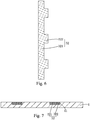
FIG. 7 is a schematic view illustrating Step S5 of the flexible display panel fabrication method according to the present invention; and -
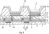
FIG. 8 is a schematic view illustrating Step S6 of the flexible display panel fabrication method according to the present invention and is also a schematic view illustrating a cross-sectional structure of a flexible display panel according to the present invention. - To further expound the technical solution adopted in the present invention and the advantages thereof, a detailed description will be given with reference to the preferred embodiments of the present invention and the drawings thereof.
- Referring to
FIG. 1 , firstly, the present invention provides a flexible display panel fabrication method, which comprises the following steps: - Step S1: as shown in
FIG. 2 , providing aflexible backing plate 1 and depositing aphotoresist layer 2 on theflexible backing plate 1.
Specifically, theflexible backing plate 1 is formed of a material comprising polyimide (PI) or polyethylene terephthalate (PET). - Step S2: as shown in
FIG. 3 , subjecting thephotoresist layer 2 to patterning through exposure and development so as to form a plurality of mutually spacedphotoresist zones 20, wherein a throughhole 21 is formed in two adjacent ones of thephotoresist zones 20.
It is noted here that the throughhole 21 has opposite sidewalls each defining an angle a, which is preferably an obtuse angle that is greater than 90°, with respect to an undersurface of thephotoresist zones 20 and also defining an angle b, which is preferably an acute angle that is sharp, with respect to an upper surface of thephotoresist zones 20.
Specifically, the throughhole 21 has a cross-section shape that is an isosceles trapezoid, wherein isosceles trapezoid has a lower base that is greater than an upper base and sides of isosceles trapezoid are inclined into interiority of the material of thephotoresist zones 20 while extending from top ends thereof toward the lower ends. - Step S3: as shown in
FIG. 4 , subjecting theflexible backing plate 1 to cavity formation through an etching operation conducted with thephotoresist zones 20 as a mask so as to form a plurality of mutuallyparallel backing cavities 11 respectively at locations corresponding to the through holes 21.
Specifically, thebacking cavities 11 have a depth, which is preferably, 300-3000nm in order to ensure the depth of thebacking cavities 11 is smaller than a thickness of theflexible backing plate 1. Further, thebacking cavities 11 have a cross-sectional shape that is rectangular. - Step S4: as shown in
FIG. 5 , depositing a metal film directly on thephotoresist zones 20 and theflexible backing plate 1, wherein since the sidewalls of the throughhole 21 define an angle a, which is an obtuse angle greater than 90°, with respect to the undersurface of thephotoresist zones 20 and an angle b, which is a sharp acute angle, with respect to the upper surface of and thephotoresist zones 2, the throughhole 21 effectively breaks and divides the metal film into ametal layer 31 that covers thephotoresist zones 20 and a plurality ofmetal patterns 32 that are embedded in the plurality of mutuallyparallel backing cavities 11 and show a pattern arrangement identical to thebacking cavities 11.
Further, themetal patterns 32 have a thickness that corresponds to the depth of thebacking cavities 11.
As shown inFIG. 6 , each of themetal patterns 32 comprises ascan line 321 and a plurality ofgate electrodes 322 connected to thescan line 321. - Step S5: as shown in
FIG. 7 , peeling off thephotoresist zones 20 so as to simultaneously remove themetal layer 31 that covers thephotoresist zones 20, while keeping the plurality ofmetal patterns 32 that are embedded in the plurality of mutuallyparallel backing cavities 11 and show a pattern arrangement identical to thebacking cavities 11.
In this process, since the throughholes 21 effectively break and divide the metal film, removal of thephotoresist zones 20 and the portion of the metal layer on thephotoresist zones 20 does not cause any damage to themetal patterns 32 embedded in thebacking cavities 11. - Step S6: as shown in
FIG. 8 , forming a plurality of thin-film transistors (TFTs) T that are arranged in an array on theflexible backing plate 1 and each of themetal patterns 32 embedded in thebacking cavities 11 and depositing organic light-emitting diode (OLED) light emissive elements D on the plurality of TFTs T that are arranged in an array, and finally conducting an encapsulation operation. - Specifically, Step S6 comprises:
- depositing a
gate insulation layer 51 on theflexible backing plate 1 and themetal patterns 32; - depositing a semiconductor
active layer 52 on thegate insulation layer 51; - depositing and subjecting a metal film to patterning treatment so as to form a
source electrode 531 and adrain electrode 532 that are respectively in contact engagement with two ends of the semiconductoractive layer 52, wherein thegate electrode 322, the semiconductoractive layer 52, thesource electrode 531, and thedrain electrode 532 collectively form the TFT T; - sequentially depositing an
interlayer insulation layer 54, aplanarization layer 55, and ananode 57, wherein theanode 57 is connected, through a via V extending through theinterlayer insulation layer 54 and theplanarization layer 55, to thedrain electrode 532 of the TFT T; - forming a patterned
pixel isolation layer 56 on theplanarization layer 55 and theanode 57, such that thepixel isolation layer 56 covers portions of theplanarization layer 55 and theanode 57; - sequentially depositing an organic
emissive layer 58 and acathode 59 in an area defined by thepixel isolation layer 56, wherein theanode 57, the organicemissive layer 58, and thecathode 59 collectively form the OLED light emissive element D. - The method described above allows the
metal patterns 32 that include thescan lines 321 and thegate electrodes 322 to be embedded in thebacking cavities 11 formed in theflexible backing plate 1 and this is equivalent to forming a combined film of themetal patterns 32 and theflexible backing plate 2. In other words, thescan lines 321 and thegate electrodes 322 are integrally combined with theflexible backing plate 1 as a unitary structure and this helps spread a stress induced in thescan lines 321 during curving of the display panel thereby effectively reducing stress defects induced in thescan lines 321 during curving of the flexible display panel and thus improving stability of the flexible display panel. - Based on the same inventive idea, the present invention also provides a flexible display panel that is fabricated with the above method. Referring to
FIG. 8 , in combination withFIG. 6 , the present invention provides a flexible display panel, which comprises: - a
flexible backing plate 1, wherein theflexible backing plate 1 comprises a plurality of mutuallyparallel backing cavities 11; - a plurality of
metal patterns 32 respectively embedded in the plurality of mutuallyparallel backing cavities 11, wherein each of themetal patterns 32 comprises ascan line 321 and a plurality ofgate electrodes 322 connected to thescan line 321; - a
gate insulation layer 51 set on and covering theflexible backing plate 1 and each of themetal patterns 32; - semiconductor
active layers 52 arranged on thegate insulation layer 51; - a
source electrode 531 and adrain electrode 532 respectively connected to two ends of each of the semiconductoractive layers 52; - an
interlayer insulation layer 54 set on and covering the semiconductoractive layers 52, thesource electrodes 531, thedrain electrodes 532, and thegate insulation layer 51; - a
planarization layer 55 set on and covering theinterlayer insulation layer 54; - an
anode 57 arranged on theplanarization layer 55 such that theanode 57 is connected to each of thedrain electrodes 532 through a via V extending through theinterlayer insulation layer 54 and theplanarization layer 55; - a
pixel isolation layer 56 set on and covering portions of theplanarization layer 55 and theanode 57; and - an organic
emissive layer 58 and thecathode 59 sequentially arranged, in a sequence from bottom to top, in an area defined by thepixel isolation layer 56. - The
gate electrode 322, the semiconductoractive layer 52, thesource electrode 531, and thedrain electrode 532 form the TFT T; and theanode 57, the organicemissive layer 58, and thecathode 59 form the OLED light emissive element D. - Specifically, the
backing cavities 11 has a depth of 300-3000nm and a cross section that is rectangular, and themetal patterns 32 has a thickness that corresponds to the depth of thebacking cavities 11. - Since the flexible display panel of the present invention is structured such that the
metal patterns 32 that include thescan lines 321 and thegate electrodes 322 is embedded in thebacking cavities 11 formed in theflexible backing plate 1 and this is equivalent to forming a combined film of themetal patterns 32 and theflexible backing plate 2. In other words, thescan lines 321 and thegate electrodes 322 are integrally combined with theflexible backing plate 1 as a unitary structure and this helps spread a stress induced in thescan lines 321 during curving of the display panel thereby effectively reducing stress defects induced in thescan lines 321 during curving of the flexible display panel and thus improving stability of the flexible display panel. - In summary, the present invention provides a flexible display panel fabrication method, which first subjects a photoresist layer to patterning to form a plurality of mutually spaced photoresist zones, wherein a through hole is formed between every two adjacent ones of the photoresist zones; and then, subjecting the flexible backing plate to cavity formation with the photoresist zones as a mask so as to form a plurality of mutually parallel backing cavities respectively at locations corresponding to the through holes; and then, depositing a metal film and subsequently removing the photoresist zones and portions of the metal layer located thereon to form a plurality of metal patterns that are embedded in the plurality of mutually parallel backing cavities, wherein each of the metal patterns comprises a scan line and a plurality of gate electrodes; and then, forming a plurality of TFTs that are arranged in an array and OLED light emissive elements. The method allows the scan lines and the gate electrodes to be embedded in the flexible backing plate so as to effectively reduce stress defects induced in the scan lines during curving of the flexible display panel and improve the stability of the flexible display panel. The present invention provides a flexible display panel, which comprises metal patterns that include scan lines and gate electrodes and are embedded in the baking cavities of a flexible backing plate so as to reduce stress defects induced in the scan lines during curving of the flexible display panel to thereby help improve stability of the flexible display panel.
- Based on the description given above, those having ordinary skills in the art may easily contemplate various changes and modifications of he technical solution and the technical ideas of the present invention. All these changes and modifications are considered belonging to the protection scope of the present invention as defined in the appended claims.
Claims (13)
- A flexible display panel fabrication method, comprising the following steps:Step S1: providing a flexible backing plate and depositing a photoresist layer on the flexible backing plate;Step S2: subjecting the photoresist layer to patterning so as to form a plurality of mutually spaced photoresist zones, wherein a through hole is formed in two adjacent ones of the photoresist zones;Step S3: subjecting the flexible backing plate to cavity formation conducted with the photoresist zones as a mask so as to form a plurality of mutually parallel backing cavities respectively at locations corresponding to the through holes;Step S4: depositing a metal film on the photoresist zones and the flexible backing plate to form a metal layer covering the photoresist zones and a plurality of metal patterns that are embedded in the plurality of mutually parallel backing cavities,
wherein each of the metal patterns comprises a scan line and a plurality of gate electrodes connected to the scan line;Step S5: peeling off the photoresist zones to remove the photoresist zones and the metal layer located on the photoresist zones; andStep S6: forming a plurality of thin-film transistors (TFTs) that are arranged in an array on the flexible backing plate and each of the metal patterns embedded in the backing cavities and depositing organic light-emitting diode (OLED) light emissive elements on the plurality of TFTs that are arranged in an array. - The flexible display panel fabrication method as claimed in Claim 1, wherein the through holes each have opposite sidewalls each of which defines an angle that is an obtuse angle with respect to an undersurface of the photoresist zones and also defines an angle that is an acute angle with respect to an upper surface of the photoresist zones.
- The flexible display panel fabrication method as claimed in Claim 2, wherein the through holes each have a cross section that is an isosceles trapezoid, and isosceles trapezoid has a lower base that is greater than an upper base.
- The flexible display panel fabrication method as claimed in Claim 1, wherein the backing cavities have a depth of 300-3000nm.
- The flexible display panel fabrication method as claimed in Claim 4, wherein the backing cavities have a cross section that is rectangular.
- The flexible display panel fabrication method as claimed in Claim 1, wherein the metal patterns have a thickness that corresponds to the depth of the backing cavities.
- The flexible display panel fabrication method as claimed in Claim 1, wherein Step S6 comprises:depositing a gate insulation layer on the flexible backing plate and the metal patterns;depositing a semiconductor active layer on the gate insulation layer;depositing and subjecting a metal film to patterning treatment so as to form a source electrode and a drain electrode that are respectively in contact engagement with two ends of the semiconductor active layer, wherein the gate electrode, the semiconductor active layer, the source electrode, and the drain electrode collectively form the TFT;sequentially depositing an interlayer insulation layer, a planarization layer, and an anode, wherein the anode is connected, through a via extending through the interlayer insulation layer and the planarization layer, to the drain electrode of the TFT;forming a patterned pixel isolation layer on the planarization layer and the anode, such that the pixel isolation layer covers portions of the planarization layer and the anode; andsequentially depositing an organic emissive layer and a cathode in an area defined by the pixel isolation layer, wherein the anode, the organic emissive layer, and the cathode collectively form the OLED light emissive element.
- A flexible display panel, comprising:a flexible backing plate, wherein the flexible backing plate comprises a plurality of mutually parallel backing cavities;a plurality of metal patterns respectively embedded in the plurality of mutually parallel backing cavities, wherein each of the metal patterns comprises a scan line and a plurality of gate electrodes connected to the scan line;a plurality of thin-film transistors (TFTs) arranged in an array on the flexible backing plate and each of the metal patterns; andorganic light-emitting diode (OLED) light emissive elements arranged on the plurality of TFTs that are arranged in an array.
- The flexible display panel as claimed in Claim 8, wherein the backing cavities have a depth of 300-3000nm and a cross section that is rectangular.
- The flexible display panel as claimed in Claim 9, wherein the metal patterns has a thickness that corresponds to the depth of the backing cavities.
- A flexible display panel fabrication method, comprising the following steps:Step S1: providing a flexible backing plate and depositing a photoresist layer on the flexible backing plate;Step S2: subjecting the photoresist layer to patterning so as to form a plurality of mutually spaced photoresist zones, wherein a through hole is formed in two adjacent ones of the photoresist zones;Step S3: subjecting the flexible backing plate to cavity formation conducted with the photoresist zones as a mask so as to form a plurality of mutually parallel backing cavities respectively at locations corresponding to the through holes;Step S4: depositing a metal film on the photoresist zones and the flexible backing plate to form a metal layer covering the photoresist zones and a plurality of metal patterns that are embedded in the plurality of mutually parallel backing cavities,
wherein each of the metal patterns comprises a scan line and a plurality of gate electrodes connected to the scan line;Step S5: peeling off the photoresist zones to remove the photoresist zones and the metal layer located on the photoresist zones; andStep S6: forming a plurality of thin-film transistors (TFTs) that are arranged in an array on the flexible backing plate and each of the metal patterns embedded in the backing cavities and depositing organic light-emitting diode (OLED) light emissive elements on the plurality of TFTs that are arranged in an array;wherein the through holes each have opposite sidewalls each of which defines an angle that is an obtuse angle with respect to an undersurface of the photoresist zones and also defines an angle that is an acute angle with respect to an upper surface of the photoresist zones;
wherein the through holes each have a cross section that is an isosceles trapezoid, and isosceles trapezoid has a lower base that is greater than an upper base;
wherein the backing cavities have a depth of 300-3000nm; and
wherein the metal patterns has a thickness that corresponds to the depth of the backing cavities. - The flexible display panel fabrication method as claimed in Claim 11, wherein the backing cavities have a cross section that is rectangular.
- The flexible display panel fabrication method as claimed in Claim 11, wherein Step S6 comprises:depositing a gate insulation layer on the flexible backing plate and the metal patterns;depositing a semiconductor active layer on the gate insulation layer;depositing and subjecting a metal film to patterning treatment so as to form a source electrode and a drain electrode that are respectively in contact engagement with two ends of the semiconductor active layer, wherein the gate electrode, the semiconductor active layer, the source electrode, and the drain electrode collectively form the TFT;sequentially depositing an interlayer insulation layer, a planarization layer, and an anode, wherein the anode is connected, through a via extending through the interlayer insulation layer and the planarization layer, to the drain electrode of the TFT;forming a patterned pixel isolation layer on the planarization layer and the anode, such that the pixel isolation layer covers portions of the planarization layer and the anode; andsequentially depositing an organic emissive layer and a cathode in an area defined by the pixel isolation layer, wherein the anode, the organic emissive layer, and the cathode collectively form the OLED light emissive element.
Applications Claiming Priority (2)
| Application Number | Priority Date | Filing Date | Title |
|---|---|---|---|
| CN201710720612.1A CN107342375B (en) | 2017-08-21 | 2017-08-21 | Manufacturing method of flexible display panel and flexible display panel |
| PCT/CN2017/101971 WO2019037166A1 (en) | 2017-08-21 | 2017-09-15 | Flexible display panel manufacturing method and flexible display panel |
Publications (2)
| Publication Number | Publication Date |
|---|---|
| EP3675169A1 true EP3675169A1 (en) | 2020-07-01 |
| EP3675169A4 EP3675169A4 (en) | 2021-04-21 |
Family
ID=60215723
Family Applications (1)
| Application Number | Title | Priority Date | Filing Date |
|---|---|---|---|
| EP17922187.4A Withdrawn EP3675169A4 (en) | 2017-08-21 | 2017-09-15 | PROCESS FOR MANUFACTURING SOFT DISPLAY PANEL, AND SOFT DISPLAY PANEL |
Country Status (6)
| Country | Link |
|---|---|
| US (1) | US10333086B2 (en) |
| EP (1) | EP3675169A4 (en) |
| JP (1) | JP2020529047A (en) |
| KR (1) | KR102315759B1 (en) |
| CN (1) | CN107342375B (en) |
| WO (1) | WO2019037166A1 (en) |
Families Citing this family (18)
| Publication number | Priority date | Publication date | Assignee | Title |
|---|---|---|---|---|
| CN109860207B (en) * | 2019-02-27 | 2022-07-19 | 合肥鑫晟光电科技有限公司 | Array substrate, manufacturing method thereof, display panel and display device |
| JP6763452B1 (en) * | 2019-04-15 | 2020-09-30 | 富士ゼロックス株式会社 | Light emitting device, optical device and information processing device |
| WO2020255350A1 (en) * | 2019-06-20 | 2020-12-24 | シャープ株式会社 | Display device |
| CN110265460A (en) * | 2019-06-27 | 2019-09-20 | 京东方科技集团股份有限公司 | OLED display substrate, manufacturing method thereof, and display device |
| CN110752295B (en) | 2019-11-29 | 2023-04-28 | 武汉天马微电子有限公司 | Flexible display panel, manufacturing method thereof, and display device |
| CN111081639B (en) * | 2019-12-05 | 2022-05-31 | 深圳市华星光电半导体显示技术有限公司 | CMOS thin film transistor, preparation method thereof and display panel |
| TW202032226A (en) * | 2020-01-14 | 2020-09-01 | 友達光電股份有限公司 | Structure of flexible circuits |
| CN111180610B (en) * | 2020-02-20 | 2024-08-16 | 福建华佳彩有限公司 | Panel structure with narrow frame and manufacturing method |
| CN111403467B (en) * | 2020-03-31 | 2022-09-13 | 武汉天马微电子有限公司 | Display substrate, display panel and display device |
| CN111613138B (en) * | 2020-05-19 | 2021-09-03 | 武汉华星光电半导体显示技术有限公司 | Display panel and display device |
| CN111754870B (en) * | 2020-06-22 | 2022-05-27 | 武汉华星光电半导体显示技术有限公司 | Flexible display panel and display device |
| CN111785737A (en) * | 2020-07-15 | 2020-10-16 | Tcl华星光电技术有限公司 | Array substrate, manufacturing method thereof, and display panel |
| CN112185984B (en) * | 2020-09-17 | 2022-07-12 | 武汉华星光电半导体显示技术有限公司 | Array substrate and display panel |
| CN113053766B (en) * | 2021-03-08 | 2024-08-02 | 京东方科技集团股份有限公司 | Photoresist residue detection method, panel, manufacturing method and display device |
| CN114784025A (en) * | 2022-05-26 | 2022-07-22 | Tcl华星光电技术有限公司 | Array substrate and preparation method thereof |
| CN115172164A (en) * | 2022-07-28 | 2022-10-11 | 北海惠科半导体科技有限公司 | Schottky diode and preparation method thereof |
| CN115447239A (en) * | 2022-09-26 | 2022-12-09 | 昆山国显光电有限公司 | Flexible multi-film-layer structure, preparation method thereof and display module |
| CN116997208A (en) * | 2023-08-31 | 2023-11-03 | 合肥维信诺科技有限公司 | Display panels and display devices |
Family Cites Families (25)
| Publication number | Priority date | Publication date | Assignee | Title |
|---|---|---|---|---|
| JPS61181164A (en) * | 1985-02-07 | 1986-08-13 | Matsushita Electric Ind Co Ltd | Manufacture of thin-film field-effect transistor |
| JP2001154218A (en) * | 1999-09-08 | 2001-06-08 | Matsushita Electric Ind Co Ltd | Display device and method of manufacturing the same |
| US6852997B2 (en) * | 2001-10-30 | 2005-02-08 | Semiconductor Energy Laboratory Co., Ltd. | Light emitting device |
| TW546853B (en) * | 2002-05-01 | 2003-08-11 | Au Optronics Corp | Active type OLED and the fabrication method thereof |
| JP4433404B2 (en) * | 2005-01-06 | 2010-03-17 | セイコーエプソン株式会社 | Semiconductor device, liquid crystal device, electronic device, and manufacturing method of semiconductor device |
| KR101141533B1 (en) * | 2005-06-25 | 2012-05-04 | 엘지디스플레이 주식회사 | Substrate transporting method and manufacturing method of flexible display using the same |
| JP2007165860A (en) * | 2005-11-17 | 2007-06-28 | Semiconductor Energy Lab Co Ltd | Display device and manufacturing method thereof |
| KR101433613B1 (en) * | 2007-11-01 | 2014-08-27 | 삼성디스플레이 주식회사 | Method of manufacturing display device and display device therefrom |
| JP5007246B2 (en) * | 2008-01-31 | 2012-08-22 | 三菱電機株式会社 | Organic electroluminescent display device and manufacturing method thereof |
| KR101274719B1 (en) * | 2010-06-11 | 2013-06-25 | 엘지디스플레이 주식회사 | Thin film transistor substrate, method of fabricating the same, and flat display having the same |
| WO2014061745A1 (en) * | 2012-10-18 | 2014-04-24 | 日本化薬株式会社 | Novel condensed polycyclic aromatic compound and use thereof |
| CN202916556U (en) * | 2012-11-16 | 2013-05-01 | 京东方科技集团股份有限公司 | Display substrate and display device provided with the same |
| JP2014194517A (en) * | 2013-02-27 | 2014-10-09 | Sony Corp | Display device, manufacturing method of the display device, drive method of the display device and electronic apparatus |
| JP6174877B2 (en) * | 2013-03-21 | 2017-08-02 | 株式会社半導体エネルギー研究所 | Display device and electronic device |
| CN103489880B (en) * | 2013-10-12 | 2015-03-25 | 京东方科技集团股份有限公司 | Display substrate and flexible display device containing same |
| KR20150075367A (en) * | 2013-12-25 | 2015-07-03 | 가부시키가이샤 한도오따이 에네루기 켄큐쇼 | Display device and electronic device |
| JP6596224B2 (en) * | 2014-05-02 | 2019-10-23 | 株式会社半導体エネルギー研究所 | Light emitting device and input / output device |
| KR102296945B1 (en) * | 2014-07-04 | 2021-09-01 | 엘지디스플레이 주식회사 | Organic light emitting display and method of fabricating the same |
| CN104393002A (en) * | 2014-10-29 | 2015-03-04 | 合肥京东方光电科技有限公司 | Display substrate and manufacturing method thereof and display device |
| CN104393019B (en) * | 2014-11-07 | 2017-11-10 | 京东方科技集团股份有限公司 | A kind of display base plate and preparation method thereof, display device |
| KR102441560B1 (en) * | 2015-04-07 | 2022-09-08 | 삼성디스플레이 주식회사 | Thin film transistor array substrate and organic light emitting display device having same |
| KR102399568B1 (en) * | 2015-09-23 | 2022-05-19 | 삼성디스플레이 주식회사 | Foldable display apparatus and the manufacturing method thereof |
| KR102473224B1 (en) * | 2015-12-31 | 2022-12-01 | 엘지디스플레이 주식회사 | Display device |
| CN105428245B (en) * | 2016-01-26 | 2019-03-01 | 京东方科技集团股份有限公司 | Pixel structure and preparation method thereof, array substrate and display device |
| CN106449660A (en) * | 2016-11-11 | 2017-02-22 | 京东方科技集团股份有限公司 | Array substrate and manufacturing method thereof, and display device |
-
2017
- 2017-08-21 CN CN201710720612.1A patent/CN107342375B/en not_active Expired - Fee Related
- 2017-09-15 KR KR1020207007949A patent/KR102315759B1/en not_active Expired - Fee Related
- 2017-09-15 EP EP17922187.4A patent/EP3675169A4/en not_active Withdrawn
- 2017-09-15 US US15/574,831 patent/US10333086B2/en not_active Expired - Fee Related
- 2017-09-15 WO PCT/CN2017/101971 patent/WO2019037166A1/en not_active Ceased
- 2017-09-15 JP JP2020506163A patent/JP2020529047A/en active Pending
Also Published As
| Publication number | Publication date |
|---|---|
| CN107342375B (en) | 2019-05-31 |
| EP3675169A4 (en) | 2021-04-21 |
| US20190058140A1 (en) | 2019-02-21 |
| KR20200034805A (en) | 2020-03-31 |
| KR102315759B1 (en) | 2021-10-21 |
| US10333086B2 (en) | 2019-06-25 |
| JP2020529047A (en) | 2020-10-01 |
| WO2019037166A1 (en) | 2019-02-28 |
| CN107342375A (en) | 2017-11-10 |
Similar Documents
| Publication | Publication Date | Title |
|---|---|---|
| US10333086B2 (en) | Flexible display panel fabrication method and flexible display panel | |
| US11800783B2 (en) | Array substrate, stretchable display device, and method for manufacturing array substrate | |
| US10868263B2 (en) | Flexible display panel and method for manufacturing same | |
| US10756292B2 (en) | Method of manufacturing an OLED panel and an OLED panel | |
| KR101257734B1 (en) | Organic Electroluminescent Display Device | |
| US9881979B2 (en) | Flexible display device and method for manufacturing the same | |
| JP6253541B2 (en) | Display device | |
| CN101740607B (en) | Organic light emitting display device and method of manufacturing the same | |
| CN111725255B (en) | Display device | |
| CN100514669C (en) | Organic electro-luminescence display device and method for fabricating of the same | |
| US20200396837A1 (en) | Flexible base substrate, manufacturing method thereof, display device | |
| US10366636B2 (en) | Manufacturing method of flexible backplate, liquid crystal display panel, and organic light-emitting diodedisplay panel | |
| JP6872343B2 (en) | Display device and manufacturing method of display device | |
| KR20150072432A (en) | Flexible display | |
| JP2015069854A (en) | Organic EL display device and method of manufacturing organic EL display device | |
| JP2017146463A (en) | Display device | |
| CN114628481A (en) | Display panel and display device | |
| CN108336120A (en) | A kind of array substrate, display panel and display device | |
| CN100463213C (en) | Organic electroluminescence device and manufacturing method thereof | |
| JP4109265B2 (en) | Organic electroluminescent device and manufacturing method thereof | |
| CN110112142A (en) | Array substrate and its manufacturing method, display panel and electronic device | |
| KR101663743B1 (en) | Organic Electroluminescent Display Device | |
| KR20170081052A (en) | Pad area electrode structure and display device having the same | |
| KR20150087617A (en) | Thin film transistor for a display substrate, display substrate and method of manufacturing a display substrate | |
| KR102874676B1 (en) | Display device |
Legal Events
| Date | Code | Title | Description |
|---|---|---|---|
| STAA | Information on the status of an ep patent application or granted ep patent |
Free format text: STATUS: THE INTERNATIONAL PUBLICATION HAS BEEN MADE |
|
| PUAI | Public reference made under article 153(3) epc to a published international application that has entered the european phase |
Free format text: ORIGINAL CODE: 0009012 |
|
| STAA | Information on the status of an ep patent application or granted ep patent |
Free format text: STATUS: REQUEST FOR EXAMINATION WAS MADE |
|
| 17P | Request for examination filed |
Effective date: 20200303 |
|
| AK | Designated contracting states |
Kind code of ref document: A1 Designated state(s): AL AT BE BG CH CY CZ DE DK EE ES FI FR GB GR HR HU IE IS IT LI LT LU LV MC MK MT NL NO PL PT RO RS SE SI SK SM TR |
|
| AX | Request for extension of the european patent |
Extension state: BA ME |
|
| DAV | Request for validation of the european patent (deleted) | ||
| DAX | Request for extension of the european patent (deleted) | ||
| A4 | Supplementary search report drawn up and despatched |
Effective date: 20210324 |
|
| RIC1 | Information provided on ipc code assigned before grant |
Ipc: H01L 29/786 20060101ALI20210318BHEP Ipc: H01L 27/12 20060101AFI20210318BHEP |
|
| STAA | Information on the status of an ep patent application or granted ep patent |
Free format text: STATUS: THE APPLICATION IS DEEMED TO BE WITHDRAWN |
|
| 18D | Application deemed to be withdrawn |
Effective date: 20240403 |