EP3675161A1 - Package for electronic component mounting and electronic device - Google Patents
Package for electronic component mounting and electronic device Download PDFInfo
- Publication number
- EP3675161A1 EP3675161A1 EP18847430.8A EP18847430A EP3675161A1 EP 3675161 A1 EP3675161 A1 EP 3675161A1 EP 18847430 A EP18847430 A EP 18847430A EP 3675161 A1 EP3675161 A1 EP 3675161A1
- Authority
- EP
- European Patent Office
- Prior art keywords
- heat sink
- electronic component
- component mounting
- frame
- mounting package
- Prior art date
- Legal status (The legal status is an assumption and is not a legal conclusion. Google has not performed a legal analysis and makes no representation as to the accuracy of the status listed.)
- Withdrawn
Links
Images



Classifications
-
- H—ELECTRICITY
- H10—SEMICONDUCTOR DEVICES; ELECTRIC SOLID-STATE DEVICES NOT OTHERWISE PROVIDED FOR
- H10W—GENERIC PACKAGES, INTERCONNECTIONS, CONNECTORS OR OTHER CONSTRUCTIONAL DETAILS OF DEVICES COVERED BY CLASS H10
- H10W76/00—Containers; Fillings or auxiliary members therefor; Seals
- H10W76/10—Containers or parts thereof
- H10W76/12—Containers or parts thereof characterised by their shape
- H10W76/13—Containers comprising a conductive base serving as an interconnection
- H10W76/132—Containers comprising a conductive base serving as an interconnection having other interconnections through an insulated passage in the conductive base
-
- H—ELECTRICITY
- H10—SEMICONDUCTOR DEVICES; ELECTRIC SOLID-STATE DEVICES NOT OTHERWISE PROVIDED FOR
- H10W—GENERIC PACKAGES, INTERCONNECTIONS, CONNECTORS OR OTHER CONSTRUCTIONAL DETAILS OF DEVICES COVERED BY CLASS H10
- H10W40/00—Arrangements for thermal protection or thermal control
- H10W40/20—Arrangements for cooling
- H10W40/22—Arrangements for cooling characterised by their shape, e.g. having conical or cylindrical projections
-
- H—ELECTRICITY
- H10—SEMICONDUCTOR DEVICES; ELECTRIC SOLID-STATE DEVICES NOT OTHERWISE PROVIDED FOR
- H10W—GENERIC PACKAGES, INTERCONNECTIONS, CONNECTORS OR OTHER CONSTRUCTIONAL DETAILS OF DEVICES COVERED BY CLASS H10
- H10W70/00—Package substrates; Interposers; Redistribution layers [RDL]
- H10W70/40—Leadframes
- H10W70/479—Leadframes on or in insulating or insulated package substrates, interposers, or redistribution layers
-
- H—ELECTRICITY
- H10—SEMICONDUCTOR DEVICES; ELECTRIC SOLID-STATE DEVICES NOT OTHERWISE PROVIDED FOR
- H10W—GENERIC PACKAGES, INTERCONNECTIONS, CONNECTORS OR OTHER CONSTRUCTIONAL DETAILS OF DEVICES COVERED BY CLASS H10
- H10W70/00—Package substrates; Interposers; Redistribution layers [RDL]
- H10W70/60—Insulating or insulated package substrates; Interposers; Redistribution layers
- H10W70/67—Insulating or insulated package substrates; Interposers; Redistribution layers characterised by their insulating layers or insulating parts
- H10W70/68—Shapes or dispositions thereof
-
- H—ELECTRICITY
- H10—SEMICONDUCTOR DEVICES; ELECTRIC SOLID-STATE DEVICES NOT OTHERWISE PROVIDED FOR
- H10W—GENERIC PACKAGES, INTERCONNECTIONS, CONNECTORS OR OTHER CONSTRUCTIONAL DETAILS OF DEVICES COVERED BY CLASS H10
- H10W72/00—Interconnections or connectors in packages
- H10W72/851—Dispositions of multiple connectors or interconnections
-
- H—ELECTRICITY
- H10—SEMICONDUCTOR DEVICES; ELECTRIC SOLID-STATE DEVICES NOT OTHERWISE PROVIDED FOR
- H10W—GENERIC PACKAGES, INTERCONNECTIONS, CONNECTORS OR OTHER CONSTRUCTIONAL DETAILS OF DEVICES COVERED BY CLASS H10
- H10W76/00—Containers; Fillings or auxiliary members therefor; Seals
- H10W76/10—Containers or parts thereof
- H10W76/12—Containers or parts thereof characterised by their shape
- H10W76/13—Containers comprising a conductive base serving as an interconnection
- H10W76/134—Containers comprising a conductive base serving as an interconnection having other interconnections parallel to the conductive base
-
- H—ELECTRICITY
- H10—SEMICONDUCTOR DEVICES; ELECTRIC SOLID-STATE DEVICES NOT OTHERWISE PROVIDED FOR
- H10W—GENERIC PACKAGES, INTERCONNECTIONS, CONNECTORS OR OTHER CONSTRUCTIONAL DETAILS OF DEVICES COVERED BY CLASS H10
- H10W42/00—Arrangements for protection of devices
- H10W42/121—Arrangements for protection of devices protecting against mechanical damage
-
- H—ELECTRICITY
- H10—SEMICONDUCTOR DEVICES; ELECTRIC SOLID-STATE DEVICES NOT OTHERWISE PROVIDED FOR
- H10W—GENERIC PACKAGES, INTERCONNECTIONS, CONNECTORS OR OTHER CONSTRUCTIONAL DETAILS OF DEVICES COVERED BY CLASS H10
- H10W70/00—Package substrates; Interposers; Redistribution layers [RDL]
- H10W70/60—Insulating or insulated package substrates; Interposers; Redistribution layers
- H10W70/67—Insulating or insulated package substrates; Interposers; Redistribution layers characterised by their insulating layers or insulating parts
- H10W70/68—Shapes or dispositions thereof
- H10W70/681—Shapes or dispositions thereof comprising holes not having chips therein, e.g. for outgassing, underfilling or bond wire passage
-
- H—ELECTRICITY
- H10—SEMICONDUCTOR DEVICES; ELECTRIC SOLID-STATE DEVICES NOT OTHERWISE PROVIDED FOR
- H10W—GENERIC PACKAGES, INTERCONNECTIONS, CONNECTORS OR OTHER CONSTRUCTIONAL DETAILS OF DEVICES COVERED BY CLASS H10
- H10W70/00—Package substrates; Interposers; Redistribution layers [RDL]
- H10W70/60—Insulating or insulated package substrates; Interposers; Redistribution layers
- H10W70/67—Insulating or insulated package substrates; Interposers; Redistribution layers characterised by their insulating layers or insulating parts
- H10W70/68—Shapes or dispositions thereof
- H10W70/682—Shapes or dispositions thereof comprising holes having chips therein
-
- H—ELECTRICITY
- H10—SEMICONDUCTOR DEVICES; ELECTRIC SOLID-STATE DEVICES NOT OTHERWISE PROVIDED FOR
- H10W—GENERIC PACKAGES, INTERCONNECTIONS, CONNECTORS OR OTHER CONSTRUCTIONAL DETAILS OF DEVICES COVERED BY CLASS H10
- H10W72/00—Interconnections or connectors in packages
- H10W72/851—Dispositions of multiple connectors or interconnections
- H10W72/874—On different surfaces
- H10W72/884—Die-attach connectors and bond wires
-
- H—ELECTRICITY
- H10—SEMICONDUCTOR DEVICES; ELECTRIC SOLID-STATE DEVICES NOT OTHERWISE PROVIDED FOR
- H10W—GENERIC PACKAGES, INTERCONNECTIONS, CONNECTORS OR OTHER CONSTRUCTIONAL DETAILS OF DEVICES COVERED BY CLASS H10
- H10W90/00—Package configurations
- H10W90/701—Package configurations characterised by the relative positions of pads or connectors relative to package parts
- H10W90/751—Package configurations characterised by the relative positions of pads or connectors relative to package parts of bond wires
- H10W90/754—Package configurations characterised by the relative positions of pads or connectors relative to package parts of bond wires between a chip and a stacked insulating package substrate, interposer or RDL
Definitions
- the present invention relates to an electronic component mounting package for mounting an electronic component, and an electronic device including the package.
- a known electronic component mounting package for mounting an electronic component may include a metal heat sink with an upper surface having a mount area on which an electronic component is mountable, and a frame surrounding the mount area.
- a semiconductor package described in Patent Literature 1 includes a frame surrounding a raised portion in the middle of a heat sink (flange).
- Patent Literature 1 Japanese Unexamined Patent Application Publication (Translation of PCT Application) No. 2006-516361
- An electronic component mounting package includes a heat sink, an insulating member, a bond, and an external connection terminal.
- the heat sink includes a first portion having a mount area on which an electronic component is mountable, and a second portion thinner than the first portion.
- the heat sink includes a metal.
- the second portion has a metallic crystal with a crystal grain size smaller than a crystal grain size of a metallic crystal of the first portion in a heat-sink thickness direction.
- the insulating member is located on the second portion of the heat sink.
- the insulating member includes ceramic.
- the bond joins the second portion and the insulating member together.
- the external connection terminal is electrically insulated from the heat sink with the insulating member.
- An electronic device includes the electronic component mounting package described above, an electronic component mounted on the mount area, and a connection member to electrically connect the electronic component and the external connection terminal to each other.
- FIG. 1 is a top perspective view of an electronic component mounting package according to the present embodiment.
- Fig. 2 is an exploded top perspective view of the electronic component mounting package.
- Fig. 3 is a cross-sectional view of the electronic component mounting package.
- An electronic component mounting package 1 according to the present embodiment includes a heat sink 6 having a mount area 5 in its middle, on which an electronic component 12 is mountable, a frame-shaped insulating member (hereafter referred to as a frame) 7 installed on the heat sink 6 to surround the mount area 5, a bond 8, which joins the heat sink 6 and the frame 7 together, and lead terminals 9 installed on the upper surface of the frame 7 to extend outward from the frame 7.
- a frame-shaped insulating member hereafter referred to as a frame
- the heat sink 6 is formed from a metal, and includes a first portion 61 including the mount area 5, and a second portion 62 thinner than the first portion 61.
- the heat sink 6 may be, for example, rectangular or disk-shaped in a plan view.
- the heat sink 6 may be rectangular to have a side of 5 to 50 mm, or may be disk-shaped to have a diameter of 5 to 50 mm.
- the heat sink 6 is rectangular in the present embodiment.
- the first portion 61 has a thickness of, for example, 0.5 to 2 mm in the vertical direction.
- the second portion 62 has a thickness of, for example, 0.1 to 0.5 mm in the vertical direction.
- the heat sink 6 has any two portions with different thicknesses.
- the rectangular first portion 61 and the rectangular second portion 62 may be aligned to each other to share one side forming a step.
- the second portion 62 may be on each side of the rectangular first portion 61 and adjacent to the rectangular first portion 61.
- the first portion 61 is rectangular and located in the middle of the heat sink 6, and the second portion 62 surrounds the first portion 61.
- the heat sink 6 as a whole has a rectangular profile.
- the frame 7 is located on the thin second portion 62 to surround the first portion 61.
- the heat sink 6 dissipates heat generated by the electronic component 12 mounted on the mount area 5, and conducts, for example, heat to the back surface of the heat sink 6 to dissipate heat to air or another cooling member.
- the heat sink 6 may be thick, as the first portion 61.
- the heat sink 6 may be thin, as the second portion 62, to reduce warpage or other defects.
- the heat sink 6 according to the present embodiment combines the first and second portions 61 and 62 with different thicknesses to increase both heat dissipation and joining.
- the first portion 61 has a surface 61a including the mount area 5 and a surface 61b opposite to the surface 61a
- the second portion 62 has a surface 62a on which the frame 7 is installed and a surface 62b opposite to the surface 62a.
- the surface 61b is flush with the surface 62b.
- the heat sink 6 has a flat back surface without a step.
- the back surface of the heat sink 6 comes in contact with another cooling member including an aluminum housing to facilitate dissipation.
- the flat back surface of the heat sink 6 increases the contact area with the cooling member to enhance dissipation efficiency.
- a metallic crystal of the second portion 62 has a crystal grain size smaller, in the heat-sink thickness direction, than a crystal grain size of a metallic crystal of the first portion 61.
- a metal having a smaller crystal grain size has higher mechanical strength.
- the second portion 62 having a smaller crystal grain size in the heat-sink thickness direction has higher strength than the first portion 61.
- bonding the frame 7 to the second portion 62 having a crystal structure with higher strength enhances the bonding strength between the heat sink 6 and the frame 7 serving as an insulating member.
- Examples of the metal used for the heat sink 6 include a highly thermally conductive material, including a metal such as copper (Cu), silver (Ag), aluminum (Al), or gold (Au) and an alloy of these metals. Copper is used in the present embodiment to increase thermal conductivity and workability, and reduce costs. Examples of copper include pure copper and a variety of copper alloys containing copper as a main component.
- the crystal grain size of the metallic crystal of the heat sink 6 may be measured by any known method, for example, a method for directly measuring the crystal grain size from a cross-sectional image taken parallel to the thickness direction, or an electron backscatter diffraction pattern (EBSD) method.
- the heat sink 6 undergoes cross-sectional processing with a focused ion beam (FIB) to obtain a scanning ion microscope (SIM) image as a cross-sectional image with a SIM.
- SIM scanning ion microscope
- the obtained SIM image includes different crystal orientations to allow recognition of crystal grains.
- the crystal grain size in heat-sink thickness direction is also obtained by, for example, image processing.
- a reflection diffraction pattern is obtained from the surface of a metal sample with a scanning electron microscope (SEM).
- the crystal orientation can be measured from the reflection diffraction pattern to obtain a crystal orientation map, a crystal grain boundary map, a crystal grain distribution map, and other maps of the metal surface (cross section).
- the crystal grain size of each of the first and second portions 61 and 62 of the heat sink 6 in the heat-sink thickness direction is obtained by measuring the cross section of each of the first and second portions 61 and 62 taken parallel to the thickness direction. A comparison between the obtained crystal grain sizes reveals that the crystal grain size of the metallic crystal of the second portion 62 is smaller than the crystal grain size of the metallic crystal of the first portion 61 in the heat-sink thickness direction.
- r2 ⁇ r1, where r1 is the crystal particle grain size of the first portion 61 in the heat-sink thickness direction, and r2 is the crystal particle grain size of the second portion 62 in the heat-sink thickness direction, meaning that the crystal particle grain size of the metallic crystal of the second portion 62 is smaller than the crystal particle grain size of the metallic crystal of the first portion 61 in the heat-sink thickness direction.
- the crystal grain size r2 of the second portion 62 is smaller than the crystal grain size r1 of the first portion 61.
- the ratio of the crystal grain size r2 to the crystal grain size r1 (r2/r1) falls within the range of 0.05 to 0.5.
- the crystal grain sizes r1 and r2 are calculated as follows.
- the crystal grain sizes (the largest length in the cross-sectional image in the thickness direction) in the heat-sink thickness direction are measured for 20 pieces in a single cross-sectional area (50 ⁇ m lengthwise ⁇ 50 ⁇ m crosswise), and the arithmetic mean of these values is obtained as an average grain size for the cross section.
- the average grain size for each cross section is calculated for five cross-sectional areas, and the arithmetic mean of these values is obtained. This processing is performed on the first and second portions 61 and 62 to obtain the crystal grain sizes r1 and r2.
- the second portion 62 of the heat sink 6 formed from a metal and the frame 7 formed from ceramic are joined together with the bond 8.
- the bond 8 may be any material, such as a brazing material, that can join metal and ceramic together.
- a silver-based brazing material such as a silver brazing material or a Ag-Cu-Sn alloy brazing material is used as the bond 8.
- Silver in this brazing material diffuses into copper in the heat sink 6, and forms a Ag-Cu alloy.
- the resultant Ag-Cu alloy has fragility. When the Ag-Cu alloy diffuses in the top layer of the heat sink 6, the alloy easily causes separation or breakage, and lowers the bonding strength.
- the second portion 62 of the heat sink 6 has a small crystal grain size in the heat-sink thickness direction.
- the second portion 62 substantially has a longer diffusion route, and silver diffusing in copper of the heat sink 6 is more likely to stay at a shallower position. This reduces the likelihood that the Ag-Cu alloy in the second portion 62 diffuses and lowers the bonding strength.
- the first and second portions 61 and 62 of the heat sink 6 with different thicknesses may be formed by pressing and/or rolling. Other metal processing such as punching, cutting, etching, and polishing may be performed additionally. For example, a piece having the profile of the heat sink 6 may be punched out from a copper plate, and the peripheral edge may then be pressed or rolled to form the thin second portion 62.
- the metallic crystal in the second portion 62 can be plastically deformed by partial pressing or rolling. The crystal grain size of the second portion 62 is thus smaller than the crystal grain size of the metallic crystal of the first portion 61 in the heat-sink thickness direction.
- the peripheral edge surface has one end portion in the thickness direction having large surface roughness (rough surface portion).
- the bond 8 softened to join the frame 7 and the heat sink 6 is less likely to flow outward with the rough surface portion, forming a meniscus near the rough surface portion.
- the bond 8 forming a meniscus improves the stress relaxation characteristics, and improves the joining reliability between the frame 7 and the heat sink 6.
- the solder softened to join the heat sink 6 and another cooling member such as an aluminum housing is less likely to flow outward with the rough surface portion, forming a meniscus near the rough surface portion.
- the solder forming a meniscus improves the stress relaxation characteristics, and improves the joining reliability between the heat sink 6 and the cooling member.
- the frame 7 is an insulating member formed from ceramic such as sintered alumina (Al 2 O 3 ), sintered aluminum nitride (AlN), sintered mullite (3Al 2 O 3 , 2SiO 2 ), and glass ceramics, which is selected from materials having a coefficient of thermal expansion approximate to the coefficient of thermal expansion of the heat sink 6.
- the frame 7 is formed from sintered alumina (Al 2 O 3 ).
- an additive such as an organic binder, a solvent, a plasticizer, or a dispersant is added as appropriate to the powder of a raw material such as alumina, silicon oxide (SiO 2 ), magnesium oxide (MgO), or calcium oxide (CaO), and the mixture of these is then kneaded to obtain slurry.
- the slurry is then shaped into a sheet using, for example, a doctor blade or by calendering to obtain a ceramic green sheet (ceramic raw sheet).
- the ceramic green sheet then undergoes punching as appropriate.
- Multiple ceramic green sheets prepared in this manner are stacked one on another, and are then fired at a temperature of about 1600 °C.
- the lead terminals 9 are strip-shaped external connection terminals formed from a metal such as copper, a copper alloy, an iron-nickel-cobalt alloy, or an iron-nickel alloy.
- the lead terminals 9 each have one end in the longitudinal direction connected to the frame 7, and extend outward from the frame 7.
- the lead terminals 9 are electrically insulated from the heat sink 6 by the frame 7.
- the lead terminals 9 may be located on the upper surface of the frame 7 as in the present embodiment or may extend through the frame 7.
- Fig. 4 is a cross-sectional view of an electronic component mounting package according to another embodiment.
- An electronic component mounting package 1A according to the present embodiment further includes a lid 10.
- the lid 10 protects the electronic component mounted on the electronic component mounting package 1A, and provides airtightness and water-tightness inside the package (in the space defined by the frame 7, the heat sink 6, and the lid 10).
- the lid 10 may be formed from any material such as ceramics, glass, resin, or a combination of any of these materials.
- the lid 10 may have any shape that allows the package to accommodate an electronic component, such as a flat plate member or a member having a recessed inner surface.
- the lid 10 is joined to the upper surface of the frame 7.
- a bond that joins the lid 10 and the frame 7 may be selected as appropriate in accordance with the material of the lid 10.
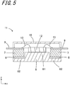
- Fig. 5 is a cross-sectional view of an electronic device.
- An electronic device 11 includes the electronic component mounting package 1 or 1A, the electronic component 12 such as a semiconductor device mounted on the mount area 5, and bonding wires 13, which are connectors that electrically connect the electronic component 12 and the lead terminals 9.
- the electronic device 11 according to the present embodiment is obtained by mounting an intended electronic component 12 on the mount area 5 of the electronic component mounting package 1 or 1A and electrically connecting the mounted electronic component 12 and the lead terminals 9 with the bonding wires 13.
- the electronic component 12 and the heat sink 6 may also be electrically connected with the bonding wires 13.
- the electronic device 11 may also have the heat sink 6 fixed to the surface of a cooling member such as an aluminum block. Heat generated by the electronic component 12 may be transferred through the heat sink 6 and then through the cooling member to be dissipated from the cooling member or transferred to another cooling member.
- the heat sink 6 (electronic component mounting package 1 or 1A) may be fixed to the cooling member with a bond such as the solder described above.
- the heat sink 6 was formed from a copper plate with a thickness of 1 mm punched out in advance into a rectangle (20 mm lengthwise ⁇ 10 mm crosswise).
- the outer periphery (2 mm wide) of the copper plate was pressed to have a thickness of 0.2 mm to form the first portion 61 in the middle portion with a thickness of 1 mm and the second portion 62 in the surrounding portion surrounding the first portion 61.
- the frame 7 formed from sintered alumina (Al 2 O 3 ) was joined to the second portion 62 with a silver brazing material used as the bond 8.
- the lead terminals 9 were then joined to the frame 7 to obtain an electronic component mounting package.
- SIM images for the first and second portions 61 and 62 of the heat sink 6 were obtained through cross-sectional processing with an FIB.
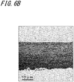
- Fig. 6A is a cross-sectional SIM image of the first portion of the heat sink
- Fig. 6B is a cross-sectional SIM image of the second portion of the heat sink.
- a focused ion beam processing observation system (FB-2100: Hitachi High-Technologies Corporation) was used to perform cross-sectional processing and obtain the SIM images under cross-sectional processing conditions of 40 kV and 4 to 78 nA and the cross-sectional observation condition of 3000 magnifications.
- the obtained SIM images reveal that the crystal grain size of the second portion 62 is smaller in the heat-sink thickness direction than the crystal grain size of the first portion 61.
- the ratio (r2/r1) of the crystal grain size r2 to the crystal grain size r1 in the present example was 0.21.
Landscapes
- Cooling Or The Like Of Semiconductors Or Solid State Devices (AREA)
Abstract
Description
- The present invention relates to an electronic component mounting package for mounting an electronic component, and an electronic device including the package.
- A known electronic component mounting package for mounting an electronic component may include a metal heat sink with an upper surface having a mount area on which an electronic component is mountable, and a frame surrounding the mount area.
- In this electronic component mounting package, the frame and the heat sink are joined with a bond. A semiconductor package described in Patent Literature 1 includes a frame surrounding a raised portion in the middle of a heat sink (flange).
- Patent Literature 1: Japanese Unexamined Patent Application Publication (Translation of PCT Application) No.
2006-516361 - An electronic component mounting package according to one aspect of the present disclosure includes a heat sink, an insulating member, a bond, and an external connection terminal. The heat sink includes a first portion having a mount area on which an electronic component is mountable, and a second portion thinner than the first portion. The heat sink includes a metal. The second portion has a metallic crystal with a crystal grain size smaller than a crystal grain size of a metallic crystal of the first portion in a heat-sink thickness direction. The insulating member is located on the second portion of the heat sink. The insulating member includes ceramic. The bond joins the second portion and the insulating member together. The external connection terminal is electrically insulated from the heat sink with the insulating member.
- An electronic device according to another aspect of the present disclosure includes the electronic component mounting package described above, an electronic component mounted on the mount area, and a connection member to electrically connect the electronic component and the external connection terminal to each other.
- The objects, features, and advantages of the present invention will become apparent from the following detailed description and the drawings.
-
Fig. 1 is a top perspective view of an electronic component mounting package according to an embodiment. -
Fig. 2 is an exploded top perspective view of the electronic component mounting package. -
Fig. 3 is a cross-sectional view of the electronic component mounting package. -
Fig. 4 is a cross-sectional view of an electronic component mounting package according to another embodiment. -
Fig. 5 is a cross-sectional view of an electronic device. -
Fig. 6A is a cross-sectional scanning ion microscope (SIM) image of a first portion of a heat sink. -
Fig. 6B is a cross-sectional SIM image of a second portion of the heat sink. - Embodiments of the present invention will now be described by way of example with reference to the accompanying drawings. Throughout the drawings, an electronic component mounting package and an electronic device are placed on an XY plane defined in a virtual XYZ space. In the present embodiment, the Z-axis direction corresponds to the vertical direction.
-
Fig. 1 is a top perspective view of an electronic component mounting package according to the present embodiment.Fig. 2 is an exploded top perspective view of the electronic component mounting package.Fig. 3 is a cross-sectional view of the electronic component mounting package. An electronic component mounting package 1 according to the present embodiment includes aheat sink 6 having amount area 5 in its middle, on which anelectronic component 12 is mountable, a frame-shaped insulating member (hereafter referred to as a frame) 7 installed on theheat sink 6 to surround themount area 5, abond 8, which joins theheat sink 6 and theframe 7 together, andlead terminals 9 installed on the upper surface of theframe 7 to extend outward from theframe 7. - The
heat sink 6 is formed from a metal, and includes afirst portion 61 including themount area 5, and asecond portion 62 thinner than thefirst portion 61. Theheat sink 6 may be, for example, rectangular or disk-shaped in a plan view. Theheat sink 6 may be rectangular to have a side of 5 to 50 mm, or may be disk-shaped to have a diameter of 5 to 50 mm. Theheat sink 6 is rectangular in the present embodiment. Thefirst portion 61 has a thickness of, for example, 0.5 to 2 mm in the vertical direction. Thesecond portion 62 has a thickness of, for example, 0.1 to 0.5 mm in the vertical direction. Theheat sink 6 has any two portions with different thicknesses. In one example, the rectangularfirst portion 61 and the rectangularsecond portion 62 may be aligned to each other to share one side forming a step. In another example, thesecond portion 62 may be on each side of the rectangularfirst portion 61 and adjacent to the rectangularfirst portion 61. In the present embodiment, thefirst portion 61 is rectangular and located in the middle of theheat sink 6, and thesecond portion 62 surrounds thefirst portion 61. The heat sink 6 as a whole has a rectangular profile. - The
frame 7 is located on the thinsecond portion 62 to surround thefirst portion 61. Theheat sink 6 dissipates heat generated by theelectronic component 12 mounted on themount area 5, and conducts, for example, heat to the back surface of theheat sink 6 to dissipate heat to air or another cooling member. To increase heat dissipation or thermal conductivity, theheat sink 6 may be thick, as thefirst portion 61. To increase joining with theframe 7, theheat sink 6 may be thin, as thesecond portion 62, to reduce warpage or other defects. Theheat sink 6 according to the present embodiment combines the first andsecond portions - In the
heat sink 6 according to the present embodiment, thefirst portion 61 has asurface 61a including themount area 5 and asurface 61b opposite to thesurface 61a, and thesecond portion 62 has asurface 62a on which theframe 7 is installed and asurface 62b opposite to thesurface 62a. Thesurface 61b is flush with thesurface 62b. In other words, theheat sink 6 has a flat back surface without a step. The back surface of theheat sink 6 comes in contact with another cooling member including an aluminum housing to facilitate dissipation. The flat back surface of theheat sink 6 increases the contact area with the cooling member to enhance dissipation efficiency. - In the
heat sink 6 according to the present embodiment, a metallic crystal of thesecond portion 62 has a crystal grain size smaller, in the heat-sink thickness direction, than a crystal grain size of a metallic crystal of thefirst portion 61. A metal having a smaller crystal grain size has higher mechanical strength. In other words, thesecond portion 62 having a smaller crystal grain size in the heat-sink thickness direction has higher strength than thefirst portion 61. In the present embodiment, bonding theframe 7 to thesecond portion 62 having a crystal structure with higher strength enhances the bonding strength between theheat sink 6 and theframe 7 serving as an insulating member. - Examples of the metal used for the
heat sink 6 include a highly thermally conductive material, including a metal such as copper (Cu), silver (Ag), aluminum (Al), or gold (Au) and an alloy of these metals. Copper is used in the present embodiment to increase thermal conductivity and workability, and reduce costs. Examples of copper include pure copper and a variety of copper alloys containing copper as a main component. - The crystal grain size of the metallic crystal of the
heat sink 6 may be measured by any known method, for example, a method for directly measuring the crystal grain size from a cross-sectional image taken parallel to the thickness direction, or an electron backscatter diffraction pattern (EBSD) method. Theheat sink 6 undergoes cross-sectional processing with a focused ion beam (FIB) to obtain a scanning ion microscope (SIM) image as a cross-sectional image with a SIM. The obtained SIM image includes different crystal orientations to allow recognition of crystal grains. The crystal grain size in heat-sink thickness direction is also obtained by, for example, image processing. With the EBSD method, a reflection diffraction pattern is obtained from the surface of a metal sample with a scanning electron microscope (SEM). For example, the crystal orientation can be measured from the reflection diffraction pattern to obtain a crystal orientation map, a crystal grain boundary map, a crystal grain distribution map, and other maps of the metal surface (cross section). The crystal grain size of each of the first andsecond portions heat sink 6 in the heat-sink thickness direction is obtained by measuring the cross section of each of the first andsecond portions second portion 62 is smaller than the crystal grain size of the metallic crystal of thefirst portion 61 in the heat-sink thickness direction. - In this embodiment, r2 < r1, where r1 is the crystal particle grain size of the
first portion 61 in the heat-sink thickness direction, and r2 is the crystal particle grain size of thesecond portion 62 in the heat-sink thickness direction, meaning that the crystal particle grain size of the metallic crystal of thesecond portion 62 is smaller than the crystal particle grain size of the metallic crystal of thefirst portion 61 in the heat-sink thickness direction. The crystal grain size r2 of thesecond portion 62 is smaller than the crystal grain size r1 of thefirst portion 61. For example, the ratio of the crystal grain size r2 to the crystal grain size r1 (r2/r1) falls within the range of 0.05 to 0.5. The crystal grain sizes r1 and r2 are calculated as follows. With the above measuring method, the crystal grain sizes (the largest length in the cross-sectional image in the thickness direction) in the heat-sink thickness direction are measured for 20 pieces in a single cross-sectional area (50 µm lengthwise × 50 µm crosswise), and the arithmetic mean of these values is obtained as an average grain size for the cross section. Similarly, the average grain size for each cross section is calculated for five cross-sectional areas, and the arithmetic mean of these values is obtained. This processing is performed on the first andsecond portions - The
second portion 62 of theheat sink 6 formed from a metal and theframe 7 formed from ceramic are joined together with thebond 8. Thebond 8 may be any material, such as a brazing material, that can join metal and ceramic together. For example, for theheat sink 6 formed from copper, a silver-based brazing material such as a silver brazing material or a Ag-Cu-Sn alloy brazing material is used as thebond 8. Silver in this brazing material diffuses into copper in theheat sink 6, and forms a Ag-Cu alloy. The resultant Ag-Cu alloy has fragility. When the Ag-Cu alloy diffuses in the top layer of theheat sink 6, the alloy easily causes separation or breakage, and lowers the bonding strength. - Other metallic elements in the metal diffuse at a higher speed at the crystal grain boundary than in the crystal grain. The crystal grain boundary can thus be regarded as a diffusion route for these metallic elements. As described above, the
second portion 62 of theheat sink 6 has a small crystal grain size in the heat-sink thickness direction. Thus, thesecond portion 62 substantially has a longer diffusion route, and silver diffusing in copper of theheat sink 6 is more likely to stay at a shallower position. This reduces the likelihood that the Ag-Cu alloy in thesecond portion 62 diffuses and lowers the bonding strength. - The first and
second portions heat sink 6 with different thicknesses may be formed by pressing and/or rolling. Other metal processing such as punching, cutting, etching, and polishing may be performed additionally. For example, a piece having the profile of theheat sink 6 may be punched out from a copper plate, and the peripheral edge may then be pressed or rolled to form the thinsecond portion 62. The metallic crystal in thesecond portion 62 can be plastically deformed by partial pressing or rolling. The crystal grain size of thesecond portion 62 is thus smaller than the crystal grain size of the metallic crystal of thefirst portion 61 in the heat-sink thickness direction. - After punching, the peripheral edge surface has one end portion in the thickness direction having large surface roughness (rough surface portion). When the
second portion 62 has a rough surface portion on thesurface 62a on which theframe 7 is installed, thebond 8 softened to join theframe 7 and theheat sink 6 is less likely to flow outward with the rough surface portion, forming a meniscus near the rough surface portion. Thebond 8 forming a meniscus improves the stress relaxation characteristics, and improves the joining reliability between theframe 7 and theheat sink 6. When thesecond portion 62 has a rough surface portion on thesurface 62b opposite to thesurface 62a on which theframe 7 is installed, the solder softened to join theheat sink 6 and another cooling member such as an aluminum housing is less likely to flow outward with the rough surface portion, forming a meniscus near the rough surface portion. The solder forming a meniscus improves the stress relaxation characteristics, and improves the joining reliability between theheat sink 6 and the cooling member. - The
frame 7 is an insulating member formed from ceramic such as sintered alumina (Al2O3), sintered aluminum nitride (AlN), sintered mullite (3Al2O3, 2SiO2), and glass ceramics, which is selected from materials having a coefficient of thermal expansion approximate to the coefficient of thermal expansion of theheat sink 6. In the present embodiment, theframe 7 is formed from sintered alumina (Al2O3). - For the
frame 7 formed from, for example, sintered alumina, an additive such as an organic binder, a solvent, a plasticizer, or a dispersant is added as appropriate to the powder of a raw material such as alumina, silicon oxide (SiO2), magnesium oxide (MgO), or calcium oxide (CaO), and the mixture of these is then kneaded to obtain slurry. The slurry is then shaped into a sheet using, for example, a doctor blade or by calendering to obtain a ceramic green sheet (ceramic raw sheet). The ceramic green sheet then undergoes punching as appropriate. Multiple ceramic green sheets prepared in this manner are stacked one on another, and are then fired at a temperature of about 1600 °C. - The
lead terminals 9 are strip-shaped external connection terminals formed from a metal such as copper, a copper alloy, an iron-nickel-cobalt alloy, or an iron-nickel alloy. Thelead terminals 9 each have one end in the longitudinal direction connected to theframe 7, and extend outward from theframe 7. Thelead terminals 9 are electrically insulated from theheat sink 6 by theframe 7. Thelead terminals 9 may be located on the upper surface of theframe 7 as in the present embodiment or may extend through theframe 7. -
Fig. 4 is a cross-sectional view of an electronic component mounting package according to another embodiment. An electroniccomponent mounting package 1A according to the present embodiment further includes alid 10. Thelid 10 protects the electronic component mounted on the electroniccomponent mounting package 1A, and provides airtightness and water-tightness inside the package (in the space defined by theframe 7, theheat sink 6, and the lid 10). Thelid 10 may be formed from any material such as ceramics, glass, resin, or a combination of any of these materials. - The
lid 10 may have any shape that allows the package to accommodate an electronic component, such as a flat plate member or a member having a recessed inner surface. Thelid 10 is joined to the upper surface of theframe 7. A bond that joins thelid 10 and theframe 7 may be selected as appropriate in accordance with the material of thelid 10. -
Fig. 5 is a cross-sectional view of an electronic device. Anelectronic device 11 according to the present embodiment includes the electroniccomponent mounting package 1 or 1A, theelectronic component 12 such as a semiconductor device mounted on themount area 5, andbonding wires 13, which are connectors that electrically connect theelectronic component 12 and thelead terminals 9. - The
electronic device 11 according to the present embodiment is obtained by mounting an intendedelectronic component 12 on themount area 5 of the electroniccomponent mounting package 1 or 1A and electrically connecting the mountedelectronic component 12 and thelead terminals 9 with thebonding wires 13. Theelectronic component 12 and theheat sink 6 may also be electrically connected with thebonding wires 13. - The
electronic device 11 may also have theheat sink 6 fixed to the surface of a cooling member such as an aluminum block. Heat generated by theelectronic component 12 may be transferred through theheat sink 6 and then through the cooling member to be dissipated from the cooling member or transferred to another cooling member. The heat sink 6 (electroniccomponent mounting package 1 or 1A) may be fixed to the cooling member with a bond such as the solder described above. - Electronic component mounting packages having the same structure as in the embodiment illustrated in
Figs. 1 to 3 were prepared. Theheat sink 6 was formed from a copper plate with a thickness of 1 mm punched out in advance into a rectangle (20 mm lengthwise × 10 mm crosswise). The outer periphery (2 mm wide) of the copper plate was pressed to have a thickness of 0.2 mm to form thefirst portion 61 in the middle portion with a thickness of 1 mm and thesecond portion 62 in the surrounding portion surrounding thefirst portion 61. Theframe 7 formed from sintered alumina (Al2O3) was joined to thesecond portion 62 with a silver brazing material used as thebond 8. Thelead terminals 9 were then joined to theframe 7 to obtain an electronic component mounting package. - SIM images for the first and
second portions heat sink 6 were obtained through cross-sectional processing with an FIB.Fig. 6A is a cross-sectional SIM image of the first portion of the heat sink, andFig. 6B is a cross-sectional SIM image of the second portion of the heat sink. A focused ion beam processing observation system (FB-2100: Hitachi High-Technologies Corporation) was used to perform cross-sectional processing and obtain the SIM images under cross-sectional processing conditions of 40 kV and 4 to 78 nA and the cross-sectional observation condition of 3000 magnifications. - The obtained SIM images reveal that the crystal grain size of the
second portion 62 is smaller in the heat-sink thickness direction than the crystal grain size of thefirst portion 61. The ratio (r2/r1) of the crystal grain size r2 to the crystal grain size r1 in the present example was 0.21. - The present invention can be embodied in various other forms not departing from the spirit or main features of the invention. The above-described embodiments are thus mere examples in all respects. The scope of the present invention is described in the scope of claims without being restricted to the description. Modifications and changes pertaining to the scope of claims fall within the scope of the present invention.
-
- 1, 1A
- electronic component mounting package
- 5
- mount area
- 6
- heat sink
- 7
- frame
- 8
- bond
- 9
- lead terminal
- 10
- lid
- 11
- electronic device
- 12
- electronic component
- 13
- bonding wire
- 61
- first portion
- 62
- second portion
Claims (6)
- An electronic component mounting package, comprising:a heat sink including a first portion and a second portion thinner than the first portion, the heat sink comprising a metal, the first portion having a mount area on which an electronic component is mountable, the second portion having a metallic crystal with a crystal grain size smaller than a crystal grain size of a metallic crystal of the first portion in a heat-sink thickness direction;an insulating member located on the second portion of the heat sink, the insulating member comprising ceramic;a bond joining the second portion and the insulating member together; andan external connection terminal electrically insulated from the heat sink with the insulating member.
- The electronic component mounting package according to claim 1, wherein
a surface of the first portion of the heat sink opposite to a surface having the mount area is flush with a surface of the second portion of the heat sink opposite to a surface on which the insulating member is located. - The electronic component mounting package according to claim 1 or claim 2, wherein
the metal includes copper. - The electronic component mounting package according to any one of claims 1 to 3, wherein
the first portion is located in a middle of the heat sink, and the second portion surrounds the first portion, and
the insulating member is frame-shaped. - The electronic component mounting package according to claim 4, further comprising:
a lid configured to cover the frame-shaped insulating member. - An electronic device, comprising:the electronic component mounting package according to any one of claims 1 to 5;an electronic component mounted on the mount area; anda connection member to electrically connect the electronic component and the external connection terminal to each other.
Applications Claiming Priority (2)
| Application Number | Priority Date | Filing Date | Title |
|---|---|---|---|
| JP2017162838 | 2017-08-25 | ||
| PCT/JP2018/029486 WO2019039258A1 (en) | 2017-08-25 | 2018-08-06 | Package for electronic component mounting and electronic device |
Publications (2)
| Publication Number | Publication Date |
|---|---|
| EP3675161A1 true EP3675161A1 (en) | 2020-07-01 |
| EP3675161A4 EP3675161A4 (en) | 2021-05-12 |
Family
ID=65438703
Family Applications (1)
| Application Number | Title | Priority Date | Filing Date |
|---|---|---|---|
| EP18847430.8A Withdrawn EP3675161A4 (en) | 2017-08-25 | 2018-08-06 | BOX FOR MOUNTING ELECTRONIC COMPONENTS AND ELECTRONIC DEVICE |
Country Status (4)
| Country | Link |
|---|---|
| US (1) | US20210134687A1 (en) |
| EP (1) | EP3675161A4 (en) |
| JP (1) | JPWO2019039258A1 (en) |
| WO (1) | WO2019039258A1 (en) |
Families Citing this family (2)
| Publication number | Priority date | Publication date | Assignee | Title |
|---|---|---|---|---|
| CN110161726B (en) * | 2019-05-15 | 2022-07-12 | 上海硅酸盐研究所中试基地 | Bridge type crystal radiating block |
| JP7444814B2 (en) * | 2021-04-27 | 2024-03-06 | Ngkエレクトロデバイス株式会社 | package |
Family Cites Families (9)
| Publication number | Priority date | Publication date | Assignee | Title |
|---|---|---|---|---|
| JPH0610695Y2 (en) * | 1987-09-24 | 1994-03-16 | 京セラ株式会社 | Package for storing semiconductor devices |
| JP3493833B2 (en) * | 1995-10-09 | 2004-02-03 | 住友電気工業株式会社 | Plastic package for mounting semiconductor element and method of manufacturing the same |
| JP2001168250A (en) * | 1999-12-10 | 2001-06-22 | Sumitomo Electric Ind Ltd | Semiconductor insulating substrate, semiconductor device using the same, and method of manufacturing the substrate |
| TW461064B (en) * | 2000-12-26 | 2001-10-21 | Siliconware Precision Industries Co Ltd | Thin-type semiconductor device having heat sink structure |
| JP2004235262A (en) * | 2003-01-28 | 2004-08-19 | Kyocera Corp | Semiconductor element storage package and semiconductor device |
| JP3812571B2 (en) * | 2004-03-24 | 2006-08-23 | 松下電器産業株式会社 | Manufacturing method of heat sink for semiconductor device |
| JP2006041287A (en) * | 2004-07-28 | 2006-02-09 | Kyocera Corp | Electronic component storage package and electronic device |
| JP2009277794A (en) * | 2008-05-13 | 2009-11-26 | Sumitomo Metal Electronics Devices Inc | Package for semiconductor element storage |
| JP5271886B2 (en) * | 2009-12-08 | 2013-08-21 | ルネサスエレクトロニクス株式会社 | Semiconductor device and manufacturing method thereof |
-
2018
- 2018-08-06 WO PCT/JP2018/029486 patent/WO2019039258A1/en not_active Ceased
- 2018-08-06 EP EP18847430.8A patent/EP3675161A4/en not_active Withdrawn
- 2018-08-06 JP JP2019538047A patent/JPWO2019039258A1/en active Pending
- 2018-08-06 US US16/641,499 patent/US20210134687A1/en not_active Abandoned
Also Published As
| Publication number | Publication date |
|---|---|
| EP3675161A4 (en) | 2021-05-12 |
| WO2019039258A1 (en) | 2019-02-28 |
| JPWO2019039258A1 (en) | 2020-09-17 |
| US20210134687A1 (en) | 2021-05-06 |
Similar Documents
| Publication | Publication Date | Title |
|---|---|---|
| CN101496165B (en) | Electronic component storing package and electronic device | |
| US9596747B2 (en) | Wiring substrate and electronic device | |
| KR20170044105A (en) | Joined body, substrate for power module provided with heat sink, heat sink, method for manufacturing joined body, method for manufacturing substrate for power module provided with heat sink, and method for manufacturing heat sink | |
| EP3675161A1 (en) | Package for electronic component mounting and electronic device | |
| JPH06296084A (en) | Thermal conductor of high conductivity, wiring board provided therewith and manufacture thereof | |
| CN110313063B (en) | Wiring substrate, package for electronic device, and electronic device | |
| US10943854B2 (en) | Semiconductor package and semiconductor apparatus for use with high-frequency signals and improved heat dissipation | |
| US11778747B2 (en) | Wiring board, composite substrate, and electric device | |
| JP4459031B2 (en) | Electronic component storage package and electronic device | |
| JP2004288949A (en) | Semiconductor element storage package and semiconductor device | |
| JP4227610B2 (en) | Manufacturing method of heat dissipation base | |
| JP6773910B2 (en) | Wiring boards, electronics packages and electronics | |
| US20260114276A1 (en) | Heat dissipation member, heat dissipation member manufacturing method, package, and substrate | |
| JP2005277382A (en) | Electronic component storage package and electronic device | |
| JPH0547953A (en) | Package for semiconductor device | |
| JP2020004801A (en) | Heat sink, semiconductor package, and semiconductor device | |
| JP2009158537A (en) | Package for storing semiconductor elements | |
| JP3872391B2 (en) | Package for storing semiconductor elements | |
| CN1393928A (en) | Sealed encapsulating containing for optical semiconductor device and optical semiconductor module | |
| JP3850312B2 (en) | Semiconductor element storage package and semiconductor device | |
| JP2000114442A (en) | Package for electronic components | |
| JP2006041288A (en) | Electronic component storage package and electronic device | |
| WO2022014411A1 (en) | Substrate for light-emitting element | |
| JP2019041086A (en) | Semiconductor package and semiconductor device | |
| JP2003007940A (en) | Heat radiating member and package for semiconductor element |
Legal Events
| Date | Code | Title | Description |
|---|---|---|---|
| STAA | Information on the status of an ep patent application or granted ep patent |
Free format text: STATUS: THE INTERNATIONAL PUBLICATION HAS BEEN MADE |
|
| PUAI | Public reference made under article 153(3) epc to a published international application that has entered the european phase |
Free format text: ORIGINAL CODE: 0009012 |
|
| STAA | Information on the status of an ep patent application or granted ep patent |
Free format text: STATUS: REQUEST FOR EXAMINATION WAS MADE |
|
| 17P | Request for examination filed |
Effective date: 20200224 |
|
| AK | Designated contracting states |
Kind code of ref document: A1 Designated state(s): AL AT BE BG CH CY CZ DE DK EE ES FI FR GB GR HR HU IE IS IT LI LT LU LV MC MK MT NL NO PL PT RO RS SE SI SK SM TR |
|
| AX | Request for extension of the european patent |
Extension state: BA ME |
|
| DAV | Request for validation of the european patent (deleted) | ||
| DAX | Request for extension of the european patent (deleted) | ||
| A4 | Supplementary search report drawn up and despatched |
Effective date: 20210412 |
|
| RIC1 | Information provided on ipc code assigned before grant |
Ipc: H01L 23/498 20060101ALI20210406BHEP Ipc: H01L 23/367 20060101ALI20210406BHEP Ipc: H01L 23/13 20060101ALI20210406BHEP Ipc: H01L 23/047 20060101AFI20210406BHEP |
|
| STAA | Information on the status of an ep patent application or granted ep patent |
Free format text: STATUS: THE APPLICATION HAS BEEN WITHDRAWN |
|
| 18W | Application withdrawn |
Effective date: 20210813 |