EP3674792A1 - Laminat für eine nichtlineare optik mit einer elektrooptischen polymerschicht und verfahren zu dessen herstellung - Google Patents
Laminat für eine nichtlineare optik mit einer elektrooptischen polymerschicht und verfahren zu dessen herstellung Download PDFInfo
- Publication number
- EP3674792A1 EP3674792A1 EP18848353.1A EP18848353A EP3674792A1 EP 3674792 A1 EP3674792 A1 EP 3674792A1 EP 18848353 A EP18848353 A EP 18848353A EP 3674792 A1 EP3674792 A1 EP 3674792A1
- Authority
- EP
- European Patent Office
- Prior art keywords
- electro
- optic polymer
- optic
- polymer layer
- laminate
- Prior art date
- Legal status (The legal status is an assumption and is not a legal conclusion. Google has not performed a legal analysis and makes no representation as to the accuracy of the status listed.)
- Pending
Links
- 229920000642 polymer Polymers 0.000 title claims abstract description 322
- 238000004519 manufacturing process Methods 0.000 title claims abstract description 26
- 238000012545 processing Methods 0.000 claims abstract description 130
- 238000010030 laminating Methods 0.000 claims abstract description 27
- 230000003287 optical effect Effects 0.000 claims description 71
- 238000000034 method Methods 0.000 claims description 65
- -1 polyethylene Polymers 0.000 claims description 42
- 229920001577 copolymer Polymers 0.000 claims description 29
- 229920000089 Cyclic olefin copolymer Polymers 0.000 claims description 26
- 239000000203 mixture Substances 0.000 claims description 20
- VYPSYNLAJGMNEJ-UHFFFAOYSA-N Silicium dioxide Chemical compound O=[Si]=O VYPSYNLAJGMNEJ-UHFFFAOYSA-N 0.000 claims description 17
- XLOMVQKBTHCTTD-UHFFFAOYSA-N Zinc monoxide Chemical compound [Zn]=O XLOMVQKBTHCTTD-UHFFFAOYSA-N 0.000 claims description 15
- XUIMIQQOPSSXEZ-UHFFFAOYSA-N Silicon Chemical compound [Si] XUIMIQQOPSSXEZ-UHFFFAOYSA-N 0.000 claims description 14
- 229910052710 silicon Inorganic materials 0.000 claims description 14
- 239000010703 silicon Substances 0.000 claims description 14
- 239000011521 glass Substances 0.000 claims description 13
- 239000011347 resin Substances 0.000 claims description 13
- 229920005989 resin Polymers 0.000 claims description 13
- 239000004372 Polyvinyl alcohol Substances 0.000 claims description 9
- 239000000853 adhesive Substances 0.000 claims description 9
- 230000001070 adhesive effect Effects 0.000 claims description 9
- 229920002451 polyvinyl alcohol Polymers 0.000 claims description 9
- 239000000377 silicon dioxide Substances 0.000 claims description 7
- 239000011787 zinc oxide Substances 0.000 claims description 7
- 239000004698 Polyethylene Substances 0.000 claims description 6
- 239000004642 Polyimide Substances 0.000 claims description 6
- 239000004743 Polypropylene Substances 0.000 claims description 6
- 239000004793 Polystyrene Substances 0.000 claims description 6
- TWNQGVIAIRXVLR-UHFFFAOYSA-N oxo(oxoalumanyloxy)alumane Chemical compound O=[Al]O[Al]=O TWNQGVIAIRXVLR-UHFFFAOYSA-N 0.000 claims description 6
- 239000004417 polycarbonate Substances 0.000 claims description 6
- 229920000515 polycarbonate Polymers 0.000 claims description 6
- 229920000573 polyethylene Polymers 0.000 claims description 6
- 229920000139 polyethylene terephthalate Polymers 0.000 claims description 6
- 239000005020 polyethylene terephthalate Substances 0.000 claims description 6
- 229920001721 polyimide Polymers 0.000 claims description 6
- 229920000306 polymethylpentene Polymers 0.000 claims description 6
- 239000011116 polymethylpentene Substances 0.000 claims description 6
- 229920001155 polypropylene Polymers 0.000 claims description 6
- 229920002223 polystyrene Polymers 0.000 claims description 6
- JBRZTFJDHDCESZ-UHFFFAOYSA-N AsGa Chemical compound [As]#[Ga] JBRZTFJDHDCESZ-UHFFFAOYSA-N 0.000 claims description 5
- GPXJNWSHGFTCBW-UHFFFAOYSA-N Indium phosphide Chemical compound [In]#P GPXJNWSHGFTCBW-UHFFFAOYSA-N 0.000 claims description 5
- 229910052581 Si3N4 Inorganic materials 0.000 claims description 5
- GWEVSGVZZGPLCZ-UHFFFAOYSA-N Titan oxide Chemical compound O=[Ti]=O GWEVSGVZZGPLCZ-UHFFFAOYSA-N 0.000 claims description 5
- 230000003993 interaction Effects 0.000 claims description 5
- 229920000058 polyacrylate Polymers 0.000 claims description 5
- HQVNEWCFYHHQES-UHFFFAOYSA-N silicon nitride Chemical compound N12[Si]34N5[Si]62N3[Si]51N64 HQVNEWCFYHHQES-UHFFFAOYSA-N 0.000 claims description 5
- 229910001218 Gallium arsenide Inorganic materials 0.000 claims description 4
- PMHQVHHXPFUNSP-UHFFFAOYSA-M copper(1+);methylsulfanylmethane;bromide Chemical compound Br[Cu].CSC PMHQVHHXPFUNSP-UHFFFAOYSA-M 0.000 claims description 4
- OGIDPMRJRNCKJF-UHFFFAOYSA-N titanium oxide Inorganic materials [Ti]=O OGIDPMRJRNCKJF-UHFFFAOYSA-N 0.000 claims description 4
- 230000009881 electrostatic interaction Effects 0.000 claims description 3
- 229910052681 coesite Inorganic materials 0.000 claims 1
- 229910052906 cristobalite Inorganic materials 0.000 claims 1
- 229910052682 stishovite Inorganic materials 0.000 claims 1
- 229910052905 tridymite Inorganic materials 0.000 claims 1
- 239000010410 layer Substances 0.000 description 245
- 239000000463 material Substances 0.000 description 50
- 239000000523 sample Substances 0.000 description 47
- 239000010409 thin film Substances 0.000 description 22
- 238000010521 absorption reaction Methods 0.000 description 19
- 229920006254 polymer film Polymers 0.000 description 16
- QVGXLLKOCUKJST-UHFFFAOYSA-N atomic oxygen Chemical compound [O] QVGXLLKOCUKJST-UHFFFAOYSA-N 0.000 description 15
- 229910052760 oxygen Inorganic materials 0.000 description 15
- 239000001301 oxygen Substances 0.000 description 15
- 238000001228 spectrum Methods 0.000 description 15
- 229920005601 base polymer Polymers 0.000 description 14
- 239000000758 substrate Substances 0.000 description 14
- 239000010408 film Substances 0.000 description 13
- 239000011159 matrix material Substances 0.000 description 13
- 238000000862 absorption spectrum Methods 0.000 description 12
- 239000012792 core layer Substances 0.000 description 12
- 238000001020 plasma etching Methods 0.000 description 12
- 239000006087 Silane Coupling Agent Substances 0.000 description 11
- 125000003277 amino group Chemical group 0.000 description 10
- 150000001875 compounds Chemical class 0.000 description 10
- 230000000694 effects Effects 0.000 description 9
- 229920003229 poly(methyl methacrylate) Polymers 0.000 description 9
- 239000004926 polymethyl methacrylate Substances 0.000 description 9
- CERQOIWHTDAKMF-UHFFFAOYSA-M Methacrylate Chemical compound CC(=C)C([O-])=O CERQOIWHTDAKMF-UHFFFAOYSA-M 0.000 description 8
- JRZJOMJEPLMPRA-UHFFFAOYSA-N olefin Natural products CCCCCCCC=C JRZJOMJEPLMPRA-UHFFFAOYSA-N 0.000 description 8
- 229910052751 metal Inorganic materials 0.000 description 7
- 239000002184 metal Substances 0.000 description 7
- 238000002360 preparation method Methods 0.000 description 7
- 238000004528 spin coating Methods 0.000 description 7
- 239000000126 substance Substances 0.000 description 7
- IISBACLAFKSPIT-UHFFFAOYSA-N bisphenol A Chemical compound C=1C=C(O)C=CC=1C(C)(C)C1=CC=C(O)C=C1 IISBACLAFKSPIT-UHFFFAOYSA-N 0.000 description 6
- 238000006243 chemical reaction Methods 0.000 description 6
- 238000001312 dry etching Methods 0.000 description 6
- 230000005684 electric field Effects 0.000 description 6
- 238000001000 micrograph Methods 0.000 description 6
- SKJCKYVIQGBWTN-UHFFFAOYSA-N (4-hydroxyphenyl) methanesulfonate Chemical compound CS(=O)(=O)OC1=CC=C(O)C=C1 SKJCKYVIQGBWTN-UHFFFAOYSA-N 0.000 description 5
- WKBPZYKAUNRMKP-UHFFFAOYSA-N 1-[2-(2,4-dichlorophenyl)pentyl]1,2,4-triazole Chemical compound C=1C=C(Cl)C=C(Cl)C=1C(CCC)CN1C=NC=N1 WKBPZYKAUNRMKP-UHFFFAOYSA-N 0.000 description 5
- 238000007796 conventional method Methods 0.000 description 5
- 150000001925 cycloalkenes Chemical class 0.000 description 5
- 230000009477 glass transition Effects 0.000 description 5
- 238000000206 photolithography Methods 0.000 description 5
- 239000004065 semiconductor Substances 0.000 description 5
- PFNQVRZLDWYSCW-UHFFFAOYSA-N (fluoren-9-ylideneamino) n-naphthalen-1-ylcarbamate Chemical compound C12=CC=CC=C2C2=CC=CC=C2C1=NOC(=O)NC1=CC=CC2=CC=CC=C12 PFNQVRZLDWYSCW-UHFFFAOYSA-N 0.000 description 4
- FEJPWLNPOFOBSP-UHFFFAOYSA-N 2-[4-[(2-chloro-4-nitrophenyl)diazenyl]-n-ethylanilino]ethanol Chemical compound C1=CC(N(CCO)CC)=CC=C1N=NC1=CC=C([N+]([O-])=O)C=C1Cl FEJPWLNPOFOBSP-UHFFFAOYSA-N 0.000 description 4
- 230000008859 change Effects 0.000 description 4
- 230000010287 polarization Effects 0.000 description 4
- 230000008569 process Effects 0.000 description 4
- NIXOWILDQLNWCW-UHFFFAOYSA-M Acrylate Chemical compound [O-]C(=O)C=C NIXOWILDQLNWCW-UHFFFAOYSA-M 0.000 description 3
- UHOVQNZJYSORNB-UHFFFAOYSA-N Benzene Chemical compound C1=CC=CC=C1 UHOVQNZJYSORNB-UHFFFAOYSA-N 0.000 description 3
- 230000005697 Pockels effect Effects 0.000 description 3
- 150000001336 alkenes Chemical class 0.000 description 3
- 229910052782 aluminium Inorganic materials 0.000 description 3
- XAGFODPZIPBFFR-UHFFFAOYSA-N aluminium Chemical compound [Al] XAGFODPZIPBFFR-UHFFFAOYSA-N 0.000 description 3
- 101150059062 apln gene Proteins 0.000 description 3
- 230000005540 biological transmission Effects 0.000 description 3
- 239000004020 conductor Substances 0.000 description 3
- 230000003247 decreasing effect Effects 0.000 description 3
- 238000000572 ellipsometry Methods 0.000 description 3
- 239000010931 gold Substances 0.000 description 3
- 229910052735 hafnium Inorganic materials 0.000 description 3
- RAXXELZNTBOGNW-UHFFFAOYSA-N imidazole Natural products C1=CNC=N1 RAXXELZNTBOGNW-UHFFFAOYSA-N 0.000 description 3
- 238000003475 lamination Methods 0.000 description 3
- 150000004767 nitrides Chemical class 0.000 description 3
- 229920000620 organic polymer Polymers 0.000 description 3
- BASFCYQUMIYNBI-UHFFFAOYSA-N platinum Chemical compound [Pt] BASFCYQUMIYNBI-UHFFFAOYSA-N 0.000 description 3
- 229920005604 random copolymer Polymers 0.000 description 3
- 238000004544 sputter deposition Methods 0.000 description 3
- XOLBLPGZBRYERU-UHFFFAOYSA-N tin dioxide Chemical compound O=[Sn]=O XOLBLPGZBRYERU-UHFFFAOYSA-N 0.000 description 3
- 238000001039 wet etching Methods 0.000 description 3
- LIKMAJRDDDTEIG-UHFFFAOYSA-N 1-hexene Chemical compound CCCCC=C LIKMAJRDDDTEIG-UHFFFAOYSA-N 0.000 description 2
- KWKAKUADMBZCLK-UHFFFAOYSA-N 1-octene Chemical compound CCCCCCC=C KWKAKUADMBZCLK-UHFFFAOYSA-N 0.000 description 2
- YBYIRNPNPLQARY-UHFFFAOYSA-N 1H-indene Chemical compound C1=CC=C2CC=CC2=C1 YBYIRNPNPLQARY-UHFFFAOYSA-N 0.000 description 2
- WUPHOULIZUERAE-UHFFFAOYSA-N 3-(oxolan-2-yl)propanoic acid Chemical compound OC(=O)CCC1CCCO1 WUPHOULIZUERAE-UHFFFAOYSA-N 0.000 description 2
- YLQBMQCUIZJEEH-UHFFFAOYSA-N Furan Chemical compound C=1C=COC=1 YLQBMQCUIZJEEH-UHFFFAOYSA-N 0.000 description 2
- VQTUBCCKSQIDNK-UHFFFAOYSA-N Isobutene Chemical compound CC(C)=C VQTUBCCKSQIDNK-UHFFFAOYSA-N 0.000 description 2
- UFWIBTONFRDIAS-UHFFFAOYSA-N Naphthalene Chemical compound C1=CC=CC2=CC=CC=C21 UFWIBTONFRDIAS-UHFFFAOYSA-N 0.000 description 2
- KYQCOXFCLRTKLS-UHFFFAOYSA-N Pyrazine Chemical compound C1=CN=CC=N1 KYQCOXFCLRTKLS-UHFFFAOYSA-N 0.000 description 2
- JUJWROOIHBZHMG-UHFFFAOYSA-N Pyridine Chemical compound C1=CC=NC=C1 JUJWROOIHBZHMG-UHFFFAOYSA-N 0.000 description 2
- KAESVJOAVNADME-UHFFFAOYSA-N Pyrrole Chemical compound C=1C=CNC=1 KAESVJOAVNADME-UHFFFAOYSA-N 0.000 description 2
- SMWDFEZZVXVKRB-UHFFFAOYSA-N Quinoline Chemical compound N1=CC=CC2=CC=CC=C21 SMWDFEZZVXVKRB-UHFFFAOYSA-N 0.000 description 2
- 229910000577 Silicon-germanium Inorganic materials 0.000 description 2
- BQCADISMDOOEFD-UHFFFAOYSA-N Silver Chemical compound [Ag] BQCADISMDOOEFD-UHFFFAOYSA-N 0.000 description 2
- 239000004809 Teflon Substances 0.000 description 2
- 229920006362 Teflon® Polymers 0.000 description 2
- YTPLMLYBLZKORZ-UHFFFAOYSA-N Thiophene Chemical compound C=1C=CSC=1 YTPLMLYBLZKORZ-UHFFFAOYSA-N 0.000 description 2
- 239000005083 Zinc sulfide Substances 0.000 description 2
- MCMNRKCIXSYSNV-UHFFFAOYSA-N ZrO2 Inorganic materials O=[Zr]=O MCMNRKCIXSYSNV-UHFFFAOYSA-N 0.000 description 2
- 230000003321 amplification Effects 0.000 description 2
- MWPLVEDNUUSJAV-UHFFFAOYSA-N anthracene Chemical compound C1=CC=CC2=CC3=CC=CC=C3C=C21 MWPLVEDNUUSJAV-UHFFFAOYSA-N 0.000 description 2
- 229920001400 block copolymer Polymers 0.000 description 2
- 229910052980 cadmium sulfide Inorganic materials 0.000 description 2
- QWUZMTJBRUASOW-UHFFFAOYSA-N cadmium tellanylidenezinc Chemical compound [Zn].[Cd].[Te] QWUZMTJBRUASOW-UHFFFAOYSA-N 0.000 description 2
- 125000002915 carbonyl group Chemical group [*:2]C([*:1])=O 0.000 description 2
- 230000015556 catabolic process Effects 0.000 description 2
- 238000000576 coating method Methods 0.000 description 2
- 238000004891 communication Methods 0.000 description 2
- 239000010949 copper Substances 0.000 description 2
- 239000013078 crystal Substances 0.000 description 2
- LPIQUOYDBNQMRZ-UHFFFAOYSA-N cyclopentene Chemical compound C1CC=CC1 LPIQUOYDBNQMRZ-UHFFFAOYSA-N 0.000 description 2
- ZUOUZKKEUPVFJK-UHFFFAOYSA-N diphenyl Chemical compound C1=CC=CC=C1C1=CC=CC=C1 ZUOUZKKEUPVFJK-UHFFFAOYSA-N 0.000 description 2
- 125000006575 electron-withdrawing group Chemical group 0.000 description 2
- PCHJSUWPFVWCPO-UHFFFAOYSA-N gold Chemical compound [Au] PCHJSUWPFVWCPO-UHFFFAOYSA-N 0.000 description 2
- 229910052737 gold Inorganic materials 0.000 description 2
- 229920000578 graft copolymer Polymers 0.000 description 2
- VBJZVLUMGGDVMO-UHFFFAOYSA-N hafnium atom Chemical compound [Hf] VBJZVLUMGGDVMO-UHFFFAOYSA-N 0.000 description 2
- AMGQUBHHOARCQH-UHFFFAOYSA-N indium;oxotin Chemical compound [In].[Sn]=O AMGQUBHHOARCQH-UHFFFAOYSA-N 0.000 description 2
- GQYHUHYESMUTHG-UHFFFAOYSA-N lithium niobate Chemical compound [Li+].[O-][Nb](=O)=O GQYHUHYESMUTHG-UHFFFAOYSA-N 0.000 description 2
- 239000000395 magnesium oxide Substances 0.000 description 2
- CPLXHLVBOLITMK-UHFFFAOYSA-N magnesium oxide Inorganic materials [Mg]=O CPLXHLVBOLITMK-UHFFFAOYSA-N 0.000 description 2
- AXZKOIWUVFPNLO-UHFFFAOYSA-N magnesium;oxygen(2-) Chemical compound [O-2].[Mg+2] AXZKOIWUVFPNLO-UHFFFAOYSA-N 0.000 description 2
- 238000002156 mixing Methods 0.000 description 2
- JFNLZVQOOSMTJK-KNVOCYPGSA-N norbornene Chemical compound C1[C@@H]2CC[C@H]1C=C2 JFNLZVQOOSMTJK-KNVOCYPGSA-N 0.000 description 2
- 238000003199 nucleic acid amplification method Methods 0.000 description 2
- 239000011368 organic material Substances 0.000 description 2
- 230000010355 oscillation Effects 0.000 description 2
- SIWVEOZUMHYXCS-UHFFFAOYSA-N oxo(oxoyttriooxy)yttrium Chemical compound O=[Y]O[Y]=O SIWVEOZUMHYXCS-UHFFFAOYSA-N 0.000 description 2
- BPUBBGLMJRNUCC-UHFFFAOYSA-N oxygen(2-);tantalum(5+) Chemical compound [O-2].[O-2].[O-2].[O-2].[O-2].[Ta+5].[Ta+5] BPUBBGLMJRNUCC-UHFFFAOYSA-N 0.000 description 2
- RVTZCBVAJQQJTK-UHFFFAOYSA-N oxygen(2-);zirconium(4+) Chemical compound [O-2].[O-2].[Zr+4] RVTZCBVAJQQJTK-UHFFFAOYSA-N 0.000 description 2
- NRNCYVBFPDDJNE-UHFFFAOYSA-N pemoline Chemical compound O1C(N)=NC(=O)C1C1=CC=CC=C1 NRNCYVBFPDDJNE-UHFFFAOYSA-N 0.000 description 2
- YWAKXRMUMFPDSH-UHFFFAOYSA-N pentene Chemical compound CCCC=C YWAKXRMUMFPDSH-UHFFFAOYSA-N 0.000 description 2
- 229920000098 polyolefin Polymers 0.000 description 2
- 229920001343 polytetrafluoroethylene Polymers 0.000 description 2
- 239000004810 polytetrafluoroethylene Substances 0.000 description 2
- 238000005070 sampling Methods 0.000 description 2
- 229910052709 silver Inorganic materials 0.000 description 2
- 239000004332 silver Substances 0.000 description 2
- 239000000243 solution Substances 0.000 description 2
- 125000001424 substituent group Chemical group 0.000 description 2
- PBCFLUZVCVVTBY-UHFFFAOYSA-N tantalum pentoxide Inorganic materials O=[Ta](=O)O[Ta](=O)=O PBCFLUZVCVVTBY-UHFFFAOYSA-N 0.000 description 2
- YVTHLONGBIQYBO-UHFFFAOYSA-N zinc indium(3+) oxygen(2-) Chemical compound [O--].[Zn++].[In+3] YVTHLONGBIQYBO-UHFFFAOYSA-N 0.000 description 2
- 229910052984 zinc sulfide Inorganic materials 0.000 description 2
- HECLRDQVFMWTQS-RGOKHQFPSA-N 1755-01-7 Chemical compound C1[C@H]2[C@@H]3CC=C[C@@H]3[C@@H]1C=C2 HECLRDQVFMWTQS-RGOKHQFPSA-N 0.000 description 1
- MGADZUXDNSDTHW-UHFFFAOYSA-N 2H-pyran Chemical compound C1OC=CC=C1 MGADZUXDNSDTHW-UHFFFAOYSA-N 0.000 description 1
- GOLORTLGFDVFDW-UHFFFAOYSA-N 3-(1h-benzimidazol-2-yl)-7-(diethylamino)chromen-2-one Chemical compound C1=CC=C2NC(C3=CC4=CC=C(C=C4OC3=O)N(CC)CC)=NC2=C1 GOLORTLGFDVFDW-UHFFFAOYSA-N 0.000 description 1
- LDTAOIUHUHHCMU-UHFFFAOYSA-N 3-methylpent-1-ene Chemical compound CCC(C)C=C LDTAOIUHUHHCMU-UHFFFAOYSA-N 0.000 description 1
- WSMQKESQZFQMFW-UHFFFAOYSA-N 5-methyl-pyrazole-3-carboxylic acid Chemical compound CC1=CC(C(O)=O)=NN1 WSMQKESQZFQMFW-UHFFFAOYSA-N 0.000 description 1
- PIGFYZPCRLYGLF-UHFFFAOYSA-N Aluminum nitride Chemical compound [Al]#N PIGFYZPCRLYGLF-UHFFFAOYSA-N 0.000 description 1
- VYZAMTAEIAYCRO-UHFFFAOYSA-N Chromium Chemical compound [Cr] VYZAMTAEIAYCRO-UHFFFAOYSA-N 0.000 description 1
- RYGMFSIKBFXOCR-UHFFFAOYSA-N Copper Chemical compound [Cu] RYGMFSIKBFXOCR-UHFFFAOYSA-N 0.000 description 1
- JMASRVWKEDWRBT-UHFFFAOYSA-N Gallium nitride Chemical compound [Ga]#N JMASRVWKEDWRBT-UHFFFAOYSA-N 0.000 description 1
- 229910003327 LiNbO3 Inorganic materials 0.000 description 1
- BPQQTUXANYXVAA-UHFFFAOYSA-N Orthosilicate Chemical compound [O-][Si]([O-])([O-])[O-] BPQQTUXANYXVAA-UHFFFAOYSA-N 0.000 description 1
- PCNDJXKNXGMECE-UHFFFAOYSA-N Phenazine Natural products C1=CC=CC2=NC3=CC=CC=C3N=C21 PCNDJXKNXGMECE-UHFFFAOYSA-N 0.000 description 1
- 239000004952 Polyamide Substances 0.000 description 1
- 239000004695 Polyether sulfone Substances 0.000 description 1
- 239000004734 Polyphenylene sulfide Substances 0.000 description 1
- 229920002396 Polyurea Polymers 0.000 description 1
- WTKZEGDFNFYCGP-UHFFFAOYSA-N Pyrazole Chemical compound C=1C=NNC=1 WTKZEGDFNFYCGP-UHFFFAOYSA-N 0.000 description 1
- CZPWVGJYEJSRLH-UHFFFAOYSA-N Pyrimidine Chemical compound C1=CN=CN=C1 CZPWVGJYEJSRLH-UHFFFAOYSA-N 0.000 description 1
- BLRPTPMANUNPDV-UHFFFAOYSA-N Silane Chemical compound [SiH4] BLRPTPMANUNPDV-UHFFFAOYSA-N 0.000 description 1
- PJANXHGTPQOBST-VAWYXSNFSA-N Stilbene Natural products C=1C=CC=CC=1/C=C/C1=CC=CC=C1 PJANXHGTPQOBST-VAWYXSNFSA-N 0.000 description 1
- FZWLAAWBMGSTSO-UHFFFAOYSA-N Thiazole Chemical compound C1=CSC=N1 FZWLAAWBMGSTSO-UHFFFAOYSA-N 0.000 description 1
- RTAQQCXQSZGOHL-UHFFFAOYSA-N Titanium Chemical compound [Ti] RTAQQCXQSZGOHL-UHFFFAOYSA-N 0.000 description 1
- NRTOMJZYCJJWKI-UHFFFAOYSA-N Titanium nitride Chemical compound [Ti]#N NRTOMJZYCJJWKI-UHFFFAOYSA-N 0.000 description 1
- LEVVHYCKPQWKOP-UHFFFAOYSA-N [Si].[Ge] Chemical compound [Si].[Ge] LEVVHYCKPQWKOP-UHFFFAOYSA-N 0.000 description 1
- 125000002252 acyl group Chemical group 0.000 description 1
- 125000003545 alkoxy group Chemical group 0.000 description 1
- 125000000217 alkyl group Chemical group 0.000 description 1
- 125000005336 allyloxy group Chemical group 0.000 description 1
- XKMRRTOUMJRJIA-UHFFFAOYSA-N ammonia nh3 Chemical compound N.N XKMRRTOUMJRJIA-UHFFFAOYSA-N 0.000 description 1
- 150000001491 aromatic compounds Chemical class 0.000 description 1
- 125000003118 aryl group Chemical group 0.000 description 1
- 238000007611 bar coating method Methods 0.000 description 1
- 230000004888 barrier function Effects 0.000 description 1
- 235000010290 biphenyl Nutrition 0.000 description 1
- 239000004305 biphenyl Substances 0.000 description 1
- 229910052793 cadmium Inorganic materials 0.000 description 1
- BDOSMKKIYDKNTQ-UHFFFAOYSA-N cadmium atom Chemical compound [Cd] BDOSMKKIYDKNTQ-UHFFFAOYSA-N 0.000 description 1
- AQCDIIAORKRFCD-UHFFFAOYSA-N cadmium selenide Chemical compound [Cd]=[Se] AQCDIIAORKRFCD-UHFFFAOYSA-N 0.000 description 1
- 125000001951 carbamoylamino group Chemical group C(N)(=O)N* 0.000 description 1
- CREMABGTGYGIQB-UHFFFAOYSA-N carbon carbon Chemical compound C.C CREMABGTGYGIQB-UHFFFAOYSA-N 0.000 description 1
- 239000011203 carbon fibre reinforced carbon Substances 0.000 description 1
- 239000003153 chemical reaction reagent Substances 0.000 description 1
- 229910052804 chromium Inorganic materials 0.000 description 1
- 239000011651 chromium Substances 0.000 description 1
- 239000000470 constituent Substances 0.000 description 1
- 238000010276 construction Methods 0.000 description 1
- 229910052802 copper Inorganic materials 0.000 description 1
- 230000008878 coupling Effects 0.000 description 1
- 238000010168 coupling process Methods 0.000 description 1
- 238000005859 coupling reaction Methods 0.000 description 1
- 125000004093 cyano group Chemical group *C#N 0.000 description 1
- 125000004122 cyclic group Chemical group 0.000 description 1
- CFBGXYDUODCMNS-UHFFFAOYSA-N cyclobutene Chemical compound C1CC=C1 CFBGXYDUODCMNS-UHFFFAOYSA-N 0.000 description 1
- ZXIJMRYMVAMXQP-UHFFFAOYSA-N cycloheptene Chemical compound C1CCC=CCC1 ZXIJMRYMVAMXQP-UHFFFAOYSA-N 0.000 description 1
- URYYVOIYTNXXBN-UPHRSURJSA-N cyclooctene Chemical compound C1CCC\C=C/CC1 URYYVOIYTNXXBN-UPHRSURJSA-N 0.000 description 1
- 239000004913 cyclooctene Substances 0.000 description 1
- 238000013461 design Methods 0.000 description 1
- 238000001514 detection method Methods 0.000 description 1
- 239000010432 diamond Substances 0.000 description 1
- 229910003460 diamond Inorganic materials 0.000 description 1
- CSJLBAMHHLJAAS-UHFFFAOYSA-N diethylaminosulfur trifluoride Substances CCN(CC)S(F)(F)F CSJLBAMHHLJAAS-UHFFFAOYSA-N 0.000 description 1
- AJNVQOSZGJRYEI-UHFFFAOYSA-N digallium;oxygen(2-) Chemical compound [O-2].[O-2].[O-2].[Ga+3].[Ga+3] AJNVQOSZGJRYEI-UHFFFAOYSA-N 0.000 description 1
- 238000003618 dip coating Methods 0.000 description 1
- 229920006332 epoxy adhesive Polymers 0.000 description 1
- 125000003700 epoxy group Chemical group 0.000 description 1
- 239000003822 epoxy resin Substances 0.000 description 1
- 238000011156 evaluation Methods 0.000 description 1
- 230000001747 exhibiting effect Effects 0.000 description 1
- HZXMRANICFIONG-UHFFFAOYSA-N gallium phosphide Chemical compound [Ga]#P HZXMRANICFIONG-UHFFFAOYSA-N 0.000 description 1
- 229910052732 germanium Inorganic materials 0.000 description 1
- GNPVGFCGXDBREM-UHFFFAOYSA-N germanium atom Chemical compound [Ge] GNPVGFCGXDBREM-UHFFFAOYSA-N 0.000 description 1
- 238000007756 gravure coating Methods 0.000 description 1
- CJNBYAVZURUTKZ-UHFFFAOYSA-N hafnium(iv) oxide Chemical compound O=[Hf]=O CJNBYAVZURUTKZ-UHFFFAOYSA-N 0.000 description 1
- 229910000167 hafnon Inorganic materials 0.000 description 1
- 125000005843 halogen group Chemical group 0.000 description 1
- 238000010438 heat treatment Methods 0.000 description 1
- 150000002391 heterocyclic compounds Chemical class 0.000 description 1
- 238000002347 injection Methods 0.000 description 1
- 239000007924 injection Substances 0.000 description 1
- 230000001678 irradiating effect Effects 0.000 description 1
- IQPQWNKOIGAROB-UHFFFAOYSA-N isocyanate group Chemical group [N-]=C=O IQPQWNKOIGAROB-UHFFFAOYSA-N 0.000 description 1
- ZFSLODLOARCGLH-UHFFFAOYSA-N isocyanuric acid Chemical group OC1=NC(O)=NC(O)=N1 ZFSLODLOARCGLH-UHFFFAOYSA-N 0.000 description 1
- MRELNEQAGSRDBK-UHFFFAOYSA-N lanthanum(3+);oxygen(2-) Chemical compound [O-2].[O-2].[O-2].[La+3].[La+3] MRELNEQAGSRDBK-UHFFFAOYSA-N 0.000 description 1
- HFGPZNIAWCZYJU-UHFFFAOYSA-N lead zirconate titanate Chemical compound [O-2].[O-2].[O-2].[O-2].[O-2].[Ti+4].[Zr+4].[Pb+2] HFGPZNIAWCZYJU-UHFFFAOYSA-N 0.000 description 1
- 229910052451 lead zirconate titanate Inorganic materials 0.000 description 1
- 229910044991 metal oxide Inorganic materials 0.000 description 1
- 150000004706 metal oxides Chemical class 0.000 description 1
- 125000005641 methacryl group Chemical group 0.000 description 1
- 238000012986 modification Methods 0.000 description 1
- 230000004048 modification Effects 0.000 description 1
- TVMXDCGIABBOFY-UHFFFAOYSA-N n-Octanol Natural products CCCCCCCC TVMXDCGIABBOFY-UHFFFAOYSA-N 0.000 description 1
- 125000000449 nitro group Chemical group [O-][N+](*)=O 0.000 description 1
- 125000000962 organic group Chemical group 0.000 description 1
- JMANVNJQNLATNU-UHFFFAOYSA-N oxalonitrile Chemical compound N#CC#N JMANVNJQNLATNU-UHFFFAOYSA-N 0.000 description 1
- RGSFGYAAUTVSQA-UHFFFAOYSA-N pentamethylene Natural products C1CCCC1 RGSFGYAAUTVSQA-UHFFFAOYSA-N 0.000 description 1
- 125000005010 perfluoroalkyl group Chemical group 0.000 description 1
- 125000002080 perylenyl group Chemical group C1(=CC=C2C=CC=C3C4=CC=CC5=CC=CC(C1=C23)=C45)* 0.000 description 1
- CSHWQDPOILHKBI-UHFFFAOYSA-N peryrene Natural products C1=CC(C2=CC=CC=3C2=C2C=CC=3)=C3C2=CC=CC3=C1 CSHWQDPOILHKBI-UHFFFAOYSA-N 0.000 description 1
- 229910052697 platinum Inorganic materials 0.000 description 1
- 229920000636 poly(norbornene) polymer Polymers 0.000 description 1
- 229920002492 poly(sulfone) Polymers 0.000 description 1
- 229920002647 polyamide Polymers 0.000 description 1
- 229920000647 polyepoxide Polymers 0.000 description 1
- 229920000728 polyester Polymers 0.000 description 1
- 229920006393 polyether sulfone Polymers 0.000 description 1
- 229920000069 polyphenylene sulfide Polymers 0.000 description 1
- PBMFSQRYOILNGV-UHFFFAOYSA-N pyridazine Chemical compound C1=CC=NN=C1 PBMFSQRYOILNGV-UHFFFAOYSA-N 0.000 description 1
- UMJSCPRVCHMLSP-UHFFFAOYSA-N pyridine Natural products COC1=CC=CN=C1 UMJSCPRVCHMLSP-UHFFFAOYSA-N 0.000 description 1
- 238000011160 research Methods 0.000 description 1
- 229910000077 silane Inorganic materials 0.000 description 1
- HBMJWWWQQXIZIP-UHFFFAOYSA-N silicon carbide Chemical compound [Si+]#[C-] HBMJWWWQQXIZIP-UHFFFAOYSA-N 0.000 description 1
- 235000012239 silicon dioxide Nutrition 0.000 description 1
- 229910052814 silicon oxide Inorganic materials 0.000 description 1
- 238000004088 simulation Methods 0.000 description 1
- 239000002356 single layer Substances 0.000 description 1
- 238000005507 spraying Methods 0.000 description 1
- PJANXHGTPQOBST-UHFFFAOYSA-N stilbene Chemical compound C=1C=CC=CC=1C=CC1=CC=CC=C1 PJANXHGTPQOBST-UHFFFAOYSA-N 0.000 description 1
- 235000021286 stilbenes Nutrition 0.000 description 1
- 125000005504 styryl group Chemical group 0.000 description 1
- 125000001174 sulfone group Chemical group 0.000 description 1
- XSOKHXFFCGXDJZ-UHFFFAOYSA-N telluride(2-) Chemical compound [Te-2] XSOKHXFFCGXDJZ-UHFFFAOYSA-N 0.000 description 1
- 238000012360 testing method Methods 0.000 description 1
- 125000000101 thioether group Chemical group 0.000 description 1
- 125000003396 thiol group Chemical group [H]S* 0.000 description 1
- 229930192474 thiophene Natural products 0.000 description 1
- 229910001887 tin oxide Inorganic materials 0.000 description 1
- 229910052719 titanium Inorganic materials 0.000 description 1
- 239000010936 titanium Substances 0.000 description 1
- JOXIMZWYDAKGHI-UHFFFAOYSA-N toluene-4-sulfonic acid Chemical compound CC1=CC=C(S(O)(=O)=O)C=C1 JOXIMZWYDAKGHI-UHFFFAOYSA-N 0.000 description 1
- 238000012546 transfer Methods 0.000 description 1
- 125000000391 vinyl group Chemical group [H]C([*])=C([H])[H] 0.000 description 1
- DRDVZXDWVBGGMH-UHFFFAOYSA-N zinc;sulfide Chemical compound [S-2].[Zn+2] DRDVZXDWVBGGMH-UHFFFAOYSA-N 0.000 description 1
Images


Classifications
-
- G—PHYSICS
- G02—OPTICS
- G02F—OPTICAL DEVICES OR ARRANGEMENTS FOR THE CONTROL OF LIGHT BY MODIFICATION OF THE OPTICAL PROPERTIES OF THE MEDIA OF THE ELEMENTS INVOLVED THEREIN; NON-LINEAR OPTICS; FREQUENCY-CHANGING OF LIGHT; OPTICAL LOGIC ELEMENTS; OPTICAL ANALOGUE/DIGITAL CONVERTERS
- G02F1/00—Devices or arrangements for the control of the intensity, colour, phase, polarisation or direction of light arriving from an independent light source, e.g. switching, gating or modulating; Non-linear optics
- G02F1/01—Devices or arrangements for the control of the intensity, colour, phase, polarisation or direction of light arriving from an independent light source, e.g. switching, gating or modulating; Non-linear optics for the control of the intensity, phase, polarisation or colour
- G02F1/061—Devices or arrangements for the control of the intensity, colour, phase, polarisation or direction of light arriving from an independent light source, e.g. switching, gating or modulating; Non-linear optics for the control of the intensity, phase, polarisation or colour based on electro-optical organic material
- G02F1/065—Devices or arrangements for the control of the intensity, colour, phase, polarisation or direction of light arriving from an independent light source, e.g. switching, gating or modulating; Non-linear optics for the control of the intensity, phase, polarisation or colour based on electro-optical organic material in an optical waveguide structure
-
- G—PHYSICS
- G02—OPTICS
- G02F—OPTICAL DEVICES OR ARRANGEMENTS FOR THE CONTROL OF LIGHT BY MODIFICATION OF THE OPTICAL PROPERTIES OF THE MEDIA OF THE ELEMENTS INVOLVED THEREIN; NON-LINEAR OPTICS; FREQUENCY-CHANGING OF LIGHT; OPTICAL LOGIC ELEMENTS; OPTICAL ANALOGUE/DIGITAL CONVERTERS
- G02F1/00—Devices or arrangements for the control of the intensity, colour, phase, polarisation or direction of light arriving from an independent light source, e.g. switching, gating or modulating; Non-linear optics
- G02F1/35—Non-linear optics
- G02F1/355—Non-linear optics characterised by the materials used
- G02F1/361—Organic materials
- G02F1/3615—Organic materials containing polymers
-
- B—PERFORMING OPERATIONS; TRANSPORTING
- B32—LAYERED PRODUCTS
- B32B—LAYERED PRODUCTS, i.e. PRODUCTS BUILT-UP OF STRATA OF FLAT OR NON-FLAT, e.g. CELLULAR OR HONEYCOMB, FORM
- B32B7/00—Layered products characterised by the relation between layers; Layered products characterised by the relative orientation of features between layers, or by the relative values of a measurable parameter between layers, i.e. products comprising layers having different physical, chemical or physicochemical properties; Layered products characterised by the interconnection of layers
- B32B7/02—Physical, chemical or physicochemical properties
-
- G—PHYSICS
- G02—OPTICS
- G02F—OPTICAL DEVICES OR ARRANGEMENTS FOR THE CONTROL OF LIGHT BY MODIFICATION OF THE OPTICAL PROPERTIES OF THE MEDIA OF THE ELEMENTS INVOLVED THEREIN; NON-LINEAR OPTICS; FREQUENCY-CHANGING OF LIGHT; OPTICAL LOGIC ELEMENTS; OPTICAL ANALOGUE/DIGITAL CONVERTERS
- G02F1/00—Devices or arrangements for the control of the intensity, colour, phase, polarisation or direction of light arriving from an independent light source, e.g. switching, gating or modulating; Non-linear optics
- G02F1/35—Non-linear optics
- G02F1/355—Non-linear optics characterised by the materials used
- G02F1/3558—Poled materials, e.g. with periodic poling; Fabrication of domain inverted structures, e.g. for quasi-phase-matching [QPM]
-
- G—PHYSICS
- G02—OPTICS
- G02F—OPTICAL DEVICES OR ARRANGEMENTS FOR THE CONTROL OF LIGHT BY MODIFICATION OF THE OPTICAL PROPERTIES OF THE MEDIA OF THE ELEMENTS INVOLVED THEREIN; NON-LINEAR OPTICS; FREQUENCY-CHANGING OF LIGHT; OPTICAL LOGIC ELEMENTS; OPTICAL ANALOGUE/DIGITAL CONVERTERS
- G02F1/00—Devices or arrangements for the control of the intensity, colour, phase, polarisation or direction of light arriving from an independent light source, e.g. switching, gating or modulating; Non-linear optics
- G02F1/35—Non-linear optics
- G02F1/355—Non-linear optics characterised by the materials used
- G02F1/361—Organic materials
-
- G—PHYSICS
- G02—OPTICS
- G02F—OPTICAL DEVICES OR ARRANGEMENTS FOR THE CONTROL OF LIGHT BY MODIFICATION OF THE OPTICAL PROPERTIES OF THE MEDIA OF THE ELEMENTS INVOLVED THEREIN; NON-LINEAR OPTICS; FREQUENCY-CHANGING OF LIGHT; OPTICAL LOGIC ELEMENTS; OPTICAL ANALOGUE/DIGITAL CONVERTERS
- G02F1/00—Devices or arrangements for the control of the intensity, colour, phase, polarisation or direction of light arriving from an independent light source, e.g. switching, gating or modulating; Non-linear optics
- G02F1/35—Non-linear optics
- G02F1/365—Non-linear optics in an optical waveguide structure
-
- H—ELECTRICITY
- H01—ELECTRIC ELEMENTS
- H01S—DEVICES USING THE PROCESS OF LIGHT AMPLIFICATION BY STIMULATED EMISSION OF RADIATION [LASER] TO AMPLIFY OR GENERATE LIGHT; DEVICES USING STIMULATED EMISSION OF ELECTROMAGNETIC RADIATION IN WAVE RANGES OTHER THAN OPTICAL
- H01S1/00—Masers, i.e. devices using stimulated emission of electromagnetic radiation in the microwave range
- H01S1/02—Masers, i.e. devices using stimulated emission of electromagnetic radiation in the microwave range solid
-
- H—ELECTRICITY
- H01—ELECTRIC ELEMENTS
- H01S—DEVICES USING THE PROCESS OF LIGHT AMPLIFICATION BY STIMULATED EMISSION OF RADIATION [LASER] TO AMPLIFY OR GENERATE LIGHT; DEVICES USING STIMULATED EMISSION OF ELECTROMAGNETIC RADIATION IN WAVE RANGES OTHER THAN OPTICAL
- H01S3/00—Lasers, i.e. devices using stimulated emission of electromagnetic radiation in the infrared, visible or ultraviolet wave range
- H01S3/005—Optical devices external to the laser cavity, specially adapted for lasers, e.g. for homogenisation of the beam or for manipulating laser pulses, e.g. pulse shaping
- H01S3/0092—Nonlinear frequency conversion, e.g. second harmonic generation [SHG] or sum- or difference-frequency generation outside the laser cavity
-
- H—ELECTRICITY
- H01—ELECTRIC ELEMENTS
- H01S—DEVICES USING THE PROCESS OF LIGHT AMPLIFICATION BY STIMULATED EMISSION OF RADIATION [LASER] TO AMPLIFY OR GENERATE LIGHT; DEVICES USING STIMULATED EMISSION OF ELECTROMAGNETIC RADIATION IN WAVE RANGES OTHER THAN OPTICAL
- H01S3/00—Lasers, i.e. devices using stimulated emission of electromagnetic radiation in the infrared, visible or ultraviolet wave range
- H01S3/05—Construction or shape of optical resonators; Accommodation of active medium therein; Shape of active medium
- H01S3/06—Construction or shape of active medium
- H01S3/063—Waveguide lasers, i.e. whereby the dimensions of the waveguide are of the order of the light wavelength
-
- H—ELECTRICITY
- H01—ELECTRIC ELEMENTS
- H01S—DEVICES USING THE PROCESS OF LIGHT AMPLIFICATION BY STIMULATED EMISSION OF RADIATION [LASER] TO AMPLIFY OR GENERATE LIGHT; DEVICES USING STIMULATED EMISSION OF ELECTROMAGNETIC RADIATION IN WAVE RANGES OTHER THAN OPTICAL
- H01S3/00—Lasers, i.e. devices using stimulated emission of electromagnetic radiation in the infrared, visible or ultraviolet wave range
- H01S3/14—Lasers, i.e. devices using stimulated emission of electromagnetic radiation in the infrared, visible or ultraviolet wave range characterised by the material used as the active medium
Definitions
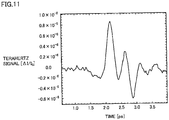
- the electro-optic polymer can have a larger figure of merit for the generation of a terahertz wave considering the electro-optic constant and a refractive index (n opt 6 r 2 /16n THz ; n opt : refractive index of material at wavelength of incident light, r: electro-optic constant, n THz : refractive index of material at wavelength of generated terahertz wave (" Organic Electro-Optics and Photonics" (L. R. Dalton, et.al., Cambridge University Press (2015 ))) than that of other material, whereby a highly efficient terahertz wave generating element (or detecting element) can be attained.
- the electric field during the poling processing using the poling electrodes is typically 100 V/ ⁇ m.
- poling processing is performed by subjecting an electro-optic polymer film to corona discharge.
- the electro-optic polymer film can be easily formed by a spin coating method or the like.
- the formed electro-optic polymer film can be processed into a waveguide by using a fine processing process such as photolithography or dry etching.
- NPL 1 F. A.Vallejo, L. M. Hayden, "Simplified model for optical rectification of broadband terahertz pulses in lossy waveguides including a new generalized expression for the coherence length,", Opt. Express, vol. 21, 24398-24412 (2013 )
- the present invention can provide a method for producing a laminate for non-linear optics that is not limited by the condition of poling processing.
- the "electro-optic polymer” (hereinafter, may be referred to as "EO polymer”) is a polymer that exhibits a second-order non-linear optical effect, and includes (1) a guest-host type electro-optic polymer obtained by mixing a matrix polymer with electro-optic molecules, (2) a side chain type electro-optic polymer containing electro-optic molecules covalently bonded to a side chain of a base polymer, (3) a main chain type electro-optic polymer containing electro-optic molecules covalently bonded in a main chain of a base polymer, (4) a cross-link type electro-optic polymer containing cross-linkage between matrix polymers or base polymers, or between a matrix polymer or a base polymer and electro-optic molecules, and the like, and (5) a molecular glass type electro-optic polymer.
- the guest-host type electro-optic polymer can also be grasped as a composition containing a matrix polymer and electro-opti
- Examples of the second-order non-linear optical effect include second-order harmonic generation, optical rectification, sum frequency generation, difference frequency generation, optical parametric oscillation/amplification, and an electro-optic effect (Pockels effect).
- Examples thereof include a (meth)acrylate-based polymer (for example, polymethyl methacrylate (PMMA)), polyamide, polyimide, polycarbonate (for example, poly[Bisphenol A carbonate-co-4,4'-(3,3,5-trimethylcyclohexylidene)diphenol carbonate] and the like), polydicyclopentanyl methacrylate (poly DCPMA), polyadamantyl methacrylate (poly AdMA), poly(DCPMA-co-MMA), poly(AdMA-co-MMA) and the like), a cycloolefin polymer, a cycloolefin copolymer, polystyrene, polyethylene, polymethylpentene, polypropylene, polyvinyl alcohol (PVA), polyethylene terephthalate, polysulfone, polyether sulfone, polyester, polyolefin, polyphenylene sulfide, polyurea, a silicon resin, an epoxy resin, and
- electro-optic molecules examples include compounds represented by the following structural formulae [A-1] to [A-7]. These can be used alone or in combination of two or more.
- the content ratio of the electro-optic molecules is not particularly limited, but it is usually about 1 to 70% by mass with respect to the total amount of the matrix polymer or the base polymer and the electro-optic molecules (corresponding to the total mass of the electro-optic polymer), preferably about 5 to 60% by mass, and more preferably about 10 to 50% by mass.
- the content ratio is the same even when the electro-optic polymer is in a side chain type or main chain type form.
- the content ratio of the electro-optic molecules is determined based on the electro-optic molecules derived from a side chain moiety.
- the content ratio of an electro-optic dye is determined based on an electro-optic molecular moiety in the main chain.
- the electro-optic polymer may be, for example, a side chain type electro-optic polymer having repeating units represented by the formulae (1) to (3).
- the side chain type electro-optic polymer may be a copolymer of a repeating unit (for example, a repeating unit represented by the formula (1) or the formula (3)) constituting a base polymer not containing an electro-optic molecular moiety as a side chain with a repeating unit (for example, a repeating unit represented by the formula (2)) constituting a base polymer containing an electro-optic molecular moiety as a side chain.
- the copolymer may be a random copolymer, a block copolymer, or a graft copolymer.
- the "supporting body” means a substrate carrying an electro-optic polymer layer.
- the supporting body may have a single layer structure or a plurality of layer structures, depending on the application of the produced laminate for non-linear optics to be produced.
- the supporting body can be appropriately set depending on the application of the laminate for non-linear optics to be produced.
- the supporting body examples include glass (for example, BK7 and the like), SiO 2 (for example, quartz glass), sol-gel glass (for example, MAPTMS and the like), a fluororesin (for example, PTFE, CYTOP (Asahi Glass Co., Ltd., registered trademark), Teflon (The Chemours Company, registered trademark) AF, and the like), polycarbonate (for example, poly[Bisphenol A carbonate-co-4,4'-(3,3,5-trimethylcyclohexylidene)diphenol carbonate] and the like), a (meth)acrylate polymer (for example, polymethyl methacrylate (PMMA), polydicyclopentanyl methacrylate (poly DCPMA), polyadamantyl methacrylate (poly AdMA), poly(DCPMA-co-MMA), poly(AdMA-co-MMA) and the like), a cycloolefin polymer (for example, ZEONEX (Zeon Corporation
- Examples of the supporting body include a semiconductor, an oxide, a nitride, an oxynitride, a ferroelectric compound, a metal, and a transparent conductive material.
- Examples of the semiconductor include IV group semiconductors such as diamond (C), silicon (Si), boron-doped silicon, phosphorus-doped silicon, silicon carbide (SiC), silicon germanium (SiGe) and germanium (Ge), III-V group semiconductors such as gallium arsenide (GaAs), indium phosphide (InP), gallium nitride (GaN) and gallium phosphide (GaP), and II-VI group semiconductors such as zinc selenide (ZnSe), cadmium sulfide (CdS), cadmium selenide (CdSe), telluride cadmium (CdTe), zinc sulfide (ZnS), zinc selenide (ZnSe), zinc telluride (Z
- oxide examples include silicon oxide, metal oxide [for example, titanium oxide (TiO 2 ), aluminum oxide (Al 2 O 3 ), hafnium oxide (HfO 2 ), lanthanum oxide (La 2 O 3 ), zirconium dioxide (ZrO 2 ), yttrium oxide (Y 2 O 3 ), tantalum pentoxide (Ta 2 O 5 ), zinc oxide (ZnO), gallium oxide (Ga 2 O 3 ), magnesium oxide (MgO), and the like], hafnium silicate (HfSiO 4 ), and silicon dioxide (SiO 2 ).
- metal oxide for example, titanium oxide (TiO 2 ), aluminum oxide (Al 2 O 3 ), hafnium oxide (HfO 2 ), lanthanum oxide (La 2 O 3 ), zirconium dioxide (ZrO 2 ), yttrium oxide (Y 2 O 3 ), tantalum pentoxide (Ta 2 O 5 ), zinc oxide (ZnO), gallium oxide (Ga 2 O
- nitride examples include silicon nitride, carbon nitride, and metal nitrides [for example, aluminum nitride (AlN), titanium nitride (TiN), and hafnium nitride (HfN) and the like].
- metal nitrides for example, aluminum nitride (AlN), titanium nitride (TiN), and hafnium nitride (HfN) and the like.
- oxynitride examples include silicon oxynitride, and metal oxynitrides [for example, aluminum oxynitride (AION) and hafnium oxynitride (HfON) and the like].
- ferroelectric compound examples include lithium niobate (LiNbO 3 ), lithium tantalate (LiTaO 3 ), and lanthanum-doped lead zirconate titanate (PLZT).
- metal examples include gold (Au), silver (Ag), copper (Cu), platinum (Pt), and aluminum (Al).
- transparent conductive material examples include ITO, IZO, FTO (fluorine-doped tin oxide), IGZO (InGaZnO), AZO (aluminum-doped zinc oxide), GZO (gallium-doped zinc oxide), and SnO 2 . These can be used alone or in combination of two or more. The materials are suitably used for a layer in contact with the electro-optic polymer layer when the supporting body has a plurality of layer structures.
- the "poling processing” means processing for orienting electro-optic molecules and fixing the orientation.
- the poling processing is not particularly limited. Examples thereof include a method for applying a voltage at a temperature near the glass transition temperature of an electro-optic polymer layer with the electro-optic polymer layer sandwiched between a lower electrode and an upper electrode, and a method for subjecting an electro-optic polymer layer to corona discharge.
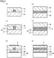
- an electro-optic polymer layer 10 may be subjected to poling processing as follows.
- a substrate 1, a lower electrode 2, electro-optic polymer layer 10, and an upper electrode 3 are laminated in this order, and a voltage is applied between lower electrode 2 and upper electrode 3 at a temperature near the glass transition temperature of electro-optic polymer layer 10.
- laminating means stacking an electro-optic polymer layer subjected to poling processing on a supporting body.
- the laminating step means eliminating a method for laminating an electro-optic polymer layer on a supporting body, and thereafter applying a voltage to the electro-optic polymer layer (poling processing), which has been conventionally performed.
- the laminating step is not particularly limited, and examples thereof include a method for transferring an electro-optic polymer layer subjected to poling processing on a lower electrode onto a supporting body.
- the laminating method is preferably performed by bonding the surface of the electro-optic polymer layer and the surface of the supporting body through a covalent bond, an electrostatic interaction, or a van der Waals interaction, or the like.
- FIG. 1(b) After the poling processing is completed ( Fig. 1(b) ), an upper electrode 3 is first removed by wet etching and the like ( Fig. 1(c) , Fig. 2(a) ). Thereafter, the surface of an electro-optic polymer layer 11 subjected to poling processing is subjected to oxygen plasma processing to activate the surface ( Fig. 2(b) ).
- -COR in Fig. 2(b) represents an organic group containing a carbonyl group.
- the surface of a supporting body 20 is subjected to oxygen plasma processing, and further processed by a silane coupling agent having an amino group, and the like to activate the surface ( Figs. 2(c) and 2(d) ).
- electro-optic polymer layer 11 subjected to poling processing is transferred to supporting body 20 so that the activated surfaces face each other, and a substrate 1 and a lower electrode 2 are removed to obtain a laminate for non-linear optics 50 ( Fig. 1(d) , Fig. 2(e) ).
- the silane coupling agent having an amino group is used as a reagent for bringing electro-optic polymer layer 11 and supporting body 20 into close contact, but in addition to this, a silane coupling agent having a vinyl group, an epoxy group, a styryl group, a methacryl group, an acryl group, an isocyanate group, an isocyanurate group, a ureido group, or a mercapto group, and the like may be used.
- the surface of electro-optic polymer layer 11 and the surface of supporting body 20 may be subjected to oxygen plasma processing to transfer electro-optic polymer layer 11 subjected to poling processing onto supporting body 20 so that the activated surfaces face each other.
- the surface of supporting body 20 may be subjected to oxygen plasma processing, and further processed by a silane coupling agent having an amino group to activate the surface, and electro-optic polymer layer 11 may be transferred onto supporting body 20 so that the activated surface of supporting body 20 and the surface of unprocessed electro-optic polymer layer 11 not subjected to oxygen plasma processing and silane coupling processing face each other.
- electro-optic polymer layer 10 is simply supported on lower electrode 2 by a spin coating method, substrate 1 and lower electrode 2 can be removed by merely peeling off substrate 1 and lower electrode 2 from transferred electro-optic polymer layer 11 without being subjected to special processing.
- Examples of another embodiment of the method for producing a laminate for non-linear optics according to the present embodiment include the following method. First, a roll of a long electro-optic polymer film (electro-optic polymer layer) and a roll of a long film type supporting body are prepared. The films are transported while the films are continuously unwound using an unwinding device. Each film is transported so that the longitudinal direction thereof is a transport direction.
- the electro-optic polymer film that has been transported is subjected to corona discharge and the like to subject the electro-optic polymer film to poling processing (step of poling processing).
- the electro-optic polymer film subjected to poling processing and the film type supporting body that are continuously transported are overlapped so that the longitudinal directions thereof (transport directions) are parallel to each other.
- a laminate of the overlapped films (laminate for non-linear optics) is passed between a pair of pasting rolls, to apply a pressure to the laminate, thereby pasting the films (step of laminating the electro-optic polymer layer on the supporting body).
- the producing method according to the present embodiment may further include other steps such as a step of processing the electro-optic polymer layer subjected to poling processing after the above-described steps.
- Examples of the other processing include:
- the laminate for non-linear optics contains the electro-optic molecules oriented in a predetermined direction
- the laminate for non-linear optics has a second-order non-linear optical effect.
- the second-order non-linear optical effect increases in proportion to the square of the intensity of an electromagnetic wave. Therefore, a frequency conversion efficiency is improved by using an electro-optic polymer waveguide having a small cross-sectional area and a large optical confinement effect, and the like.
- the second-order non-linear optical effect increases as an interaction distance between the electromagnetic wave and the electro-optic molecules increases. Therefore, frequency conversion can be efficiently performed by using an electro-optic polymer waveguide having a long waveguide length.
- the power of a laser beam that can be introduced can be increased as the thickness of the layer (cross-sectional area) increases, which makes it possible to improve the power of a generated terahertz wave.
- one or more other layers may be further laminated on the electro-optic polymer layer laminated on the supporting body.
- the other layer may be composed of the same component as that of the supporting body or the electro-optic polymer layer, or may be composed of a different component.
- the thickness of the electro-optic polymer layer can be appropriately set depending on the application of the laminate for non-linear optics, but it may be greater than or equal to 0.01 ⁇ m and less than or equal to 50 cm, greater than or equal to 0.05 ⁇ m and less than or equal to 10 cm, or greater than or equal to 0.5 ⁇ m and less than or equal to 1 cm.
- the "thickness of the electro-optic polymer layer” means the shortest distance between two surfaces of the electro-optic polymer layer perpendicular to the laminating direction in the laminate for non-linear optics.
- the "thickness of the electro-optic polymer layer” can also be grasped as the shortest distance between two principal surfaces facing each other in the electro-optic polymer layer.
- the thickness is obtained as an average value of values measured at optional 3 to 10 positions by a stylus profile measuring method, an electron microscope method, an optical microscope method, an ellipsometry method, or a micrometer or the like.
- the thickness of the supporting body can be appropriately set depending on the application of the laminate for non-linear optics, but it may be greater than or equal to 0.01 ⁇ m and less than or equal to 1000 cm, greater than or equal to 10 ⁇ m and less than or equal to 1000 cm, greater than or equal to 20 ⁇ m and less than or equal to 100 cm, greater than or equal to 30 ⁇ m and less than or equal to 10 cm, or greater than or equal to 40 ⁇ m and less than or equal to 1 cm.
- the "thickness of the supporting body” means the shortest distance between the two surfaces of the supporting body perpendicular to the laminating direction in the laminate for non-linear optics.
- the thickness of the supporting body can also be grasped as the shortest distance between two principal surfaces facing each other in the supporting body.
- the thickness is obtained as an average value of values measured at optional 3 to 10 positions by a stylus profile measuring method, an electron microscope method, an optical microscope method, an ellipsometry method, or a micrometer or the like.
- the adhesive strength between the supporting body and the electro-optic polymer layer is preferably greater than or equal to 0.01 N/mm 2 and less than or equal to 20 N/mm 2 , more preferably greater than or equal to 0.05 N/mm 2 and less than or equal to 10 N/mm 2 , and greater than or equal to 0.1 N/mm 2 and less than or equal to 5 N/mm 2 .
- the adhesive strength can be measured by, for example, a pull-off method.
- the laminate for non-linear optics according to the present embodiment is suitably used for producing a non-linear optical element.
- the non-linear optical element include a waveguide element for terahertz wave, a non-linear optical element for high-power laser, and a light modulation element.
- each non-linear optical element will be described.
- the waveguide element for terahertz wave includes the laminate for non-linear optics (including the supporting body and the electro-optic polymer layer).
- the supporting body contains a cycloolefin polymer or a cycloolefin copolymer.
- the cycloolefin polymer and the cycloolefin copolymer have a small terahertz wave absorption loss. Therefore, the waveguide element for terahertz wave according to the present embodiment can efficiently generate or detect a terahertz wave.
- a lower poling electrode is first formed on a substrate, and a clad layer, a core layer containing an electro-optic polymer, and a clad layer are formed in this order on the lower poling electrode. Furthermore, an upper poling electrode is formed on the clad layer. Thereafter, the electro-optic polymer is subjected to poling processing by applying a voltage between the two poling electrodes (PTLs 1 to 5).
- a material used for a clad layer around a core layer containing an electro-optic polymer had to have a lower electrical resistivity than that of the electro-optic polymer from the viewpoint of suppressing voltage drop in the clad layer in poling processing.
- the electrical resistivity of the material used for the clad layer is typically 10 8 ⁇ m.
- the clad layer that is present during poling processing and has a small electrical resistivity remains as it is even in the produced waveguide element.
- terahertz wave low absorption loss material a material having a small terahertz wave absorption loss
- the electrical resistivity of the clad layer is larger than the electrical resistivity of the core layer containing the electro-optic polymer, large voltage drop occurs in a portion of the clad layer even when a predetermined voltage is applied, and a voltage applied to the core layer containing the electro-optic polymer is decreased, so that efficient poling processing cannot be performed.
- the use of the terahertz wave low absorption loss material for the clad layer has been suggested by simulations in the design of the waveguide element for terahertz wave ( F. A. Vallejo, L. M.
- Hayden "Simplified model for optical rectification of broadband terahertz pulses in lossy waveguides including a new generalized expression for the coherence length,", Opt. Express, vol. 21, 24398-24412 (2013 ) (NPL 1)), but such a specific method for producing a waveguide element has not been revealed so far.
- the waveguide element for terahertz wave according to the present embodiment is produced by subjecting an electro-optic polymer layer as a core layer to poling processing according to the method for producing a laminate for non-linear optics according to the present embodiment, and thereafter laminating the core layer subjected to poling processing on a clad layer (supporting body) containing a terahertz wave low absorption loss material. This is possible to produce a predetermined waveguide element for terahertz wave without being limited by the condition of the poling processing.
- the cycloolefin polymer is a polymer of a cycloolefin, and examples thereof include polynorbornene.
- the cycloolefin includes a polymerizable cycloolefin having an ethylenic double bond, and includes a bicyclic olefin, a monocyclic olefin, or a tricyclic or higher polycyclic olefin.
- Typical examples of the bicyclic olefin include norbornene (2-norbornene) that may have a substituent.
- Examples of the monocyclic olefin include cyclic C 4-12 cycloolefins such as cyclobutene, cyclopentene, cycloheptene, and cyclooctene.
- Examples of the polycyclic olefin include dicyclopentadiene that may have a substituent.
- the cycloolefin polymer may be, for example, a polymer having a repeating unit represented by the formula (4) (wherein n represents a positive integer). These can be used alone or in combination of two or more.
- Examples of the cycloolefin copolymer include a copolymer of a cycloolefin and a chain olefin, a copolymer of a cycloolefin polymer and an olefin polymer, and a copolymer of a first cycloolefin polymer and a second cycloolefin polymer.
- Examples of the chain olefin include chain C 2-10 olefins such as ethylene, propylene, 1-butene, isobutene, 1-pentene, 3-methyl-1-pentene, 1-hexene, and 1-octene.
- the copolymer may be a random copolymer, a block copolymer, or a graft copolymer.
- the cycloolefin copolymer may be, for example, a copolymer having a repeating unit represented by the formula (5) (wherein x and y each represent a positive integer). These can be used alone or in combination of two or more.
- a commercially available cycloolefin polymer and cycloolefin copolymer may be used.
- Examples of the commercially available cycloolefin polymer include ZEONEX (registered trademark), ZEONOR (registered trademark), and ARTON (registered trademark).
- Examples of the commercially available cycloolefin copolymer include TOPAS (registered trademark) and APEL (registered trademark).
- Fig. 1 is a schematic view showing an example of a method for producing a laminate for non-linear optics and a waveguide including the laminate.
- a plurality of arrows drawn in an electro-optic polymer layer 11 subjected to poling processing indicate that electro-optic molecules in electro-optic polymer layer 11 are oriented.
- an example of a method for producing a waveguide element for terahertz wave will be described with reference to Fig. 1 .
- a lower electrode 2 is formed on a substrate 1, and an electro-optic polymer layer 10 is formed thereon by a spin coating method or the like.
- an upper electrode 3 is formed on electro-optic polymer layer 10.
- electro-optic polymer layer 10 is subjected to poling processing by applying a predetermined voltage between lower electrode 2 and upper electrode 3 at a temperature near the glass transition temperature of the electro-optic polymer layer ( Figs. 1(a) and 1(b) ).
- upper electrode 3 is removed by wet etching or the like ( Fig. 1(c) , Fig. 2(a) ), and oxygen plasma processing using a reactive ion etching apparatus and the like is performed ( Fig. 2(b) ).
- a terahertz wave low absorption loss material supporting body 20 subjected to oxygen plasma processing using the reactive ion etching apparatus and the like is processed by a silane coupling agent having an amino group, and the like ( Figs. 2(c) and 2(d) ).
- electro-optic polymer layer 11 is transferred by subjecting both the substrates to pressure bonding while applying heat, and substrate 1 and lower electrode 2 are removed ( Figs. 1(d) , 2(e) ).
- transferred electro-optic polymer layer 11 is processed into a waveguide structure by dry etching and the like ( Fig. 1(e) ).
- a solution containing a terahertz wave low absorption loss material is applied onto a waveguide structure 12, thereby forming an upper clad layer 25 containing the terahertz wave low absorption loss material ( Fig. 1(f) ).
- the waveguide element for terahertz wave including upper and lower clad layers containing the terahertz wave low absorption loss material is produced.
- Fig. 3 is a schematic view showing an example of a waveguide element for terahertz wave including a laminate for non-linear optics produced by the producing method of the present embodiment.
- the schematic view shows the cross section of a waveguide.
- clad layers 20 and 25 containing a terahertz wave low absorption loss material are disposed above and below waveguides 13 and 14 containing the electro-optic polymer subjected to poling processing so as to be in contact with waveguides 13 and 14.
- Figs. 3 In the structures shown in Figs.
- layers 6 and 22 containing a material having a larger refractive index than that of the electro-optic polymer layer constituting guides 13 and 14 are disposed so as to be in contact with waveguides 13 and 14.
- clad layers 21 and 25 containing a terahertz wave low absorption loss material are disposed above and below high refractive index material layers 6 and 22.
- the waveguide elements having the structures shown in Figs. 3(c) and 3(d) are produced using a supporting body 23 including a clad layer 21 and a high refractive index material layer 22. In the structures shown in Figs.
- clad layers 20 and 25 containing a terahertz wave low absorption loss material are disposed above and below waveguide 13 so as to be in contact with waveguide 13. Furthermore, metal layers 5 and 5 are disposed above and below clad layers 20 and 25.
- the waveguide elements having the structures shown in Fig. 3(e) and 3(f) are produced using a supporting body 26 including a substrate 4, a metal layer 5, and a clad layer 20.
- clad layers 20, 21, and 25 including a terahertz wave low absorption loss material are disposed around waveguides 12, 13, and 14 including an electro-optic polymer layer.
- the terahertz waves generated from waveguides 12, 13, and 14 including the electro-optic polymer layer are less likely to be absorbed and lost by clad layers 20, 21, and 25, whereby the terahertz waves can be efficiently generated.
- the terahertz wave that is detected and introduced from the outside is less likely to be absorbed and lost by clad layers 20, 21, and 25, whereby the terahertz wave can be efficiently detected.
- the shape of the waveguide is not particularly limited, and examples thereof include a slab type, a channel type, a ridge type, and a rib type.
- dry etching, reactive ion etching, a photolithography method, an imprinting method, and a photobleaching method and the like can be used.
- a non-linear optical element for high-power laser according to the present embodiment includes the laminate for non-linear optics according to the present embodiment (including a supporting body and an electro-optic polymer layer), in which the electro-optic polymer layer has a thickness of greater than or equal to 5 ⁇ m and less than or equal to 50 cm.
- the thickness of the electro-optic polymer layer is greater than or equal to 5 ⁇ m and less than or equal to 50 cm, whereby the output (power) of the laser beam to be introduced can be increased, which provides improved power of the generated terahertz wave.
- the conventional technique made it necessary to apply a high voltage in order to subject an electro-optic polymer film having a large film thickness to poling processing when a non-linear optical element including an electro-optic polymer film is produced.
- a general-purpose high-voltage power supply which disadvantageously causes a limited thickness of the electro-optic polymer film that can be subjected to poling processing.
- a large current flows due to a charge injection barrier at the interface between an electrode for poling processing and the electro-optic polymer film, which causes breakdown.
- the electro-optic polymer film is broken by the breakdown, which disadvantageously causes a limited thickness of the electro-optic polymer film that can be subjected to poling processing.
- the non-linear optical element for high-power laser according to the present embodiment can be produced by a method for producing a laminate for non-linear optics according to the present embodiment. Specifically, first, a laminate for non-linear optics is produced by a method including:
- a second electro-optic polymer layer having the same composition as the composition of the first electro-optic polymer layer is subjected to poling processing, and the second electro-optic polymer layer subjected to poling processing is then laminated on the first electro-optic polymer layer in the laminate for non-linear optics.
- a third electro-optic polymer layer having the same composition as the composition of the first electro-optic polymer layer may be subjected to poling processing, and the third electro-optic polymer layer subjected to poling processing may be then laminated on the second electro-optic polymer layer in the laminate for non-linear optics.
- the "high power laser” means a laser having a peak output of greater than or equal to 10 ⁇ 10 -3 W and less than or equal to 1 ⁇ 10 14 W.
- the peak output is preferably greater than or equal to 20 ⁇ 10 -3 W and less than or equal to 1 ⁇ 10 12 W, and more preferably greater than or equal to 50 ⁇ 10 -3 W and less than or equal to 5 ⁇ 10 11 W.
- the electro-optic polymer layer has a thickness of greater than or equal to 5 ⁇ m and less than or equal to 50 cm, preferably greater than or equal to 10 ⁇ m and less than or equal to 10 cm, and more preferably greater than or equal to 20 ⁇ m and less than or equal to 1 cm.
- Fig. 4 is a schematic view showing an example of a method for producing a laminate for non-linear optics for high-power lasers. By repeating the laminating process a plurality of times ( Figs. 4(d), 4(e), and 4(f) ), a laminate for non-linear optics including an electro-optic polymer layer having a large thickness is produced.
- the laminate for non-linear optics shown in Fig. 4 includes an electro-optic polymer layer having an optional large thickness
- the laminate for non-linear optics is suitably used for producing a non-linear optical element for high-power laser.
- the thickness of the electro-optic polymer layer increases, the power of a laser beam that can be introduced into the electro-optic polymer layer can be increased. Therefore, the power of the terahertz wave generated in the non-linear optical element is improved.
- a light modulation element includes the laminate for non-linear optics according to the present embodiment (including a supporting body and an electro-optic polymer layer), in which the supporting body contains at least one selected from the group consisting of glass, SiO 2 , sol-gel glass, a fluororesin, polycarbonate, a (meth)acrylate polymer, a cycloolefin polymer, a cycloolefin copolymer, polystyrene, polyethylene, polymethylpentene, polypropylene, polyimide, polyvinyl alcohol, polyethylene terephthalate, an ultraviolet curable resin, silicon, gallium arsenide, indium phosphide, titanium oxide, zinc oxide, aluminum oxide, silicon nitride, aluminum nitride, ITO, IZO, and IGZO.
- the supporting body contains at least one selected from the group consisting of glass, SiO 2 , sol-gel glass, a fluororesin, polycarbonate, a (meth
- the light modulation element according to the present embodiment has the above configuration, whereby the light modulation element can be used at a lower operating voltage and power consumption than those of the conventional light modulation element.
- the light modulation element according to the present embodiment is produced by subjecting an electro-optic polymer layer as a core layer to poling processing according to the method for producing a laminate for non-linear optics according to the present embodiment, and thereafter laminating the core layer subjected to poling processing on a supporting body (clad layer) containing an optional material. Therefore, it becomes possible to produce a predetermined light modulation element without being limited by the condition of the poling processing.
- Fig. 5 is a schematic view showing an example of a light modulation element including a laminate for non-linear optics produced by the producing method according to the present embodiment.
- clad layers 20 and 25 including a low refractive index material are disposed around a waveguide 13 including an electro-optic polymer layer. It has been known that, as the refractive indexes of clad layers 20 and 25 with respect to the refractive index of waveguide 13 are smaller, a mode size in the waveguide is smaller. As the mode size is smaller, the interaction between the mode and light modulation electrodes 7 and 7 disposed above and below is smaller, which causes a decreased loss of light. Therefore, the distance between light modulation electrodes 7 and 7 can be reduced, which can provide a decreased operating voltage. That is, the light modulation element shown in Fig. 5 has an effect of reducing the operating voltage and power consumption of a light modulator.
- the material used for the supporting body is not particularly limited as long as the material forms the waveguide together with the electro-optic polymer layer.
- the material used for the supporting body contains, for example, at least one selected from the group consisting of glass (for example, BK7 and the like), SiO 2 (for example, quartz glass), sol-gel glass (for example, MAPTMS and the like), a fluororesin (for example, PTFE, CYTOP, Teflon AF and the like), polycarbonate (for example, poly[Bisphenol A carbonate-co-4,4'-(3,3,5-trimethylcyclo-hexylidene)diphenol carbonate] and the like), a (meth)acrylate polymer (for example, polymethyl methacrylate (PMMA), polycyclopentanyl methacrylate (poly DCPMA), polyadamantyl methacrylate (poly AdMA), poly (DCPMA-co-MMA), poly (AdMA-co-MMA), and the like), a
- the electrode is not particularly limited, and examples thereof include indium tin oxide (ITO), gold, silver, chromium, aluminum, titanium, indium zinc oxide (IZO), and aluminum-doped zinc oxide. These can be used alone or in combination of two or more.
- ITO indium tin oxide
- IZO indium zinc oxide
- aluminum-doped zinc oxide aluminum-doped zinc oxide.
- a free-standing electro-optic polymer laminate according to the present embodiment includes the laminate for non-linear optics according to the present embodiment (including a supporting body and an electro-optic polymer layer), in which the supporting body is an electro-optic polymer having the same composition as or a different composition from the composition of the electro-optic polymer layer.
- the free-standing electro-optic polymer laminate according to the present embodiment can be used for applications such as a terahertz wave generation device, a terahertz wave detection device, and a light modulation element.
- the "free-standing electro-optic polymer laminate” means a laminate including the plurality of electro-optic polymer layers, in which the supporting body is an electro-optic polymer.
- the supporting body in the free-standing electro-optic polymer laminate can also be grasped as the electro-optic polymer layer subjected to poling processing.
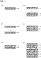
- Fig. 12 is a schematic view showing an example of a method for producing a free-standing electro-optic polymer laminate. Specifically, by a method including a step of subjecting a first electro-optic polymer layer to poling processing ( Fig. 12(a) ), a step of subjecting a second electro-optic polymer layer having the same composition as or a different composition from the composition of the first electro-optic polymer layer to poling processing, and a step of laminating the second electro-optic polymer layer subjected to poling processing on the first electro-optic polymer layer subjected to poling processing ( Figs. 12(b) and 12(c) ), the free-standing electro-optic polymer laminate is produced.
- a third electro-optic polymer layer having the same composition as or a different composition from the composition of the first electro-optic polymer layer may be subjected to poling processing, and the third electro-optic polymer layer subjected to poling processing may be then laminated on the second electro-optic polymer layer in the free-standing electro-optic polymer laminate ( Figs. 12(d) and 12(e) ). Furthermore, another new free-standing electro-optic polymer laminate may be laminated on the free-standing electro-optic polymer laminate.
- a free-standing electro-optic polymer laminate having a predetermined thickness can be produced without being limited by the condition of the poling processing (( Fig. 12(f) ).
- the thickness of the free-standing electro-optic polymer laminate can be appropriately set according to the application of the free-standing electro-optic polymer laminate.
- the thickness of the free-standing electro-optic polymer laminate may be greater than or equal to 0.02 ⁇ m and less than or equal to 50 cm, greater than or equal to 0.1 ⁇ m and less than or equal to 40 cm, greater than or equal to 1 ⁇ m and less than or equal to 10 cm, or greater than or equal to 10 ⁇ m and less than or equal to 1 cm.
- a side chain type electro-optic polymer (random copolymer) layer (hereinafter, may be referred to as "electro-optic polymer layer") containing repeating units represented by the following chemical formulae (1) to (3) (wherein p, q and r each represent a positive integer) by a spin coating method was formed on an indium tin oxide electrode (ITO electrode).
- ITO electrode indium tin oxide electrode
- the thickness of the electro-optic polymer layer was 2.4 to 2.6 ⁇ m as measured by a stylus profile measuring method.
- the thickness was determined as an average value of values measured at three locations on the main surface of the electro-optic polymer layer.
- An indium zinc oxide electrode (IZO electrode) was formed on the electro-optic polymer layer by a sputtering method to obtain a sample before poling processing.
- the electro-optic polymer layer was then subjected to poling processing by applying a voltage of 110 to 115 V/ ⁇ m between the ITO electrode and the IZO electrode while heating the sample to a temperature of 150°C that was close to the glass transition point (160°C) of the electro-optic polymer, and cooled to room temperature while maintaining the voltage.
- the electro-optic constant (r 33 ) of the electro-optic polymer layer measured by a transmission ellipsometry method ( T. Yamada, A.
- a cycloolefin copolymer (TOPAS (registered trademark) 5013) supporting body subjected to oxygen plasma processing using the reactive ion etching apparatus was processed by a silane coupling agent having an amino group (KBP-90, manufactured by Shin-Etsu Chemical Co., Ltd.) (hereinafter, the obtained sample may be referred to as "sample B").
- a cycloolefin polymer (ZEONEX (registered trademark) 480R) supporting body subjected to oxygen plasma processing using the reactive ion etching apparatus was processed by the silane coupling agent having an amino group (hereinafter, the obtained sample may be referred to as "sample C").
- the electro-optic polymer layer was transferred and laminated onto the cycloolefin copolymer or cycloolefin polymer supporting body.
- the adhesive strength between the electro-optic polymer layer and the supporting body in the laminate for non-linear optics obtained by subjecting sample A and sample B to pressure bonding was 0.75 N/mm 2 as measured by a pull-off method.
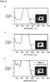
- Fig. 6 showed absorption spectra in the terahertz wave band of the cycloolefin copolymer and the cycloolefin polymer used as the supporting body ( Figs. 6(a) and 6(b) ).
- the absorption coefficients of the cycloolefin copolymer and cycloolefin polymer at 0.1 to 10 THz were less than or equal to 5 cm -1 .
- the absorption spectrum in the terahertz region of polymethyl methacrylate (PMMA) that was a general polymer as a transparent resin, as with the cycloolefin copolymer or the cycloolefin polymer, was shown ( Fig. 6(c) ).
- the cycloolefin copolymer and the cycloolefin polymer used as the supporting body have smaller absorption in the terahertz wave band than that of a general polymer, and are suitable as a clad layer of a waveguide element for terahertz wave.
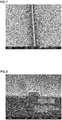
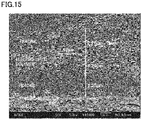
- a mask was then formed on the electro-optic polymer layer by photolithography, and the electro-optic polymer layer was processed into a waveguide structure by a dry etching method using a reactive ion etching apparatus ( Figs. 7 and 8).
- Fig. 7 is a channel type electro-optic polymer waveguide structure (top image) on a cycloolefin copolymer supporting body.
- Fig. 8 is a ridge type electro-optic polymer waveguide structure (cross-sectional image) on a cycloolefin polymer supporting body.
- sample D A silicon supporting body including a thermal oxide film subjected to oxygen plasma processing using a reactive ion etching apparatus was processed by a silane coupling agent having an amino group (hereinafter, the obtained sample may be referred to as "sample D").
- sample A and sample D By subjecting sample A and sample D to pressure bonding at 100°C so that the processed surfaces faced each other, the electro-optic polymer layer was transferred and laminated onto the silicon supporting body.
- the surface of the electro-optic polymer layer transferred onto the silicon supporting body was subjected to oxygen plasma processing using the reactive ion etching apparatus, and processed by a silane coupling agent having an amino group (hereinafter, the obtained sample may be referred to as "sample E").
- the electro-optic polymer layer was further transferred and laminated onto the electro-optic polymer layer on the silicon supporting body.
- a laminate for non-linear optics was prepared, in which three electro-optic polymer layers were laminated.
- the thickness of the laminated electro-optic polymer layer was 7.4 ⁇ m as measured by a stylus profile measuring method ( Fig. 9 ).
- a cylinder having a diameter of 7 mm and the electro-optic polymer layer laminated on the supporting body were bonded to each other using a two-component mixed epoxy adhesive.
- the adhesive was cured, and the cylinder was then pulled up at a speed of 1 mm/min using a precision universal testing machine (Autograph, manufactured by Shimadzu Corporation) to measure a force (adhesive strength) at which the electro-optic polymer layer and the supporting body were peeled off from each other.
- the adhesive strength between the electro-optic polymer layer and the supporting body is large, which provides effects such as an effect of preventing the electro-optic polymer layer from being peeled from the supporting body when a non-linear optical element is diced.
- Sample A and sample C were prepared in the same manner as in Example 1.
- an electro-optic polymer layer was transferred and laminated onto a cycloolefin polymer supporting body.
- the surface of the electro-optic polymer layer of the obtained sample was subjected to oxygen plasma processing using a reactive ion etching apparatus in the same manner as in the preparation of sample A (hereinafter, may be referred to as "sample F").
- sample F reactive ion etching apparatus
- a laminate corresponding to Fig. 3(b) was prepared.
- a scanning electron microscope image of the cross section of the laminate is shown in Fig. 10 .
- the thickness of the electro-optic polymer layer in the prepared laminate was 4.5 ⁇ m, and the electro-optic constant (r 33 ) at a wavelength of 1550 nm was 45 pm/V.
- a terahertz wave was generated by irradiating a laminate having a device length of 1.0 mm with a 20 mW femtosecond pulse laser (center wavelength: 1.56 ⁇ m, pulse width: 100 fs or less, repetition frequency: 50 MHz).
- the terahertz wave was detected by an electro-optic sampling method using probe light having a wavelength of 780 nm and zinc telluride having a thickness of 1 mm.
- the probe light was superimposed on the terahertz wave in a zinc telluride crystal, and the polarization state of the probe light was changed by a Pockels effect induced by a terahertz electric field.
- the probe light having a changed polarization state was separated into two types of polarization components (longitudinally polarized light and laterally polarized light) after passing through a ⁇ /4 plate and a polarizing prism.
- the separated polarization components were detected by two detectors of a balance detector.
- the total power of the probe light input to the two detectors in the balance photodetector was 60 ⁇ W.
- Fig. 11 shows a time waveform of a terahertz wave obtained by an electro-optic sampling method.
- the ratio ( ⁇ I/I 0 ) of the change amount of probe light intensity to the total light intensity of the probe light is proportional to the terahertz electric field. From the results of Fig. 11 , the generation of the terahertz wave from the laminate was confirmed.
- An electro-optic polymer laminate (free-standing electro-optic polymer laminate) was prepared, in which a supporting body was an electro-optic polymer layer subjected to poling processing.
- Fig. 12 shows an example of a process for preparing an electro-optic polymer laminate when a supporting body is an electro-optic polymer layer subjected to poling processing.
- an electro-optic polymer layer was formed on an ITO electrode.
- An IZO electrode was formed on the electro-optic polymer layer, and subjected to poling processing, followed by removing the IZO electrode.
- a first electro-optic polymer layer (thickness: 2.8 ⁇ m) subjected to poling processing and a second electro-optic polymer layer (thickness: 3.1 ⁇ m) subjected to poling processing were prepared.
- the surfaces of the first electro-optic polymer layer and the second electro-optic polymer layer were subjected to oxygen plasma processing by the same method as that in Example 1.
- the first electro-optic polymer layer and the second electro-optic polymer layer were laminated.
- the free-standing electro-optic polymer laminate hereinafter, may be referred to as "laminate" was prepared.
- the absorbance spectrum of the laminate is almost equal to the sum of the absorbance spectra of the first electro-optic polymer layer subjected to poling processing and the second electro-optic polymer layer subjected to poling processing.
- Fig. 14 shows thin film interference spectra (interference spectra due to thin film interference) of (a) a first electro-optic polymer layer subjected to poling processing (2.8 ⁇ m) (supporting body), (b) a second electro-optic polymer layer subjected to poling processing prior to lamination (3.1 ⁇ m), and (c) the laminate (5.9 ⁇ m).
- the thickness d of the thin film can be calculated from the wavelengths of the peak and valley of the interference spectrum, the wavelengths of the peaks or the wavelengths of the valleys, and the refractive index n of the thin film.
- the refractive index of the electro-optic polymer layer used is 1.6 at a wavelength of 1550 nm.
- the first electro-optic polymer layer, the second electro-optic polymer layer, and the layer thickness (film thickness) of the laminate were calculated.
- the refractive index was assumed to be 1.6 at the wavelengths of the adjacent peak and valley.
- the layer thickness of the laminate coincides with the sum of the layer thicknesses of the first electro-optic polymer layer subjected to poling processing and second electro-optic polymer layer subjected to poling processing.
- the homogeneous and independent laminate (free-standing electro-optic polymer laminate) having a predetermined thickness from the optical viewpoint was confirmed to be formed.
- sample G A sample having a surface having an electro-optic polymer layer formed thereon was prepared in the same manner as in sample A of Example 1 (hereinafter, the obtained sample may be referred to as "sample G").
- the glass transition temperature of the electro-optic polymer used for the preparation of sample G was 178°C; the temperature of poling processing was 165°C; and the electric field during poling was 120 V/ ⁇ m.
- the electro-optic constant (r 33 ) of the measured electro-optic polymer layer was 60 pm/V at a wavelength of 1308 nm and 42 pm/V at a wavelength of 1550 nm.
- An IZO lower electrode of an optical modulator was formed on a silicon substrate with a thermal oxide film having a thickness of 2 ⁇ m by a sputtering method.
- an ultraviolet curable resin (FE4048, manufactured by NTT-AT) as a supporting body was applied by a spin coating method, irradiated with 365 nm LED light, and then heated at 100°C for 2 hours.
- the surface of the supporting body of the ultraviolet curable resin was subjected to oxygen plasma processing using a reactive ion etching apparatus and processed by a silane coupling agent having an amino group (hereinafter, the obtained sample may be referred to as "sample H").
- Sample G and sample H were subjected to pressure bonding at 100°C so that the processed surfaces faced each other, thereby transferring and laminating the electro-optic polymer layer onto the supporting body of the ultraviolet curable resin.
- a mask was formed on the electro-optic polymer layer by photolithography, and the electro-optic polymer layer was processed into a rectangular structure (1.62 ⁇ m ⁇ 1.29 ⁇ m) by a dry etching method using a reactive ion etching apparatus.
- the optical waveguide forms a Mach-Zehnder (MZ) type optical modulator structure.
- an ultraviolet curable resin FE4048, manufactured by NTT-AT
- Fig. 15 is a cross-sectional image of a light incident part of the prepared light modulation element.
- a channel type electro-optic polymer waveguide structure can be confirmed on an ultraviolet curable resin supporting body.
- Fig. 16 shows the time waveform of light modulation.
- a channel 1 represents an applied voltage
- a channel 3 represents the output light intensity of an MZ light modulator.
- the light output waveform of a typical MZ light modulator with respect to the voltage change of a triangular waveform was shown, and a ⁇ phase modulation voltage (voltage between the minimum value and the maximum value) was 8.4 V.
Landscapes
- Physics & Mathematics (AREA)
- Nonlinear Science (AREA)
- Optics & Photonics (AREA)
- Electromagnetism (AREA)
- General Physics & Mathematics (AREA)
- Engineering & Computer Science (AREA)
- Plasma & Fusion (AREA)
- Optical Modulation, Optical Deflection, Nonlinear Optics, Optical Demodulation, Optical Logic Elements (AREA)
- Optical Integrated Circuits (AREA)
- Lasers (AREA)
Applications Claiming Priority (2)
| Application Number | Priority Date | Filing Date | Title |
|---|---|---|---|
| JP2017161292 | 2017-08-24 | ||
| PCT/JP2018/031089 WO2019039530A1 (ja) | 2017-08-24 | 2018-08-23 | 電気光学ポリマー層を含む非線形光学用積層体及びその製造方法 |
Publications (2)
| Publication Number | Publication Date |
|---|---|
| EP3674792A1 true EP3674792A1 (de) | 2020-07-01 |
| EP3674792A4 EP3674792A4 (de) | 2021-04-14 |
Family
ID=65439080
Family Applications (1)
| Application Number | Title | Priority Date | Filing Date |
|---|---|---|---|
| EP18848353.1A Pending EP3674792A4 (de) | 2017-08-24 | 2018-08-23 | Laminat für eine nichtlineare optik mit einer elektrooptischen polymerschicht und verfahren zu dessen herstellung |
Country Status (4)
| Country | Link |
|---|---|
| US (1) | US11194225B2 (de) |
| EP (1) | EP3674792A4 (de) |
| JP (2) | JP7244924B2 (de) |
| WO (1) | WO2019039530A1 (de) |
Families Citing this family (10)
| Publication number | Priority date | Publication date | Assignee | Title |
|---|---|---|---|---|
| KR102568796B1 (ko) * | 2018-06-15 | 2023-08-21 | 삼성전자주식회사 | 광변조 소자 및 이를 포함하는 장치 |
| KR102574503B1 (ko) * | 2020-08-21 | 2023-09-06 | 한국과학기술원 | 시공간적으로 유전율이 변조되는 광학적 물질을 포함하는 파라메트릭 소자 |
| US12300870B2 (en) | 2020-08-21 | 2025-05-13 | Korea Advanced Institute Of Science And Technology | Parametric device comprising optical materials spatiotemporally varying permittivity |
| TWI803954B (zh) * | 2021-08-27 | 2023-06-01 | 國立清華大學 | 太赫茲光調制器及太赫茲空間光調制器 |
| JP7842399B2 (ja) * | 2022-02-07 | 2026-04-08 | 日本放送協会 | 光偏向素子およびその製造方法 |
| JP7840558B2 (ja) * | 2022-02-25 | 2026-04-06 | 国立研究開発法人情報通信研究機構 | 電気光学ポリマー素子 |
| CN114927585B (zh) * | 2022-04-14 | 2023-07-21 | 上海微波技术研究所(中国电子科技集团公司第五十研究所) | 集成多晶硅超表面的砷化镓基太赫兹探测器及制作方法 |
| WO2025052237A1 (en) * | 2023-09-06 | 2025-03-13 | Lumiphase Ag | Ferroelectric device with electrode for poling |
| WO2025052267A1 (en) * | 2023-09-07 | 2025-03-13 | Lumiphase Ag | Pockels material electro-optic device with extended electrodes |
| JP2025117762A (ja) * | 2024-01-31 | 2025-08-13 | 国立研究開発法人情報通信研究機構 | 非線形光学用積層体の製造方法 |
Family Cites Families (16)
| Publication number | Priority date | Publication date | Assignee | Title |
|---|---|---|---|---|
| US4936645A (en) * | 1989-08-24 | 1990-06-26 | Hoechst Celanese Corp. | Waveguide electrooptic light modulator with low optical loss |
| US5224196A (en) * | 1991-08-13 | 1993-06-29 | Hoechst Celanese Corp. | Waveguide device and method for phase matched second harmonic generation |
| JPH0871777A (ja) * | 1994-09-02 | 1996-03-19 | Unitika Ltd | 高分子薄膜積層基板の切断方法 |
| US6067186A (en) | 1998-07-27 | 2000-05-23 | Pacific Wave Industries, Inc. | Class of high hyperpolarizability organic chromophores and process for synthesizing the same |
| CA2411963A1 (en) | 2000-06-16 | 2001-12-27 | Corning Incorporated | Novel chromophores for polymeric thin films and optical waveguides and devices comprising the same |
| AU2003295685A1 (en) | 2002-11-19 | 2004-06-15 | Lumera Corporation | Electro-optic polymer waveguide devices and method for making such devices |
| JP4506591B2 (ja) | 2005-07-20 | 2010-07-21 | 富士ゼロックス株式会社 | 導波路デバイスの製造方法 |
| US8846955B2 (en) | 2009-08-24 | 2014-09-30 | National Institute Of Information And Communications Technology | Second-order nonlinear optical compound and nonlinear optical element comprising the same |
| US8565569B2 (en) * | 2009-10-16 | 2013-10-22 | University Of Washington Through Its Center For Commercialization | Methods for producing electro-optic activity in organic nonlinear optical materials using an electrostatic field generated by a pyroelectric or a ferroelectric material |
| KR101433856B1 (ko) | 2010-07-21 | 2014-08-27 | 한국전자통신연구원 | 광 스위치 소자 및 그의 제조방법 |
| JP2013025261A (ja) | 2011-07-25 | 2013-02-04 | Mitsubishi Rayon Co Ltd | ポリマー光変調器の製造方法 |
| JP6108468B2 (ja) | 2011-08-15 | 2017-04-05 | 国立大学法人九州大学 | 高屈折率クラッド材料及び電気光学ポリマー光導波路 |
| JP6103574B2 (ja) | 2012-08-24 | 2017-03-29 | 国立研究開発法人情報通信研究機構 | 光導波路及びその製造方法 |
| JP6150157B2 (ja) | 2012-12-28 | 2017-06-21 | 国立大学法人九州大学 | 非線形光学活性コポリマー |
| JP6137694B2 (ja) | 2014-03-18 | 2017-05-31 | 国立研究開発法人情報通信研究機構 | 有機電気光学ポリマーとして有用な、ガラス転移温度調整可能な共重合体、及び該共重合体を用いた有機電気光学素子 |
| JP6606631B6 (ja) | 2015-01-13 | 2020-01-15 | 康文 榎波 | 光変調器 |
-
2018
- 2018-08-23 WO PCT/JP2018/031089 patent/WO2019039530A1/ja not_active Ceased
- 2018-08-23 JP JP2019537669A patent/JP7244924B2/ja active Active
- 2018-08-23 EP EP18848353.1A patent/EP3674792A4/de active Pending
- 2018-08-23 US US16/641,015 patent/US11194225B2/en active Active
-
2023
- 2023-03-07 JP JP2023034222A patent/JP7570130B2/ja active Active
Also Published As
| Publication number | Publication date |
|---|---|
| JP7244924B2 (ja) | 2023-03-23 |
| JP7570130B2 (ja) | 2024-10-21 |
| EP3674792A4 (de) | 2021-04-14 |
| US11194225B2 (en) | 2021-12-07 |
| WO2019039530A1 (ja) | 2019-02-28 |
| JPWO2019039530A1 (ja) | 2020-09-17 |
| JP2023065642A (ja) | 2023-05-12 |
| US20210026221A1 (en) | 2021-01-28 |
Similar Documents
| Publication | Publication Date | Title |
|---|---|---|
| US11194225B2 (en) | Laminate for non-linear optics containing electro-optic polymer layer and method for producing same | |
| Ma et al. | Heterogeneously integrated graphene/silicon/halide waveguide photodetectors toward chip-scale zero-bias long-wave infrared spectroscopic sensing | |
| Mittendorff et al. | Graphene-based waveguide-integrated terahertz modulator | |
| Gan et al. | 2D materials-enabled optical modulators: From visible to terahertz spectral range | |
| Shiue et al. | High-responsivity graphene–boron nitride photodetector and autocorrelator in a silicon photonic integrated circuit | |
| Ryckman et al. | Photothermal optical modulation of ultra-compact hybrid Si-VO2 ring resonators | |
| Luo et al. | Highly efficient organic electrooptic materials and their hybrid systems for advanced photonic devices | |
| US8712204B2 (en) | Optical modulation element | |
| Liu et al. | Tuning of plasmons in transparent conductive oxides by carrier accumulation | |
| Kaji et al. | Terahertz-wave generation devices using electro-optic polymer slab waveguides and cyclo-olefin polymer clads | |
| WO2017121608A1 (en) | Electro-optical modulator based on a layered semiconductor crystal structure | |
| Katchalski et al. | Light modulation with electro-optic polymer-based resonant grating waveguide structures | |
| Flörsheimer et al. | Phase‐matched optical second‐harmonic generation in Langmuir–Blodgett film waveguides by mode conversion | |
| Gholizadeh et al. | Low insertion loss and high modulation depth Tunable modulator at Telecommunications Band enable by graphene/hBN multilayer gratings | |
| EP4485054A1 (de) | Elektrooptisches polymerelement | |
| CN110488510A (zh) | 一种基于ito介电常数近零效应的偏振调控超构表面光器件 | |
| US20250264740A1 (en) | An integrated electro-optical absorption modulator | |
| WO2025164282A1 (ja) | 非線形光学用積層体の製造方法 | |
| JP2009145475A (ja) | 導波路デバイス | |
| Wu et al. | High performance graphene integrated photonics platform enabled by gold-assisted transfer | |
| Entezar et al. | 1D graded thickness nonlinear structure as an optical diode | |
| Harwit et al. | Direct measurement of the intersubband electro-optic coefficient in asymmetric multiple quantum wells | |
| Shi et al. | Low-halfwave-voltage electro-optic polymer modulators: design and fabrication | |
| Lee | Nonlinear and wavelength-tunable plasmonic metasurfaces and devices | |
| van Eck et al. | Polymer modulators for RF photonics |
Legal Events
| Date | Code | Title | Description |
|---|---|---|---|
| STAA | Information on the status of an ep patent application or granted ep patent |
Free format text: STATUS: THE INTERNATIONAL PUBLICATION HAS BEEN MADE |
|
| PUAI | Public reference made under article 153(3) epc to a published international application that has entered the european phase |
Free format text: ORIGINAL CODE: 0009012 |
|
| STAA | Information on the status of an ep patent application or granted ep patent |
Free format text: STATUS: REQUEST FOR EXAMINATION WAS MADE |
|
| 17P | Request for examination filed |
Effective date: 20200313 |
|
| AK | Designated contracting states |
Kind code of ref document: A1 Designated state(s): AL AT BE BG CH CY CZ DE DK EE ES FI FR GB GR HR HU IE IS IT LI LT LU LV MC MK MT NL NO PL PT RO RS SE SI SK SM TR |
|
| AX | Request for extension of the european patent |
Extension state: BA ME |
|
| RAP1 | Party data changed (applicant data changed or rights of an application transferred) |
Owner name: NATIONAL INSTITUTE OF INFORMATION AND COMMUNICATIONS TECHNOLOGY |
|
| DAV | Request for validation of the european patent (deleted) | ||
| DAX | Request for extension of the european patent (deleted) | ||
| A4 | Supplementary search report drawn up and despatched |
Effective date: 20210317 |
|
| RIC1 | Information provided on ipc code assigned before grant |
Ipc: G02F 1/361 20060101AFI20210310BHEP Ipc: B32B 7/02 20190101ALI20210310BHEP Ipc: H01S 1/02 20060101ALI20210310BHEP Ipc: H01S 3/063 20060101ALI20210310BHEP Ipc: H01S 3/14 20060101ALI20210310BHEP |
|
| STAA | Information on the status of an ep patent application or granted ep patent |
Free format text: STATUS: EXAMINATION IS IN PROGRESS |
|
| 17Q | First examination report despatched |
Effective date: 20221108 |