EP3672080A1 - Spannungssignalerzeugung - Google Patents
Spannungssignalerzeugung Download PDFInfo
- Publication number
- EP3672080A1 EP3672080A1 EP18214274.5A EP18214274A EP3672080A1 EP 3672080 A1 EP3672080 A1 EP 3672080A1 EP 18214274 A EP18214274 A EP 18214274A EP 3672080 A1 EP3672080 A1 EP 3672080A1
- Authority
- EP
- European Patent Office
- Prior art keywords
- voltage
- segment
- circuitry
- switch
- node
- Prior art date
- Legal status (The legal status is an assumption and is not a legal conclusion. Google has not performed a legal analysis and makes no representation as to the accuracy of the status listed.)
- Granted
Links
Images







Classifications
-
- H—ELECTRICITY
- H03—ELECTRONIC CIRCUITRY
- H03M—CODING; DECODING; CODE CONVERSION IN GENERAL
- H03M1/00—Analogue/digital conversion; Digital/analogue conversion
- H03M1/10—Calibration or testing
- H03M1/1009—Calibration
- H03M1/1033—Calibration over the full range of the converter, e.g. for correcting differential non-linearity
-
- H—ELECTRICITY
- H03—ELECTRONIC CIRCUITRY
- H03M—CODING; DECODING; CODE CONVERSION IN GENERAL
- H03M1/00—Analogue/digital conversion; Digital/analogue conversion
- H03M1/66—Digital/analogue converters
- H03M1/74—Simultaneous conversion
- H03M1/78—Simultaneous conversion using ladder network
-
- H—ELECTRICITY
- H03—ELECTRONIC CIRCUITRY
- H03M—CODING; DECODING; CODE CONVERSION IN GENERAL
- H03M1/00—Analogue/digital conversion; Digital/analogue conversion
- H03M1/66—Digital/analogue converters
- H03M1/667—Recirculation type
-
- H—ELECTRICITY
- H03—ELECTRONIC CIRCUITRY
- H03M—CODING; DECODING; CODE CONVERSION IN GENERAL
- H03M1/00—Analogue/digital conversion; Digital/analogue conversion
- H03M1/06—Continuously compensating for, or preventing, undesired influence of physical parameters
- H03M1/0617—Continuously compensating for, or preventing, undesired influence of physical parameters characterised by the use of methods or means not specific to a particular type of detrimental influence
- H03M1/0634—Continuously compensating for, or preventing, undesired influence of physical parameters characterised by the use of methods or means not specific to a particular type of detrimental influence by averaging out the errors, e.g. using sliding scale
- H03M1/0643—Continuously compensating for, or preventing, undesired influence of physical parameters characterised by the use of methods or means not specific to a particular type of detrimental influence by averaging out the errors, e.g. using sliding scale in the spatial domain
- H03M1/0646—Continuously compensating for, or preventing, undesired influence of physical parameters characterised by the use of methods or means not specific to a particular type of detrimental influence by averaging out the errors, e.g. using sliding scale in the spatial domain by analogue redistribution among corresponding nodes of adjacent cells, e.g. using an impedance network connected among all comparator outputs in a flash converter
-
- H—ELECTRICITY
- H03—ELECTRONIC CIRCUITRY
- H03M—CODING; DECODING; CODE CONVERSION IN GENERAL
- H03M1/00—Analogue/digital conversion; Digital/analogue conversion
- H03M1/12—Analogue/digital converters
- H03M1/34—Analogue value compared with reference values
- H03M1/38—Analogue value compared with reference values sequentially only, e.g. successive approximation type
-
- H—ELECTRICITY
- H03—ELECTRONIC CIRCUITRY
- H03M—CODING; DECODING; CODE CONVERSION IN GENERAL
- H03M1/00—Analogue/digital conversion; Digital/analogue conversion
- H03M1/12—Analogue/digital converters
- H03M1/34—Analogue value compared with reference values
- H03M1/38—Analogue value compared with reference values sequentially only, e.g. successive approximation type
- H03M1/46—Analogue value compared with reference values sequentially only, e.g. successive approximation type with digital/analogue converter for supplying reference values to converter
- H03M1/466—Analogue value compared with reference values sequentially only, e.g. successive approximation type with digital/analogue converter for supplying reference values to converter using switched capacitors
-
- H—ELECTRICITY
- H03—ELECTRONIC CIRCUITRY
- H03M—CODING; DECODING; CODE CONVERSION IN GENERAL
- H03M1/00—Analogue/digital conversion; Digital/analogue conversion
-
- H—ELECTRICITY
- H03—ELECTRONIC CIRCUITRY
- H03M—CODING; DECODING; CODE CONVERSION IN GENERAL
- H03M1/00—Analogue/digital conversion; Digital/analogue conversion
- H03M1/001—Analogue/digital/analogue conversion
-
- H—ELECTRICITY
- H03—ELECTRONIC CIRCUITRY
- H03M—CODING; DECODING; CODE CONVERSION IN GENERAL
- H03M1/00—Analogue/digital conversion; Digital/analogue conversion
- H03M1/12—Analogue/digital converters
-
- H—ELECTRICITY
- H03—ELECTRONIC CIRCUITRY
- H03M—CODING; DECODING; CODE CONVERSION IN GENERAL
- H03M1/00—Analogue/digital conversion; Digital/analogue conversion
- H03M1/66—Digital/analogue converters
- H03M1/74—Simultaneous conversion
- H03M1/80—Simultaneous conversion using weighted impedances
- H03M1/802—Simultaneous conversion using weighted impedances using capacitors, e.g. neuron-mos transistors, charge coupled devices
- H03M1/804—Simultaneous conversion using weighted impedances using capacitors, e.g. neuron-mos transistors, charge coupled devices with charge redistribution
Definitions
- the present invention relates to voltage-signal generation circuitry, in particular to controllable voltage-signal generation circuitry.
- Such circuitry may serve as or form part of digital-to-analogue converter (DAC) circuitry (whose output voltage signal may be controllable based on an input digital signal).
- DAC digital-to-analogue converter
- the DAC circuitry could for example be implemented in a successive approximation register analogue-to-digital converter (SAR ADC).
- a SAR ADC is circuitry configured to use successive approximation to arrive at a multibit digital value representative of an analogue input value.
- a SAR ADC typically uses a comparator in each of its successive approximation (sub-conversion) operations. Successive-approximation conversion may be considered as one example of a conversion process which is made up of a sequence of such sub-conversion operations.
- Such ADC circuitry may have particular use, for example, as the ADC circuitry (sub-ADC units) used at the ends of the paths in the sampling circuitry disclosed in EP-A1-2211468 .
- FIG. 1 is a schematic diagram of overall analogue-to-digital circuitry 40, to which the present invention may be applied.
- Circuitry 40 comprises sampler 42, voltage-controlled oscillator (VCO) 44 as an example clock-signal generator, demultiplexers 46, ADC banks 48, digital unit 50 and calibration unit 52. It will become apparent that actual successive-approximation conversion takes place in the sub-ADC units (or ADC sub-units) of the ADC banks 48, and thus focus will be placed on these banks and their configuration later herein.
- VCO voltage-controlled oscillator
- the sampler 42 is configured to perform four-way or four-phase time-interleaving so as to split the input current I IN by current steering into four time-interleaved sample streams A to D.
- VCO 44 is a quadrature VCO operable to output four clock signals 90° out of phase with one another, for example as four raised cosine signals.
- VCO 44 may for example be a shared 16 GHz quadrature VCO to enable circuitry 40 to have an overall sample rate of 64 GS/s.
- Each of streams A to D comprises a demultiplexer 46 and an ADC bank 48 connected together in series as shown in Figure 1 .
- the sampler 42 operates in the current mode and, accordingly, streams A to D are effectively four time-interleaved streams of current pulses originating from (and together making up) input current I IN , each stream having a sample rate one quarter of the overall sample rate.
- each of the streams A to D may have a 16 GS/s sample rate.
- the stream of current pulses is first demultiplexed by an n-way demultiplexer 46.
- Demultiplexer 46 is a current-steering demultiplexer and this performs a similar function to sampler 42, splitting stream A into n time-interleaved streams.
- ADC bank 48 which contains n ADC sub-units each operable to convert its incoming pulse stream into digital signals, for example into 8-bit digital values. Accordingly, n digital streams pass from ADC bank 48 to digital unit 50.
- circuitry 40 may be considered to comprise 320 ADC sub-units split between the four ADC banks 48.
- Calibration unit 52 is connected to receive a signal or signals from the digital unit 50 and, based on that signal, to determine control signals to be applied to one or more of the sampler 42, VCO 44, demultiplexers 46 and ADC banks 48.
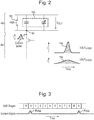
- FIG. 2 is a schematic diagram useful for understanding the principle of operation of ADC banks 48.
- ADC circuitry 48 represents only the ADC circuitry (sub-ADC unit) required for that particular output. Similar ADC circuitry 48 (sub-ADC units) may be provided for all the outputs of the demultiplexers 46.
- ADC circuitry 48 generally takes the form of a capacitance 150.
- capacitance 150 may be variable in value, such that its value can be trimmed during calibration or during an initial setup phase.
- the voltage V OUT for a particular pulse is held across capacitance 150 until the circuitry 48 is reset by reset switch 152. Whilst the voltage V OUT for a particular pulse is held, this analog output value can be converted into a digital output value, for example using an ADC circuit employing a successive-approximation register (SAR).
- SAR successive-approximation register
- each V OUT will have its complementary V OUT , and the pair may be applied together to a differential comparator so that a single digital output for that pair is output.
- An advantage of this mode of operation is that even if delays are experienced within the demultiplexers 46, the charge in each pulse will still make it to the relevant outputs, albeit over a slightly longer period. In that case, the voltage V OUT produced from the pulse remains unaffected.
- the first pulse 154 represents a case in which minimal delay is experienced.
- the second pulse 156 represents a case in which some delay/spreading is experienced, for example due to track capacitance in the circuitry. Consequently, pulse 156 is stretched in time as compared to pulse 154.
- the area of the two pulses 154 and 156 is substantially the same, and thus the output voltage V OUT would be the same for both.
- FIG 3 is a schematic diagram useful for understanding a possible application of SAR - ADC (Successive Approximation Register - Analogue-to-Digital Conversion) circuitry within each sub-ADC unit of the circuitry 48 in Figure 1 .
- Such circuitry could have a cycle of sub-conversion operations (phases/steps) of the form: Reset (R); Sample (S); 1; 2; 3; 4; 5; 6; 7 and 8, as shown in Figure 3 .
- a current pulse concerned may be converted into an output voltage V OUT , and subsequently that voltage V OUT may be turned into an 8-bit digital value over the following 8 SAR sub-conversion operations.
- the next Reset sub-conversion operation then prepares the circuitry for the next current pulse.
- Figure 4 presents example SAR ADC circuitry which may be employed with the circuitry of Figures 1 and 2 , i.e. as part of the sub-ADC units of the ADC banks 48, merely by way of further introduction to the general concept or SAR conversion.
- the main elements are an S/H (Sample/Hold - or sampler) circuit 170 to acquire V OUT from Figure 2 , a voltage comparator 180, an internal DAC 190 and an SAR 200.
- S/H Sample/Hold - or sampler
- the DAC 190 being a capacitive DAC or CDAC
- some of the functionality of the elements e.g. the S/H 170
- may be provided as part of the functionality of another element e.g. the DAC 190.
- the comparator 180 compares the held V OUT with the output of the internal DAC 190 and outputs the result of the comparison to the SAR 200.
- the SAR 200 is designed to supply a digital code approximating to the internal DAC 190.
- the DAC 190 supplies the comparator with an analogue voltage based upon the digital code input from the SAR 200.
- the SAR 200 is initialised so that its MSB is equal to digital 1 (the other bits being digital 0). This code is then input to DAC 190, whose output analogue voltage is supplied to comparator 180. If this analogue voltage is greater than V OUT the comparator 180 causes SAR 200 to reset this bit; otherwise, the bit is kept as a 1. Then, the next bit is set to 1 and the same procedure (sub-conversion operation) is followed, continuing this binary search until every bit in the SAR 200 has been tested (these "tests" corresponding respectively to sub-conversion operations 1 to 8 in Figure 3 ). The resulting digital code output from the SAR 200 is the digital approximation of the sample voltage VOUT and is finally output when the conversion is complete.
- each such “test” involves a comparison operation performed by the comparator.
- sub-conversion operations are carried out synchronously, i.e. with each sub-conversion operation taking the same amount of time as regulated by a clock signal. This may mean that each sub-conversion has a “compare” period during which the necessary comparison is carried out, and at the end of which the result of the comparison is delivered to the surrounding circuitry. This "compare” period may then be followed by a “reset” period in which the comparator is readied for the next comparison, i.e. the next sub-conversion operation.
- asynchronous control is also envisaged, where each successive sub-conversion operation is triggered by the completion of the preceding sub-conversion operation (effectively, by an asynchronous clock signal).
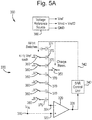
- Figure 5A is a schematic diagram of example SAR ADC circuitry 300 considered by the present inventors.
- the ADC circuitry 300 comprises an analogue input terminal 310, a comparator 320 and successive-approximation control circuitry (which may be referred to simply as successive-approximation circuitry) 330. Also shown is a voltage reference source 380 which may be considered part of the successive-approximation control circuitry or generally part of the SAR ADC circuitry 300.
- the analogue input terminal 310 is connected to receive an analogue input voltage signal V IN (which may correspond to a charge pulse taken from an input control signal in line with Figures 1 and 2 ).
- V IN in Figure 5A may correspond to V OUT in Figures 2 and 4 .
- the comparator 320 has first and second comparator-input terminals 322 and 324 and a comparator-output terminal 326, and is operable to generate a comparison result (e.g. a logic 1 or 0) at its comparator-output terminal 326 based on a potential difference applied across the comparator-input terminals 322 and 324.
- a comparison result e.g. a logic 1 or 0
- the successive-approximation control circuitry 330 is configured to apply a potential difference across the first and second input terminals 322 and 324 based upon the input voltage signal V IN during the sample phase, and configured to control the potential difference for each of a series of successive-approximation operations through charge redistribution as will become apparent, the control applied in each successive-approximation operation being dependent on a comparison result generated by the comparator 320 in the preceding approximation operation.
- the successive-approximation control circuitry 330 comprises a SAR control unit 340, a charge reset switch 350, a plurality of capacitor switches 360 and a corresponding plurality of capacitors 370, and an end capacitor 371.
- the capacitors 370 have first and second capacitor terminals, their first terminals being connected to one of the comparator-input terminals 322 and 324, in this case terminal 324, and their second terminals being connected via respective capacitor switches 360 to the voltage reference source 380.
- each capacitor switch 360 is operable to connect the second terminal of its capacitor 370 to either a V ref voltage supply, a GND voltage supply (i.e.
- the charge reset switch 350 is connected in common to the first terminals of the capacitors 370 and is operable to connect them to e.g. the GND voltage supply (or, in general, some other voltage Vi) effectively to reset the amount of charge stored on the capacitors 370 to a reset or initial amount.
- the SAR control unit 340 is connected to be controlled by the comparison result output from the comparator-output terminal 326 and is configured to control the charge reset switch 350 and the capacitor switches 360 by way of a control signal 342.
- the SAR control unit 340 outputs the eventual digital output value representative of V IN .
- the capacitors 370 in Figure 5A may have for example relative capacitance values 32C, 16C, 8C, 4C, 2C, C from top to bottom, so that their contribution to storing charge (absent any differences between the voltage differences across them) is weighted, in this case using a binary weighting system.
- the end capacitor 371 has its first terminal connected to comparator-input terminal 324 and its second terminal connected to GND.
- the end capacitor has a capacitance value C, such that the total capacitance value (i.e. the sum of the capacitances of the capacitors 370 and the capacitor 371) is 64C, or twice the largest capacitance value of the capacitors 370, 32C.
- the capacitors 370 and 371 could have other capacitance values, and the successive-approximation control circuitry 330 may not comprise the end capacitor 371.
- the end capacitor 371 may be considered optional - removing it simply changes where the step boundaries are (i.e. the voltage steps caused by controlling the switches 360).
- Successive-approximation control circuitry 330 may instead use a non-binary weighting system.
- the capacitors 370 may be given example relative capacitance values 29C, 16C, 9C, 5C, 3C, 2C from top to bottom in Figure 5A .
- the successive-approximation control circuitry 330 employs these relative capacitance values and does not include the capacitor 371.
- the capacitors' 370 contribution to storing charge would be weighted using a non-binary weighting system. That is, 16C is bigger than half of 29C, 9C is bigger than half of 16C, 5C is bigger than half of 9C and so on and so forth.
- An advantage of using a non-binary weighting system is that certain errors in the conversion process (e.g. due to the comparator not settling correctly in time) can be tolerated, and ultimately corrected for.
- the input voltage signal V IN is applied to the comparator-input terminal 322 as shown, the capacitor switches 360 are all controlled to connect the second terminals of their capacitors 370 to V mid , and the charge reset switch 350 is closed to reset the amount of charge stored on the capacitors 370 to an initial amount as mentioned above.
- the capacitors 370 all have the same potential difference across them, and thus the charge stored on them is weighted by their relative capacitance values.
- the charge reset switch 350 is then opened (with the capacitor switches left in their existing state) and the amount of charge on the capacitors 370 is then effectively held with the potential difference between the comparator -input terminals 322 and 324 dependent on V IN (and, indeed, equal to V IN - V 1 ). This is the "start" state.
- the successive-approximation operations then proceed one-by-one, each operation controlling a successive one of the capacitors 370 from the top (largest relative capacitance) to the bottom in Figure 5A .
- the capacitors 370 and capacitor switches 360 will be numbered B1 to B6 from the top to the bottom in Figure 5A , as effectively corresponding to the first to sixth bits (from MSB to LSB) of the eventual (raw) digital output value.
- the successive operations will also be numbered B1 to B6 for similar reasons.
- the top-to-bottom ordering is schematic.
- the comparator 320 outputs a comparison result in the start state. If the result is negative (logic 0), the B1 capacitor switch 360 is switched to GND to cause a -1 ⁇ 2V ref voltage change at the second terminal of the B1 capacitor 370, and the B1 bit of the raw digital output value is assigned value 0. If, however, the result is positive (logic 1), the B1 capacitor switch 360 is switched to V ref to cause a +1 ⁇ 2V ref voltage change at the second terminal of the B1 capacitor 370, and the B1 bit of the raw digital output value is assigned value 1.
- the switching of the B1 capacitor switch 370 causes the (fixed) total amount of charge stored on the capacitors 370 to be redistributed and the voltage level at the comparator-input terminal 324 (and thus the potential difference between the comparator-input terminals 322 and 324) to change accordingly.
- the B2 to B6 capacitor switches 360 are not switched in this operation, and this general idea applies mutatis mutandis to the further operations. The next operation can then begin.
- the comparator In the B2 operation, the comparator outputs a comparison result in the existing state. If the result is negative (logic 0), the B2 capacitor switch 360 is switched to GND to cause a -1 ⁇ 2V ref voltage change at the second terminal of the B2 capacitor 370, and the B2 bit of the raw digital output value is assigned value 0. If, however, the result is positive (logic 1), the B2 capacitor switch 360 is switched to V ref to cause a +1 ⁇ 2V ref voltage change at the second terminal of the B2 capacitor 370, and the B2 bit of the raw digital output value is assigned value 1. Again, the switching of the B2 capacitor switch 370 causes the charge stored on the capacitors 370 to be redistributed. The next operation can then begin.
- the comparator In the B3 operation, the comparator outputs a comparison result in the existing state. If the result is negative (logic 0), the B3 capacitor switch 360 is switched to GND to cause a -1 ⁇ 2V ref voltage change at the second terminal of the B3 capacitor 370, and the B3 bit of the raw digital output value is assigned value 0. If, however, the result is positive (logic 1), the B3 capacitor switch 360 is switched to V ref to cause a +1 ⁇ 2V ref voltage change at the second terminal of the B3 capacitor 370, and the B3 bit of the raw digital output value is assigned value 1. Again, the switching of the B3 capacitor switch 370 causes the charge stored on the capacitors 370 to be redistributed.
- the B4 to B6 operations continue one after the other in the same manner, and duplicate description can be omitted.
- a final comparison can be carried out which may give a 7 th bit (i.e. B7) and thus the raw digital output value, e.g. 1011011, is produced.
- This value is referred to as a "raw” value since there may be some subsequent "correction" of this result in the SAR control unit 340 (or in other circuitry such as a processor connected thereto and not shown in Figure 5 ), in the example in which successive-approximation control circuitry 330 uses a non-binary weighting system as mentioned above to lead to a "corrected" digital output value.
- non-binary weighting system could be applied in Figure 5A with non-binary weighted relative capacitance values (as mentioned above), with the benefit of correction afforded by the non-binary weighting system.
- non-binary maybe considered to mean that each (or at least one) successive value is more than half the previous one from successive operation to operation, so that the ratio R of the values (e.g. 29C/16C in capacitance values, or more importantly 14.5/8 in relative weights) satisfies 1 ⁇ R ⁇ 2 (more generally, R ⁇ 2 or R ⁇ 2).
- the voltage reference source 380 of the successive-approximation control circuitry 330 described above outputs V ref , V mid (V ref /2) and GND (ground).
- successive-approximation control circuitry 330 can also be operated in a different way in which the switches 360 are configured to connect the second terminals of the capacitors 370 to either GND or a reference voltage (e.g. Vref) (and also to the analogue input voltage signal V IN in an initial phase).
- Such successive-approximation control circuitry 330 is operated by first connecting the second terminals of all the capacitors 370 to the analogue input voltage signal V IN with the charge reset switch 350 closed, then the charge reset switch 350 is opened and the second terminals of all the capacitors 370 are disconnected from the analogue input voltage signal V IN , thus effectively trapping a charge proportional to the input voltage in the capacitors 370.
- the second terminals of all the capacitors 370 are then connected to GND, driving the potential at the comparator-input terminal 324 to -V IN .
- the comparator-input terminal 322 is connected to GND.
- the potential difference between the comparator-input terminals 322 and 324 is 0 (ideally).
- the B1 capacitor switch 360 is switched to V ref .
- the potential at the comparator-input terminal 324 is shifted in the positive direction by an amount equal to 1 ⁇ 2 V ref .
- the comparator 320 outputs a comparison result. If the result is negative (logic 0), the B1 capacitor switch 360 is switched to GND and the B1 bit of the raw digital output value is assigned value 0. If, however, the result is positive (logic 1), the B1 capacitor switch 360 is not switched (that is, is stays connected to V ref ) and the B1 bit of the raw digital output value is assigned value 1.
- the B2 capacitor switch 360 is switched to V ref and the comparator outputs a comparison result. Again, if the result is negative (logic 0), the B2 capacitor switch 360 is switched to GND and the B2 bit of the raw digital output value is assigned value 0, and if, however, the result is positive (logic 1), the B2 capacitor switch 360 is not switched (that is, is stays connected to V ref ) and the B2 bit of the raw digital output value is assigned value 1.
- the B3 to B6 operations in this implementation continue one after the other in the same manner and duplicate description can be omitted.
- a final comparison can be carried out which may give a 7 th bit (i.e. B7) and thus the raw digital output value, e.g. 1011011, is produced.
- the raw digital output value e.g. 1011011
- each switch 360 may be configured to switch between V ref , V mid and GND, or between V ref , GND and V IN , depending on how the successive-approximation control circuitry 330 is to be operated.
- the array of capacitors 370 and capacitor switches 360 may be referred to as a CDAC (capacitive DAC).
- controllable voltage-signal generation circuitry comprising: a plurality of segment nodes connected together in series, each adjacent pair of segment nodes in the series connection being connected together via a corresponding coupling capacitor, an end one of the segment nodes in the series connection serving as (or being) an output node; for each of the segment nodes, at least one segment capacitor having first and second terminals, the first terminal connected to that segment node and the second terminal connected to a corresponding switch; and switch control circuitry, wherein: each switch is operable to connect the second terminal of its segment capacitor to one reference voltage source and then instead to another reference voltage source, those reference voltage sources having different voltage levels, to apply a voltage change at the second terminal of its segment capacitor; the reference voltage sources and switches are configured such that for each segment node the same voltage change in magnitude is applied by each switch of that segment node, and such that the voltage change applied by each switch of one segment node is different in magnitude from the voltage change applied by each switch of another segment no
- Such circuitry enables a voltage signal to be generated based on the control of the switches. Such circuitry enables accurate control of the output voltage signal to be achieved in the sense that parasitic capacitances in the circuitry may be compensated for by setting the voltage changes appropriately (i.e. different from other voltage changes in some cases).
- Such circuitry also enables accurate control of the output voltage signal to be achieved with fewer and/or smaller capacitors, in comparison to a case in which one or more banks of capacitors are used to compensate for parasitic capacitances in the circuitry. Since such banks of capacitors may not be required, a reduction in area of the circuitry may be achieved. A voltage change in the sense that it is used above may be readily adjusted, so the controllable voltage-signal generation circuitry makes it easier to compensate for parasitic capacitances by calibration (for example performed during an initial start-up phase, or during operation), especially since such parasitic capacitances may be incorrectly estimated during circuit design.
- Such circuitry also enables accurate control of the output voltage signal to be achieved with fewer practical restrictions on the coupling capacitors, since the voltage change applied by each switch of one segment node is different in magnitude from the voltage change applied by each switch of another segment node. That is, the voltage changes may be set so that the restrictions on the values of the coupling capacitors may be relaxed.
- the controllable voltage-signal generation circuitry may be implemented within or considered to be a CDAC, which may further be implemented within a SAR ADC, as disclosed herein. That is, the switches may be controlled based on a digital signal (an input word or code).
- the plurality of segment nodes may comprise at least three segment nodes.
- at least two or three said segment capacitors may be connected at their first terminals to that segment node and at their second terminals to corresponding said switches, the capacitances of those segment capacitors optionally being binary-weighted relative to one another.
- the capacitances may be binary-weighted relative to one another in the sense that they follow a binary weighting system as described above with reference to Figures 5A and 5B .
- the plurality of segment nodes may comprise at least three segment nodes.
- the reference voltage sources and switches may be configured such that, for at least three said segment nodes, the voltage change applied by each switch of any one of those segment nodes is different in magnitude from the voltage change applied by each switch of the other segment nodes of those segment nodes. That is, for at least three segment nodes, the corresponding voltage changes may be different one another.
- the voltage changes may be set to compensate for parasitic capacitances in the circuitry, and/or to relax the requirements on the coupling capacitors, for example.
- At least one of said reference voltage sources may be a variable reference voltage source configured to be adjusted to adjust the voltage change applied by each switch connected to that reference voltage source.
- the voltage change or changes concerned may thereby be adjusted during operation or in an initial start-up phase of the circuitry.
- At least one said reference voltage source connected to each switch may be a variable reference voltage source configured to be adjusted to adjust the voltage change applied by each switch concerned.
- the controllable voltage-signal generation circuitry may comprise calibration circuitry configured to adjust the voltage level of at least one of the reference voltage sources.
- Calibration may be performed during operation or in an initial start-up phase of the controllable voltage-signal generation circuitry. Such calibration may be performed in order to compensate for parasitic capacitances in the circuitry, and/or to relax the requirements on the coupling capacitors, for example.
- the calibration circuitry may be configured to adjust the voltage level of at least one of the reference voltage sources connected to each switch for the segment node serving as (or being) the output node so as to adjust the voltage change applied by each switch of that segment node.
- the calibration circuitry may be configured to adjust the voltage change applied by each switch of the segment node serving as the output node to calibrate out a gain error of the controllable voltage-signal generation circuitry (or to set the correct gain of, or control the gain of, the controllable voltage-signal generation circuitry).
- the calibration circuitry may be configured to adjust the voltage level of at least one of the reference voltage sources connected to each switch for at least one segment node other than the segment node serving as the output node so as to adjust the voltage change applied by each switch of that segment node.
- the calibration circuitry may be configured to adjust the voltage change applied by each switch of at least one segment node other than the segment node serving as the output node together with (i.e. by the same amount as) the voltage change applied by each switch of the segment node serving as the output node to calibrate out a gain error of the controllable voltage-signal generation circuitry (or to set the correct gain of, or control the gain of, the controllable voltage-signal generation circuitry).
- the calibration circuitry may be configured to adjust the voltage change applied by each switch of each segment node other than the segment node serving as the output node together with (i.e. by the same amount as) the voltage change applied by each switch of the segment node serving as the output node to calibrate out a gain error of the controllable voltage-signal generation circuitry (or to set the correct gain of, or control the gain of, the controllable voltage-signal generation circuitry).
- the reference voltage sources may be connected to the switches such that adjusting the voltage level of said at least one of the reference voltage sources connected to each switch for said at least one segment node other than the segment node serving as the output node adjusts the voltage change applied by each switch of that segment node: independently of the voltage change applied by each switch of each other segment node; and/or relative to the voltage change applied by each switch of the segment node serving as the output node.
- the calibration circuitry may be configured to adjust the voltage change applied by each switch of at least one segment node other than the segment node serving as the output node to calibrate out non-linearity errors caused by the controllable voltage-signal generation circuitry.
- the calibration circuitry may be configured to adjust the voltage change applied by each switch of at least one segment node other than the segment node serving as the output node to adjust a weighting of the effect of the voltage changes for that segment node relative to a weighting of the effect of the voltage changes for another said segment node.
- the controllable voltage-signal generation circuitry may be a CDAC, the switch control circuitry configured to control the switches in dependence upon a digital signal; and/or for each segment node, that segment node, the connected at least one segment capacitor and corresponding switch, and a corresponding part of the switch control circuitry for controlling each of those switches may constitute a CDAC, the switch control circuitry configured to control those switches in dependence upon a digital signal.
- each segment capacitor may correspond to a bit of the digital signal (the input word or code).
- digital-to-analogue converter circuitry or analogue-to-digital converter circuitry comprising the controllable voltage-signal generation circuitry of the aforementioned first aspect of the present invention.
- the switch control circuitry may be configured to control the switches in dependence upon a digital signal.
- that circuitry may comprise such digital-to-analogue converter circuitry.
- each segment capacitor may correspond to a bit of the digital signal (the input word or code).
- analogue-to-digital converter circuitry comprising: an analogue input terminal, operable to receive an analogue input voltage signal; a comparator having first and second comparator-input terminals and operable to generate a comparison result based on a potential difference applied across those terminals; and successive-approximation control circuitry configured to apply a potential difference across the first and second comparator-input terminals based upon the input voltage signal, and configured to control the potential difference for each of a series of successive approximation operations (through charge redistribution), the control applied in each successive approximation operation being dependent on a comparison result generated by the comparator in the preceding approximation operation, wherein: the successive-approximation control circuitry comprises the controllable voltage-signal generation circuitry of the aforementioned first aspect of the present invention; and the switch control circuitry is configured to control the switches in each successive approximation operation in dependence upon the comparison result generated by the comparator in
- the reference voltage sources may be configured so that a non-binary search is performed by the series of successive approximation operations, the search being non-binary in that across the series of successive approximation operations the search or search range from one approximation operation to the next in at least one instance is weighted between 2:1 and 1:1.
- the reference voltage sources may be configured so that the non-binary search is non-binary in that across the series of successive approximation operations the search or search range from one approximation operation to the next in at least one instance is weighted (1/ ⁇ 2):1.
- integrated circuitry such as an IC chip, comprising the controllable voltage-signal generation circuitry of the aforementioned first aspect of the present invention, or the digital-to-analogue converter circuitry or analogue-to-digital converter circuitry of the aforementioned second aspect of the present invention, or the analogue-to-digital converter circuitry of the aforementioned third aspect of the present invention.
- the present disclosure extends to method aspects corresponding to the apparatus (circuitry) aspects.
- FIG. 6 is a schematic diagram of controllable voltage-signal generation circuitry 400 according to the present invention.
- the controllable voltage-signal generation circuitry 400 shown in Figure 6 could be implemented in a SAR ADC (for example it could replace the capacitors 370 and 371 and switches 360 in Figure 5A , and the node 403 could be connected to the comparator-input terminal 324).
- Controllable voltage-signal generation circuitry 400 comprises a plurality of segment nodes 401, 402 and 403, a plurality of segment capacitors 470, an (optional) end capacitor 471, a plurality of switches 460, a plurality of coupling capacitors 472 and voltage sources 10, 20 and 30.
- the controllable voltage-signal generation circuitry 400 shown in Figure 6 also comprises calibration circuitry 490.
- calibration circuitry 490 is not essential and in implementations other than the one shown in Figure 6 controllable voltage-signal generation circuitry 400 does not comprise calibration circuitry 490.
- Segment nodes 401, 402 and 403 are connected together in series. Each adjacent pair of segment nodes 401, 402 and 403 are connected together via a corresponding coupling capacitor 472. Segment node 403 serves as an output node.
- the segment capacitors 470 are grouped into segments 411, 412 and 413, with three segment capacitors 470 per segment. Segment nodes 401, 402 and 403 correspond respectively to segments 411, 412 and 413, and voltage sources 10, 20 and 30 correspond respectively to segments 411, 412 and 413.
- Each segment capacitor 470 comprises first and second terminals.
- the first terminal of each segment capacitor 470 is connected to the segment node 401, 402 and 403 corresponding to the segment 411, 412 and 413 to which that segment capacitor belongs.
- the second terminal of each segment capacitor 470 is connected to the voltage source 10, 20 and 30 corresponding to the segment 411, 412 and 413 to which that segment capacitor 470 belongs.
- the second terminal of each segment capacitor 470 is connected to the corresponding voltage source 10, 20 and 30 via a switch 460.
- the end capacitor 471 comprises first and second terminals, the first terminal connected to the segment node 401 and the second terminal connected to ground (GND), as an example voltage source.
- the controllable voltage-signal generation circuitry 400 may not comprise the end capacitor 471. As above, omitting the end capacitor 471 adjusts the step boundaries (i.e. the voltage steps caused by switching the switches 460).
- the pairs of segment capacitors 470 and switches 460 are labelled from D ⁇ 0> to D ⁇ 8>. Such labelling can aid understanding in the context of the controllable voltage-signal generation circuitry 400 being used in or as a DAC such as a CDAC (and further in a SAR ADC), where the switches 460 are controlled according to the bits of a binary word such as a binary input word (comprising, in the case of the controllable voltage-signal generation circuitry 400 shown in Figure 6 , 9 bits, i.e. D ⁇ 0> to D ⁇ 8>; in that case, segment 413 can be referred to as the MSB (most significant bit) segment and segment 411 can be referred to as the LSB (least significant bit) segment).
- Each voltage source 10, 20 and 30 is operable to supply two or more reference voltages (and thus may be considered to comprise two or more reference voltage sources) so that each switch 460 can be switched to effect a change in the voltage supplied to the second terminal of its corresponding segment capacitor 470. That is, the voltage sources 10, 20 and 30 are operable, in combination with the switches 460 of the corresponding segments 411, 412 and 413, to effect voltage changes ⁇ V1, ⁇ V2 and ⁇ V3, respectively.
- the voltage sources 10, 20 and 30 and their connection to the second terminals of the segment capacitors 470 via the switch 460 are described in more detail below with reference to Figure 7 .
- the controllable voltage-signal generation circuitry 400 shown in Figure 6 is segmented using the coupling capacitors 472 to scale the relative contribution (to the voltage at the output node 403) provided by each segment 411, 412 and 413.
- the segment capacitors 470 in each segment 411, 412 and 413 have values so that their relative contribution (to the voltage at the output node 403) is scaled.
- each segment 411, 412 and 413 comprises three segment capacitors 470 with respective capacitances of C, 2C and 4C, and the coupling capacitors 472 each have a capacitance of 8/7 C.
- the contribution to the voltage at the output node 403 is equivalent to or the same as would be the case were the segment capacitors 470 starting from the left and moving right across Figure 6 to have respective capacitances of 256C, 128C, 64C, 32C, 16C, 8C, 4C, 2C and C (i.e. binary weighted), with the coupling capacitors 472 omitted (i.e. shorting nodes 401, 402, 403 together).
- Calibration circuitry 490 is connected to receive measurement information and to output control signals S1, S2 and S3 in order to control the voltage sources 10, 20 and 30, respectively. Calibration circuitry 490 is explained in more detail below.
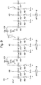
- FIGS 7A and 7B are schematic diagrams showing how the voltage sources 10, 20 and 30 may be connected with the switches 460 in Figure 6 . Only the voltage source 30 is shown, but the other voltage sources 10 and 20 may be connected in the same basic way.
- An implementation of controllable voltage-signal generation circuitry 400 using such a connection between the voltage sources 10, 20 and 30 and the switches 460 could be used in the first implementation described above with reference to Figures 5A and 5B (i.e. the implementation in which each switch 360 is configured to switch between for example V ref , V mid and GND).
- FIG 7B shows an example of the connection between voltage source 30 and a switch 460 in an implementation in which each switch 470 of controllable voltage-signal generation circuitry 400 shown in Figure 6 is operable to connect the second terminal of its segment capacitor either to a first reference voltage source Vref3' or a second reference voltage source Vref3.
- An implementation of controllable voltage-signal generation circuitry 400 using such a connection between the voltage sources 10, 20 and 30 and the switches 460 could be used in the second implementation described above with reference to Figures 5A and 5B (i.e. the implementation in which each switch 360 is configured to switch between V ref and GND (and V IN , for the purpose of charging the capacitors, although not shown in Figure 7B ).
- the voltage change ⁇ V2 applied by each switch 460 of segment 412 is 1 ⁇ 2 * (Vref2 - Vref2') and the voltage change ⁇ V1 applied by each switch 460 of segment 411 is 1 ⁇ 2 * (Vref1 - Vref1').
- the voltage change ⁇ V3 is (Vref3 - Vref3'), since each switch of the segment 413 switches the connection of the second terminal of its segment capacitor 470 from Vref3 to Vref3' (or vice versa ) to effect the voltage change.
- the voltage change ⁇ V2 is (Vref2 - Vref2') and the voltage change ⁇ V1 is (Vref1 - Vref1').
- one of the reference voltage sources Vref3 and Vref3' and Vmid3 is simply ground (GND).
- GND ground
- one of the reference voltage sources Vref1, Vref1' and Vmid1 may be ground (GND)
- one of the reference voltage sources Vref2, Vref2' and Vmid2 may be ground (GND).
- the voltage sources 10, 20, and 30 may be configured such that the voltage changes ⁇ V1, ⁇ V2 and ⁇ V3 are variable and not necessarily equal to one another.
- the reference voltage sources Vref1 or Vref1' (and therefore Vmid1 by extension, as the case may be) is variable.
- the values for the reference voltage sources Vref1, Vref1', Vref2, Vref2', Vref3 and Vref3' may be selected in order to control the relative scaling between segments 411, 412 and 413 of controllable voltage-signal generation circuitry 400. That is, those values may be chosen to compensate for parasitic capacitances and other sources of error/mismatch, as will be described in more detail below.
- the reference voltage sources and switches 460 are configured such that for each segment node 401, 402 and 403 the same voltage change ⁇ V1, ⁇ V2 and ⁇ V3 in magnitude is applied by each switch 460 of that segment node 401, 402 and 403.
- the reference voltage sources 10, 20 and 30 and switches 460 are configured such that also, for each segment node 401, 402 and 403, the voltage change ⁇ V1, ⁇ V2 and ⁇ V3 applied by each switch 460 of one segment node 401, 402 and 403 is different in magnitude from the voltage change ⁇ V1, ⁇ V2 and ⁇ V3 applied by each switch 460 of another segment node 401, 402 and 403.
- the voltage changes ⁇ V1, ⁇ V2 and ⁇ V3 may be chosen such that one of them is different whilst all of the others are the same, or so that a number of them are different from a number of others but the same as each other (in magnitude).
- the voltage changes ⁇ V1, ⁇ V2 and ⁇ V3 may also be chosen so that they are each different in magnitude.
- the voltage changes ⁇ V1, ⁇ V2 and ⁇ V3 may be chosen and set before shipping, or may be designed in (so that the voltage sources 10, 20, and 30 are not or need not be variable), or they may be chosen and set during operation of the controllable voltage-signal generation circuitry 400.
- the voltage changes ⁇ V1, ⁇ V2 and ⁇ V3 may be continually adjusted during operation of the controllable voltage-signal generation circuitry 400.
- the voltage changes ⁇ V1, ⁇ V2 and ⁇ V3 may be chosen/set/adjusted through a calibration process.
- the voltage changes ⁇ V1, ⁇ V2 and ⁇ V3 may be controlled by calibration circuitry 490 shown in Figure 6 .
- This control may be performed before shipping, or during operation (for example it may be performed at startup, continually or at regular intervals during operation).
- Calibration circuitry 490 may receive measurement information in the form of the voltage levels at one or more segment nodes 401, 402 and 403, and/or in the form of measurement values of effective capacitances at various positions in controllable voltage-signal generation circuitry 400, and/or as other information (e.g. gain/error information) which may be provided based on external measurements.
- Calibration circuitry 490 as shown in Figure 6 is configured to output control signals S1, S2 and S3 in order to control voltage changes ⁇ V1, ⁇ V2 and ⁇ V3, respectively. However calibration circuitry 490 may output more or fewer control signals. For example in other implementations calibration circuitry 490 is configured to output only one control signal to control one or more of the voltage changes ⁇ V1, ⁇ V2 and ⁇ V3, or any number of control signals to control any number of the voltage changes ⁇ V1, ⁇ V2 and ⁇ V3. In other implementations calibration circuitry 490 is configured to output one control signal to control a reference voltage source (e.g. Vref3) and another control signal to control another reference voltage source of the same voltage source 10, 20 and 30 (e.g. Vref3').
- Vref3 reference voltage source
- FIG 8A is a schematic diagram of controllable voltage-signal generation circuitry 400 useful for understanding the present invention, in particular the choice of the voltage changes ⁇ V1, ⁇ V2 and ⁇ V3.
- the controllable voltage-signal generation circuitry 400 is shown in Figure 8A along with a capacitor, Ccomp, 473 to assist in understanding.
- the capacitor Ccomp 473 represents a parasitic capacitance experienced at the output node 403 of the controllable voltage-signal generation circuitry 400 (when the controllable voltage-signal generation circuitry 400 is implemented as part of a CDAC in successive-approximation control circuitry like the successive-approximation control circuitry 330 of Figure 5A , the capacitor Ccomp 473 represents a parasitic capacitance at the input of the comparator 320).
- the parasitic capacitance represented by Ccomp 473 causes a full-scale gain error as the output of the controllable voltage-signal generation circuitry 400 (i.e. the output at output node 403) gets attenuated by the parasitic capacitance represented by Ccomp 473. That is, the parasitic capacitance represented by Ccomp 473 results in a voltage division occurring between the effective capacitance of the controllable voltage-signal generation circuitry 400 and Ccomp 473.
- This full-scale gain error causes a drop in the overall resolution of for example a CDAC in which the controllable voltage-signal generation circuitry 400 is implemented, as full-scale signal level drops (i.e. there is an overall drop in SNR (signal-to-noise ratio)).
- the full-scale gain error caused by the parasitic capacitance represented by Ccomp 473 can be corrected for (i.e. cancelled out at least partially, or minimised) by adjusting the voltage change ⁇ V3 applied to the second terminals of the segment capacitors 470 of segment 403 by the corresponding respective switches 460 (that is, by adjusting the voltage change corresponding to the output node 403).
- the voltage source 30 is illustrated as a variable voltage source to indicate that the voltage change ⁇ V3 can be varied in this running example.
- the voltage sources 10, 20 and 30 and the switches 460 are configured as described with reference to Figures 7A and 7B , with one or more of the reference voltage sources Vref3, Vref3' and Vmid3 being variable in order to effect the voltage change ⁇ V3, but the voltage source 30 is illustrated in a simpler form in Figure 8A to aid overall understanding.
- the voltage change ⁇ V3 may be controlled/adjusted in order to mitigate the effects of the parasitic capacitance represented by Ccomp 473 at the output node 403.
- Ccomp 473 the effective capacitance represented by Ccomp 473 at the output node 403.
- the effective capacitance C eff looking into the controllable voltage-signal generation circuitry 400 from the output node 403 is 8C. If, for example, the unit capacitance represented by C is taken to be 12.5 fF, then the effective capacitance C eff is 100 fF.
- the parasitic capacitance represented by Ccomp 473 can be estimated in this example to be 40 fF (this value could for example be calculated/measured by calibration circuitry 490, or calibration circuitry 490 may make small corrections iteratively to gradually cancel out this parasitic capacitance), meaning that the overall transfer function of the controllable voltage-signal generation circuitry 400 is attenuated due to this parasitic capacitance by 40%. Therefore in order to compensate for the 40% attenuation a 40% increase in the voltage change ⁇ V3 is required (for example in order to maintain a ⁇ 250 mV peak-to-peak output (at the output node 403) the voltage change ⁇ V3 should be increased in magnitude to 350 mV). As explained below, the voltage changes ⁇ V1 and ⁇ V2 may be adjusted together with the voltage change ⁇ V3.
- control of the voltage change ⁇ V3 may be performed by calibration circuitry 490, or may be performed by other circuitry not comprised within controllable voltage-signal generation circuitry 400.
- Figure 8B is a graph illustrating the transfer function of a 9-bit CDAC comprising the controllable voltage-signal generation circuitry 400 when the voltage changes ⁇ V1, ⁇ V2 and ⁇ V3 are all set to 250 mV (the circles in Figure 8B ) and when the voltage changes ⁇ V1, ⁇ V2 and ⁇ V3 are all set to 350 mV (the crosses in Figure 9B ).
- the peak-to-peak output (at the output node 403) is roughly 175 mV in the case that the voltage changes ⁇ V1, ⁇ V2 and ⁇ V3 are all set to 250 mV due to the parasitic capacitance represented by Ccomp 473.
- the peak-to-peak output (at the output node 403) is roughly 246 mV in the case that the voltage changes ⁇ V1, ⁇ V2 and ⁇ V3 are all set to 350 mV in order to compensate for the parasitic capacitance represented by Ccomp 473.
- all of the voltage changes ⁇ V1, ⁇ V2 and ⁇ V3 have been changed, but in other implementations only the voltage change ⁇ V3 is changed. Also, in other implementations some but not all of the voltage changes other than the voltage change corresponding to the output node 403 (i.e. the voltage change ⁇ V3) may be changed together with the voltage change corresponding to the output node 403.
- FIG 9 is a schematic diagram of controllable voltage-signal generation circuitry 400 useful for understanding the present invention, in particular the choice of the voltage changes ⁇ V1, ⁇ V2 and ⁇ V3.
- the controllable voltage-signal generation circuitry 400 is shown in Figure 9 along with capacitors Cpa and Cpc 474 which represent parasitic capacitances across the coupling capacitors 472 (top and bottom plate parasitic capacitances across the coupling capacitors 472, and between any metal routing around the coupling capacitors 472).
- the controllable voltage-signal generation circuitry 400 is also shown in Figure 9 along with capacitors Cpb and Cpd 475 which represent parasitic capacitances to the substrate across the coupling capacitors 472 (i.e. between the coupling capacitors 472 and ground).
- the parasitic capacitances represented by capacitors Cpa and Cpc effectively increase the capacitances of the coupling capacitors 474, thereby decreasing the weights of individual segments (the segments 411 and 412 - i.e. segments other than the segment 413 corresponding to the output node 403).
- the parasitic capacitances represented by capacitors Cpb and Cpd further attenuate the weights of individual segments (the segments 411 and 412 - i.e. segments other than the segment 413 corresponding to the output node 403) as these parasitic capacitances are seen in parallel to the segment capacitors 470.
- the segment 413 corresponding to the output node 403 is loaded by subsequent segments (i.e. the other segments 411 and 412).
- the parasitic capacitances represented by Cpa, Cpb, Cpc and Cpd 474 and 475 cause non-linearities or non-linearity errors (across the transfer characteristics of the CDAC implementation of controllable voltage-signal generation circuitry 400) such as DNL (differential non-linearity) errors and INL (integral non-linearity) errors as they change the weighting of segment capacitors 470 compared to segment capacitors 470 of other segments.
- the DNL and INL errors result in the degradation of the SNR (signal-to-noise ratio) which in turn degrades the ENOB (effective number of bits) of for example a CDAC in which the controllable voltage-signal generation circuitry 400 is implemented.
- the parasitic capacitances represented by capacitors Cpa, Cpb, Cpc and Cpd 474 and 475 can be corrected for (i.e. cancelled out at least partially, or minimised) by adjusting either or both of the voltage changes ⁇ V1 and ⁇ V2 (applied to the second terminals of the segment capacitors 470 of segments 401 and 402 by the corresponding respective switches 460) relatively to each other and the voltage change ⁇ V3 (that is, by adjusting the voltage change corresponding to one or more of the segment nodes 401 and 402 other than the output node 403, relatively to each other and to the voltage change ⁇ V3 corresponding to the output node 403).
- the variability of the voltage changes ⁇ V1 and ⁇ V2 is being illustrated in Figure 9 in particular, however the other voltage source 30 and the other voltage change ⁇ V3 are shown, for completeness (the voltage change ⁇ V3 may have been previously adjusted to first calibrate out a gain error for example).
- the voltage sources 10 and 20 are illustrated as variable voltage sources to indicate that the voltage changes ⁇ V1 and ⁇ V2 can be varied in this running example.
- the voltage sources 10, 20 and 30 and the switches 460 are configured as described with reference to Figures 7A and 7B , with one or more of the reference voltage sources Vref1, Vref1' and Vmid1 being variable in order to effect the voltage change ⁇ V1, and one or more of the reference voltage sources Vref2, Vref2' and Vmid2 being variable in order to effect the voltage change ⁇ V2, but the voltage sources 10 and 20 are illustrated in a simpler form in Figure 9 to aid overall understanding.
- the voltage changes will get successively larger moving from the MSB segment down to the LSB segment.
- one or more of the voltage changes ⁇ V1 and ⁇ V2 may be controlled/adjusted in order to mitigate the effects of the parasitic capacitances represented by capacitors Cpa, Cpb, Cpc and Cpd 474 and 475.
- one or more of the voltage changes ⁇ V1 and ⁇ V2 may be changed relatively to the voltage change ⁇ V3 (and also relatively to each other) in order to adjust the effective weighting of segment capacitors 470 of one or more of the segments 411 and 412 corresponding to the voltage changes ⁇ V1 and ⁇ V2 relatively to segment capacitors 470 of the segment 413 corresponding to the voltage change ⁇ V3 and to the output node 403 (and also relatively to segment capacitors 470 of the other segments 411 and 412).
- parasitic capacitances described above with reference to Figures 8 and 9 are merely examples of the kind of parasitic capacitances that can be corrected for in the controllable voltage-signal generation circuitry 400.
- any parasitic capacitances can be corrected for (e.g. through trial and error or through calculation of the parasitic capacitance), for example systematic layout parasitics which occur between segments 411, 412 and 413.
- the voltage changes ⁇ V1 and ⁇ V2 are controlled to be changed by the same amount so that they are equal (in magnitude) to each other (this for example ignores particular systematic and layout parasitic capacitances).
- the switches 460 may be switched so that they correspond to an input word (a code) consisting entirely of zeroes (i.e. full scale in one direction, so that D ⁇ 0> to D ⁇ 8> are all logic 0) and the voltage level at the output node 403 measured, and then the switches 460 may be switched so that they correspond to an input word consisting entirely of ones (i.e. full scale in the other direction, so that D ⁇ 0> to D ⁇ 8> are all logic 1) and the voltage level at the output node 403 measured again. The difference between these two voltage levels (i.e.
- controllable voltage-signal generation circuitry 400 may be compared against a preferred or reference voltage swing value and one or more of the voltage changes ⁇ V1, ⁇ V2 and ⁇ V3 (at least ⁇ V3) may be adjusted to bring the measured voltage swing to or towards the preferred reference voltage swing value, i.e. to adjust the gain.
- the switches 460 may be switched in a manner so that, effectively, all possible "codes" are supplied to the controllable voltage-signal generation circuitry 400, successively (i.e. the switches 460 may be operated so that the voltage level at the output node 403 increases successively with each successive operation of the switches 460, i.e. from full scale in one direction to full scale in the other).
- the voltage level at the output node 403 may then be measured after each switch operation.
- Such an operation may be referred to as a "code sweep”.
- One or more of the voltage changes ⁇ V1, ⁇ V2 and ⁇ V3 may be adjusted (e.g. to calibrate out non-linearities corresponding to Cpa, Cpb, Cpc and Cpd in Figure 9 ) and the code sweep repeated in order to determine whether the adjustment has had the desired effect.
- the voltage change ⁇ V3 is adjusted during a first stage in which the gain of controllable voltage-signal generation circuitry 400 is calibrated. Then the voltage changes ⁇ V1 and ⁇ V2 are adjusted during a second stage (calibration to mitigate non-linearity errors). In another implementation, the voltage changes ⁇ V1 and ⁇ V2 may be adjusted together with ⁇ V3 in the first stage. Of course, in other implementations the first and second stages may be performed in a different order, and repeated successively until a desired performance is achieved.
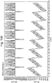
- Figure 10A shows graphs representing the DNL and the INL for an implementation of controllable voltage-signal generation circuitry 400 in which each of the voltage changes ⁇ V1, ⁇ V2 and ⁇ V3 is equal in magnitude to 350 mV.
- Figure 10B shows graphs representing the DNL and the INL for an implementation of controllable voltage-signal generation circuitry 400 in which the voltage change ⁇ V3 is equal in magnitude to 350 mV and each of the voltage changes ⁇ V1 and ⁇ V2 is equal in magnitude to 359 mV. It can be seen from these graphs that the DNL and INL are smaller in magnitude when the voltage changes ⁇ V1 and ⁇ V2 have been adjusted to mitigate the effects of parasitic capacitances.
- Figure 11A shows graphs representing the DNL and the INL for an implementation of controllable voltage-signal generation circuitry 400 in which each of the voltage changes ⁇ V1, ⁇ V2 and ⁇ V3 is equal in magnitude to 350 mV.
- Figure 11B shows graphs representing the DNL and the INL for an implementation of controllable voltage-signal generation circuitry 400 in which the voltage change ⁇ V3 is equal in magnitude to 350 mV and each of the voltage changes ⁇ V1 and ⁇ V2 is equal in magnitude to 363.5 mV. It can be seen from these graphs that the DNL and INL are smaller in magnitude when the voltage changes ⁇ V1 and ⁇ V2 have been adjusted to mitigate the effects of parasitic capacitances.
- the graphs shown in Figures 11A and 11B have been generated based on extracted simulations of the controllable voltage-signal generation circuitry 400.
- parasitic capacitances due to the layout of the circuitry are also included (i.e. the extracted simulations include the parasitic capacitances associated with the components themselves and also the parasitic capacitances due to the interconnections, for example).
- controllable voltage-signal generation circuitry 400 Aside from the calibration and correction for parasitic capacitances described above, there are other additional benefits to the controllable voltage-signal generation circuitry 400.
- controllable voltage-signal generation circuitry 400 when the controllable voltage-signal generation circuitry 400 is implemented as part of a CDAC, it is capable of both binary and non-binary conversion.
- the controllable voltage-signal generation circuitry 400 in a binary implementation the controllable voltage-signal generation circuitry 400 is implemented with the capacitance values for the segment capacitors 470 as shown in Figure 6 , and the voltage changes ⁇ V1, ⁇ V2 and ⁇ V3 could be controlled (taking account of parasitic capacitances) so that the effective relative weights of each segment capacitor 470 as viewed from the output node 403 are (exactly), starting from the left of Figure 6 and moving to the right, 256C, 128C, 64C, 32C, 16C, 8C, 4C, 2C and C. That is, the voltage changes ⁇ V1, ⁇ V2 and ⁇ V3 may be controlled so that the segment capacitors have effectively (exact) binary weighting.
- controllable voltage-signal generation circuitry 400 is implemented still with the capacitance values for the segment capacitors 470 as shown in Figure 6 , but the voltage changes ⁇ V1, ⁇ V2 and ⁇ V3 are controlled relative to one another (such as by controlling ⁇ V1 and/or ⁇ V2 relative to ⁇ V3) so that the relative weights of segment capacitors 470 of one segment overlap with (or are shifted relative to, as compared to the binary weighting situation described above) the relative weighs of segment capacitors 470 of another segment.
- the voltage changes ⁇ V1, ⁇ V2 and ⁇ V3 are controlled so that for example the right-most segment capacitor 470 of segment 412 has an effective weight as viewed from the output node 403 (taking into account the coupling capacitors 472, any parasitic capacitance and the effect of the voltage changes ⁇ V1, ⁇ V2 and ⁇ V3) less than the effective weight of the middle segment capacitor 470 of segment 411 and more than the right-most segment capacitor 470 of the segment 411.
- the same considerations apply to other segment capacitors 470.
- non-binary may refer to any weighting system in which not every step between successive segment capacitors 470 is binary (non-binary here therefore includes weighting systems in which every such step is non-binary).
- controllable voltage-signal generation circuitry 400 Another advantage of the controllable voltage-signal generation circuitry 400 is improved speed. Due to the coupling capacitors 472, the maximum capacitance of a segment capacitor 470 is reduced (e.g. the maximum capacitance of a segment capacitor is 4C in the controllable voltage-signal generation circuitry 400 shown in Figure 6 , but in equivalent circuitry (e.g. suitable for implementation in a 9-bit CDAC) without the coupling capacitors 472 the maximum capacitance of a capacitor would be 512C, which is 128 times larger. Therefore controllable voltage-signal generation circuitry 400 is 128 times quicker to charge. For similar reasons the controllable voltage-signal generation circuitry 400 consumes less power (the switching energy is smaller due to the smaller capacitors).
- capacitors are made up of unit capacitors having "unit" capacitance C, then fewer capacitors would also be needed. Fewer capacitors would also be needed compared to a situation where non-linearities due to parasitic capacitances are compensated for by means of additional capacitor trimming banks (which are not area efficient, since they involve additional capacitors which can be switched in or out).
- controllable voltage-signal generation circuitry 400 Another advantage of the controllable voltage-signal generation circuitry 400 is that due to the variable reference voltage sources Vref1, Vref1', Vref2, Vref2', Vref3 and Vref3' (and in some implementations Vmid1, Vmid2 and Vmid3), the restrictions on the capacitance values of the coupling capacitors 472 can be relaxed. For example in the controllable voltage-signal generation circuitry 400 shown in Figure 6 the coupling capacitors 472 have capacitance values of 8/7 C, as this amount ensures correct or desired weighting between the segments (in other implementations different capacitance values might be required).
- the values of the coupling capacitors can be set for example to C, or any reasonable capacitance value, and the voltage changes ⁇ V1, ⁇ V2 and ⁇ V3 can be adjusted to provide the correct relative weighting between segments. It is advantageous to adopt the value C for the coupling capacitors for example so that the capacitors 470 and 472 all have capacitance values which are integer multiples of C (and are thus readily implemented, for example using a common macro).
- controllable voltage-signal generation circuitry 400 Another advantage of the controllable voltage-signal generation circuitry 400 is that the restrictions on the switches 460 can be relaxed. In circuitry equivalent to the controllable voltage-signal generation circuitry 400 but without the coupling capacitors 472 the switch size would need to increase/scale to track capacitor sizes from the LSB segment to MSB segment to ensure the same settling time across individual bit transitions of for example a straight binary CDAC in which the circuitry is implemented. Due to the coupling capacitors 472, a uniform switch size can be used for the switches 460 since there is less variation in the size of the segment capacitors 470 (compared to circuitry without the coupling capacitors 472).
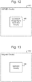
- FIG 12 is a schematic diagram of SAR-ADC circuitry 500 comprising the controllable voltage-signal generation circuitry 400.
- the SAR-ADC circuitry 500 could for example be the circuitry shown in Figure 5A , with the controllable voltage-signal generation circuitry 400 replacing the capacitors 370 and 371 and switches 360, and the node 403 could be connected to the comparator-input terminal 324.
- Figure 13 is a schematic diagram of integrated circuitry, such as an IC chip, comprising the SAR-ADC circuitry 500.
- the present invention extends to integrated circuitry and IC chips as mentioned above, circuit boards comprising such IC chips, and communication networks (for example, internet fiber-optic networks and wireless networks) and network equipment of such networks, comprising such circuit boards.
- communication networks for example, internet fiber-optic networks and wireless networks
- controllable voltage-signal generation circuitry 400 has been used to illustrate many examples herein however it is readily apparent that analogous considerations will apply in an n-bit CDAC.
- Controllable voltage-signal generation circuitry 400 has been illustrated as comprising three segments, each segment comprising three segment capacitors, however controllable voltage-signal generation circuitry 400 may comprise any number (but at least two) of segments and each segment may comprise any number of segment capacitors.
- the circuitry disclosed in for example Figure 6 may be referred to as a reconfigurable multi-segmented M x N (e.g. M segments, with N bits or segment capacitors per segment, where M and N are integers, M ⁇ 2, N ⁇ 1, and M and N are both 3 in the specific embodiment of Figure 6 ) CDAC with inherent gain & linearity calibration, suitable for use in a SAR ADC.
- M x N e.g. M segments, with N bits or segment capacitors per segment, where M and N are integers, M ⁇ 2, N ⁇ 1, and M and N are both 3 in the specific embodiment of Figure 6
- CDAC with inherent gain & linearity calibration
Landscapes
- Engineering & Computer Science (AREA)
- Theoretical Computer Science (AREA)
- Physics & Mathematics (AREA)
- Nonlinear Science (AREA)
- Power Engineering (AREA)
- Analogue/Digital Conversion (AREA)
Priority Applications (3)
| Application Number | Priority Date | Filing Date | Title |
|---|---|---|---|
| EP18214274.5A EP3672080B1 (de) | 2018-12-19 | 2018-12-19 | Spannungssignalerzeugung |
| US16/719,741 US10784887B2 (en) | 2018-12-19 | 2019-12-18 | Voltage-signal generation |
| CN201911319260.4A CN111342843B (zh) | 2018-12-19 | 2019-12-19 | 电压信号生成 |
Applications Claiming Priority (1)
| Application Number | Priority Date | Filing Date | Title |
|---|---|---|---|
| EP18214274.5A EP3672080B1 (de) | 2018-12-19 | 2018-12-19 | Spannungssignalerzeugung |
Publications (2)
| Publication Number | Publication Date |
|---|---|
| EP3672080A1 true EP3672080A1 (de) | 2020-06-24 |
| EP3672080B1 EP3672080B1 (de) | 2022-09-07 |
Family
ID=64746283
Family Applications (1)
| Application Number | Title | Priority Date | Filing Date |
|---|---|---|---|
| EP18214274.5A Active EP3672080B1 (de) | 2018-12-19 | 2018-12-19 | Spannungssignalerzeugung |
Country Status (3)
| Country | Link |
|---|---|
| US (1) | US10784887B2 (de) |
| EP (1) | EP3672080B1 (de) |
| CN (1) | CN111342843B (de) |
Families Citing this family (2)
| Publication number | Priority date | Publication date | Assignee | Title |
|---|---|---|---|---|
| US11522547B1 (en) * | 2021-05-31 | 2022-12-06 | Ceremorphic, Inc. | Bias unit element with binary weighted charge transfer capacitors |
| EP4236054A1 (de) * | 2022-02-23 | 2023-08-30 | Goodrich Control Systems | Steuergerät für einen leistungswandler |
Citations (3)
| Publication number | Priority date | Publication date | Assignee | Title |
|---|---|---|---|---|
| US5638072A (en) * | 1994-12-07 | 1997-06-10 | Sipex Corporation | Multiple channel analog to digital converter |
| EP2211468A1 (de) | 2009-01-26 | 2010-07-28 | Fujitsu Semiconductor Limited | Abtastung |
| CN101977058B (zh) * | 2010-10-28 | 2013-04-03 | 电子科技大学 | 带数字校正的逐次逼近模数转换器及其处理方法 |
Family Cites Families (10)
| Publication number | Priority date | Publication date | Assignee | Title |
|---|---|---|---|---|
| US4129863A (en) * | 1977-10-03 | 1978-12-12 | Regents Of The University Of California | Weighted capacitor analog/digital converting apparatus and method |
| US5581252A (en) * | 1994-10-13 | 1996-12-03 | Linear Technology Corporation | Analog-to-digital conversion using comparator coupled capacitor digital-to-analog converters |
| US7876254B2 (en) * | 2008-09-30 | 2011-01-25 | Freescale Semiconductor, Inc. | Data conversion circuitry having successive approximation circuitry and method therefor |
| DE102009010155B4 (de) | 2009-02-23 | 2013-02-07 | Texas Instruments Deutschland Gmbh | Digitales Trimmen von (SAR-)ADCs |
| US8031099B2 (en) * | 2009-12-23 | 2011-10-04 | Integrated Device Technology, Inc. | Analog/digital or digital/analog conversion system having improved linearity |
| US8446304B2 (en) | 2010-06-30 | 2013-05-21 | University Of Limerick | Digital background calibration system and method for successive approximation (SAR) analogue to digital converter |
| KR101716782B1 (ko) | 2010-09-30 | 2017-03-16 | 삼성전자 주식회사 | 디지털-아날로그 변환 회로 및 이를 포함하는 아날로그-디지털 변환기 |
| DE102011110115B4 (de) * | 2011-08-15 | 2015-02-26 | Texas Instruments Deutschland Gmbh | Vorrichtung und Verfahren zum Messen der DNL eines SAR ADC |
| WO2013099114A1 (ja) * | 2011-12-28 | 2013-07-04 | パナソニック株式会社 | 逐次比較型ad変換器およびノイズ生成器 |
| US8766833B1 (en) * | 2013-03-06 | 2014-07-01 | Infineon Technologies Austria Ag | System and method for calibrating a circuit |
-
2018
- 2018-12-19 EP EP18214274.5A patent/EP3672080B1/de active Active
-
2019
- 2019-12-18 US US16/719,741 patent/US10784887B2/en active Active
- 2019-12-19 CN CN201911319260.4A patent/CN111342843B/zh active Active
Patent Citations (3)
| Publication number | Priority date | Publication date | Assignee | Title |
|---|---|---|---|---|
| US5638072A (en) * | 1994-12-07 | 1997-06-10 | Sipex Corporation | Multiple channel analog to digital converter |
| EP2211468A1 (de) | 2009-01-26 | 2010-07-28 | Fujitsu Semiconductor Limited | Abtastung |
| CN101977058B (zh) * | 2010-10-28 | 2013-04-03 | 电子科技大学 | 带数字校正的逐次逼近模数转换器及其处理方法 |
Non-Patent Citations (1)
| Title |
|---|
| YAN ZHU ET AL: "A voltage feedback charge compensation technique for split DAC architecture in SAR ADCs", IEEE INTERNATIONAL SYMPOSIUM ON CIRCUITS AND SYSTEMS. ISCAS 2010 - 30 MAY-2 JUNE 2010 - PARIS, FRANCE, IEEE, US, 30 May 2010 (2010-05-30), pages 4061 - 4064, XP031724866, ISBN: 978-1-4244-5308-5 * |
Also Published As
| Publication number | Publication date |
|---|---|
| CN111342843B (zh) | 2023-06-27 |
| US10784887B2 (en) | 2020-09-22 |
| US20200204190A1 (en) | 2020-06-25 |
| EP3672080B1 (de) | 2022-09-07 |
| CN111342843A (zh) | 2020-06-26 |
Similar Documents
| Publication | Publication Date | Title |
|---|---|---|
| EP3514965B1 (de) | Analog-digital-wandlerschaltung | |
| EP2624458B1 (de) | Analog-Digital-Wandler mit Register zur schrittweisen Annäherung | |
| US8451151B2 (en) | Successive approximation analog to digital converter with capacitor mismatch calibration and method thereof | |
| US10637495B2 (en) | SAR ADCs with dedicated reference capacitor for each bit capacitor | |
| EP3537609B1 (de) | Verfahren zum anwenden von überlagerter schwingung und analog-digital-wandler gemäss dem verfahren | |
| US9912341B2 (en) | Data conversion with redundant split-capacitor arrangement | |
| US7286075B2 (en) | Analog to digital converter with dither | |
| US8310388B2 (en) | Subrange analog-to-digital converter and method thereof | |
| US5621409A (en) | Analog-to-digital conversion with multiple charge balance conversions | |
| US10581443B2 (en) | Method and apparatus for offset correction in SAR ADC with reduced capacitor array DAC | |
| US20130076546A1 (en) | Charge compensation calibration for high resolution data converter | |
| US20180205390A1 (en) | Gain calibration for adc with external reference | |
| US20100156689A1 (en) | A-d convert apparatus, d-a convert apparatus and adjustment method | |
| US9300312B2 (en) | Analog-digital converter | |
| KR20180041026A (ko) | Sar-adc 커패시터 어레이 장치 | |
| US10784887B2 (en) | Voltage-signal generation | |
| US10897261B1 (en) | Analog-to-digital converter with a supplementary digital-to-analog converter for offset and gain error measurements | |
| US12126355B2 (en) | Linearity and/or gain in mixed-signal circuitry | |
| US20230261663A1 (en) | Analog-to-digital converter circuit and semiconductor integrated circuit | |
| JP2026037854A (ja) | Ad変換回路 | |
| KR100336781B1 (ko) | 아날로그/디지털 변환기 | |
| JP2025017765A (ja) | 容量性d/aコンバータおよびa/dコンバータ | |
| Lee et al. | A 0.7 V 810µW 10b 30MS/s comparator-based two-step pipelined ADC | |
| Keskin | A Background Mismatch Calibration For Capacitive Digitial-To-Analog Converters RTERS |
Legal Events
| Date | Code | Title | Description |
|---|---|---|---|
| PUAI | Public reference made under article 153(3) epc to a published international application that has entered the european phase |
Free format text: ORIGINAL CODE: 0009012 |
|
| STAA | Information on the status of an ep patent application or granted ep patent |
Free format text: STATUS: THE APPLICATION HAS BEEN PUBLISHED |
|
| AK | Designated contracting states |
Kind code of ref document: A1 Designated state(s): AL AT BE BG CH CY CZ DE DK EE ES FI FR GB GR HR HU IE IS IT LI LT LU LV MC MK MT NL NO PL PT RO RS SE SI SK SM TR |
|
| AX | Request for extension of the european patent |
Extension state: BA ME |
|
| STAA | Information on the status of an ep patent application or granted ep patent |
Free format text: STATUS: REQUEST FOR EXAMINATION WAS MADE |
|
| 17P | Request for examination filed |
Effective date: 20201222 |
|
| RBV | Designated contracting states (corrected) |
Designated state(s): AL AT BE BG CH CY CZ DE DK EE ES FI FR GB GR HR HU IE IS IT LI LT LU LV MC MK MT NL NO PL PT RO RS SE SI SK SM TR |
|
| GRAP | Despatch of communication of intention to grant a patent |
Free format text: ORIGINAL CODE: EPIDOSNIGR1 |
|
| STAA | Information on the status of an ep patent application or granted ep patent |
Free format text: STATUS: GRANT OF PATENT IS INTENDED |
|
| INTG | Intention to grant announced |
Effective date: 20211216 |
|
| GRAJ | Information related to disapproval of communication of intention to grant by the applicant or resumption of examination proceedings by the epo deleted |
Free format text: ORIGINAL CODE: EPIDOSDIGR1 |
|
| STAA | Information on the status of an ep patent application or granted ep patent |
Free format text: STATUS: REQUEST FOR EXAMINATION WAS MADE |
|
| INTC | Intention to grant announced (deleted) | ||
| GRAP | Despatch of communication of intention to grant a patent |
Free format text: ORIGINAL CODE: EPIDOSNIGR1 |
|
| STAA | Information on the status of an ep patent application or granted ep patent |
Free format text: STATUS: GRANT OF PATENT IS INTENDED |
|
| GRAJ | Information related to disapproval of communication of intention to grant by the applicant or resumption of examination proceedings by the epo deleted |
Free format text: ORIGINAL CODE: EPIDOSDIGR1 |
|
| STAA | Information on the status of an ep patent application or granted ep patent |
Free format text: STATUS: REQUEST FOR EXAMINATION WAS MADE |
|
| INTG | Intention to grant announced |
Effective date: 20220512 |
|
| GRAP | Despatch of communication of intention to grant a patent |
Free format text: ORIGINAL CODE: EPIDOSNIGR1 |
|
| STAA | Information on the status of an ep patent application or granted ep patent |
Free format text: STATUS: GRANT OF PATENT IS INTENDED |
|
| INTC | Intention to grant announced (deleted) | ||
| INTG | Intention to grant announced |
Effective date: 20220621 |
|
| GRAS | Grant fee paid |
Free format text: ORIGINAL CODE: EPIDOSNIGR3 |
|
| GRAA | (expected) grant |
Free format text: ORIGINAL CODE: 0009210 |
|
| STAA | Information on the status of an ep patent application or granted ep patent |
Free format text: STATUS: THE PATENT HAS BEEN GRANTED |
|
| AK | Designated contracting states |
Kind code of ref document: B1 Designated state(s): AL AT BE BG CH CY CZ DE DK EE ES FI FR GB GR HR HU IE IS IT LI LT LU LV MC MK MT NL NO PL PT RO RS SE SI SK SM TR |
|
| REG | Reference to a national code |
Ref country code: GB Ref legal event code: FG4D |
|
| REG | Reference to a national code |
Ref country code: CH Ref legal event code: EP Ref country code: AT Ref legal event code: REF Ref document number: 1517897 Country of ref document: AT Kind code of ref document: T Effective date: 20220915 |
|
| REG | Reference to a national code |
Ref country code: DE Ref legal event code: R096 Ref document number: 602018040282 Country of ref document: DE |
|
| REG | Reference to a national code |
Ref country code: IE Ref legal event code: FG4D |
|
| REG | Reference to a national code |
Ref country code: LT Ref legal event code: MG9D |
|
| REG | Reference to a national code |
Ref country code: NL Ref legal event code: MP Effective date: 20220907 |
|
| PG25 | Lapsed in a contracting state [announced via postgrant information from national office to epo] |
Ref country code: SE Free format text: LAPSE BECAUSE OF FAILURE TO SUBMIT A TRANSLATION OF THE DESCRIPTION OR TO PAY THE FEE WITHIN THE PRESCRIBED TIME-LIMIT Effective date: 20220907 Ref country code: RS Free format text: LAPSE BECAUSE OF FAILURE TO SUBMIT A TRANSLATION OF THE DESCRIPTION OR TO PAY THE FEE WITHIN THE PRESCRIBED TIME-LIMIT Effective date: 20220907 Ref country code: NO Free format text: LAPSE BECAUSE OF FAILURE TO SUBMIT A TRANSLATION OF THE DESCRIPTION OR TO PAY THE FEE WITHIN THE PRESCRIBED TIME-LIMIT Effective date: 20221207 Ref country code: LV Free format text: LAPSE BECAUSE OF FAILURE TO SUBMIT A TRANSLATION OF THE DESCRIPTION OR TO PAY THE FEE WITHIN THE PRESCRIBED TIME-LIMIT Effective date: 20220907 Ref country code: LT Free format text: LAPSE BECAUSE OF FAILURE TO SUBMIT A TRANSLATION OF THE DESCRIPTION OR TO PAY THE FEE WITHIN THE PRESCRIBED TIME-LIMIT Effective date: 20220907 Ref country code: FI Free format text: LAPSE BECAUSE OF FAILURE TO SUBMIT A TRANSLATION OF THE DESCRIPTION OR TO PAY THE FEE WITHIN THE PRESCRIBED TIME-LIMIT Effective date: 20220907 |
|
| REG | Reference to a national code |
Ref country code: AT Ref legal event code: MK05 Ref document number: 1517897 Country of ref document: AT Kind code of ref document: T Effective date: 20220907 |
|
| PG25 | Lapsed in a contracting state [announced via postgrant information from national office to epo] |
Ref country code: HR Free format text: LAPSE BECAUSE OF FAILURE TO SUBMIT A TRANSLATION OF THE DESCRIPTION OR TO PAY THE FEE WITHIN THE PRESCRIBED TIME-LIMIT Effective date: 20220907 Ref country code: GR Free format text: LAPSE BECAUSE OF FAILURE TO SUBMIT A TRANSLATION OF THE DESCRIPTION OR TO PAY THE FEE WITHIN THE PRESCRIBED TIME-LIMIT Effective date: 20221208 |
|
| PG25 | Lapsed in a contracting state [announced via postgrant information from national office to epo] |
Ref country code: SM Free format text: LAPSE BECAUSE OF FAILURE TO SUBMIT A TRANSLATION OF THE DESCRIPTION OR TO PAY THE FEE WITHIN THE PRESCRIBED TIME-LIMIT Effective date: 20220907 Ref country code: RO Free format text: LAPSE BECAUSE OF FAILURE TO SUBMIT A TRANSLATION OF THE DESCRIPTION OR TO PAY THE FEE WITHIN THE PRESCRIBED TIME-LIMIT Effective date: 20220907 Ref country code: PT Free format text: LAPSE BECAUSE OF FAILURE TO SUBMIT A TRANSLATION OF THE DESCRIPTION OR TO PAY THE FEE WITHIN THE PRESCRIBED TIME-LIMIT Effective date: 20230109 Ref country code: ES Free format text: LAPSE BECAUSE OF FAILURE TO SUBMIT A TRANSLATION OF THE DESCRIPTION OR TO PAY THE FEE WITHIN THE PRESCRIBED TIME-LIMIT Effective date: 20220907 Ref country code: CZ Free format text: LAPSE BECAUSE OF FAILURE TO SUBMIT A TRANSLATION OF THE DESCRIPTION OR TO PAY THE FEE WITHIN THE PRESCRIBED TIME-LIMIT Effective date: 20220907 Ref country code: AT Free format text: LAPSE BECAUSE OF FAILURE TO SUBMIT A TRANSLATION OF THE DESCRIPTION OR TO PAY THE FEE WITHIN THE PRESCRIBED TIME-LIMIT Effective date: 20220907 |
|
| PG25 | Lapsed in a contracting state [announced via postgrant information from national office to epo] |
Ref country code: SK Free format text: LAPSE BECAUSE OF FAILURE TO SUBMIT A TRANSLATION OF THE DESCRIPTION OR TO PAY THE FEE WITHIN THE PRESCRIBED TIME-LIMIT Effective date: 20220907 Ref country code: PL Free format text: LAPSE BECAUSE OF FAILURE TO SUBMIT A TRANSLATION OF THE DESCRIPTION OR TO PAY THE FEE WITHIN THE PRESCRIBED TIME-LIMIT Effective date: 20220907 Ref country code: IS Free format text: LAPSE BECAUSE OF FAILURE TO SUBMIT A TRANSLATION OF THE DESCRIPTION OR TO PAY THE FEE WITHIN THE PRESCRIBED TIME-LIMIT Effective date: 20230107 Ref country code: EE Free format text: LAPSE BECAUSE OF FAILURE TO SUBMIT A TRANSLATION OF THE DESCRIPTION OR TO PAY THE FEE WITHIN THE PRESCRIBED TIME-LIMIT Effective date: 20220907 |
|
| REG | Reference to a national code |
Ref country code: DE Ref legal event code: R097 Ref document number: 602018040282 Country of ref document: DE |
|
| PG25 | Lapsed in a contracting state [announced via postgrant information from national office to epo] |
Ref country code: NL Free format text: LAPSE BECAUSE OF FAILURE TO SUBMIT A TRANSLATION OF THE DESCRIPTION OR TO PAY THE FEE WITHIN THE PRESCRIBED TIME-LIMIT Effective date: 20220907 Ref country code: AL Free format text: LAPSE BECAUSE OF FAILURE TO SUBMIT A TRANSLATION OF THE DESCRIPTION OR TO PAY THE FEE WITHIN THE PRESCRIBED TIME-LIMIT Effective date: 20220907 |
|
| PLBE | No opposition filed within time limit |
Free format text: ORIGINAL CODE: 0009261 |
|
| STAA | Information on the status of an ep patent application or granted ep patent |
Free format text: STATUS: NO OPPOSITION FILED WITHIN TIME LIMIT |
|
| PG25 | Lapsed in a contracting state [announced via postgrant information from national office to epo] |
Ref country code: DK Free format text: LAPSE BECAUSE OF FAILURE TO SUBMIT A TRANSLATION OF THE DESCRIPTION OR TO PAY THE FEE WITHIN THE PRESCRIBED TIME-LIMIT Effective date: 20220907 |
|
| REG | Reference to a national code |
Ref country code: CH Ref legal event code: PL |
|
| 26N | No opposition filed |
Effective date: 20230608 |
|
| GBPC | Gb: european patent ceased through non-payment of renewal fee |
Effective date: 20221219 |
|
| REG | Reference to a national code |
Ref country code: BE Ref legal event code: MM Effective date: 20221231 |
|
| PG25 | Lapsed in a contracting state [announced via postgrant information from national office to epo] |
Ref country code: SI Free format text: LAPSE BECAUSE OF FAILURE TO SUBMIT A TRANSLATION OF THE DESCRIPTION OR TO PAY THE FEE WITHIN THE PRESCRIBED TIME-LIMIT Effective date: 20220907 Ref country code: LU Free format text: LAPSE BECAUSE OF NON-PAYMENT OF DUE FEES Effective date: 20221219 |
|
| PG25 | Lapsed in a contracting state [announced via postgrant information from national office to epo] |
Ref country code: LI Free format text: LAPSE BECAUSE OF NON-PAYMENT OF DUE FEES Effective date: 20221231 Ref country code: IE Free format text: LAPSE BECAUSE OF NON-PAYMENT OF DUE FEES Effective date: 20221219 Ref country code: GB Free format text: LAPSE BECAUSE OF NON-PAYMENT OF DUE FEES Effective date: 20221219 Ref country code: CH Free format text: LAPSE BECAUSE OF NON-PAYMENT OF DUE FEES Effective date: 20221231 |
|
| PG25 | Lapsed in a contracting state [announced via postgrant information from national office to epo] |
Ref country code: FR Free format text: LAPSE BECAUSE OF NON-PAYMENT OF DUE FEES Effective date: 20221231 Ref country code: BE Free format text: LAPSE BECAUSE OF NON-PAYMENT OF DUE FEES Effective date: 20221231 |
|
| PG25 | Lapsed in a contracting state [announced via postgrant information from national office to epo] |
Ref country code: HU Free format text: LAPSE BECAUSE OF FAILURE TO SUBMIT A TRANSLATION OF THE DESCRIPTION OR TO PAY THE FEE WITHIN THE PRESCRIBED TIME-LIMIT; INVALID AB INITIO Effective date: 20181219 |
|
| PG25 | Lapsed in a contracting state [announced via postgrant information from national office to epo] |
Ref country code: CY Free format text: LAPSE BECAUSE OF FAILURE TO SUBMIT A TRANSLATION OF THE DESCRIPTION OR TO PAY THE FEE WITHIN THE PRESCRIBED TIME-LIMIT Effective date: 20220907 |
|
| PG25 | Lapsed in a contracting state [announced via postgrant information from national office to epo] |
Ref country code: MK Free format text: LAPSE BECAUSE OF FAILURE TO SUBMIT A TRANSLATION OF THE DESCRIPTION OR TO PAY THE FEE WITHIN THE PRESCRIBED TIME-LIMIT Effective date: 20220907 Ref country code: IT Free format text: LAPSE BECAUSE OF FAILURE TO SUBMIT A TRANSLATION OF THE DESCRIPTION OR TO PAY THE FEE WITHIN THE PRESCRIBED TIME-LIMIT Effective date: 20220907 |
|
| PG25 | Lapsed in a contracting state [announced via postgrant information from national office to epo] |
Ref country code: MC Free format text: LAPSE BECAUSE OF FAILURE TO SUBMIT A TRANSLATION OF THE DESCRIPTION OR TO PAY THE FEE WITHIN THE PRESCRIBED TIME-LIMIT Effective date: 20220907 |
|
| PG25 | Lapsed in a contracting state [announced via postgrant information from national office to epo] |
Ref country code: TR Free format text: LAPSE BECAUSE OF FAILURE TO SUBMIT A TRANSLATION OF THE DESCRIPTION OR TO PAY THE FEE WITHIN THE PRESCRIBED TIME-LIMIT Effective date: 20220907 Ref country code: MC Free format text: LAPSE BECAUSE OF FAILURE TO SUBMIT A TRANSLATION OF THE DESCRIPTION OR TO PAY THE FEE WITHIN THE PRESCRIBED TIME-LIMIT Effective date: 20220907 |
|
| PG25 | Lapsed in a contracting state [announced via postgrant information from national office to epo] |
Ref country code: BG Free format text: LAPSE BECAUSE OF FAILURE TO SUBMIT A TRANSLATION OF THE DESCRIPTION OR TO PAY THE FEE WITHIN THE PRESCRIBED TIME-LIMIT Effective date: 20220907 |
|
| PG25 | Lapsed in a contracting state [announced via postgrant information from national office to epo] |
Ref country code: MT Free format text: LAPSE BECAUSE OF FAILURE TO SUBMIT A TRANSLATION OF THE DESCRIPTION OR TO PAY THE FEE WITHIN THE PRESCRIBED TIME-LIMIT Effective date: 20220907 |
|
| PGFP | Annual fee paid to national office [announced via postgrant information from national office to epo] |
Ref country code: DE Payment date: 20251211 Year of fee payment: 8 |