EP3671956B1 - Doppelfrequenz-patchantennen - Google Patents
Doppelfrequenz-patchantennen Download PDFInfo
- Publication number
- EP3671956B1 EP3671956B1 EP20157422.5A EP20157422A EP3671956B1 EP 3671956 B1 EP3671956 B1 EP 3671956B1 EP 20157422 A EP20157422 A EP 20157422A EP 3671956 B1 EP3671956 B1 EP 3671956B1
- Authority
- EP
- European Patent Office
- Prior art keywords
- conductive element
- dual
- circuitry
- dielectric material
- conductive
- Prior art date
- Legal status (The legal status is an assumption and is not a legal conclusion. Google has not performed a legal analysis and makes no representation as to the accuracy of the status listed.)
- Active
Links
Images





Classifications
-
- H—ELECTRICITY
- H01—ELECTRIC ELEMENTS
- H01Q—ANTENNAS, i.e. RADIO AERIALS
- H01Q9/00—Electrically-short antennas having dimensions not more than twice the operating wavelength and consisting of conductive active radiating elements
- H01Q9/04—Resonant antennas
- H01Q9/0407—Substantially flat resonant element parallel to ground plane, e.g. patch antenna
-
- G—PHYSICS
- G01—MEASURING; TESTING
- G01S—RADIO DIRECTION-FINDING; RADIO NAVIGATION; DETERMINING DISTANCE OR VELOCITY BY USE OF RADIO WAVES; LOCATING OR PRESENCE-DETECTING BY USE OF THE REFLECTION OR RERADIATION OF RADIO WAVES; ANALOGOUS ARRANGEMENTS USING OTHER WAVES
- G01S19/00—Satellite radio beacon positioning systems; Determining position, velocity or attitude using signals transmitted by such systems
- G01S19/01—Satellite radio beacon positioning systems transmitting time-stamped messages, e.g. GPS [Global Positioning System], GLONASS [Global Orbiting Navigation Satellite System] or GALILEO
- G01S19/13—Receivers
- G01S19/32—Multimode operation in a single same satellite system, e.g. GPS L1/L2
-
- G—PHYSICS
- G01—MEASURING; TESTING
- G01S—RADIO DIRECTION-FINDING; RADIO NAVIGATION; DETERMINING DISTANCE OR VELOCITY BY USE OF RADIO WAVES; LOCATING OR PRESENCE-DETECTING BY USE OF THE REFLECTION OR RERADIATION OF RADIO WAVES; ANALOGOUS ARRANGEMENTS USING OTHER WAVES
- G01S19/00—Satellite radio beacon positioning systems; Determining position, velocity or attitude using signals transmitted by such systems
- G01S19/01—Satellite radio beacon positioning systems transmitting time-stamped messages, e.g. GPS [Global Positioning System], GLONASS [Global Orbiting Navigation Satellite System] or GALILEO
- G01S19/13—Receivers
- G01S19/35—Constructional details or hardware or software details of the signal processing chain
- G01S19/36—Constructional details or hardware or software details of the signal processing chain relating to the receiver frond end
-
- H—ELECTRICITY
- H01—ELECTRIC ELEMENTS
- H01Q—ANTENNAS, i.e. RADIO AERIALS
- H01Q1/00—Details of, or arrangements associated with, antennas
- H01Q1/48—Earthing means; Earth screens; Counterpoises
-
- H—ELECTRICITY
- H01—ELECTRIC ELEMENTS
- H01Q—ANTENNAS, i.e. RADIO AERIALS
- H01Q1/00—Details of, or arrangements associated with, antennas
- H01Q1/52—Means for reducing coupling between antennas; Means for reducing coupling between an antenna and another structure
- H01Q1/521—Means for reducing coupling between antennas; Means for reducing coupling between an antenna and another structure reducing the coupling between adjacent antennas
-
- H—ELECTRICITY
- H01—ELECTRIC ELEMENTS
- H01Q—ANTENNAS, i.e. RADIO AERIALS
- H01Q5/00—Arrangements for simultaneous operation of antennas on two or more different wavebands, e.g. dual-band or multi-band arrangements
- H01Q5/30—Arrangements for providing operation on different wavebands
- H01Q5/307—Individual or coupled radiating elements, each element being fed in an unspecified way
- H01Q5/314—Individual or coupled radiating elements, each element being fed in an unspecified way using frequency dependent circuits or components, e.g. trap circuits or capacitors
- H01Q5/335—Individual or coupled radiating elements, each element being fed in an unspecified way using frequency dependent circuits or components, e.g. trap circuits or capacitors at the feed, e.g. for impedance matching
-
- H—ELECTRICITY
- H01—ELECTRIC ELEMENTS
- H01Q—ANTENNAS, i.e. RADIO AERIALS
- H01Q5/00—Arrangements for simultaneous operation of antennas on two or more different wavebands, e.g. dual-band or multi-band arrangements
- H01Q5/30—Arrangements for providing operation on different wavebands
- H01Q5/378—Combination of fed elements with parasitic elements
-
- H—ELECTRICITY
- H01—ELECTRIC ELEMENTS
- H01Q—ANTENNAS, i.e. RADIO AERIALS
- H01Q5/00—Arrangements for simultaneous operation of antennas on two or more different wavebands, e.g. dual-band or multi-band arrangements
- H01Q5/40—Imbricated or interleaved structures; Combined or electromagnetically coupled arrangements, e.g. comprising two or more non-connected fed radiating elements
-
- H—ELECTRICITY
- H01—ELECTRIC ELEMENTS
- H01Q—ANTENNAS, i.e. RADIO AERIALS
- H01Q9/00—Electrically-short antennas having dimensions not more than twice the operating wavelength and consisting of conductive active radiating elements
- H01Q9/04—Resonant antennas
- H01Q9/0407—Substantially flat resonant element parallel to ground plane, e.g. patch antenna
- H01Q9/0414—Substantially flat resonant element parallel to ground plane, e.g. patch antenna in a stacked or folded configuration
-
- H—ELECTRICITY
- H01—ELECTRIC ELEMENTS
- H01Q—ANTENNAS, i.e. RADIO AERIALS
- H01Q9/00—Electrically-short antennas having dimensions not more than twice the operating wavelength and consisting of conductive active radiating elements
- H01Q9/04—Resonant antennas
- H01Q9/0407—Substantially flat resonant element parallel to ground plane, e.g. patch antenna
- H01Q9/045—Substantially flat resonant element parallel to ground plane, e.g. patch antenna with particular feeding means
Definitions
- Embodiments described herein relate generally to dual-frequency patch antennas and methods for forming parts of dual-frequency patch antennas using printed circuit board assembly (PCBA) processes.
- PCBA printed circuit board assembly
- Patch (or microstrip) antennas typcially include a flat metal sheet mounted over a larger metal ground plane.
- the flat metal sheet usually has a rectangular shape, and the metal layers are generally separated using a dielectric spacer.
- the flat metal sheet has a length of approximatley ⁇ /2, and width can be optimized to provide a desired imput impedance.
- Patch antennas can be configured to provide linear or circular polarization.
- Dual-frequency patch antennas typically include two flat metal sheets mounted over a larger ground plane. Dual-frequency patch antennas exhibit a dual-resonant behavior in a single radiating structure, and they are often used in applications where increased bandwidth is needed or for operating at two separate sub-bands.
- Global navigation satellite system (GNSS) receivers often use right-handed circularly polarized (RHCP) dual-frequency patch antennas to receive GNSS signals at different frequencies (e.g., L1, L2, L2C, L3, L4, L5, and other GNSS frequencies).
- Patch antennas are popular because of their simple design, low profile, light weight, and low cost. Improved designs are constantly sought to improve performance and further reduce cost. Prior art antennas are disclosed, for example, in CN 102 496 783 , CN 101 051 707 , CN 103 022 731 , and CN 103 022 663 .
- Embodiments described herein provide dual-frequency patch antennas that may be smaller, lighter, and/or lower cost than conventional dual-frequency patch antennas.
- a dual-frequency patch antenna as set out in claim 1 is provided.
- the dependent claims relate to preferred embodiments.
- the routing and placement layer with circuitry is formed below the ground plane.
- the routing and placement layer is separated from the ground plane by a bottom dielectric layer (one of the three dielectric layers). Forming the circuitry below the ground plane can also reduce size, weight, and/or lower cost compared to conventional structures that form the circuitry adjacent to the ground plane or on a separate board.
- the circuitry layer may be coupled to an output that is configured to provide digitized baseband signals from the circuitry to a digital cable.
- the digital cable may provide the digitized baseband signals to a processing device, such as a cell phone or a tablet computer, where pseudorange and carrier phase measurements are performed.
- Embodiments described herein provide dual-frequency patch antennas and methods for forming parts of dual-frequency patch antennas using PCBA processes.
- a dual-frequency patch antenna that includes circuitry for frequency selection, down conversion, and/or digitization may be formed using a vertical stack of dielectric layers, condutcive layers, and circuitry.
- One or more of the dielectric layers and conductive layers, as well as the circuitry, may be formed using PCBA processes.
- the circuitry may include elements to filter, amplify, downconvert, and digitize GNSS signals, but may not include elements to perform pseudorange and carrier phase measurements.
- the pseudorange and carrier phase measurements, as well as the application of any corrections may be performed by a communication device that is configured with a software-defined GNSS receiver (soft GNSS receiver).
- the dual-frequency patch antenna may be removably coupled with the communication device.
- the communication device is not limited and may be any device such as a cell phone, a tablet computer, or the like with computing capabilities for processing digitized baseband signals at typical sampling rates.
- the communication device may be configured in accordance with known techniques to perform conventional GNSS measurements and determine position fixes associated with the dual-frequency patch antenna.
- the soft GNSS receiver may run as software on one or more processors that are part of the communication device.
- a digital cable such as a USB cable, an Ethernet cable, or the like, may be used to provide digitized baseband signals from the circuitry of the patch antenna to the soft GNSS receiver of the communication device.
- FIG. 1A is a simplified perspective view of a dual-frequency patch antenna in accordance with an example.
- the patch antenna includes a first conductive clement 102 configured to receive GNSS signals at a first frequency band and a second conductive clement 106 configured to receive GNSS signals at a second frequency band.
- a first dielectric material 104 is coupled to a backside of the first conductive clement 102, and the second conductive element 106 is coupled to a backside of the first dielectric material 104.
- a second dielectric material 108 is coupled to a backside of the second conductive element 106.
- the dielectric materials 104, 108 may be coupled to the conductive elements 102, 106 using known PCBA processes and adhesives.
- FIG. 1B is a simplified plan view of the dual-frequency patch antenna shown in FIG. 1A .
- This figure shows the conductive elements 102, 106 and the dielectric materials 104, 108.
- the second conductive element 106 has a topside with an area that is larger than a topside of the first conductive element 102, but in other embodiments, the second conductive clement 106 may have a topside with an area that is approximately the same size as the topside of the first conductive element 102.
- the patch antenna also includes a ground plane 110 coupled to a backside of the second dielectric material 108, a third dielectric material 112 coupled to a backside of the ground plane 110, and a routing and placement layer 114 with circuitry 121 coupled to a backside of the third dielectric layer coupled to a backside of the third dielectric layer.
- the ground plane 110 typically has a topside with an area at least as large or larger than a topside of the second conductive element 106.
- the second dielectric material 108 has a topside with an area that is at least as large as the topside of the ground plane 110.
- the dielectric materials 104, 108, 112 are not limited and may include any solid or laminate dielectric materials such as ceramics, printed circuit board (PCB) cores, pre-preg layers, or the like. Thickness and dielectric constant of the dielectric materials 104, 108 may be determined in accordance with known techniques based on desired operating conditions of the patch antenna (e.g., radiation patterns, coupling between patches, etc.). The dielectric materials 104, 108, 112 may each have the same or different thicknesses and dielectric constants. In some embodiments, the second dielectric material 108 has a topside with an area that is larger than a topside of the first dielectric material 104.
- the third dielectric material 112 may include one or more conductive routing layers each disposed between adjacent dielectric layers (e.g., pre-preg layers). Each of the conductive routing layers may be electrically coupled to other conductive routing layers, the routing and placement layer 114, the circuitry 121, and/or one or more feeds.
- the routing layers may include vias and/or conductive traces that provide electrical coupling between the circuitry 121 (or components of the circuitry 121) and the first conductive element 102 and/or the second conductive element 106. The electrical coupling is provided via the routing and placement layer 114 and one or more feeds (e.g., feeds 115, 116, 117, 118, 119 - described more fully below).
- the conductive elements 102, 106 and the ground plane 110 are not limited and may include any conductive material such as a metal, alloy, or the like.
- the conductive elements 102, 106 and the ground plane 110 may be thin copper sheets that arc formed in a desired shape using known PCBA processes and etching techniques.
- the conductive elements 102, 106 and the ground plane 110 are typically rectangular shaped, but may be other shapes including circular.
- the size and shape of the conductive elements 102, 106 are determined in accordance with known techniques based on desired operating conditions of the patch antenna (e.g., operating frequencies, bandwidths, input impedances, etc.).
- the first conductive element 102 is configured to receive L1 GNSS signals and the second conductive element 106 is configured to receive either L2 GNSS signals (where the L2 GNSS signals may be either L2 or L2C GNSS signals), L5 GNSS signals, or any other GNSS signals (e.g., L3 or L4 GNSS signals).
- the conductive elements 102, 106 are not limited, however, and each conductive clement may be configured to receive signals at any particular GNSS frequency.
- the second conductive element 106 may be configured to receive L1 GNSS signals
- the first conductive element 102 may be configured to receive signals at another GNSS frequency.
- FIGS. 1C-1E are simplified cross-sectional views along line A-A in FIG. 1B and show different examples of dual-frequency patch antennas.
- Each of the examples shown in FIGS. 1C-1E include the conductive elements 102, 106 and the dielectric materials 104, 108 as shown in FIGS. 1A-1B , as well as the ground plane 110, the third dielectric material 112, the routing and placement layer 114, and the circuitry 121 described above.
- the circuitry 121 may include conventional electronic components for providing at least frequency selection of GNSS signals received by the conductive elements 102, 106.
- the circuitry 121 may also include conventional electronic components for providing down conversion of the GNSS signals, and in other examples, the circuitry 121 may also include conventional electronic components for providing down conversion and digitization of the GNSS signals.
- the electronic components may be mounted on a circuit board in accordance with known techniques. Although not specifically shown in the figures, the electronic components may include one or more known components such as filters, low noise amplifiers (LNAs), down converters, analog to digital (A/D) converters, processors, and/or the like.
- the one or more processors may be configured to package the GNSS signals for output from the circuitry 121 at output 120.
- the routing and placement layer 114 may include one or more layers of conductive traces that provide electrical coupling between the components of the circuitry 121 and the conductive elements 102, 106.
- the routing and placement layer 114 shown in these examples is approximately the same size (in cross section) as the ground plane 110, a surface area of the routing and placement layer 114 is not limited and may be either smaller, the same size, or larger than that of the ground plane 110.
- the output 120 may provide an interface between the circuitry 121 and a soft GNSS receiver separate from the dual-frequency patch antenna. As described previously, the soft GNSS receiver may run as software on a separate communication device. The output 120 may provide the GNSS signals using known wireless techniques (e.g., Bluetooth) or via a digital cable 122 as shown in FIG. 1C .
- the digital cable may include a USB cable (e.g., USB 2.0 high speed, USB 3.0, etc.), an Ethernet cable, or the like, and may be used to provide the GNSS signals from the circuitry 121 of the patch antenna to the soft GNSS receiver of the communication device.
- each of the examples of dual-frequency patch antennas described herein may provide the GNSS signals from the circuitry either wirelessly or via a digital cable.
- the GNSS signals output from the circuitry 121 may be either frequency selected and amplified GNSS signals; frequency selected, amplified, and downconverted GNSS signals; or frequency selected, amplified, downconverted, and digitized GNSS signals (digitized baseband signals).
- the examples shown in FIGS. 1C-1E also include one or more feeds (feeds 115, 116, 117, 118, 119).
- the feeds are for electrically coupling the circuitry 121 to the first conductive clement 102 and/or the second conductive element 106 via the routing and placement layer 114.
- the example shown in FIG. 1C includes a first feed 115 coupling the circuitry 121 to the second conductive element 106 and a second feed 116 coupling the circuitry 121 to the first conductive element 102.
- the feeds 115, 116 provide energy from the conductive elements 102, 106 to the circuitry 121.
- the example shown in FIG. 1D includes a first feed 117 coupling the circuitry 121 to the second conductive element 106 and a second feed 118 coupling the circuitry 121 to the first conductive clement 102.
- the feeds 117, 118 terminate in the third dielectric material 112 and are coupled to the circuitry 121 by one or more routing layers (not shown).
- the example shown in FIG. 1E includes a single feed 119 coupling the circuitry 121 to the first conductive element 102. While the second conductive clement 106 is electrically isolated from the circuitry 121 in this example, the second conductive element is capacitively coupled to the first conductive element 102 (and hence capacitivcly coupled to the circuitry 121). In other examples, a single feed may be used in a similar manner to couple the circuitry 121 to the second conductive element 106 leaving the first conductive element 102 electrically isolated from, but capacitively coupled to, the circuitry 121. Polarization of the dual-frequency patch antenna may be determined in accordance with known techniques based on feed location on the conductive elements 102, 106.
- the feeds 115, 116, 117, 118, 119 are shown merely as examples of some of the feed configurations that may be used with embodiments of dual-frequency patch antennas described herein.
- the dual-frequency patch antennas described herein are not limited to these or any other feed configurations.
- one or both of the conductive elements may have dual feeds in some embodiments.
- many details associated with the feeds are not included in the figures.
- the feeds typically pass through a hole or aperture in the ground plane that provides isolation from the ground plane.
- the feeds that are coupled to the top conductive element (the first conductive clement 102) may pass through a hole or aperture in the bottom conductive element (the second conductive element 106) that provides isolation from the bottom conductive element.
- the feeds may be coupled with the conductive elements at different locations in accordance with known techniques based on desired polarization characteristics.
- the feeds may be coupled at various points (e.g., top or bottom) of the conductive elements and the routing and placement layer, and the feeds may extend horizontally before extending vertically through the dielectric layers or even wrap around the dielectric layers.
- FIGS. 1C-1E merely provide some of the general feed configurations that may be used with the dual-frequency patch antennas that are within the scope of this disclosure. And while all of the examples may include feeds, the feeds are not specifically shown in any of the other figures.
- FIGS. 2A-2C are simplified diagrams of a dual-frequency patch antenna in accordance with an example. These figures show a first conductive element 202, a first dielectric material 204, a second conductive element 206, and a second dielectric material 208.
- FIG. 2C which is a cross-sectional view along line B-B in FIG. 2B , also shows a ground plane 210, a third dielectric material 212, routing and placement layer 114, circuitry 221, and an output 220.
- Each of the layers and/or components may include features similar to those described above with regard to FIGS. 1A-1E . As can be seen from the dotted line in FIG. 2A , and in the cross section of FIG.
- the second conductive element 206 is approximately the same size as the first conductive element 202.
- the sizes of the first conductive element 202 and the second conductive element 206 may be determined in accordance with known techniques and may depend at least in part on dielectric constants of the dielectric materials 204, 206.
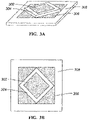
- FIGS. 3A-3B are simplified diagrams of a dual-frequency patch antenna in accordance with another embodiment.
- edges of a first conductive element 302 and a first dielectric material 304 are rotated relative to edges of a second conductive element 306 and a second dielectric material 308. Rotation can provide improved isolation between the conductive elements 302, 306 in some configurations and operating conditions.
- the first conductive element 302 and the first dielectric material 304 may be rotated by about 45° (or between about 30° and 60°). Also, the first conductive element 302 and the first dielectric material 304 may be larger than shown in FIGS.
- this embodiment also includes a ground plane, third dielectric material, routing and placement layer, circuitry, and preferably output similar to that shown in FIGS. 1C-1E and FIG. 2C .
- Each of the layers and/or components may include features similar to those described above with regard to FIGS. 1A-1E .
- FIGS. 4A-4C are simplified diagrams of a dual-frequency patch antenna in accordance with another example. These figures show a first conductive clement 402, a first dielectric material 404, a second conductive element 406, and a second dielectric material 408.
- FIG. 4C which is a cross-sectional view along line C-C in FIG. 4B , also shows a ground plane 410, a third dielectric material 412, routing and placement layer 414, circuitry 421, and an output 420.
- a first dielectric material 404 is approximately the same size as a second dielectric material 408. Also, as shown by the dotted line in FIGS.
- the first conductive element 402 is smaller than the second conductive clement 404 in this example, although as described with regard to other examples, the conductive elements 402, 406 may be approximately the same size.
- Each of the layers and/or components may include features similar to those described above with regard to FIGS. 1A-1E .
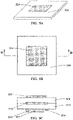
- FIGS. 5A-5C are simplified diagrams of a dual-frequency patch antenna in accordance with another example. These figures show a conductive clement 524 and a top dielectric material 504.
- FIG. 5C which is a cross-sectional view along line D-D in FIG. 5B , also shows a ground plane 510, a bottom dielectric material 512, routing and placement layer 514, circuitry 521, and an output 520.
- Each of the layers and/or components may include features similar to those described above with regard to FIGS. 1A-1E .
- the bottom dielectric material 512 may include one or more conductive routing layers each disposed between adjacent dielectric layers as described above with regard to the third dielectric material 112 in FIGS. 1C-1E .
- the conductive element 524 is configured in accordance with known techniques to receive GNSS signals at both a first frequency band and a second frequency band.
- One advantage of this example is a lower height (because one dielectric layer and one conductive layer are eliminated). This can also reduce weight and cost.
- FIG. 6 is a simplified cross-sectional view of a patch antenna in accordance with another example.
- This example includes a first conductive element 602, a first dielectric material 604, a second conductive element 606, a second dielectric material 608, a ground plane 610, and a third dielectric material 612.
- Each of the layers may include features similar to those described above with regard to FIGS. 1A-1E .
- This example also includes a first routing and placement layer 626, first circuitry 626, a second routing and placement layer 632, and second circuitry 632 coupled via an interface 630.
- the interface 630 may be, for example, a cable or trace configured to convey RF signals.
- the first circuitry 626 and the second circuitry 632 may include conventional electronic components for providing frequency selection, down conversion, and digitization of GNSS signals received by the first conductive element 602 and the second conductive element 606.
- the first circuitry 626 may be configured to provide amplified and filtered GNSS signals to the second circuitry 632, and the second circuitry 632 may be configured to provide down conversion and digitization of the amplified and filtered GNSS signals.
- the first circuitry 626 may be configured to provide amplified, filtered, and down converted GNSS signals to the second circuitry 632, and the second circuitry 632 may be configured to provide digitization of the amplified, filtered, and down converted GNSS signals.
- digitized baseband signals may be provided at an output 634 for wireless or wired transmission. Wired transmission may be via a digital cable as described previously.
- the digitized baseband signals may be transmitted to a soft GNSS receiver on a communication device for typical GNSS measurements and determination of position fixes associated with the dual-frequency patch antenna.
- This embodiment may allow for the first routing and placement layer 626 and first circuitry 626 to be smaller than the routing and placement layer with circuitry described above with regard to FIGS. 1C-1E (and thus reduce a size, weight, and/or cost of the dual-frequency patch antenna), and it may also allow for some of the GNSS signal processing to be performed at the second circuitry 632 that may be located in a more convenient location.
- the second routing and placement layer 632 with the second circuitry 632 may be located within the same housing as the first routing and placement layer 626 with the first circuitry 626 (part of the same device) or in a different housing (part of a different device).
- each of the embodiments of dual-frequency patch antennas described herein may be formed using known PCBA processes, and in some embodiments, the entire dual-frequency patch antenna may be formed using PCBA processes.
- the first conductive layer 102, the second conductive layer 106, the ground plane 110, and/or the routing and placement layer 114 (and/or part of the circuitry) may be formed from thin metal layers commonly used in PCBA processes.
- the various shapes and sizes of the conductive layers may be formed using known PCBA etching processes.
- Electronic components, including the output 120, may be mounted on the routing and placement layer 114 using known PCBA surface mount processes.
- first dielectric layer 104, the second dielectric layer 108, and/or the third dielectric layer 112 may be formed from PCB cores or pre-preg layers using known PCBA processes.
- One or more feeds may be formed extending through one or more of the dielectric materials 104, 108, 112 and connecting to one or more conductive layers using known PCBA via etching and plating techniques.
- FIGS. 7A-7C arc simplified block diagrams showing signal processing operations performed by circuitry of dual-frequency patch antennas and by a processor of a communication device in accordance with some embodiments.
- FIG. 7A shows in block diagram a dual-frequency patch antenna that includes two conductive elements 740, 742 for reception of signals at different GNSS frequencies.
- Frequency selection, down conversion, and digitization operations 744 are performed by circuitry of the dual-frequency patch antenna.
- Digitized baseband signals are output either wirelessly or via a digital cable 746. Processing of the digitized baseband signals at operation 748 is performed by one or more processors of a communication device.
- FIG. 7B also shows in block diagram a dual-frequency patch antenna that includes two conductive elements 740, 742 for reception of signals at different GNSS frequencies.
- Frequency selection operations 752 arc performed by first circuitry, and down conversion and digitization operations 754 are performed by second circuitry.
- the first circuitry may be part of the dual-frequency patch antenna, and the second circuitry may be part of the dual-frequency patch antenna or it may be located separately.
- the first and second circuitry are coupled via an RF cable 750.
- Digitized baseband signals are output from the second circuitry either wirelessly or via a digital cable 746. Processing of the digitized baseband signals at operation 748 is performed by one or more processors of a communication device.
- FIG. 7C also shows in block diagram a dual-frequency patch antenna that includes two conductive elements 740, 742 for reception of signals at different GNSS frequencies.
- Frequency selection and down conversion operations 756 are performed by first circuitry, and digitization operations 758 are performed by second circuitry.
- the first circuitry may be part of the dual-frequency patch antenna, and the second circuitry may be part of the dual-frequency patch antenna or it may be located separately.
- the first and second circuitry are coupled via an RF cable 750.
- Digitized baseband signals are output from the second circuitry either wirelessly or via a digital cable 746. Processing of the digitized baseband signals at operation 748 is performed by one or more processors of a communication device.
- FIGS. 7A-7C provide particular operations and sequences according to some embodiments. Other operations and/or sequences may also be performed according to alternative embodiments. For example, alternative embodiments may perform the operations outlined above in a different order. Moreover, the individual operations illustrated in FIGS. 7A-7C may include multiple sub-steps that may be performed in various sequences. Furthermore, additional operations may be added or removed depending on the particular application.
- some embodiments may be implemented by hardware, software, firmware, middleware, microcode, hardware description languages, or any combination thereof.
- the program code or code segments to perform the necessary tasks may be stored in a computer-readable medium such as a storage medium.
- processors may be adapted to perform the necessary tasks.
- computer-readable medium includes, but is not limited to, portable or fixed storage devices, optical storage devices, wireless channels, sim cards, other smart cards, and various other non-transitory mediums capable of storing, containing, or carrying instructions or data.
Landscapes
- Engineering & Computer Science (AREA)
- Radar, Positioning & Navigation (AREA)
- Remote Sensing (AREA)
- Physics & Mathematics (AREA)
- Computer Networks & Wireless Communication (AREA)
- General Physics & Mathematics (AREA)
- Electromagnetism (AREA)
- Signal Processing (AREA)
- Waveguide Aerials (AREA)
- Variable-Direction Aerials And Aerial Arrays (AREA)
Claims (11)
- Doppelfrequenz-Patchantenne, umfassend:ein erstes leitfähiges Element (302), welches dafür konfiguriert ist, Signale des Global Navigation Satellite System, GNSS-Signale, auf einem ersten Frequenzband zu empfangen;ein zweites leitfähiges Element (306), welches dafür konfiguriert ist, GNSS-Signale, auf einem zweiten Frequenzband zu empfangen;eine Masseebene;wobei das erste leitfähige Element, das zweite leitfähige Element und die Masseebene rechteckig geformt sind und wobei das zweite leitfähige Element eine Oberseite mit einer Fläche aufweist, die mindestens so groß wie eine Oberseite des ersten leitfähigen Elements ist;ein erstes Dielektrikumsmaterial (304), welches zwischen dem ersten leitfähigen Element und dem zweiten leitfähigen Element angeordnet ist;ein zweites Dielektrikumsmaterial (308), welches zwischen dem zweiten leitfähigen Element und der Masseebene angeordnet ist;wobei das erste Dielektrikumsmaterial und das zweite Dielektrikumsmaterial rechteckig geformt sind und wobei das zweite Dielektrikumsmaterial eine Oberseite mit einer Fläche aufweist, die mindestens so groß wie die Oberseite der Masseebene ist;eine Leitweg- und Anordnungsschicht;ein drittes Dielektrikumsmaterial, welches zwischen der Masseebene und der Leitweg- und Anordnungsschicht angeordnet ist, wobei die Leitweg- und Anordnungsschicht mit einer Rückseite des dritten Dielektrikumsmaterials verbunden ist; undein Schaltungssystem auf der Leitweg- und Anordnungsschicht, wobei das Schaltungssystem elektrisch mit dem ersten leitfähigen Element verbunden ist und dafür konfiguriert ist, für eine Frequenzauswahl, eine Abwärtsumsetzung und eine Digitalisierung der GNSS-Signale auf dem ersten Frequenzband und der GNSS-Signale auf dem zweiten Frequenzband zu sorgen;wobei Ränder des ersten leitfähigen Elements und des ersten Dielektrikumsmaterials in Bezug auf entsprechende Ränder des zweiten leitfähigen Elements und des zweiten Dielektrikumsmaterials um etwa 30° bis 60° gedreht sind und wobei das zweite leitfähige Element von dem Schaltungssystem elektrisch isoliert ist und mit dem ersten leitfähigen Element kapazitiv gekoppelt ist.
- Doppelfrequenz-Patchantenne nach Anspruch 1, wobei mindestens eine aus der ersten Dielektrikumsschicht, der zweiten Dielektrikumsschicht und der dritten Dielektrikumsschicht aus Leiterplattenkernen, PCB-Kernen, oder Prepreg-Schichten ausgebildet ist.
- Doppelfrequenz-Patchantenne nach Anspruch 1 oder 2, wobei Ränder des ersten leitfähigen Elements und des ersten Dielektrikumsmaterials in Bezug auf entsprechende Ränder des zweiten leitfähigen Elements und des zweiten Dielektrikumsmaterials um etwa 45° gedreht sind.
- Doppelfrequenz-Patchantenne nach einem der vorhergehenden Ansprüche, wobei das Schaltungssystem dafür konfiguriert ist, die GNSS-Signale auf dem ersten Frequenzband und die GNSS-Signale auf dem zweiten Frequenzband zu filtern, zu verstärken, abwärts umzusetzen und zu digitalisieren.
- Doppelfrequenz-Patchantenne nach einem der vorhergehenden Ansprüche, wobei das dritte Dielektrikumsmaterial eine oder mehrere leitfähige Leitwegschichten aufweist, welche jeweils zwischen benachbarten Dielektrikumsschichten angeordnet sind.
- Doppelfrequenz-Patchantenne nach einem der Ansprüche 1 bis 5, wobei das Schaltungssystem über eine oder mehrere Zuführungen elektrisch mit dem ersten leitfähigen Element verbunden ist.
- Doppelfrequenz-Patchantenne nach Anspruch 6, wobei die eine oder die mehreren Zuführungen durch ein Loch in der Masseebene geführt werden, wobei das Loch in der Masseebene so konfiguriert ist, dass es für Isolation von der Masseebene sorgt.
- Doppelfrequenz-Patchantenne nach Anspruch 6 oder 7, wobei die eine oder die mehreren Zuführungen, welche das erste leitfähige Element mit dem Schaltungssystem verbinden, durch ein Loch in dem zweiten leitfähigen Element geführt werden, wobei das Loch in dem zweiten leitfähigen Element so konfiguriert ist, dass es für Isolation von dem zweiten leitfähigen Element sorgt.
- Verfahren zum Bilden einer Doppelfrequenz-Patchantenne nach einem der vorhergehenden Ansprüche, wobeidie erste leitfähige Schicht, die zweite leitfähige Schicht, die Messeebene und/oder die Leitweg- und Anordnungsschicht in einem Verfahren zum Zusammenbau von Leiterplatten, PCBA-Verfahren, aus Metallschichten gebildet wird/werden; undFormen und Größen der leitfähigen Schichten durch PCBA-Ätzverfahren gebildet werden.
- Verfahren nach Anspruch 9, wobei
elektronische Komponenten durch ein PCBA-Oberflächenmontageverfahren auf der Leitweg- und Anordnungsschicht montiert werden. - Verfahren nach Anspruch 9 oder 10, wobeidie erste Dielektrikumsschicht, die zweite Dielektrikumsschicht und/oder die dritte Dielektrikumsschicht durch ein PCBA-Verfahren aus Leiterplattenkernen, PCB-Kernen, oder Prepreg-Schichten gebildet wird; undeine oder mehrere Zuführungen, welche sich durch eines oder mehrere der Dielektrikumsmaterialien erstrecken und mit einer oder mehreren der leitfähigen Schichten verbinden, durch PCBA-Ätz- und -Plattierungstechniken gebildet werden.
Applications Claiming Priority (2)
| Application Number | Priority Date | Filing Date | Title |
|---|---|---|---|
| US14/635,371 US10193231B2 (en) | 2015-03-02 | 2015-03-02 | Dual-frequency patch antennas |
| EP16158172.3A EP3065219B1 (de) | 2015-03-02 | 2016-03-02 | Doppelfrequenz-patchantennen |
Related Parent Applications (2)
| Application Number | Title | Priority Date | Filing Date |
|---|---|---|---|
| EP16158172.3A Division-Into EP3065219B1 (de) | 2015-03-02 | 2016-03-02 | Doppelfrequenz-patchantennen |
| EP16158172.3A Division EP3065219B1 (de) | 2015-03-02 | 2016-03-02 | Doppelfrequenz-patchantennen |
Publications (2)
| Publication Number | Publication Date |
|---|---|
| EP3671956A1 EP3671956A1 (de) | 2020-06-24 |
| EP3671956B1 true EP3671956B1 (de) | 2022-05-04 |
Family
ID=55451102
Family Applications (2)
| Application Number | Title | Priority Date | Filing Date |
|---|---|---|---|
| EP16158172.3A Active EP3065219B1 (de) | 2015-03-02 | 2016-03-02 | Doppelfrequenz-patchantennen |
| EP20157422.5A Active EP3671956B1 (de) | 2015-03-02 | 2016-03-02 | Doppelfrequenz-patchantennen |
Family Applications Before (1)
| Application Number | Title | Priority Date | Filing Date |
|---|---|---|---|
| EP16158172.3A Active EP3065219B1 (de) | 2015-03-02 | 2016-03-02 | Doppelfrequenz-patchantennen |
Country Status (2)
| Country | Link |
|---|---|
| US (1) | US10193231B2 (de) |
| EP (2) | EP3065219B1 (de) |
Families Citing this family (38)
| Publication number | Priority date | Publication date | Assignee | Title |
|---|---|---|---|---|
| US10879619B2 (en) | 2009-06-04 | 2020-12-29 | Ubiquiti Inc. | Microwave system |
| US10461438B2 (en) * | 2016-03-17 | 2019-10-29 | Communication Components Antenna Inc. | Wideband multi-level antenna element and antenna array |
| KR101779593B1 (ko) * | 2016-06-29 | 2017-09-19 | 주식회사 아모텍 | 패치 안테나 |
| JP2018056937A (ja) * | 2016-09-30 | 2018-04-05 | 沖電気工業株式会社 | パッチアンテナ組立体およびパッチアンテナ |
| JP6761737B2 (ja) * | 2016-11-14 | 2020-09-30 | 株式会社日立産機システム | アンテナ装置 |
| CN207217783U (zh) * | 2017-08-08 | 2018-04-10 | 深圳市华信天线技术有限公司 | 一种多功能gnss天线 |
| TWI648911B (zh) * | 2017-09-08 | 2019-01-21 | 啓碁科技股份有限公司 | 天線結構 |
| WO2019116718A1 (ja) * | 2017-12-11 | 2019-06-20 | 株式会社村田製作所 | アンテナ付き基板、及び、アンテナモジュール |
| US11336015B2 (en) | 2018-03-28 | 2022-05-17 | Intel Corporation | Antenna boards and communication devices |
| US11380979B2 (en) * | 2018-03-29 | 2022-07-05 | Intel Corporation | Antenna modules and communication devices |
| US11652301B2 (en) * | 2018-04-11 | 2023-05-16 | Qualcomm Incorporated | Patch antenna array |
| US11011827B2 (en) | 2018-05-11 | 2021-05-18 | Intel IP Corporation | Antenna boards and communication devices |
| US11509037B2 (en) | 2018-05-29 | 2022-11-22 | Intel Corporation | Integrated circuit packages, antenna modules, and communication devices |
| US10797394B2 (en) | 2018-06-05 | 2020-10-06 | Intel Corporation | Antenna modules and communication devices |
| US11387572B2 (en) * | 2018-06-26 | 2022-07-12 | Kyocera Corporation | Antenna element, array antenna, communication unit, mobile object, and base station |
| US20200067183A1 (en) * | 2018-08-22 | 2020-02-27 | Benchmark Electronics, Inc. | Broadband dual-polarized microstrip antenna using a fr4-based element having low cross-polarization and flat broadside gain and method therefor |
| EP3912228B1 (de) * | 2019-01-17 | 2026-05-20 | Kyocera Int Inc | Antennenanordnung mit antennenelementen mit integrierten filtern |
| US11158948B2 (en) | 2019-03-20 | 2021-10-26 | Samsung Electro-Mechanics Co., Ltd. | Antenna apparatus |
| KR102160966B1 (ko) | 2019-06-12 | 2020-09-29 | 삼성전기주식회사 | 안테나 장치 |
| CN110289484B (zh) * | 2019-06-25 | 2023-09-15 | 广东盛路通信科技股份有限公司 | 一种宽带导航天线 |
| JP6798656B1 (ja) * | 2019-06-28 | 2020-12-09 | 株式会社村田製作所 | アンテナモジュールおよびそれを搭載した通信装置 |
| JP6798657B1 (ja) | 2019-06-28 | 2020-12-09 | 株式会社村田製作所 | アンテナモジュールおよびそれを搭載した通信装置 |
| CN112640209B (zh) | 2019-06-28 | 2022-06-28 | 株式会社村田制作所 | 天线模块以及搭载有该天线模块的通信装置 |
| WO2020261807A1 (ja) * | 2019-06-28 | 2020-12-30 | 株式会社村田製作所 | アンテナモジュールおよびそれを搭載した通信装置 |
| CN112531356B (zh) | 2019-09-18 | 2022-05-03 | 北京小米移动软件有限公司 | 天线结构及移动终端 |
| SG10201909947YA (en) * | 2019-10-24 | 2021-05-28 | Pci Private Ltd | Antenna system |
| CN113097697A (zh) * | 2019-12-23 | 2021-07-09 | 上海华测导航技术股份有限公司 | 一种基于新材料的高精度卫星导航及通信组合天线 |
| US11550062B2 (en) | 2019-12-24 | 2023-01-10 | All.Space Networks Ltd. | High-gain multibeam GNSS antenna |
| CA3199175A1 (en) * | 2020-11-24 | 2022-06-02 | Macdonald, Dettwiler And Associates Corporation | Dual-band radiating element and modular antenna array |
| USD989048S1 (en) * | 2021-01-15 | 2023-06-13 | Fleet Space Technologies Pty Ltd | Patch antenna |
| MX2023013484A (es) * | 2021-05-14 | 2023-12-07 | Agc Inc | Sistema de antena para vehiculos. |
| CN114171907B (zh) * | 2021-11-30 | 2025-03-04 | 浙江时空道宇科技有限公司 | 一种双频低轨掩星gnss天线 |
| CN114267939A (zh) * | 2021-12-16 | 2022-04-01 | 重庆两江卫星移动通信有限公司 | 一种基于3dB电桥的圆极化星载天线及星载相控阵 |
| US11777218B2 (en) * | 2021-12-27 | 2023-10-03 | Google Llc | Antenna design with structurally integrated composite antenna components |
| WO2024135047A1 (ja) * | 2022-12-22 | 2024-06-27 | 株式会社村田製作所 | アンテナモジュールおよびそれを搭載した通信装置 |
| US20240332800A1 (en) * | 2023-03-30 | 2024-10-03 | GM Global Technology Operations LLC | Dual band stacked patch antenna with single signal feed and axial ratio correcting superstrate |
| US12374797B2 (en) * | 2023-06-16 | 2025-07-29 | Trimble Inc. | Patch antenna with ground well |
| US12394905B2 (en) * | 2023-08-07 | 2025-08-19 | Trimble Inc. | Donut-shaped connection pad for patch antenna |
Family Cites Families (37)
| Publication number | Priority date | Publication date | Assignee | Title |
|---|---|---|---|---|
| US4070676A (en) * | 1975-10-06 | 1978-01-24 | Ball Corporation | Multiple resonance radio frequency microstrip antenna structure |
| US5515057A (en) | 1994-09-06 | 1996-05-07 | Trimble Navigation Limited | GPS receiver with N-point symmetrical feed double-frequency patch antenna |
| US5625365A (en) | 1995-03-10 | 1997-04-29 | Trimble Navigation Limited | Dual-frequency microwave radio antenna system |
| US5678169A (en) | 1995-06-30 | 1997-10-14 | Trimble Navigation Limited | Receivers for down-conversion of L1 and L2 carrier frequency transmissions from orbiting global positioning system (GPS) satellites |
| US5694136A (en) | 1996-03-13 | 1997-12-02 | Trimble Navigation | Antenna with R-card ground plane |
| US5911454A (en) | 1996-07-23 | 1999-06-15 | Trimble Navigation Limited | Microstrip manufacturing method |
| US5805108A (en) | 1996-09-16 | 1998-09-08 | Trimble Navigation Limited | Apparatus and method for processing multiple frequencies in satellite navigation systems |
| US5917454A (en) | 1997-08-22 | 1999-06-29 | Trimble Navigation Limited | Slotted ring shaped antenna |
| US6014114A (en) | 1997-09-19 | 2000-01-11 | Trimble Navigation Limited | Antenna with stepped ground plane |
| WO1999059223A2 (en) * | 1998-05-11 | 1999-11-18 | Csa Limited | Dual-band microstrip antenna array |
| US6118406A (en) * | 1998-12-21 | 2000-09-12 | The United States Of America As Represented By The Secretary Of The Navy | Broadband direct fed phased array antenna comprising stacked patches |
| US6307509B1 (en) | 1999-05-17 | 2001-10-23 | Trimble Navigation Limited | Patch antenna with custom dielectric |
| US6218992B1 (en) * | 2000-02-24 | 2001-04-17 | Ericsson Inc. | Compact, broadband inverted-F antennas with conductive elements and wireless communicators incorporating same |
| US6529749B1 (en) * | 2000-05-22 | 2003-03-04 | Ericsson Inc. | Convertible dipole/inverted-F antennas and wireless communicators incorporating the same |
| US6662028B1 (en) * | 2000-05-22 | 2003-12-09 | Telefonaktiebolaget L.M. Ericsson | Multiple frequency inverted-F antennas having multiple switchable feed points and wireless communicators incorporating the same |
| US6204819B1 (en) * | 2000-05-22 | 2001-03-20 | Telefonaktiebolaget L.M. Ericsson | Convertible loop/inverted-f antennas and wireless communicators incorporating the same |
| US6867741B2 (en) * | 2001-08-30 | 2005-03-15 | Hrl Laboratories, Llc | Antenna system and RF signal interference abatement method |
| US6639558B2 (en) * | 2002-02-06 | 2003-10-28 | Tyco Electronics Corp. | Multi frequency stacked patch antenna with improved frequency band isolation |
| US6836247B2 (en) * | 2002-09-19 | 2004-12-28 | Topcon Gps Llc | Antenna structures for reducing the effects of multipath radio signals |
| US7333053B2 (en) * | 2004-04-29 | 2008-02-19 | Novariant Inc. | Signal path system and method for a ranging signal receiver |
| US7315278B1 (en) | 2004-07-30 | 2008-01-01 | Novariant, Inc. | Multiple frequency antenna structures and methods for receiving navigation or ranging signals |
| US7605763B2 (en) * | 2005-09-15 | 2009-10-20 | Dell Products L.P. | Combination antenna with multiple feed points |
| US7429952B2 (en) * | 2005-12-23 | 2008-09-30 | Hemisphere Gps Inc. | Broadband aperture coupled GNSS microstrip patch antenna |
| US7277056B1 (en) * | 2006-09-15 | 2007-10-02 | Laird Technologies, Inc. | Stacked patch antennas |
| CN101051707A (zh) * | 2007-05-10 | 2007-10-10 | 北京航空航天大学 | 一种双频圆极化层叠微带天线的设计方法 |
| US8493279B2 (en) * | 2009-06-04 | 2013-07-23 | Ubiquiti Networks, Inc. | Antenna feed system |
| CN102496783A (zh) * | 2011-06-21 | 2012-06-13 | 上海海积信息科技有限公司 | 基于多频段多系统的宽频带卫星定位微带接收天线 |
| EP2913888B1 (de) * | 2012-08-09 | 2016-11-16 | Topcon Positioning Systems, Inc. | Kompaktantennensystem |
| US20140247194A1 (en) * | 2012-10-31 | 2014-09-04 | Hemisphere Gnss Inc. | Gnss antennas |
| CN103022731A (zh) * | 2012-11-28 | 2013-04-03 | 北京中欧美经济技术发展中心 | 多频圆极化层叠式微带天线 |
| CN103022663A (zh) * | 2012-12-05 | 2013-04-03 | 广州中海达卫星导航技术股份有限公司 | 一种小型双频有源导航天线装置 |
| US9835729B2 (en) * | 2012-12-28 | 2017-12-05 | Trimble Inc. | Global navigation satellite system receiver system with radio frequency hardware component |
| US9645248B2 (en) * | 2012-12-28 | 2017-05-09 | Trimble Inc. | Vehicle-based global navigation satellite system receiver system with radio frequency hardware component |
| US20150160264A1 (en) * | 2013-12-09 | 2015-06-11 | DockOn A.G. | Wireless coupling for rf calibration and testing of wireless transmitters and receivers |
| WO2015108436A1 (en) * | 2014-01-16 | 2015-07-23 | Llc "Topcon Positioning Systems" | Global navigation satellite antenna system with a hollow core |
| US9778368B2 (en) * | 2014-09-07 | 2017-10-03 | Trimble Inc. | Satellite navigation using side by side antennas |
| US9590314B2 (en) * | 2014-12-31 | 2017-03-07 | Trimble Inc. | Circularly polarized connected-slot antenna |
-
2015
- 2015-03-02 US US14/635,371 patent/US10193231B2/en active Active
-
2016
- 2016-03-02 EP EP16158172.3A patent/EP3065219B1/de active Active
- 2016-03-02 EP EP20157422.5A patent/EP3671956B1/de active Active
Also Published As
| Publication number | Publication date |
|---|---|
| EP3065219B1 (de) | 2020-05-06 |
| EP3065219A1 (de) | 2016-09-07 |
| US10193231B2 (en) | 2019-01-29 |
| EP3671956A1 (de) | 2020-06-24 |
| US20160261047A1 (en) | 2016-09-08 |
Similar Documents
| Publication | Publication Date | Title |
|---|---|---|
| US10193231B2 (en) | Dual-frequency patch antennas | |
| CN112151962B (zh) | 具有多频率超宽带天线的电子设备 | |
| CN109494454B (zh) | 具有共享天线结构和分离返回路径的电子设备 | |
| US10734731B2 (en) | Antenna assembly for customizable devices | |
| US8836588B2 (en) | Antenna device and electronic apparatus including antenna device | |
| CN203589190U (zh) | 具有天线的电子设备 | |
| DE102018214584B4 (de) | Antennen für elektronische vorrichtungen mit geteilten strukturen für nahfeldkommunikationen und nicht-nahfeld-kommunikationen | |
| US9673531B2 (en) | Antenna | |
| EP3462539B1 (de) | Multifunktionelle gnss-antenne | |
| US8779988B2 (en) | Surface mount device multiple-band antenna module | |
| US9520650B2 (en) | Combination LTE and WiGig antenna | |
| US20170117614A1 (en) | Antenna system with full metal back cover | |
| KR102022296B1 (ko) | 안테나 장치 및 이를 구비하는 전자 기기 | |
| JP6041966B1 (ja) | 複合パッチアンテナ装置 | |
| JP5429004B2 (ja) | パッチアンテナ、アンテナユニット及びアンテナ装置 | |
| US20030201939A1 (en) | Integrated dual or quad band communication and GPS band antenna | |
| US9136604B2 (en) | Antenna and wireless communication apparatus | |
| CN103996906A (zh) | 双频段天线结构及其制作方法 | |
| US10637147B2 (en) | Wideband antennas | |
| JP2010028494A (ja) | アンテナ及びそれを備えた電気機器 | |
| US9258025B2 (en) | Antenna structure and wireless communication device using the same | |
| US20240288588A1 (en) | Low-profile parasitically-coupled patch antenna | |
| US12424748B2 (en) | Filtered dual-band patch antenna | |
| JP2018182362A (ja) | アンテナ装置 | |
| JP2011009936A (ja) | 方形パッチアンテナ |
Legal Events
| Date | Code | Title | Description |
|---|---|---|---|
| PUAI | Public reference made under article 153(3) epc to a published international application that has entered the european phase |
Free format text: ORIGINAL CODE: 0009012 |
|
| STAA | Information on the status of an ep patent application or granted ep patent |
Free format text: STATUS: THE APPLICATION HAS BEEN PUBLISHED |
|
| AC | Divisional application: reference to earlier application |
Ref document number: 3065219 Country of ref document: EP Kind code of ref document: P |
|
| AK | Designated contracting states |
Kind code of ref document: A1 Designated state(s): AL AT BE BG CH CY CZ DE DK EE ES FI FR GB GR HR HU IE IS IT LI LT LU LV MC MK MT NL NO PL PT RO RS SE SI SK SM TR |
|
| STAA | Information on the status of an ep patent application or granted ep patent |
Free format text: STATUS: REQUEST FOR EXAMINATION WAS MADE |
|
| 17P | Request for examination filed |
Effective date: 20201217 |
|
| RBV | Designated contracting states (corrected) |
Designated state(s): AL AT BE BG CH CY CZ DE DK EE ES FI FR GB GR HR HU IE IS IT LI LT LU LV MC MK MT NL NO PL PT RO RS SE SI SK SM TR |
|
| GRAP | Despatch of communication of intention to grant a patent |
Free format text: ORIGINAL CODE: EPIDOSNIGR1 |
|
| STAA | Information on the status of an ep patent application or granted ep patent |
Free format text: STATUS: GRANT OF PATENT IS INTENDED |
|
| INTG | Intention to grant announced |
Effective date: 20210401 |
|
| GRAJ | Information related to disapproval of communication of intention to grant by the applicant or resumption of examination proceedings by the epo deleted |
Free format text: ORIGINAL CODE: EPIDOSDIGR1 |
|
| STAA | Information on the status of an ep patent application or granted ep patent |
Free format text: STATUS: REQUEST FOR EXAMINATION WAS MADE |
|
| STAA | Information on the status of an ep patent application or granted ep patent |
Free format text: STATUS: EXAMINATION IS IN PROGRESS |
|
| INTC | Intention to grant announced (deleted) | ||
| 17Q | First examination report despatched |
Effective date: 20210819 |
|
| GRAP | Despatch of communication of intention to grant a patent |
Free format text: ORIGINAL CODE: EPIDOSNIGR1 |
|
| STAA | Information on the status of an ep patent application or granted ep patent |
Free format text: STATUS: GRANT OF PATENT IS INTENDED |
|
| GRAJ | Information related to disapproval of communication of intention to grant by the applicant or resumption of examination proceedings by the epo deleted |
Free format text: ORIGINAL CODE: EPIDOSDIGR1 |
|
| GRAP | Despatch of communication of intention to grant a patent |
Free format text: ORIGINAL CODE: EPIDOSNIGR1 |
|
| INTG | Intention to grant announced |
Effective date: 20211013 |
|
| INTG | Intention to grant announced |
Effective date: 20211028 |
|
| GRAS | Grant fee paid |
Free format text: ORIGINAL CODE: EPIDOSNIGR3 |
|
| GRAA | (expected) grant |
Free format text: ORIGINAL CODE: 0009210 |
|
| STAA | Information on the status of an ep patent application or granted ep patent |
Free format text: STATUS: THE PATENT HAS BEEN GRANTED |
|
| AC | Divisional application: reference to earlier application |
Ref document number: 3065219 Country of ref document: EP Kind code of ref document: P |
|
| AK | Designated contracting states |
Kind code of ref document: B1 Designated state(s): AL AT BE BG CH CY CZ DE DK EE ES FI FR GB GR HR HU IE IS IT LI LT LU LV MC MK MT NL NO PL PT RO RS SE SI SK SM TR |
|
| REG | Reference to a national code |
Ref country code: GB Ref legal event code: FG4D |
|
| REG | Reference to a national code |
Ref country code: CH Ref legal event code: EP |
|
| REG | Reference to a national code |
Ref country code: AT Ref legal event code: REF Ref document number: 1490117 Country of ref document: AT Kind code of ref document: T Effective date: 20220515 |
|
| REG | Reference to a national code |
Ref country code: DE Ref legal event code: R096 Ref document number: 602016071954 Country of ref document: DE |
|
| REG | Reference to a national code |
Ref country code: IE Ref legal event code: FG4D |
|
| REG | Reference to a national code |
Ref country code: LT Ref legal event code: MG9D |
|
| REG | Reference to a national code |
Ref country code: NL Ref legal event code: MP Effective date: 20220504 |
|
| REG | Reference to a national code |
Ref country code: AT Ref legal event code: MK05 Ref document number: 1490117 Country of ref document: AT Kind code of ref document: T Effective date: 20220504 |
|
| PG25 | Lapsed in a contracting state [announced via postgrant information from national office to epo] |
Ref country code: SE Free format text: LAPSE BECAUSE OF FAILURE TO SUBMIT A TRANSLATION OF THE DESCRIPTION OR TO PAY THE FEE WITHIN THE PRESCRIBED TIME-LIMIT Effective date: 20220504 Ref country code: PT Free format text: LAPSE BECAUSE OF FAILURE TO SUBMIT A TRANSLATION OF THE DESCRIPTION OR TO PAY THE FEE WITHIN THE PRESCRIBED TIME-LIMIT Effective date: 20220905 Ref country code: NO Free format text: LAPSE BECAUSE OF FAILURE TO SUBMIT A TRANSLATION OF THE DESCRIPTION OR TO PAY THE FEE WITHIN THE PRESCRIBED TIME-LIMIT Effective date: 20220804 Ref country code: NL Free format text: LAPSE BECAUSE OF FAILURE TO SUBMIT A TRANSLATION OF THE DESCRIPTION OR TO PAY THE FEE WITHIN THE PRESCRIBED TIME-LIMIT Effective date: 20220504 Ref country code: LT Free format text: LAPSE BECAUSE OF FAILURE TO SUBMIT A TRANSLATION OF THE DESCRIPTION OR TO PAY THE FEE WITHIN THE PRESCRIBED TIME-LIMIT Effective date: 20220504 Ref country code: HR Free format text: LAPSE BECAUSE OF FAILURE TO SUBMIT A TRANSLATION OF THE DESCRIPTION OR TO PAY THE FEE WITHIN THE PRESCRIBED TIME-LIMIT Effective date: 20220504 Ref country code: GR Free format text: LAPSE BECAUSE OF FAILURE TO SUBMIT A TRANSLATION OF THE DESCRIPTION OR TO PAY THE FEE WITHIN THE PRESCRIBED TIME-LIMIT Effective date: 20220805 Ref country code: FI Free format text: LAPSE BECAUSE OF FAILURE TO SUBMIT A TRANSLATION OF THE DESCRIPTION OR TO PAY THE FEE WITHIN THE PRESCRIBED TIME-LIMIT Effective date: 20220504 Ref country code: ES Free format text: LAPSE BECAUSE OF FAILURE TO SUBMIT A TRANSLATION OF THE DESCRIPTION OR TO PAY THE FEE WITHIN THE PRESCRIBED TIME-LIMIT Effective date: 20220504 Ref country code: BG Free format text: LAPSE BECAUSE OF FAILURE TO SUBMIT A TRANSLATION OF THE DESCRIPTION OR TO PAY THE FEE WITHIN THE PRESCRIBED TIME-LIMIT Effective date: 20220804 Ref country code: AT Free format text: LAPSE BECAUSE OF FAILURE TO SUBMIT A TRANSLATION OF THE DESCRIPTION OR TO PAY THE FEE WITHIN THE PRESCRIBED TIME-LIMIT Effective date: 20220504 |
|
| PG25 | Lapsed in a contracting state [announced via postgrant information from national office to epo] |
Ref country code: RS Free format text: LAPSE BECAUSE OF FAILURE TO SUBMIT A TRANSLATION OF THE DESCRIPTION OR TO PAY THE FEE WITHIN THE PRESCRIBED TIME-LIMIT Effective date: 20220504 Ref country code: PL Free format text: LAPSE BECAUSE OF FAILURE TO SUBMIT A TRANSLATION OF THE DESCRIPTION OR TO PAY THE FEE WITHIN THE PRESCRIBED TIME-LIMIT Effective date: 20220504 Ref country code: LV Free format text: LAPSE BECAUSE OF FAILURE TO SUBMIT A TRANSLATION OF THE DESCRIPTION OR TO PAY THE FEE WITHIN THE PRESCRIBED TIME-LIMIT Effective date: 20220504 Ref country code: IS Free format text: LAPSE BECAUSE OF FAILURE TO SUBMIT A TRANSLATION OF THE DESCRIPTION OR TO PAY THE FEE WITHIN THE PRESCRIBED TIME-LIMIT Effective date: 20220904 |
|
| PG25 | Lapsed in a contracting state [announced via postgrant information from national office to epo] |
Ref country code: SM Free format text: LAPSE BECAUSE OF FAILURE TO SUBMIT A TRANSLATION OF THE DESCRIPTION OR TO PAY THE FEE WITHIN THE PRESCRIBED TIME-LIMIT Effective date: 20220504 Ref country code: SK Free format text: LAPSE BECAUSE OF FAILURE TO SUBMIT A TRANSLATION OF THE DESCRIPTION OR TO PAY THE FEE WITHIN THE PRESCRIBED TIME-LIMIT Effective date: 20220504 Ref country code: RO Free format text: LAPSE BECAUSE OF FAILURE TO SUBMIT A TRANSLATION OF THE DESCRIPTION OR TO PAY THE FEE WITHIN THE PRESCRIBED TIME-LIMIT Effective date: 20220504 Ref country code: EE Free format text: LAPSE BECAUSE OF FAILURE TO SUBMIT A TRANSLATION OF THE DESCRIPTION OR TO PAY THE FEE WITHIN THE PRESCRIBED TIME-LIMIT Effective date: 20220504 Ref country code: DK Free format text: LAPSE BECAUSE OF FAILURE TO SUBMIT A TRANSLATION OF THE DESCRIPTION OR TO PAY THE FEE WITHIN THE PRESCRIBED TIME-LIMIT Effective date: 20220504 Ref country code: CZ Free format text: LAPSE BECAUSE OF FAILURE TO SUBMIT A TRANSLATION OF THE DESCRIPTION OR TO PAY THE FEE WITHIN THE PRESCRIBED TIME-LIMIT Effective date: 20220504 |
|
| REG | Reference to a national code |
Ref country code: DE Ref legal event code: R097 Ref document number: 602016071954 Country of ref document: DE |
|
| PLBE | No opposition filed within time limit |
Free format text: ORIGINAL CODE: 0009261 |
|
| STAA | Information on the status of an ep patent application or granted ep patent |
Free format text: STATUS: NO OPPOSITION FILED WITHIN TIME LIMIT |
|
| PG25 | Lapsed in a contracting state [announced via postgrant information from national office to epo] |
Ref country code: AL Free format text: LAPSE BECAUSE OF FAILURE TO SUBMIT A TRANSLATION OF THE DESCRIPTION OR TO PAY THE FEE WITHIN THE PRESCRIBED TIME-LIMIT Effective date: 20220504 |
|
| 26N | No opposition filed |
Effective date: 20230207 |
|
| PG25 | Lapsed in a contracting state [announced via postgrant information from national office to epo] |
Ref country code: SI Free format text: LAPSE BECAUSE OF FAILURE TO SUBMIT A TRANSLATION OF THE DESCRIPTION OR TO PAY THE FEE WITHIN THE PRESCRIBED TIME-LIMIT Effective date: 20220504 |
|
| PG25 | Lapsed in a contracting state [announced via postgrant information from national office to epo] |
Ref country code: MC Free format text: LAPSE BECAUSE OF FAILURE TO SUBMIT A TRANSLATION OF THE DESCRIPTION OR TO PAY THE FEE WITHIN THE PRESCRIBED TIME-LIMIT Effective date: 20220504 |
|
| REG | Reference to a national code |
Ref country code: CH Ref legal event code: PL |
|
| REG | Reference to a national code |
Ref country code: BE Ref legal event code: MM Effective date: 20230331 |
|
| PG25 | Lapsed in a contracting state [announced via postgrant information from national office to epo] |
Ref country code: LU Free format text: LAPSE BECAUSE OF NON-PAYMENT OF DUE FEES Effective date: 20230302 |
|
| REG | Reference to a national code |
Ref country code: IE Ref legal event code: MM4A |
|
| PG25 | Lapsed in a contracting state [announced via postgrant information from national office to epo] |
Ref country code: LI Free format text: LAPSE BECAUSE OF NON-PAYMENT OF DUE FEES Effective date: 20230331 Ref country code: IT Free format text: LAPSE BECAUSE OF FAILURE TO SUBMIT A TRANSLATION OF THE DESCRIPTION OR TO PAY THE FEE WITHIN THE PRESCRIBED TIME-LIMIT Effective date: 20220504 Ref country code: IE Free format text: LAPSE BECAUSE OF NON-PAYMENT OF DUE FEES Effective date: 20230302 Ref country code: CH Free format text: LAPSE BECAUSE OF NON-PAYMENT OF DUE FEES Effective date: 20230331 |
|
| PG25 | Lapsed in a contracting state [announced via postgrant information from national office to epo] |
Ref country code: BE Free format text: LAPSE BECAUSE OF NON-PAYMENT OF DUE FEES Effective date: 20230331 |
|
| PG25 | Lapsed in a contracting state [announced via postgrant information from national office to epo] |
Ref country code: BG Free format text: LAPSE BECAUSE OF FAILURE TO SUBMIT A TRANSLATION OF THE DESCRIPTION OR TO PAY THE FEE WITHIN THE PRESCRIBED TIME-LIMIT Effective date: 20220504 |
|
| PG25 | Lapsed in a contracting state [announced via postgrant information from national office to epo] |
Ref country code: BG Free format text: LAPSE BECAUSE OF FAILURE TO SUBMIT A TRANSLATION OF THE DESCRIPTION OR TO PAY THE FEE WITHIN THE PRESCRIBED TIME-LIMIT Effective date: 20220504 |
|
| PG25 | Lapsed in a contracting state [announced via postgrant information from national office to epo] |
Ref country code: CY Free format text: LAPSE BECAUSE OF FAILURE TO SUBMIT A TRANSLATION OF THE DESCRIPTION OR TO PAY THE FEE WITHIN THE PRESCRIBED TIME-LIMIT; INVALID AB INITIO Effective date: 20160302 |
|
| PG25 | Lapsed in a contracting state [announced via postgrant information from national office to epo] |
Ref country code: HU Free format text: LAPSE BECAUSE OF FAILURE TO SUBMIT A TRANSLATION OF THE DESCRIPTION OR TO PAY THE FEE WITHIN THE PRESCRIBED TIME-LIMIT; INVALID AB INITIO Effective date: 20160302 |
|
| PG25 | Lapsed in a contracting state [announced via postgrant information from national office to epo] |
Ref country code: TR Free format text: LAPSE BECAUSE OF FAILURE TO SUBMIT A TRANSLATION OF THE DESCRIPTION OR TO PAY THE FEE WITHIN THE PRESCRIBED TIME-LIMIT Effective date: 20220504 |
|
| PGFP | Annual fee paid to national office [announced via postgrant information from national office to epo] |
Ref country code: GB Payment date: 20260323 Year of fee payment: 11 |
|
| PGFP | Annual fee paid to national office [announced via postgrant information from national office to epo] |
Ref country code: DE Payment date: 20260320 Year of fee payment: 11 |
|
| PGFP | Annual fee paid to national office [announced via postgrant information from national office to epo] |
Ref country code: FR Payment date: 20260323 Year of fee payment: 11 |