EP3670123B1 - Stanzsystem für elektrodenbasismaterial und stanzverfahren - Google Patents
Stanzsystem für elektrodenbasismaterial und stanzverfahren Download PDFInfo
- Publication number
- EP3670123B1 EP3670123B1 EP19846332.5A EP19846332A EP3670123B1 EP 3670123 B1 EP3670123 B1 EP 3670123B1 EP 19846332 A EP19846332 A EP 19846332A EP 3670123 B1 EP3670123 B1 EP 3670123B1
- Authority
- EP
- European Patent Office
- Prior art keywords
- base material
- electrode base
- punching
- air
- electrode
- Prior art date
- Legal status (The legal status is an assumption and is not a legal conclusion. Google has not performed a legal analysis and makes no representation as to the accuracy of the status listed.)
- Active
Links
Images



Classifications
-
- H—ELECTRICITY
- H01—ELECTRIC ELEMENTS
- H01M—PROCESSES OR MEANS, e.g. BATTERIES, FOR THE DIRECT CONVERSION OF CHEMICAL ENERGY INTO ELECTRICAL ENERGY
- H01M4/00—Electrodes
- H01M4/02—Electrodes composed of, or comprising, active material
- H01M4/04—Processes of manufacture in general
- H01M4/0402—Methods of deposition of the material
- H01M4/0404—Methods of deposition of the material by coating on electrode collectors
-
- B—PERFORMING OPERATIONS; TRANSPORTING
- B26—HAND CUTTING TOOLS; CUTTING; SEVERING
- B26D—CUTTING; DETAILS COMMON TO MACHINES FOR PERFORATING, PUNCHING, CUTTING-OUT, STAMPING-OUT OR SEVERING
- B26D5/00—Arrangements for operating and controlling machines or devices for cutting, cutting-out, stamping-out, punching, perforating, or severing by means other than cutting
-
- B—PERFORMING OPERATIONS; TRANSPORTING
- B26—HAND CUTTING TOOLS; CUTTING; SEVERING
- B26D—CUTTING; DETAILS COMMON TO MACHINES FOR PERFORATING, PUNCHING, CUTTING-OUT, STAMPING-OUT OR SEVERING
- B26D7/00—Details of apparatus for cutting, cutting-out, stamping-out, punching, perforating, or severing by means other than cutting
- B26D7/01—Means for holding or positioning work
- B26D7/015—Means for holding or positioning work for sheet material or piles of sheets
-
- B—PERFORMING OPERATIONS; TRANSPORTING
- B26—HAND CUTTING TOOLS; CUTTING; SEVERING
- B26D—CUTTING; DETAILS COMMON TO MACHINES FOR PERFORATING, PUNCHING, CUTTING-OUT, STAMPING-OUT OR SEVERING
- B26D7/00—Details of apparatus for cutting, cutting-out, stamping-out, punching, perforating, or severing by means other than cutting
- B26D7/01—Means for holding or positioning work
- B26D7/018—Holding the work by suction
-
- B—PERFORMING OPERATIONS; TRANSPORTING
- B26—HAND CUTTING TOOLS; CUTTING; SEVERING
- B26D—CUTTING; DETAILS COMMON TO MACHINES FOR PERFORATING, PUNCHING, CUTTING-OUT, STAMPING-OUT OR SEVERING
- B26D7/00—Details of apparatus for cutting, cutting-out, stamping-out, punching, perforating, or severing by means other than cutting
- B26D7/27—Means for performing other operations combined with cutting
-
- H—ELECTRICITY
- H01—ELECTRIC ELEMENTS
- H01M—PROCESSES OR MEANS, e.g. BATTERIES, FOR THE DIRECT CONVERSION OF CHEMICAL ENERGY INTO ELECTRICAL ENERGY
- H01M10/00—Secondary cells; Manufacture thereof
- H01M10/05—Accumulators with non-aqueous electrolyte
- H01M10/058—Construction or manufacture
- H01M10/0585—Construction or manufacture of accumulators having only flat construction elements, i.e. flat positive electrodes, flat negative electrodes and flat separators
-
- H—ELECTRICITY
- H01—ELECTRIC ELEMENTS
- H01M—PROCESSES OR MEANS, e.g. BATTERIES, FOR THE DIRECT CONVERSION OF CHEMICAL ENERGY INTO ELECTRICAL ENERGY
- H01M4/00—Electrodes
- H01M4/02—Electrodes composed of, or comprising, active material
- H01M4/04—Processes of manufacture in general
- H01M4/043—Processes of manufacture in general involving compressing or compaction
- H01M4/0433—Molding
-
- H—ELECTRICITY
- H01—ELECTRIC ELEMENTS
- H01M—PROCESSES OR MEANS, e.g. BATTERIES, FOR THE DIRECT CONVERSION OF CHEMICAL ENERGY INTO ELECTRICAL ENERGY
- H01M4/00—Electrodes
- H01M4/02—Electrodes composed of, or comprising, active material
- H01M4/04—Processes of manufacture in general
- H01M4/043—Processes of manufacture in general involving compressing or compaction
- H01M4/0435—Rolling or calendering
-
- H—ELECTRICITY
- H01—ELECTRIC ELEMENTS
- H01M—PROCESSES OR MEANS, e.g. BATTERIES, FOR THE DIRECT CONVERSION OF CHEMICAL ENERGY INTO ELECTRICAL ENERGY
- H01M4/00—Electrodes
- H01M4/02—Electrodes composed of, or comprising, active material
- H01M4/64—Carriers or collectors
- H01M4/70—Carriers or collectors characterised by shape or form
-
- B—PERFORMING OPERATIONS; TRANSPORTING
- B26—HAND CUTTING TOOLS; CUTTING; SEVERING
- B26F—PERFORATING; PUNCHING; CUTTING-OUT; STAMPING-OUT; SEVERING BY MEANS OTHER THAN CUTTING
- B26F1/00—Perforating; Punching; Cutting-out; Stamping-out; Apparatus therefor
- B26F1/38—Cutting-out; Stamping-out
- B26F1/40—Cutting-out; Stamping-out using a press, e.g. of the ram type
-
- Y—GENERAL TAGGING OF NEW TECHNOLOGICAL DEVELOPMENTS; GENERAL TAGGING OF CROSS-SECTIONAL TECHNOLOGIES SPANNING OVER SEVERAL SECTIONS OF THE IPC; TECHNICAL SUBJECTS COVERED BY FORMER USPC CROSS-REFERENCE ART COLLECTIONS [XRACs] AND DIGESTS
- Y02—TECHNOLOGIES OR APPLICATIONS FOR MITIGATION OR ADAPTATION AGAINST CLIMATE CHANGE
- Y02E—REDUCTION OF GREENHOUSE GAS [GHG] EMISSIONS, RELATED TO ENERGY GENERATION, TRANSMISSION OR DISTRIBUTION
- Y02E60/00—Enabling technologies; Technologies with a potential or indirect contribution to GHG emissions mitigation
- Y02E60/10—Energy storage using batteries
Definitions
- the present invention relates to a punching system, which cuts an electrode base material coated with an active material on a surface of a collector into electrodes, each of which has a predetermined size, and processes an electrode tab, and a punching method thereof, and more particularly, to a punching system for an electrode base material, which is configured so that the electrode base material, which is unwound in a state of being wound in the form of a roll and supplied to a punching device, is supplied to the punching device in a flat state, and a punching method thereof.
- Secondary batteries refer to batteries that are chargeable and dischargeable unlike primary batteries that are not chargeable. Such a secondary battery is widely used not only for portable devices such as a mobile phone, a notebook, and a camcorder but also for transportation such as an electric vehicle. As a result, the secondary battery is gradually expanding in a range of application.
- such a secondary battery has a structure comprising an electrode assembly having a structure in which electrodes (a negative electrode and a positive electrode) and a separator are alternately laminated, an electrolyte allowing ions to move to the electrodes, and a case in which the electrode assembly and the electrolyte are accommodated.
- a process of manufacturing the secondary battery is largely classified into an electrode plate process of manufacturing a positive electrode and a negative electrode, an assembly process of inserting an electrode assembly together with an electrolyte into a case after the electrode assembly is manufactured by using the positive electrode and the negative electrode, and a formation process of activating movement of ions of the electrode assembly.
- an electrode plate process of manufacturing a positive electrode and a negative electrode an assembly process of inserting an electrode assembly together with an electrolyte into a case after the electrode assembly is manufactured by using the positive electrode and the negative electrode
- a formation process of activating movement of ions of the electrode assembly is divided into detailed processes.
- the electrode plate process comprises a mixing process of mixing a conductive material and a binder into an active material, a coating process of applying the mixed active material onto a collector, a press process of pressing the active material onto a surface of the collector, and a process of shearing the electrode so that the electrode in which the active material adheres to the surface of the collector is cut to a proper size to form an electrode tab.
- a slitting process for cutting an electrode base material (with the active material applied on the surface of the collector) to a proper size and a notching process of shearing the electrode to form the electrode tab on one end of the cut electrode may be performed sequentially or simultaneously.
- the electrode base material continuously provided in a standardized size may pass through a slitting device and a notching device and be cut and processed so as to have a predetermined shape (for example, a shape in which the electrode tab protrudes to one side or the other side).
- the slitting device and the notching device may be separately provided or be configured to perform the cutting and processing in one device at the same time.
- a punching device for processing the electrode base material in a predetermined shape with upper and lower molds therebetween may be either a device for performing the slitting and the notching at the same time or any one of the slitting device and the notching device.
- a single-sided electrode 1 is laminated on the outermost layer (the uppermost layer and the lowermost layer) of the electrode assembly.
- a typical electrode has a structure in which an active material is applied to both surfaces of a collector.
- the single-sided electrode 1 has a structure in which an active material 1b is applied to only one surface of a collector 1a made of a metal material.
- the single-sided electrode 1 when the single-sided electrode 1 is laminated on the outermost layer (so that the collector is disposed at the outermost side), the possibility of occurrence of short-circuit may be reduced to increase in safety even when an external impact is applied.
- the electrode assembly may be reduced in height to increase in the energy density.
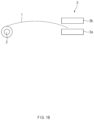
- the electrode base material to be manufactured as the single-sided electrode 1 is transferred to the punching process (the slitting process and the notching process) that is the next process in a state of being wound in the form of a roll in a state in which the active material is applied on only one surface of the electrode base material (by performing an active material drying process after the active material coating process). Also, as illustrated in FIG. 1B , the electrode base material 1 is unwound by rotation of a unwinder 2 and then supplied between an upper mold 3b and a lower mold 3a of a punching device 3.
- a curl may occur due to a difference in surface energy between a surface, on which the active material is applied, and a surface on which the active material is not applied.
- the occurrence of the curl may also occur in the electrode base material on which the active material is applied on both surfaces.
- a relatively larger curl may occur (the electrode base material is warped more severely).
- the electrode base material 1 may be not closely attached to the upper mold 3b and the lower mold 3a by the curl when the electrode base material 1 enters the punching device 3 and thus be separated to cause defects.
- KR20170048757A forming the basis for the preamble of claim 1, relates to a device for manufacturing electrode.
- JP2013216429A relates to a crease removing method, a crease removing device and a film conveying and processing device.
- a main purpose of the present invention is to provide a punching system for an electrode base material, in which the electrode base material is capable of entering a punching device in a flat state to restrict an occurrence of defects during a punching process, and a punching method.
- the air passage holes may be individually connected to an air supply device configured to inject the air and a vacuum device configured to suction the air so that each of the air passage holes independently suctions or injects the air.
- a distance measurement sensor configured to measure a distance from the surface of the electrode base material may be attached each of the upper housing and the lower housing, and the punching system may comprise a control unit configured to compare a distance between the upper housing and the surface of the electrode base material to a distance between the lower housing and the surface of the electrode base material, thereby calculating and monitoring a degree of warpage of the electrode base material.
- the distance measurement sensor may be installed at at least two or more positions on each of the upper housing and the lower housing, and the control unit may compare a degree of the warpage, which is measured first, to a degree of the warpage, which is measured later, while the electrode base material moves to determine whether to suction or inject the air through each of the air passage holes.
- the distance measurement sensor may comprise a laser distance measurement device which emits laser beam to the surface of the electrode base material to measure the distance.
- the air injected onto the surface of the electrode base material may be injected as hot air having a temperature higher than room temperature, and the air passage holes may be disposed to form rows on a surface of each of the upper housing and the lower housing, which faces the electrode base material, in horizontal and vertical directions.
- a punching method for an electrode base material according to the present invention may be additionally provided, and the punching method according to the present invention comprises: a step of supplying the electrode base material wound around a unwinder to a punching device; and a step of monitoring whether warpage of the electrode base material occurs during movement of the electrode base material to the punching device to inject or suction air onto a surface of the electrode base material when the warpage occurs so as to planarize the electrode base material.
- the warpage of the electrode base material may be calculated by comparing a value measured by a distance measurement sensor disposed at a lower side to a value measured by a distance measurement sensor disposed at an upper side while the electrode base material moves, and the air injected onto the surface of the electrode base material may be injected as hot air having a temperature higher than room temperature.
- the present invention having the above-described configuration and technical features may comprise the curl correcting device for flatting the electrode base material by injecting or suctioning the air onto the surface of the electrode base material to reduce the occurrence of defects during the punching process.
- the planarization may be realized more efficiently than the structure in which the air is injected from one side.
- the air injection amount and the air suction amount may be actively controlled according to the degree of the warpage of the electrode base material.
- the hot air may be injected onto the surface of the electrode base material to realize the planarization in the state in which the electrode base material is more flexible.
- a punching system for an electrode base material in which the electrode base material 1 coated with an active material on a surface of a collector is molded or cut in a predetermined shape is provided as a first embodiment, and a punching method for the electrode base material is provided as a second embodiment.
- a punching system comprises a unwinder 2, a punching device 3, and a curl correcting device 10.
- FIG. 2 is a simplified side view of the punching system according to a preferred embodiment of the present invention
- FIG. 4 is a simplified perspective view of a punching system
- FIG. 3 is a view illustrating a bottom surface of an upper housing illustrated in FIG. 2 (the bottom surface of the upper housing is symmetrical to a top surface of the lower housing).
- an electrode base material 1 wound in the form of a roll is mounted on the unwinder 2, and the unwinder 2 rotates the electrode base material 1 (in a direction that is opposite to a winding direction) to continuously unwind the electrode base material 1 (here, although not shown in the drawings, an additional guide device, an auxiliary drawing device, or the like may be separately mounted to guide draw-out of the electrode base material).
- the punching device 3 is disposed to be spaced a predetermined distance from the unwinder 2 and is configured to mold or cut the electrode base material 1 supplied from the unwinder 2 in a predetermined shape.
- the punching device 3 is configured to apply a pressure upward and downward so as to process the electrode base material 1 in a predetermined shape when the electrode base material 1 enters between an upper mold and a lower mode.
- the curl correcting device 10 is disposed between the unwinder 2 and the punching device 3, i.e., a moving path of the electrode base material 1. Also, while the electrode base material 1 moves to the punching device 3, the curl correcting device 10 may inject or suction air onto top and bottom surfaces of the electrode base material 1 to planarize the electrode base material 1.
- an upper housing 10b is disposed above the moving path of the electrode base material 1, and a lower housing 10a is disposed below the moving path of the electrode base material 1.
- a plurality of air passage holes 11 for injecting or suctioning air as illustrated in FIG. 3 are provided in each of surfaces (the bottom surface of the upper housing and the top surface of the lower housing) facing the surface of the electrode base material 1 to form a plurality of rows along a moving direction of the electrode base material 1 and a width direction of the electrode base material 1.
- the air passage holes 11 are individually connected to an air supply device 20 that injects air and a vacuum device that suctions air (generates a negative pressure) to independently suction or inject the air. That is, each of the air passage holes 11 may be connected to the air supply device 20 to inject air or be connected to the vacuum device 30 to suction air. Also, the respective air passage holes 11 may individually inject or suction air. However, in the case of this configuration, since hoses and valves through which air flows are complicated in configuration, the injection and the suction may be performed at the same time through the air passage holes arranged in a row unit. In an embodiment of the present invention, although the air passage holes 11 are arranged to form the rows along the moving direction of the electrode base material 1 as illustrated in FIG. 3 , the embodiment of the present invention is not limited thereto. For example, the air passage holes 11 may be formed to be concentrated in a specific area.
- the air supply device 20 may comprise an air compressor or the like which compresses air.
- the vacuum device 30 may comprise a vacuum pump that or the like which generates a negative pressure by lowering a sealed inner space to an atmospheric pressure or less.
- the hoses connecting the air supply device 20 and the vacuum device 30 to the individual air passage holes 11 have to be hermetically sealed.
- the valves that are mounted to the hoses and selectively switched may be preferably solenoid valves that are controlled by electrical signals. Also, the valves may be switched by a signal of a control unit 40.
- each of distance measurement sensors 12 that measure a distance from the surface of the electrode base material 1 is attached between the air passage holes 11 or to one side of each of the upper housing 10b and the lower housing 10b.
- the distance measurement sensors 12 are installed at at least two or more positions on each of the upper housing 10b and the lower housing 10a to continuously measure a distance between the upper housing 10b and the top surface of the electrode base material 1 and a distance between the lower housing 10a and the bottom surface of the electrode base material 1. Also, data measured by the distance measurement sensors 12 may be transmitted to the control unit 40.
- the control unit 40 may compare and calculate the received data to compare a degree of warpage, which is measured first, to a degree of warpage, which is measured later, while the electrode base material 1 moves, thereby monitoring the overall warpage shape, angle, and characteristics of the electrode base material 1 in real time.
- each of the distance measurement sensors 12 may be preferably a laser distance measurement device which emits laser beam to the surface of the electrode base material 1 to measure a distance.
- the distance measurement sensor 12 may be used without any limitation if it is a non-contact type measurement device.
- the control unit 40 determines whether to suction or inject air through each of the air passage holes 11 so that the electrode base material 1 enters the punching device 3 in a flat state according to the warpage of the electrode base material 1 to be monitored and controls the valves connected to the air supply device 20 or the vacuum device 30.
- the air discharged into the air passage holes 11 may be injected as hot air having a temperature higher than room temperature so that the electrode base material 1 more increases in flexibility. That is, air heated within the air supply device 20 may be injected, or air heated by passing through a heating wire 11a provided at an inlet-side of the air passage hole 11 may be injected. Furthermore, hot air may be injected from the front air passage holes 11, which are disposed close to the unwinder 3, and air having room temperature may be injected from the rear air passage holes 11, which are disposed close to the punching device 3, according to the warpage degree and the characteristics of the electrode base material 1. Also, since the air passage holes 11 are individually operated, as illustrated in FIG. 2 , the air may be strongly injected at the front side and relatively weakly injected at the rear side.
- a punching method for an electrode base material 1 provided as a second embodiment of the present invention is characterized in that the electrode base material 1 is continuously supplied to be punched and also is planarized before the punching.
- the punching method comprises a step of supplying an electrode base material 1 wound around a unwinder 2 to a punching device 3 while unwinding the electrode base material 1, a step of monitoring whether warpage of the electrode base material 1 occurs during movement of the electrode base material 1 to the punching device 3 to inject or suction air onto a surface of the electrode base material 1 when the warpage occurs so as to planarize the electrode base material 1, and a step of punching the planarized and entering electrode base material 1 by using the punching device 3.
- a shape and degree of warpage of the electrode base material 1 may be continuously monitored, and while the electrode base material 1 moves, a value measured by a distance measurement sensor 12 disposed at a lower side and a value measured by a distance measurement sensor 12 disposed at an upper side may be compared and calculated.
- a control unit 40 may control air to be injected or suctioned according to the warpage state to planarize the electrode base material 1 according to a previously inputted logic.
- air may be injected or suctioned onto the surface of the electrode base material 1 to planarize the electrode base material 1, thereby reducing an occurrence of defects during the punching process. Also, in the curl correcting device 10, since the air is injected or suctioned from each of the upper and lower sides of the electrode base material 1, the planarization may be realized more effectively than the structure in which the air is injected from one side.
- the air injection amount and the air suction amount may be actively controlled according to the degree of the warpage of the electrode base material 1. Furthermore, the hot air may be injected onto the surface of the electrode base material 1 to realize the planarization in the state in which the electrode base material 1 is more flexible.
Landscapes
- Engineering & Computer Science (AREA)
- Life Sciences & Earth Sciences (AREA)
- Forests & Forestry (AREA)
- Mechanical Engineering (AREA)
- Chemical & Material Sciences (AREA)
- Chemical Kinetics & Catalysis (AREA)
- Electrochemistry (AREA)
- General Chemical & Material Sciences (AREA)
- Manufacturing & Machinery (AREA)
- Battery Electrode And Active Subsutance (AREA)
Claims (10)
- Stanzsystem für ein Elektrodenbasismaterial, in welchem das Elektrodenbasismaterial (1), welches mit einem Aktivmaterial an einer Fläche eines Sammlers beschichtet ist, in einer vorbestimmten Form geformt oder geschnitten ist, wobei das Stanzsystem umfasst:einen Abwickler (2), an welchem das Elektrodenbasismaterial (1) montiert ist, welches in der Form einer Rolle gewickelt ist, und um welchen das Elektrodenbasismaterial (1) abgewickelt ist;eine Stanzvorrichtung (3), welche angeordnet ist, um eine vorbestimmte Entfernung von dem Abwickler (2) entfernt zu sein, wobei die Stanzvorrichtung (3) dazu eingerichtet ist, das Elektrodenbasismaterial (1) in einer vorbestimmten Form zu formen oder zu schneiden, welches von dem Abwickler (2) zugeführt ist; gekennzeichnet durcheine Krümmungskorrekturvorrichtung (10), welche zwischen dem Abwickler (2) und der Stanzvorrichtung (3) angeordnet ist, um Luft auf eine Fläche des Elektrodenbasismaterials (1) einzuspritzen oder zu saugen, während das Elektrodenbasismaterial (1) sich zu der Stanzvorrichtung (3) bewegt, um das Elektrodenbasismaterial zu ebnenwobei die Krümmungskorrekturvorrichtung (10) umfasst:ein oberes Gehäuse (10b), welches über einem Bewegungsweg des Elektrodenbasismaterials (1) angeordnet ist; undein unteres Gehäuse (10a), welches unter dem Bewegungspfad des Elektrodenbasismaterials (1) angeordnet ist,wobei eine Mehrzahl von Luftdurchgangslöchern (11), durch welche die Luft eingespritzt oder gesaugt ist, in jedem von dem oberen Gehäuse (10b) und dem unteren Gehäuse (10a) bereitgestellt sind.
- Stanzsystem nach Anspruch 1, wobei die Luftdurchgangslöcher (11) individuell mit einer Luftversorgungsvorrichtung (20), welche dazu eingerichtet ist, die Luft einzuspritzen, und einer Vakuumvorrichtung (30) verbunden sind, welche dazu eingerichtet ist, die Luft zu saugen, sodass jedes der Luftdurchgangslöcher (11) unabhängig die Luft saugt oder einspritzt.
- Stanzsystem nach Anspruch 2, wobei ein Entfernungsmesssensor (12), welcher dazu eingerichtet ist, eine Entfernung von der Fläche des Elektrodenbasismaterials (1) zu messen, sowohl an dem oberen Gehäuse (10a) als auch an dem unteren Gehäuse (10b) angebracht ist, und
das Stanzsystem eine Steuerungseinheit (40) umfasst, welche dazu eingerichtet ist, eine Entfernung zwischen dem oberen Gehäuse (10b) und der Fläche des Elektrodenbasismaterials (1) mit einer Entfernung zwischen dem unteren Gehäuse (10a) und der Fläche des Elektrodenbasismaterials (1) zu vergleichen, wodurch sie einen Grad einer Krümmung des Elektrodenbasismaterials (1) berechnet und überwacht. - Stanzsystem nach Anspruch 3, wobei der Entfernungsmesssensor (12) an wenigstens zwei oder mehr Positionen an sowohl dem oberen Gehäuse (10b) als auch an dem unteren Gehäuse (10a) installiert ist, und
die Steuerungseinheit (40) einen Grad der Krümmung, welcher zuerst gemessen ist, mit einem Grad der Krümmung vergleicht, welcher später gemessen ist, während das Elektrodenbasismaterial (1) sich bewegt, um zu bestimmen, ob die Luft durch jedes der Luftdurchgangslöcher (11) zu saugen oder einzuspritzen ist. - Stanzsystem nach Anspruch 3, wobei der Entfernungsmesssensor (12) eine Laserentfernungsmessvorrichtung umfasst, welche einen Laserstrahl zu der Fläche des Elektrodenbasismaterials (1) emittiert, um die Entfernung zu messen.
- Stanzsystem nach einem der Ansprüche 1 bis 5, wobei die Luft, welche auf die Fläche des Elektrodenbasismaterials (1) eingespritzt ist, als heiße Luft eingespritzt ist, welche eine Temperatur höher als Raumtemperatur aufweist.
- Stanzsystem nach einem der Ansprüche 1 bis 5, wobei die Luftdurchgangslöcher (11) angeordnet sind, um Reihen an einer Fläche von jedem von dem oberen Gehäuse (10b) und dem unteren Gehäuse (10a), welche dem Elektrodenbasismaterial (1) zugewandt ist, in horizontalen und vertikalen Richtungen zu bilden.
- Stanzverfahren für ein Elektrodenbasismaterial (1), in welchem ein Elektrodenbasismaterial (1) in einer vorbestimmten Form geformt oder geschnitten wird, wobei das Stanzverfahren das Stanzsystem nach einem der Ansprüche 1 bis 7 verwendet und umfasst:einen Schritt eines Zuführens des Elektrodenbasismaterials (1), welches um einen Abwickler (2) gewickelt ist, zu einer Stanzvorrichtung; undeinen Schritt eines Überwachens, ob eine Krümmung des Elektrodenbasismaterials (1) auftritt, während einer Bewegung des Elektrodenbasismaterials (1) zu der Stanzvorrichtung, um Luft auf eine Fläche des Elektrodenbasismaterials (1) einzuspritzen oder zu saugen, wenn die Krümmung auftritt, sodass das Elektrodenbasismaterial (1) geebnet wird.
- Stanzverfahren nach Anspruch 8, wobei die Krümmung des Elektrodenbasismaterials berechnet wird durch Vergleichen eines Wertes, welcher durch einen Entfernungsmesssensor (12) gemessen wird, welcher an einer unteren Seite angeordnet ist, mit einem Wert, welcher durch einen Entfernungsmesssensor (12) gemessen wird, welcher an einer oberen Seite angeordnet ist, während sich das Elektrodenbasismaterial bewegt.
- Stanzverfahren nach Anspruch 8, wobei die Luft, welche auf die Fläche des Elektrodenbasismaterials (1) eingespritzt wird, als heiße Luft eingespritzt wird, welche eine Temperatur höher als Raumtemperatur aufweist.
Applications Claiming Priority (2)
| Application Number | Priority Date | Filing Date | Title |
|---|---|---|---|
| KR1020180093881A KR102301669B1 (ko) | 2018-08-10 | 2018-08-10 | 전극기재의 타발시스템 및 타발방법 |
| PCT/KR2019/007984 WO2020032393A1 (ko) | 2018-08-10 | 2019-07-01 | 전극기재의 타발시스템 및 타발방법 |
Publications (3)
| Publication Number | Publication Date |
|---|---|
| EP3670123A1 EP3670123A1 (de) | 2020-06-24 |
| EP3670123A4 EP3670123A4 (de) | 2020-12-09 |
| EP3670123B1 true EP3670123B1 (de) | 2025-06-04 |
Family
ID=69415250
Family Applications (1)
| Application Number | Title | Priority Date | Filing Date |
|---|---|---|---|
| EP19846332.5A Active EP3670123B1 (de) | 2018-08-10 | 2019-07-01 | Stanzsystem für elektrodenbasismaterial und stanzverfahren |
Country Status (8)
| Country | Link |
|---|---|
| US (1) | US11394016B2 (de) |
| EP (1) | EP3670123B1 (de) |
| KR (1) | KR102301669B1 (de) |
| CN (1) | CN111093919B (de) |
| ES (1) | ES3034500T3 (de) |
| HU (1) | HUE072118T2 (de) |
| PL (1) | PL3670123T3 (de) |
| WO (1) | WO2020032393A1 (de) |
Families Citing this family (1)
| Publication number | Priority date | Publication date | Assignee | Title |
|---|---|---|---|---|
| CN118335879B (zh) * | 2023-01-10 | 2026-04-03 | 海目星激光智能装备(江苏)有限公司 | 一种电芯制造设备 |
Family Cites Families (29)
| Publication number | Priority date | Publication date | Assignee | Title |
|---|---|---|---|---|
| DE19649488A1 (de) | 1996-11-29 | 1997-11-06 | Schott Glaswerke | Vorrichtung zur Handhabung von dünnen Glasscheiben |
| JPH11223521A (ja) | 1998-02-04 | 1999-08-17 | Hiroshi Akashi | 無接触吸着具 |
| KR100885590B1 (ko) | 2004-08-05 | 2009-02-24 | 가부시키가이샤 고베 세이코쇼 | 부착물 제거 장치 |
| JP5008561B2 (ja) * | 2005-05-09 | 2012-08-22 | パナソニック株式会社 | 電極合剤ペーストの塗布方法および塗布装置 |
| KR100816443B1 (ko) | 2006-08-25 | 2008-03-27 | 하이텍교역 주식회사 | 플렉시블 인쇄회로기판의 자동 연결장치 |
| JP4896148B2 (ja) * | 2006-10-10 | 2012-03-14 | 株式会社日本設計工業 | 薄板状材料搬送装置 |
| JP2008232793A (ja) | 2007-03-20 | 2008-10-02 | Kaneka Corp | フィルムの厚み測定方法及びフィルム厚み測定装置 |
| JP4952550B2 (ja) | 2007-11-30 | 2012-06-13 | トヨタ自動車株式会社 | 搬送膜のしわ検知装置およびその方法 |
| US8541843B2 (en) | 2008-08-14 | 2013-09-24 | Nantero Inc. | Nonvolatile nanotube programmable logic devices and a nonvolatile nanotube field programmable gate array using same |
| US20120031147A1 (en) | 2009-03-03 | 2012-02-09 | Hitachi Via Mechanics, Ltd. | Method and Apparatus for Machining Thin-Film Layer of Workpiece |
| KR20110017761A (ko) | 2009-08-14 | 2011-02-22 | 에스비리모티브 주식회사 | 이차 전지용 전극판 및 이를 포함하는 이차 전지 |
| KR101658899B1 (ko) * | 2010-05-03 | 2016-09-23 | 엘지전자 주식회사 | 프레스 장치 |
| KR101191627B1 (ko) | 2010-11-26 | 2012-10-17 | 삼성에스디아이 주식회사 | 이차전지의 전극판 건조장치 및 그 제어방법 |
| KR101879162B1 (ko) | 2012-04-03 | 2018-07-16 | 가부시키가이샤 니콘 | 기판 처리 장치 |
| JP5850787B2 (ja) * | 2012-04-06 | 2016-02-03 | 株式会社アルバック | 皺取り方法、皺取り装置、フィルム搬送処理装置 |
| KR101623716B1 (ko) | 2013-10-07 | 2016-05-24 | 주식회사 엘지화학 | 프레싱 암을 포함하는 가이드 롤 장치 |
| KR101508529B1 (ko) | 2013-12-05 | 2015-04-07 | 주식회사 신화아이티 | 이차전지 리드탭의 필름 열융착 장치 |
| KR101569798B1 (ko) | 2014-01-28 | 2015-11-17 | 주식회사 디에이테크놀로지 | 이차전지의 전극 노칭장치 |
| JP6387492B2 (ja) | 2014-04-14 | 2018-09-12 | アイセル株式会社 | シートテンション機構 |
| KR101751101B1 (ko) | 2014-06-10 | 2017-06-26 | 주식회사 엘지화학 | 이차전지용 압연장치 |
| JP6476782B2 (ja) | 2014-11-18 | 2019-03-06 | 株式会社豊田自動織機 | 電極の製造方法および電極の製造装置 |
| JP2016161007A (ja) | 2015-02-27 | 2016-09-05 | 株式会社日本製鋼所 | ガス浮上ワーク支持装置および非接触ワーク支持方法 |
| JP6539069B2 (ja) * | 2015-03-09 | 2019-07-03 | 東レエンジニアリング株式会社 | 塗布装置 |
| KR101700113B1 (ko) * | 2015-05-26 | 2017-01-26 | 주식회사 디에이테크놀로지 | 이차전지용 전극 가공장치 |
| KR102026126B1 (ko) * | 2015-10-27 | 2019-09-27 | 주식회사 엘지화학 | 노칭 롤러를 포함하고 있는 전극 제조 장치 |
| US20190002604A1 (en) | 2015-12-16 | 2019-01-03 | Dic Corporation | Heteroring-containing siloxane polymer, composition containing said polymer, and electronic element |
| KR101905560B1 (ko) * | 2016-03-08 | 2018-11-21 | 현대자동차 주식회사 | 연료전지용 막-전극 어셈블리의 제조장치 및 방법 |
| JP2018043253A (ja) | 2016-09-13 | 2018-03-22 | パナソニックIpマネジメント株式会社 | レーザ切断装置およびレーザ切断方法 |
| US20190081317A1 (en) * | 2017-09-11 | 2019-03-14 | Andreas Keil | Web coating and calendering system and method |
-
2018
- 2018-08-10 KR KR1020180093881A patent/KR102301669B1/ko active Active
-
2019
- 2019-07-01 EP EP19846332.5A patent/EP3670123B1/de active Active
- 2019-07-01 CN CN201980004315.4A patent/CN111093919B/zh active Active
- 2019-07-01 HU HUE19846332A patent/HUE072118T2/hu unknown
- 2019-07-01 PL PL19846332.5T patent/PL3670123T3/pl unknown
- 2019-07-01 WO PCT/KR2019/007984 patent/WO2020032393A1/ko not_active Ceased
- 2019-07-01 US US16/649,439 patent/US11394016B2/en active Active
- 2019-07-01 ES ES19846332T patent/ES3034500T3/es active Active
Also Published As
| Publication number | Publication date |
|---|---|
| ES3034500T3 (en) | 2025-08-19 |
| PL3670123T3 (pl) | 2025-08-11 |
| EP3670123A1 (de) | 2020-06-24 |
| KR20200018092A (ko) | 2020-02-19 |
| CN111093919B (zh) | 2022-01-04 |
| HUE072118T2 (hu) | 2025-10-28 |
| CN111093919A (zh) | 2020-05-01 |
| US20200274136A1 (en) | 2020-08-27 |
| KR102301669B1 (ko) | 2021-09-14 |
| US11394016B2 (en) | 2022-07-19 |
| WO2020032393A1 (ko) | 2020-02-13 |
| EP3670123A4 (de) | 2020-12-09 |
Similar Documents
| Publication | Publication Date | Title |
|---|---|---|
| EP2973835B1 (de) | Elektrochemische zelle mit gefalteter elektrode und separator, batterie damit und verfahren zur herstellung davon | |
| CN108140903B (zh) | 二次电池及其制造方法 | |
| JP2014164982A (ja) | 電池用電極、電池、電池用電極の製造方法および電池用電極の製造装置 | |
| WO2016186209A1 (ja) | 二次電池用の電極および二次電池の製造方法と製造装置 | |
| EP3670123B1 (de) | Stanzsystem für elektrodenbasismaterial und stanzverfahren | |
| US20190103598A1 (en) | Method of manufacturing battery electrode and electrode manufacturing apparatus | |
| KR20210124703A (ko) | 이차전지의 전극 제조 시 사용되는 전극용 원단의 이송장치 | |
| KR101789854B1 (ko) | 이차전지 사행 불량 판정 시스템 및 그 방법 | |
| KR102914055B1 (ko) | 단위 셀 제조 장치 및 방법 | |
| KR20170112390A (ko) | 이차전지용 코팅 전극 제조 장치 및 그 제조 방법 | |
| KR101750594B1 (ko) | 이차전지의 음극 코팅층 두께 측정 시스템 | |
| KR100696811B1 (ko) | 이차전지의 전극롤 권취 방법 | |
| KR20180115152A (ko) | 잔류응력 편차 해소를 위한 전지의 단위 전극 및 그를 포함하는 리튬 이온 폴리머 전지 | |
| KR100646550B1 (ko) | 이차 전지의 전극판과 이차 전지의 전극판 코팅 장치 | |
| KR20240111595A (ko) | 전극 제조 장치 및 방법 | |
| KR20050096290A (ko) | 내부 단락을 방지할 수 있는 이차 전지 | |
| US20230061588A1 (en) | Electrode Rolling Apparatus and Electrode Rolling Method | |
| CN104766941B (zh) | 用于蓄电池单元的电极 | |
| US12506178B2 (en) | Electrode assembly comprising adhesive on separator sheet and apparatus and method for manufacturing the same | |
| KR102959882B1 (ko) | 전극적층체 및 이의 제조방법 | |
| US20250279457A1 (en) | Electrode Assembly Joining Device, Electrode Assembly Manufacturing Device Comprising Same, Electrode Assembly Joining Method, and Electrode Assembly Manufacturing Method | |
| EP4566724A1 (de) | Schlitzdüse zur herstellung einer wiederaufladbaren batterieelektrode, wiederaufladbare batterieelektrode und herstellungsverfahren damit | |
| EP4618166A1 (de) | Vorrichtung und verfahren zur herstellung einer elektrode | |
| KR20260040877A (ko) | 전극코팅장치 | |
| KR20230127059A (ko) | 히팅 장치 |
Legal Events
| Date | Code | Title | Description |
|---|---|---|---|
| STAA | Information on the status of an ep patent application or granted ep patent |
Free format text: STATUS: THE INTERNATIONAL PUBLICATION HAS BEEN MADE |
|
| PUAI | Public reference made under article 153(3) epc to a published international application that has entered the european phase |
Free format text: ORIGINAL CODE: 0009012 |
|
| STAA | Information on the status of an ep patent application or granted ep patent |
Free format text: STATUS: REQUEST FOR EXAMINATION WAS MADE |
|
| 17P | Request for examination filed |
Effective date: 20200320 |
|
| AK | Designated contracting states |
Kind code of ref document: A1 Designated state(s): AL AT BE BG CH CY CZ DE DK EE ES FI FR GB GR HR HU IE IS IT LI LT LU LV MC MK MT NL NO PL PT RO RS SE SI SK SM TR |
|
| AX | Request for extension of the european patent |
Extension state: BA ME |
|
| A4 | Supplementary search report drawn up and despatched |
Effective date: 20201105 |
|
| RIC1 | Information provided on ipc code assigned before grant |
Ipc: B26D 7/01 20060101ALI20201030BHEP Ipc: B26F 1/40 20060101AFI20201030BHEP Ipc: B26D 7/27 20060101ALI20201030BHEP |
|
| DAV | Request for validation of the european patent (deleted) | ||
| DAX | Request for extension of the european patent (deleted) | ||
| RAP1 | Party data changed (applicant data changed or rights of an application transferred) |
Owner name: LG ENERGY SOLUTION LTD. |
|
| RAP3 | Party data changed (applicant data changed or rights of an application transferred) |
Owner name: LG ENERGY SOLUTION, LTD. |
|
| STAA | Information on the status of an ep patent application or granted ep patent |
Free format text: STATUS: EXAMINATION IS IN PROGRESS |
|
| 17Q | First examination report despatched |
Effective date: 20221102 |
|
| GRAP | Despatch of communication of intention to grant a patent |
Free format text: ORIGINAL CODE: EPIDOSNIGR1 |
|
| STAA | Information on the status of an ep patent application or granted ep patent |
Free format text: STATUS: GRANT OF PATENT IS INTENDED |
|
| INTG | Intention to grant announced |
Effective date: 20250328 |
|
| GRAS | Grant fee paid |
Free format text: ORIGINAL CODE: EPIDOSNIGR3 |
|
| GRAA | (expected) grant |
Free format text: ORIGINAL CODE: 0009210 |
|
| STAA | Information on the status of an ep patent application or granted ep patent |
Free format text: STATUS: THE PATENT HAS BEEN GRANTED |
|
| P01 | Opt-out of the competence of the unified patent court (upc) registered |
Free format text: CASE NUMBER: APP_16825/2025 Effective date: 20250407 |
|
| AK | Designated contracting states |
Kind code of ref document: B1 Designated state(s): AL AT BE BG CH CY CZ DE DK EE ES FI FR GB GR HR HU IE IS IT LI LT LU LV MC MK MT NL NO PL PT RO RS SE SI SK SM TR |
|
| REG | Reference to a national code |
Ref country code: GB Ref legal event code: FG4D |
|
| REG | Reference to a national code |
Ref country code: CH Ref legal event code: EP |
|
| REG | Reference to a national code |
Ref country code: DE Ref legal event code: R096 Ref document number: 602019070860 Country of ref document: DE |
|
| REG | Reference to a national code |
Ref country code: IE Ref legal event code: FG4D |
|
| PGFP | Annual fee paid to national office [announced via postgrant information from national office to epo] |
Ref country code: GB Payment date: 20250624 Year of fee payment: 7 |
|
| PGFP | Annual fee paid to national office [announced via postgrant information from national office to epo] |
Ref country code: BE Payment date: 20250623 Year of fee payment: 7 |
|
| PGFP | Annual fee paid to national office [announced via postgrant information from national office to epo] |
Ref country code: FR Payment date: 20250624 Year of fee payment: 7 |
|
| REG | Reference to a national code |
Ref country code: SE Ref legal event code: TRGR |
|
| PGFP | Annual fee paid to national office [announced via postgrant information from national office to epo] |
Ref country code: SE Payment date: 20250624 Year of fee payment: 7 |
|
| REG | Reference to a national code |
Ref country code: ES Ref legal event code: FG2A Ref document number: 3034500 Country of ref document: ES Kind code of ref document: T3 Effective date: 20250819 |
|
| REG | Reference to a national code |
Ref country code: NL Ref legal event code: MP Effective date: 20250604 |
|
| PG25 | Lapsed in a contracting state [announced via postgrant information from national office to epo] |
Ref country code: FI Free format text: LAPSE BECAUSE OF FAILURE TO SUBMIT A TRANSLATION OF THE DESCRIPTION OR TO PAY THE FEE WITHIN THE PRESCRIBED TIME-LIMIT Effective date: 20250604 |
|
| PGFP | Annual fee paid to national office [announced via postgrant information from national office to epo] |
Ref country code: ES Payment date: 20250822 Year of fee payment: 7 |
|
| PGFP | Annual fee paid to national office [announced via postgrant information from national office to epo] |
Ref country code: DE Payment date: 20250624 Year of fee payment: 7 |
|
| REG | Reference to a national code |
Ref country code: LT Ref legal event code: MG9D |
|
| PG25 | Lapsed in a contracting state [announced via postgrant information from national office to epo] |
Ref country code: GR Free format text: LAPSE BECAUSE OF FAILURE TO SUBMIT A TRANSLATION OF THE DESCRIPTION OR TO PAY THE FEE WITHIN THE PRESCRIBED TIME-LIMIT Effective date: 20250905 Ref country code: NO Free format text: LAPSE BECAUSE OF FAILURE TO SUBMIT A TRANSLATION OF THE DESCRIPTION OR TO PAY THE FEE WITHIN THE PRESCRIBED TIME-LIMIT Effective date: 20250904 |
|
| PGFP | Annual fee paid to national office [announced via postgrant information from national office to epo] |
Ref country code: PL Payment date: 20250625 Year of fee payment: 7 |
|
| PG25 | Lapsed in a contracting state [announced via postgrant information from national office to epo] |
Ref country code: BG Free format text: LAPSE BECAUSE OF FAILURE TO SUBMIT A TRANSLATION OF THE DESCRIPTION OR TO PAY THE FEE WITHIN THE PRESCRIBED TIME-LIMIT Effective date: 20250604 |
|
| PGFP | Annual fee paid to national office [announced via postgrant information from national office to epo] |
Ref country code: HU Payment date: 20250929 Year of fee payment: 7 |
|
| PG25 | Lapsed in a contracting state [announced via postgrant information from national office to epo] |
Ref country code: HR Free format text: LAPSE BECAUSE OF FAILURE TO SUBMIT A TRANSLATION OF THE DESCRIPTION OR TO PAY THE FEE WITHIN THE PRESCRIBED TIME-LIMIT Effective date: 20250604 |
|
| PG25 | Lapsed in a contracting state [announced via postgrant information from national office to epo] |
Ref country code: RS Free format text: LAPSE BECAUSE OF FAILURE TO SUBMIT A TRANSLATION OF THE DESCRIPTION OR TO PAY THE FEE WITHIN THE PRESCRIBED TIME-LIMIT Effective date: 20250904 |
|
| REG | Reference to a national code |
Ref country code: HU Ref legal event code: AG4A Ref document number: E072118 Country of ref document: HU |
|
| PG25 | Lapsed in a contracting state [announced via postgrant information from national office to epo] |
Ref country code: LV Free format text: LAPSE BECAUSE OF FAILURE TO SUBMIT A TRANSLATION OF THE DESCRIPTION OR TO PAY THE FEE WITHIN THE PRESCRIBED TIME-LIMIT Effective date: 20250604 |
|
| PG25 | Lapsed in a contracting state [announced via postgrant information from national office to epo] |
Ref country code: NL Free format text: LAPSE BECAUSE OF FAILURE TO SUBMIT A TRANSLATION OF THE DESCRIPTION OR TO PAY THE FEE WITHIN THE PRESCRIBED TIME-LIMIT Effective date: 20250604 |
|
| PG25 | Lapsed in a contracting state [announced via postgrant information from national office to epo] |
Ref country code: PT Free format text: LAPSE BECAUSE OF FAILURE TO SUBMIT A TRANSLATION OF THE DESCRIPTION OR TO PAY THE FEE WITHIN THE PRESCRIBED TIME-LIMIT Effective date: 20251006 |
|
| REG | Reference to a national code |
Ref country code: AT Ref legal event code: MK05 Ref document number: 1799936 Country of ref document: AT Kind code of ref document: T Effective date: 20250604 |
|
| PG25 | Lapsed in a contracting state [announced via postgrant information from national office to epo] |
Ref country code: IS Free format text: LAPSE BECAUSE OF FAILURE TO SUBMIT A TRANSLATION OF THE DESCRIPTION OR TO PAY THE FEE WITHIN THE PRESCRIBED TIME-LIMIT Effective date: 20251004 |
|
| PG25 | Lapsed in a contracting state [announced via postgrant information from national office to epo] |
Ref country code: SM Free format text: LAPSE BECAUSE OF FAILURE TO SUBMIT A TRANSLATION OF THE DESCRIPTION OR TO PAY THE FEE WITHIN THE PRESCRIBED TIME-LIMIT Effective date: 20250604 Ref country code: AT Free format text: LAPSE BECAUSE OF FAILURE TO SUBMIT A TRANSLATION OF THE DESCRIPTION OR TO PAY THE FEE WITHIN THE PRESCRIBED TIME-LIMIT Effective date: 20250604 |
|
| PG25 | Lapsed in a contracting state [announced via postgrant information from national office to epo] |
Ref country code: CZ Free format text: LAPSE BECAUSE OF FAILURE TO SUBMIT A TRANSLATION OF THE DESCRIPTION OR TO PAY THE FEE WITHIN THE PRESCRIBED TIME-LIMIT Effective date: 20250604 |
|
| PG25 | Lapsed in a contracting state [announced via postgrant information from national office to epo] |
Ref country code: EE Free format text: LAPSE BECAUSE OF FAILURE TO SUBMIT A TRANSLATION OF THE DESCRIPTION OR TO PAY THE FEE WITHIN THE PRESCRIBED TIME-LIMIT Effective date: 20250604 |
|
| PG25 | Lapsed in a contracting state [announced via postgrant information from national office to epo] |
Ref country code: RO Free format text: LAPSE BECAUSE OF FAILURE TO SUBMIT A TRANSLATION OF THE DESCRIPTION OR TO PAY THE FEE WITHIN THE PRESCRIBED TIME-LIMIT Effective date: 20250604 Ref country code: SK Free format text: LAPSE BECAUSE OF FAILURE TO SUBMIT A TRANSLATION OF THE DESCRIPTION OR TO PAY THE FEE WITHIN THE PRESCRIBED TIME-LIMIT Effective date: 20250604 |
|
| PG25 | Lapsed in a contracting state [announced via postgrant information from national office to epo] |
Ref country code: IT Free format text: LAPSE BECAUSE OF FAILURE TO SUBMIT A TRANSLATION OF THE DESCRIPTION OR TO PAY THE FEE WITHIN THE PRESCRIBED TIME-LIMIT Effective date: 20250604 |
|
| REG | Reference to a national code |
Ref country code: CH Ref legal event code: H13 Free format text: ST27 STATUS EVENT CODE: U-0-0-H10-H13 (AS PROVIDED BY THE NATIONAL OFFICE) Effective date: 20260224 |
|
| REG | Reference to a national code |
Ref country code: DE Ref legal event code: R097 Ref document number: 602019070860 Country of ref document: DE |
|
| PG25 | Lapsed in a contracting state [announced via postgrant information from national office to epo] |
Ref country code: LU Free format text: LAPSE BECAUSE OF NON-PAYMENT OF DUE FEES Effective date: 20250701 |
|
| PG25 | Lapsed in a contracting state [announced via postgrant information from national office to epo] |
Ref country code: MC Free format text: LAPSE BECAUSE OF FAILURE TO SUBMIT A TRANSLATION OF THE DESCRIPTION OR TO PAY THE FEE WITHIN THE PRESCRIBED TIME-LIMIT Effective date: 20250604 |
|
| PLBE | No opposition filed within time limit |
Free format text: ORIGINAL CODE: 0009261 |
|
| STAA | Information on the status of an ep patent application or granted ep patent |
Free format text: STATUS: NO OPPOSITION FILED WITHIN TIME LIMIT |
|
| PG25 | Lapsed in a contracting state [announced via postgrant information from national office to epo] |
Ref country code: DK Free format text: LAPSE BECAUSE OF FAILURE TO SUBMIT A TRANSLATION OF THE DESCRIPTION OR TO PAY THE FEE WITHIN THE PRESCRIBED TIME-LIMIT Effective date: 20250604 |
|
| REG | Reference to a national code |
Ref country code: CH Ref legal event code: L10 Free format text: ST27 STATUS EVENT CODE: U-0-0-L10-L00 (AS PROVIDED BY THE NATIONAL OFFICE) Effective date: 20260416 |
|
| PG25 | Lapsed in a contracting state [announced via postgrant information from national office to epo] |
Ref country code: CH Free format text: LAPSE BECAUSE OF NON-PAYMENT OF DUE FEES Effective date: 20250731 |