EP3663733A1 - Detecteur thermique a membrane suspendue comportant une partie deformable de court-circuit thermique - Google Patents
Detecteur thermique a membrane suspendue comportant une partie deformable de court-circuit thermique Download PDFInfo
- Publication number
- EP3663733A1 EP3663733A1 EP19211794.3A EP19211794A EP3663733A1 EP 3663733 A1 EP3663733 A1 EP 3663733A1 EP 19211794 A EP19211794 A EP 19211794A EP 3663733 A1 EP3663733 A1 EP 3663733A1
- Authority
- EP
- European Patent Office
- Prior art keywords
- substrate
- temperature
- contact
- free end
- absorbent membrane
- Prior art date
- Legal status (The legal status is an assumption and is not a legal conclusion. Google has not performed a legal analysis and makes no representation as to the accuracy of the status listed.)
- Withdrawn
Links
- 239000012528 membrane Substances 0.000 title claims abstract description 108
- 239000000758 substrate Substances 0.000 claims abstract description 124
- 230000002745 absorbent Effects 0.000 claims abstract description 95
- 239000002250 absorbent Substances 0.000 claims abstract description 95
- 229910001285 shape-memory alloy Inorganic materials 0.000 claims abstract description 46
- 229910000734 martensite Inorganic materials 0.000 claims description 59
- 230000009466 transformation Effects 0.000 claims description 30
- 238000001514 detection method Methods 0.000 claims description 29
- 230000005670 electromagnetic radiation Effects 0.000 claims description 23
- 238000004873 anchoring Methods 0.000 claims description 22
- 238000009413 insulation Methods 0.000 claims description 13
- 229910045601 alloy Inorganic materials 0.000 claims description 10
- 239000000956 alloy Substances 0.000 claims description 10
- 238000004519 manufacturing process Methods 0.000 claims description 8
- 229910001092 metal group alloy Inorganic materials 0.000 claims description 8
- 239000004020 conductor Substances 0.000 claims description 7
- 230000002441 reversible effect Effects 0.000 claims description 7
- 230000000694 effects Effects 0.000 claims description 6
- 229910052719 titanium Inorganic materials 0.000 claims description 6
- 229910001000 nickel titanium Inorganic materials 0.000 claims description 5
- 238000000151 deposition Methods 0.000 claims description 2
- 239000010410 layer Substances 0.000 description 60
- 239000012071 phase Substances 0.000 description 46
- 238000001816 cooling Methods 0.000 description 26
- 239000000463 material Substances 0.000 description 22
- 238000010438 heat treatment Methods 0.000 description 18
- PXHVJJICTQNCMI-UHFFFAOYSA-N nickel Substances [Ni] PXHVJJICTQNCMI-UHFFFAOYSA-N 0.000 description 15
- 239000010949 copper Substances 0.000 description 14
- 230000007423 decrease Effects 0.000 description 14
- 239000010936 titanium Substances 0.000 description 14
- KRHYYFGTRYWZRS-UHFFFAOYSA-N hydrofluoric acid Substances F KRHYYFGTRYWZRS-UHFFFAOYSA-N 0.000 description 13
- 230000010355 oscillation Effects 0.000 description 12
- 229910001566 austenite Inorganic materials 0.000 description 11
- 229910021417 amorphous silicon Inorganic materials 0.000 description 9
- 229910052500 inorganic mineral Inorganic materials 0.000 description 9
- 239000011707 mineral Substances 0.000 description 9
- 239000011241 protective layer Substances 0.000 description 9
- RYGMFSIKBFXOCR-UHFFFAOYSA-N Copper Chemical compound [Cu] RYGMFSIKBFXOCR-UHFFFAOYSA-N 0.000 description 7
- 229910052802 copper Inorganic materials 0.000 description 7
- 230000005855 radiation Effects 0.000 description 7
- XEEYBQQBJWHFJM-UHFFFAOYSA-N Iron Chemical compound [Fe] XEEYBQQBJWHFJM-UHFFFAOYSA-N 0.000 description 6
- 229910052751 metal Inorganic materials 0.000 description 6
- 239000002184 metal Substances 0.000 description 6
- WFKWXMTUELFFGS-UHFFFAOYSA-N tungsten Chemical compound [W] WFKWXMTUELFFGS-UHFFFAOYSA-N 0.000 description 6
- 238000005530 etching Methods 0.000 description 5
- QPJSUIGXIBEQAC-UHFFFAOYSA-N n-(2,4-dichloro-5-propan-2-yloxyphenyl)acetamide Chemical compound CC(C)OC1=CC(NC(C)=O)=C(Cl)C=C1Cl QPJSUIGXIBEQAC-UHFFFAOYSA-N 0.000 description 5
- KDLHZDBZIXYQEI-UHFFFAOYSA-N palladium Substances [Pd] KDLHZDBZIXYQEI-UHFFFAOYSA-N 0.000 description 5
- 239000000126 substance Substances 0.000 description 5
- 229910052721 tungsten Inorganic materials 0.000 description 5
- 239000010937 tungsten Substances 0.000 description 5
- 229910018072 Al 2 O 3 Inorganic materials 0.000 description 4
- 239000006096 absorbing agent Substances 0.000 description 4
- 230000015572 biosynthetic process Effects 0.000 description 4
- 239000003989 dielectric material Substances 0.000 description 4
- 239000011159 matrix material Substances 0.000 description 4
- 238000000034 method Methods 0.000 description 4
- BASFCYQUMIYNBI-UHFFFAOYSA-N platinum Chemical compound [Pt] BASFCYQUMIYNBI-UHFFFAOYSA-N 0.000 description 4
- 230000010287 polarization Effects 0.000 description 4
- 230000004044 response Effects 0.000 description 4
- 230000002123 temporal effect Effects 0.000 description 4
- 229910001935 vanadium oxide Inorganic materials 0.000 description 4
- ATJFFYVFTNAWJD-UHFFFAOYSA-N Tin Chemical compound [Sn] ATJFFYVFTNAWJD-UHFFFAOYSA-N 0.000 description 3
- RTAQQCXQSZGOHL-UHFFFAOYSA-N Titanium Chemical compound [Ti] RTAQQCXQSZGOHL-UHFFFAOYSA-N 0.000 description 3
- NRTOMJZYCJJWKI-UHFFFAOYSA-N Titanium nitride Chemical compound [Ti]#N NRTOMJZYCJJWKI-UHFFFAOYSA-N 0.000 description 3
- 239000002253 acid Substances 0.000 description 3
- 229910052782 aluminium Inorganic materials 0.000 description 3
- XAGFODPZIPBFFR-UHFFFAOYSA-N aluminium Chemical compound [Al] XAGFODPZIPBFFR-UHFFFAOYSA-N 0.000 description 3
- 230000015556 catabolic process Effects 0.000 description 3
- 229910052729 chemical element Inorganic materials 0.000 description 3
- PMHQVHHXPFUNSP-UHFFFAOYSA-M copper(1+);methylsulfanylmethane;bromide Chemical compound Br[Cu].CSC PMHQVHHXPFUNSP-UHFFFAOYSA-M 0.000 description 3
- 238000006731 degradation reaction Methods 0.000 description 3
- 230000006870 function Effects 0.000 description 3
- 229910010272 inorganic material Inorganic materials 0.000 description 3
- 239000011147 inorganic material Substances 0.000 description 3
- 239000007769 metal material Substances 0.000 description 3
- 230000036961 partial effect Effects 0.000 description 3
- 238000005240 physical vapour deposition Methods 0.000 description 3
- 239000012808 vapor phase Substances 0.000 description 3
- 229910052727 yttrium Inorganic materials 0.000 description 3
- 229910017083 AlN Inorganic materials 0.000 description 2
- VYPSYNLAJGMNEJ-UHFFFAOYSA-N Silicium dioxide Chemical compound O=[Si]=O VYPSYNLAJGMNEJ-UHFFFAOYSA-N 0.000 description 2
- XUIMIQQOPSSXEZ-UHFFFAOYSA-N Silicon Chemical compound [Si] XUIMIQQOPSSXEZ-UHFFFAOYSA-N 0.000 description 2
- GWEVSGVZZGPLCZ-UHFFFAOYSA-N Titan oxide Chemical compound O=[Ti]=O GWEVSGVZZGPLCZ-UHFFFAOYSA-N 0.000 description 2
- XHCLAFWTIXFWPH-UHFFFAOYSA-N [O-2].[O-2].[O-2].[O-2].[O-2].[V+5].[V+5] Chemical compound [O-2].[O-2].[O-2].[O-2].[O-2].[V+5].[V+5] XHCLAFWTIXFWPH-UHFFFAOYSA-N 0.000 description 2
- 238000010521 absorption reaction Methods 0.000 description 2
- PNEYBMLMFCGWSK-UHFFFAOYSA-N aluminium oxide Inorganic materials [O-2].[O-2].[O-2].[Al+3].[Al+3] PNEYBMLMFCGWSK-UHFFFAOYSA-N 0.000 description 2
- 230000008901 benefit Effects 0.000 description 2
- 239000003990 capacitor Substances 0.000 description 2
- 238000005229 chemical vapour deposition Methods 0.000 description 2
- 150000001875 compounds Chemical class 0.000 description 2
- 230000006866 deterioration Effects 0.000 description 2
- 238000001312 dry etching Methods 0.000 description 2
- 239000010931 gold Substances 0.000 description 2
- 229910052742 iron Inorganic materials 0.000 description 2
- 239000002070 nanowire Substances 0.000 description 2
- 229910052759 nickel Inorganic materials 0.000 description 2
- 229910052710 silicon Inorganic materials 0.000 description 2
- 239000010703 silicon Substances 0.000 description 2
- LIVNPJMFVYWSIS-UHFFFAOYSA-N silicon monoxide Chemical compound [Si-]#[O+] LIVNPJMFVYWSIS-UHFFFAOYSA-N 0.000 description 2
- 229910052814 silicon oxide Inorganic materials 0.000 description 2
- 239000000725 suspension Substances 0.000 description 2
- OGIDPMRJRNCKJF-UHFFFAOYSA-N titanium oxide Inorganic materials [Ti]=O OGIDPMRJRNCKJF-UHFFFAOYSA-N 0.000 description 2
- GPPXJZIENCGNKB-UHFFFAOYSA-N vanadium Chemical compound [V]#[V] GPPXJZIENCGNKB-UHFFFAOYSA-N 0.000 description 2
- 238000003631 wet chemical etching Methods 0.000 description 2
- KLZUFWVZNOTSEM-UHFFFAOYSA-K Aluminium flouride Chemical compound F[Al](F)F KLZUFWVZNOTSEM-UHFFFAOYSA-K 0.000 description 1
- OKTJSMMVPCPJKN-UHFFFAOYSA-N Carbon Chemical compound [C] OKTJSMMVPCPJKN-UHFFFAOYSA-N 0.000 description 1
- 229910002515 CoAl Inorganic materials 0.000 description 1
- KRHYYFGTRYWZRS-UHFFFAOYSA-M Fluoride anion Chemical compound [F-] KRHYYFGTRYWZRS-UHFFFAOYSA-M 0.000 description 1
- 241000796194 Nitia Species 0.000 description 1
- 239000004642 Polyimide Substances 0.000 description 1
- 229910052581 Si3N4 Inorganic materials 0.000 description 1
- QCWXUUIWCKQGHC-UHFFFAOYSA-N Zirconium Chemical compound [Zr] QCWXUUIWCKQGHC-UHFFFAOYSA-N 0.000 description 1
- 230000032683 aging Effects 0.000 description 1
- 229910003481 amorphous carbon Inorganic materials 0.000 description 1
- 230000008859 change Effects 0.000 description 1
- 239000003610 charcoal Substances 0.000 description 1
- 238000003486 chemical etching Methods 0.000 description 1
- 239000003795 chemical substances by application Substances 0.000 description 1
- 239000003245 coal Substances 0.000 description 1
- 230000001419 dependent effect Effects 0.000 description 1
- 230000001627 detrimental effect Effects 0.000 description 1
- 238000006073 displacement reaction Methods 0.000 description 1
- 230000005669 field effect Effects 0.000 description 1
- PCHJSUWPFVWCPO-UHFFFAOYSA-N gold Chemical compound [Au] PCHJSUWPFVWCPO-UHFFFAOYSA-N 0.000 description 1
- 229910052737 gold Inorganic materials 0.000 description 1
- 229910052735 hafnium Inorganic materials 0.000 description 1
- VBJZVLUMGGDVMO-UHFFFAOYSA-N hafnium atom Chemical compound [Hf] VBJZVLUMGGDVMO-UHFFFAOYSA-N 0.000 description 1
- 238000003384 imaging method Methods 0.000 description 1
- 238000009434 installation Methods 0.000 description 1
- 238000002955 isolation Methods 0.000 description 1
- 230000000670 limiting effect Effects 0.000 description 1
- 229910044991 metal oxide Inorganic materials 0.000 description 1
- 150000004706 metal oxides Chemical class 0.000 description 1
- 230000004048 modification Effects 0.000 description 1
- 238000012986 modification Methods 0.000 description 1
- TWNQGVIAIRXVLR-UHFFFAOYSA-N oxo(oxoalumanyloxy)alumane Chemical compound O=[Al]O[Al]=O TWNQGVIAIRXVLR-UHFFFAOYSA-N 0.000 description 1
- 229910052763 palladium Inorganic materials 0.000 description 1
- 238000000206 photolithography Methods 0.000 description 1
- 238000000623 plasma-assisted chemical vapour deposition Methods 0.000 description 1
- 229910052697 platinum Inorganic materials 0.000 description 1
- 229920001721 polyimide Polymers 0.000 description 1
- 230000008569 process Effects 0.000 description 1
- 230000000750 progressive effect Effects 0.000 description 1
- 230000001681 protective effect Effects 0.000 description 1
- 230000002829 reductive effect Effects 0.000 description 1
- 239000004065 semiconductor Substances 0.000 description 1
- HBMJWWWQQXIZIP-UHFFFAOYSA-N silicon carbide Chemical compound [Si+]#[C-] HBMJWWWQQXIZIP-UHFFFAOYSA-N 0.000 description 1
- 229910010271 silicon carbide Inorganic materials 0.000 description 1
- HQVNEWCFYHHQES-UHFFFAOYSA-N silicon nitride Chemical compound N12[Si]34N5[Si]62N3[Si]51N64 HQVNEWCFYHHQES-UHFFFAOYSA-N 0.000 description 1
- 230000035882 stress Effects 0.000 description 1
- 230000001629 suppression Effects 0.000 description 1
- 229910052715 tantalum Inorganic materials 0.000 description 1
- GUVRBAGPIYLISA-UHFFFAOYSA-N tantalum atom Chemical compound [Ta] GUVRBAGPIYLISA-UHFFFAOYSA-N 0.000 description 1
- 238000001931 thermography Methods 0.000 description 1
- 239000010409 thin film Substances 0.000 description 1
- 230000007704 transition Effects 0.000 description 1
- 238000001039 wet etching Methods 0.000 description 1
- 229910052726 zirconium Inorganic materials 0.000 description 1
Images


Classifications
-
- G—PHYSICS
- G01—MEASURING; TESTING
- G01J—MEASUREMENT OF INTENSITY, VELOCITY, SPECTRAL CONTENT, POLARISATION, PHASE OR PULSE CHARACTERISTICS OF INFRARED, VISIBLE OR ULTRAVIOLET LIGHT; COLORIMETRY; RADIATION PYROMETRY
- G01J5/00—Radiation pyrometry, e.g. infrared or optical thermometry
- G01J5/02—Constructional details
- G01J5/04—Casings
- G01J5/046—Materials; Selection of thermal materials
-
- G—PHYSICS
- G01—MEASURING; TESTING
- G01J—MEASUREMENT OF INTENSITY, VELOCITY, SPECTRAL CONTENT, POLARISATION, PHASE OR PULSE CHARACTERISTICS OF INFRARED, VISIBLE OR ULTRAVIOLET LIGHT; COLORIMETRY; RADIATION PYROMETRY
- G01J5/00—Radiation pyrometry, e.g. infrared or optical thermometry
- G01J5/02—Constructional details
- G01J5/0225—Shape of the cavity itself or of elements contained in or suspended over the cavity
- G01J5/0245—Shape of the cavity itself or of elements contained in or suspended over the cavity for performing thermal shunt
-
- G—PHYSICS
- G01—MEASURING; TESTING
- G01J—MEASUREMENT OF INTENSITY, VELOCITY, SPECTRAL CONTENT, POLARISATION, PHASE OR PULSE CHARACTERISTICS OF INFRARED, VISIBLE OR ULTRAVIOLET LIGHT; COLORIMETRY; RADIATION PYROMETRY
- G01J5/00—Radiation pyrometry, e.g. infrared or optical thermometry
- G01J5/02—Constructional details
- G01J5/021—Probe covers for thermometers, e.g. tympanic thermometers; Containers for probe covers; Disposable probes
-
- G—PHYSICS
- G01—MEASURING; TESTING
- G01J—MEASUREMENT OF INTENSITY, VELOCITY, SPECTRAL CONTENT, POLARISATION, PHASE OR PULSE CHARACTERISTICS OF INFRARED, VISIBLE OR ULTRAVIOLET LIGHT; COLORIMETRY; RADIATION PYROMETRY
- G01J5/00—Radiation pyrometry, e.g. infrared or optical thermometry
- G01J5/02—Constructional details
- G01J5/0215—Compact construction
-
- G—PHYSICS
- G01—MEASURING; TESTING
- G01J—MEASUREMENT OF INTENSITY, VELOCITY, SPECTRAL CONTENT, POLARISATION, PHASE OR PULSE CHARACTERISTICS OF INFRARED, VISIBLE OR ULTRAVIOLET LIGHT; COLORIMETRY; RADIATION PYROMETRY
- G01J5/00—Radiation pyrometry, e.g. infrared or optical thermometry
- G01J5/10—Radiation pyrometry, e.g. infrared or optical thermometry using electric radiation detectors
- G01J5/20—Radiation pyrometry, e.g. infrared or optical thermometry using electric radiation detectors using resistors, thermistors or semiconductors sensitive to radiation, e.g. photoconductive devices
-
- G—PHYSICS
- G01—MEASURING; TESTING
- G01J—MEASUREMENT OF INTENSITY, VELOCITY, SPECTRAL CONTENT, POLARISATION, PHASE OR PULSE CHARACTERISTICS OF INFRARED, VISIBLE OR ULTRAVIOLET LIGHT; COLORIMETRY; RADIATION PYROMETRY
- G01J5/00—Radiation pyrometry, e.g. infrared or optical thermometry
- G01J5/38—Radiation pyrometry, e.g. infrared or optical thermometry using extension or expansion of solids or fluids
- G01J5/40—Radiation pyrometry, e.g. infrared or optical thermometry using extension or expansion of solids or fluids using bimaterial elements
Definitions
- the field of the invention is that of thermal detectors of electromagnetic radiation, for example infrared or terahertz, comprising an absorbent membrane suspended and thermally isolated from the substrate.
- the invention applies in particular to the field of infrared or terahertz imaging, thermography, or even the detection of people or of movement.
- the electromagnetic radiation detection devices can comprise a matrix of sensitive pixels each containing a thermal detector comprising an absorbent membrane thermally insulated from the reading substrate.
- the absorbent membrane comprises an absorber of the electromagnetic radiation to be detected associated with a thermometric transducer whose electrical property varies in intensity as a function of the heating of the transducer.
- the thermometric transducer can be a thermistor material such as vanadium oxide or amorphous silicon, among others.
- the absorbent membrane is thermally insulated from the substrate and from the reading circuit, the latter being preferably arranged in the substrate.
- the absorbent membrane is generally suspended above the substrate by anchoring pillars, and is thermally insulated therefrom by thermal insulation arms.
- anchoring pillars and thermal insulation arms also have an electrical function by ensuring the electrical connection of the absorbent membrane to the reading circuit.
- the thermal detector is liable to be subjected to high power electromagnetic radiation, such as solar radiation or laser radiation.
- the absorbent membrane being thermally insulated from the substrate, it can then undergo strong heating capable of causing a degradation of the properties of the thermometric transducer.
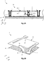
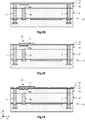
- the figure 1A is a schematic sectional view of a thermal detector described in the application WO2003 / 002963 .
- the absorbent membrane 20 is suspended above the substrate 10 by anchoring pillars 3 and thermal insulation arms (not represented). It is adapted to deform under the effect of heating until it comes into contact with the substrate 10. This contact causes the cooling of the absorbent membrane 20, thus making it possible to avoid the temperature of the absorbent membrane 20 n ' reaches a value from which a degradation of the properties of the thermometric transducer can take place.
- the absorbent membrane 20 has two parts 20.1 and 20.2 superimposed and produced so that the part 20.1 has a coefficient of thermal expansion different from that of the part 20.2. Furthermore, the absorbent membrane 20 has a protuberance 20.3 arranged projecting with respect to the plane XY of the absorbent membrane 20 and oriented towards the substrate 10. In addition, the substrate 10 comprises a contact pad 18 extending along the Z axis. Also, when the absorbent membrane 20 has excessive heating, the two superimposed parts 20.1 and 20.2 expand differently (bimetallic strip effect), which causes deformation of the absorbent membrane 20 and therefore a decrease in the spacing between the protuberance 20.3 and the contact pad 18 until there is mechanical contact between these two elements.
- the absorbent membrane 20 is then cooled, which in turn causes the protuberance 20.3 to move away from the contact pad 18.
- a continuous movement of vertical oscillation can take place at cause of the alternation of the cooling phases in contact with the substrate 10 and of heating after loss of contact.
- the figure 1B is a schematic perspective view of the thermal detector described in the application KR101181248 .
- the absorbent membrane 20 comprises a fixed detection part 21 at the level of which a thermistor material is arranged, and a deformable part 30 of bimetallic strip type. It has a first end 31 fixed to the detection part 21 and a second opposite end 32 free, that is to say that the second end 32 is movable in displacement along the axis Z under the effect of the deformation of the deformable part 30.
- the operation is similar to that described above: during excessive heating, the deformable part 30 is deformed by the bimetallic strip effect so that the free end 32 comes into contact with the substrate 10, which causes cooling of the absorbent membrane 20.
- the object of the invention is to remedy at least in part the drawbacks of the prior art, and more particularly to propose a thermal detector having improved protection against high power electromagnetic radiation.
- thermal detector Some preferred but non-limiting aspects of this thermal detector are as follows.
- the deformable part may have a maximum clearance ⁇ p max between a first position p r of the free end for a temperature T m of the absorbent membrane less than or equal to the final martensitic temperature M f , and a second position p d, max of the free end corresponding to a temperature T m greater than or equal to the final austenitic temperature A f . It can then be positioned opposite the substrate so that a maximum distance d max separating the free end occupying the first position p r and a contact surface of the substrate on which the free end is in contact at the contact temperature T c is less than or equal to the clearance maximum ⁇ p max .
- the shape memory alloy can be a metallic alloy based on NiTi.
- the shape memory alloy can be a metallic alloy chosen from Ti 50.5 Ni 24.5 Pd 25 , Ti 85.3-x Ni x Hf 14.7 with x> 50% at, and Ti 7 Ni 11 Zr 43 Cu 39 -x Co x with x> 10% at.
- the substrate may have a contact surface on which the free end is in contact at the contact temperature T c , and in which the shape memory alloy has the shape of a longitudinal strip between the fixed end and the end free, including one face oriented towards the contact surface of the substrate having protruding patterns.
- the substrate may have a flat upper face, and may include a contact pad which extends from the upper face and has a contact surface on which the free end is in contact at the contact temperature T c .
- the substrate may have a flat upper face, and the absorbent membrane may be held above the upper face of the substrate by thermal insulation arms, and by anchoring pillars which extend substantially orthogonal to the plane. of the upper face of the substrate.
- the contact pad can be made of at least one thermally conductive material identical to that of the anchoring pillars.
- the invention relates to a device for detecting electromagnetic radiation, for example infrared or terahertz radiation.
- the detection device comprises one or more thermal detectors preferably particularly suitable for detecting infrared radiation from the LWIR ( Long Wavelength Infrared ) range, the wavelength of which is between approximately 8 ⁇ m and 14 ⁇ m.
- Each thermal detector advantageously comprises a quarter-wave interference cavity formed between an absorbent membrane and a reflector, thus making it possible to maximize the absorption of the infrared radiation to be detected by the absorbent membrane.
- the thermal detector comprises an absorbent membrane suspended above a substrate by anchoring pillars and thermally insulated therefrom by thermal insulation arms.
- the absorbent membrane comprises a fixed detection part comprising the thermometric transducer, and a deformable part of thermal short circuit, which comprises a free end intended to be in contact with the substrate when the absorbent membrane reaches a so-called contact temperature T c below a predetermined protection temperature T th .
- the contact between the deformable part and the substrate makes it possible to cool the absorbent membrane, and therefore to prevent the temperature T m of the latter from reaching or even exceeding the protection temperature T th of the thermometric transducer.
- the temperature T m the absorbent membrane is an average temperature of the different parts of the absorbent membrane. It is assumed to be homogeneous, at first order, within the absorbent membrane, that is to say both in the fixed detection part and in the deformable part of thermal short-circuit.
- the deformable part of thermal short circuit is made of at least one shape memory alloy (SMA, for Shape Memory Alloy, in English), that is to say an alloy having a martensitic transformation.
- SMA shape memory alloy
- a martensitic transformation is a structural transition of the alloy, reversible and displacive type, depending on the temperature, between a martensitic phase (crystallographic phase at low temperature) and an austenitic phase (crystallographic phase at high temperature).
- the martensitic transformation has characteristic temperatures (at zero stress) which depend on the direction of the transformation.
- M s for Martensite start temperature, in English
- M f for Martensite finish temperature
- a s for Austenite start temperature
- a f for Austenite finish temperature
- the martensitic transformation exhibits a temperature hysteresis between the cooling and the heating of the alloy, insofar as the temperatures M s and A f are different from each other, just as are temperatures M f and A s .
- ⁇ m the volume fraction of the martensitic phase within the shape memory alloy.
- the volume fraction ⁇ m of the martensitic phase is initially greater than or equal to 0.95, or even equal to 1.0, when the temperature T of the shape memory alloy is less than or equal to the temperature A s . It then decreases as the temperature T increases, and is less than or equal to 0.05, or even equal to o, when the temperature T is greater than or equal to the temperature A f .
- the volume fraction ⁇ m of the martensitic phase is initially less than or equal to 0.05, or even equal to o, when the temperature T of the shape memory alloy is greater than or equal to the temperature M s . It then increases as the temperature T decreases and is greater than or equal to 0.95, or even equal to 1.0, when the temperature T is less than or equal to the temperature M f .
- the deformable part has a first rest configuration in which the free end has a first position p r .
- the deformable part is not substantially deformed, and the temperature T of the deformable part is then less than or equal to the temperature A s in the case of a reverse martensitic transformation (from martensite to austenite), or is less than or equal to the temperature M f in the case of a direct martensitic transformation (from austenite to martensite).
- the deformable part when it does not have the non-deformed configuration of rest, occupies a deformed configuration in which the free end has at least a second position p d different from the position p r .
- the deformable part is deformed in the direction of the substrate, and the temperature of the deformable part is then higher than the temperature A s in the case of a reverse martensitic transformation (from martensite to austenite), or is higher at the temperature M f in the case of a direct martensitic transformation (from austenite to martensite).
- ⁇ p max the maximum clearance of the deformable part defined between a first position p r of the free end in the rest configuration of the deformable part, and a second position p d, max of the free end in the deformed configuration when the temperature T is greater than or equal to the temperature A f .
- the positions p r and p d , max are defined along an axis Z orthogonal to the plane of the substrate. In the rest configuration, that is to say in the absence of excessive heating of the absorbent membrane, the free end of the deformable part is then spaced from the substrate by a maximum value d max less than or equal at maximum travel ⁇ p max .
- the shape memory alloy of the deformable part has an initial austenitic temperature A s from which its free end is deformed to come into contact with the substrate.
- the free end comes into contact with the substrate at a contact temperature T c higher than the initial austenitic temperature A s .
- the contact temperature T c can be, indifferently, lower, equal or higher than the final austenitic temperature A f .
- the shape memory alloy is advantageously adapted so as to have a dynamic time constant ⁇ t dyn associated with the deformation of the deformable part in response to cooling greater than the thermal time constant ⁇ t th associated with its cooling when the free end is in contact with the substrate.
- the cooling upon contact of the deformable part with the substrate causes a sudden decrease in the temperature of the shape memory alloy with the thermal time constant ⁇ t th .
- the shape memory alloy then deforms, in response to this cooling phase, with the dynamic time constant ⁇ t dyn . Insofar as ⁇ t dyn is greater than ⁇ t th , the shape memory alloy cools down to at least the temperature M f .
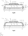
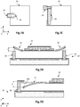
- FIGS. 3A to 3C are schematic perspective views ( fig.3A ), and in section along the plane AA ( fig. 3B and 3C ), a detection device according to one embodiment.
- a single thermal detector 1 is shown here, but the detection device advantageously comprises a matrix of identical thermal detectors (sensitive pixels).
- a direct three-dimensional orthogonal coordinate system (X, Y, Z), where the plane (X, Y) is substantially parallel to the main plane of the reading substrate of the thermal detector 1, and where the Z axis is oriented in one direction substantially orthogonal to the main plane of the reading substrate and oriented towards the absorbent membrane 20.
- the terms “lower” and “upper” are understood to relate to an increasing positioning when moving away from the reading substrate in direction + Z.
- the thermal detector 1 comprises an advantageously functionalized substrate 10, called the reading substrate, produced in this example based on silicon, comprising a reading circuit allowing the control and the reading of the thermal detectors.
- the read circuit is here in the form of a CMOS integrated circuit located in a support substrate 11. It comprises portions of conductive lines, for example metallic, separated from each other by a dielectric material, for example an inorganic material based on silicon such as a silicon oxide SiO x , a silicon nitride SiN x , or their alloys.
- the thermal detector 1 may also include active electronic elements (not shown), for example diodes, transistors, or passive electronic elements, for example capacitors, resistors, etc., connected by electrical interconnections to the thermal detector 1 on the one hand, and on the other hand to a connection pad (not shown), the latter being intended to connect the detection device 1 to an external electronic device.
- the conductive portions and the conductive vias can be made, for example, of copper, aluminum or tungsten.
- the copper or tungsten may optionally be located between sublayers made of titanium nitride, tantalum or the like.
- the reading substrate 10 here has an upper face formed in particular by a surface of an inter-metal insulating layer and a surface of conductive portions of the last level of electrical interconnection.
- This stack 10 comprises the support substrate 11, and advantageously the reflector 2 and the protective layer 17. It can also include a contact pad 18, as described in detail below, in which case the contact pad 18 is in thermal contact with the support substrate 11.
- the deformable part 30 is intended to come into contact with the stack 10, for example in contact with the contact pad 18 of the stack 10.
- the thermal detector 1 comprises a reflector 2, made of at least one material reflecting with respect to the electromagnetic radiation to be detected. It is advantageously formed here of a portion of the conductive line of the last level of electrical interconnection of the CMOS integrated circuit.
- the substrate here comprises two contact pads 18, which rest on conductive portions 15 of the last level of electrical interconnection, and are intended to form a contact surface 18a for the deformable parts 30 of the absorbent membrane 20. These contact pads 18 extend along the axis Z from the upper face 10a of the substrate 10, and are made of at least one thermally conductive material, for example a metallic material, of so that the support substrate 11 and the contact pads 18 have a substantially identical temperature.
- Each contact pad 18 is intended to be located opposite, that is to say perpendicular to a deformable part 30, so that the free end 32 thereof can come into contact with the contact pad 18.
- the substrate 10 (or stack 10) has an upper face 10a as well as a contact surface 18a. Also, when there is contact between the free end 32 of the deformable part 30 and the substrate 10, there is contact at the level of the upper face 10a or of the contact surface 18a.
- the upper face 10a is advantageously coated with a protective layer 17, in particular when the thermal detector 1 is produced by the use of mineral sacrificial layers then eliminated by chemical attack in HF acid medium (hydrofluoric acid).
- the protective layer 17 then has an etching stop function, and is therefore suitable for ensuring protection of the support substrate 11 and of the inter-metal dielectric layers when they are made of an inorganic material with respect to the HF chemical attack.
- This protective layer 17 thus forms a hermetic and chemically inert layer. It is electrically insulating to avoid any short circuit between the metal line portions. It can thus be produced in alumina Al 2 O 3 , or even in aluminum nitride or fluoride, or even in intrinsic amorphous silicon. It may have a thickness between a few tens and a few hundred nanometers, for example between 10nm and 500nm, preferably between 20nm and 100nm.
- the thermal detector 1 can have lateral dimensions in the XY plane (say not pixel), of the order of one to a few tens of microns, for example equal to about 10 ⁇ m or even less. It comprises a membrane 20 absorbing electromagnetic radiation, suspended above the reading substrate 10 by anchoring pillars 3 and connected to the reading circuit by the latter. It is also thermally insulated from the reading substrate by thermal insulation arms 4 which extend between the anchoring pillars and the absorbent membrane 20.
- the anchoring pillars 3 are conductive pads made of at least one electrically conductive material, which extend along the axis Z from the reading substrate 10 to the absorbent membrane 20. They are in contact with the portions of conductive lines, and thus ensure the electrical connection of the absorbent membrane 20 to the reading circuit.
- the anchoring pillars 3 can be made, for example, of copper, aluminum or tungsten, optionally encapsulated in at least one protective sublayer of titanium nitride, or the like.
- the thermal insulation arms 4 extend here in a substantially coplanar manner with the absorbent membrane 20, and are here formed of an electrically conductive layer allowing the electrical connection of the membrane absorbent 20 to the reading circuit, advantageously encapsulated in two lower and upper dielectric layers which help to stiffen the thermal insulation arms 4.
- the absorbent membrane 20 comprises a detection part 21 and a deformable part 30 of thermal short-circuit.
- the detection part 21 is said to be fixed in so far as it is located at a substantially constant distance from the substrate 10. It comprises an absorber formed here by the polarization electrodes 24 and a thermometric transducer.
- a thermometric transducer is an element having an electrical property varying with its heating, and can be as here a thermistor material 26 formed for example of vanadium or titanium oxide, or amorphous silicon, or in a variant can be a capacitor formed by a pyroelectric or ferroelectric material, a diode (pn or pin junction), even a field effect transistor and with metal - oxide - semiconductor structure (MOSFET).
- the detection part 21 of the absorbent membrane 20 is spaced from the reading substrate 10, and in particular from the reflector 2, by a non-zero distance. This distance is preferably adjusted so as to form a quarter-wave interference cavity optimizing the absorption of the electromagnetic radiation to be detected by the absorbent membrane 20.
- the absorbent membrane 20 is spaced from the reading substrate 10, and more precisely from the reflector 2 , from a distance typically between 1 ⁇ m and 5 ⁇ m, preferably 2 ⁇ m, when the thermal detector 1 is designed for the detection of infrared radiation included in the LWIR.
- the absorbent membrane 20 is here conventionally formed, in the detection part 21, of a stack of a lower dielectric layer 22 made of a dielectric material, of two electrodes 24 electrically isolated from one another by lateral spacing , an intermediate insulating layer 25 made of a dielectric material and covering the electrodes 24 and the lateral spacing, except in two openings opening onto the electrodes, of a thermistor material 26 such as amorphous silicon or a vanadium oxide or titanium.
- the thermistor material 26 is in contact with the two bias electrodes 24 via the openings.
- An upper protective layer 27 covers the thermistor material 26, in particular to protect the thermistor material 26 during the chemical attack with hydrofluoric acid implemented subsequently.
- the absorber is here formed by the bias electrodes 24, which are made of at least one metallic material, for example titanium nitride.
- the absorbent membrane 20 also comprises a deformable part 30 making it possible to ensure a thermal short circuit between the absorbent membrane 20 and the substrate 10 before the temperature T m of the absorbent membrane 20 reaches or exceeds the predetermined protection temperature T th of the thermistor material 26.
- the deformable part 30 is here produced in a strip having two opposite longitudinal ends: a first end fixed 31 assembled to the detection part 21, and a second end 32 known as free, that is to say capable of moving along the axis Z.
- stripe is meant a portion of material having a surface defined by a length greater than its width and a thickness less than the width.
- the temperature within the absorbent membrane 20, that is to say within the detection and thermal short-circuit parts is first order homogeneous.
- the deformable part 30 is adapted to present the first so-called rest configuration for which the temperature T m of the absorbent membrane 20 is in particular equal to a nominal temperature T n when the thermal detector 1 is not subjected to strong electromagnetic radiation power.
- the free end 32 then occupies the first position p r and its spacing d (here the maximum spacing d max ) with the upper surface 18a of the contact pad 18 is less than or equal to the maximum clearance ⁇ p max .
- the deformable part 30 is also adapted to have a second configuration known as a thermal short-circuit in which the free end 32 is in contact with the substrate 10, and here the upper surface 18a of the contact pad 18.
- the temperature T m of the absorbent membrane 20 then corresponds to the contact temperature T c at the time of mechanical contact with the substrate 10, then decreases in a cooling phase.
- the free end 32 then occupies a position p c and its spacing d with the upper surface 18a of the contact pad 18 is zero.
- the deformable part 30 is made of at least one shape memory alloy. More specifically, the shape memory alloy is a metal alloy chosen from NiTi-based alloys, copper-based Cu, or iron-based Fe. The metal alloy is chosen so that the final austenitic temperature A f is less than or equal to the predetermined temperature T th for protecting the thermometric transducer. This protection temperature depends on the type of thermometric transducer, and can be of the order of 100 ° C to 350 ° C, for example at 200 ° C.
- the metal alloy can be produced in a binary compound NiTi with an atomic proportion of nickel and titanium equal or not, or in a ternary compound NiTiA where the additional chemical element A can be iron Fe, copper Cu, zirconium Zr, hafnium Hf, platinum Pt, palladium Pd, tungsten W, gold Au, or the like. It can thus be Ti 51 Ni 38 Cu 11 where the indices represent the atomic proportion of each chemical element within the alloy.
- the thickness of the alloy in shape memory can be between a few tens of nanometers to a few hundred nanometers, for example 100 nm.
- the strip of the deformable part 30 may have a length of several microns, for example equal to between 1 and 2 ⁇ m and a width equal to a few hundred nanometers or a few microns, for example equal between 50 nm and 2 ⁇ m.
- the deformable part can thus be a strip formed continuously from at least one material based on a shape memory alloy, or be formed of nanowires based on shape memory alloy, for example having a width of a few tens of nanometers, for example 50nm.
- a deformable part with nanowires makes it possible to further reduce the heat capacity of the absorbent membrane and to obtain a greater maximum travel ⁇ p max .
- the shape memory alloy of the deformable part 30 advantageously comprises a plurality of protruding patterns (cf. fig. 6J ) and oriented towards the contact surface 18a of the substrate 10. These patterns are protuberances which extend orthogonal to the strip formed by the deformable part 30. They make it possible to obtain a deformation of the deformable part almost systematically. 30 towards the contact surface. These protruding patterns may have a height, for example of the order of a few tens of nanometers.
- the deformable part 30 is positioned with respect to the contact surface 18a of the substrate 10 (here the upper surface of the contact pad 18) so that it deforms from the initial austenitic temperature A s and touches the contact surface 18a at the contact temperature T c , this being indifferently lower, equal, or higher than the final austenitic temperature A f . Also, the contact between the free end 32 of the deformable part 30 and the contact surface 18a of the substrate 10 results in cooling of the absorbent membrane 20 and therefore a decrease in the temperature T m .
- the free end 32 of the deformable part 30 remains in contact with the contact surface 18a of the substrate 10 as long as the temperature T m remains above initial martensitic temperature M s .
- the shape memory alloy of the deformable part advantageously has a low hysteresis, that is to say a slight difference between the temperatures M s and A f , for example less than or equal to 20 ° C.
- the shape memory alloy is then preferably chosen from alloys based on TiNiPd, TiNiCuAlMn, TiNiMn).
- the contact surface 18a of the substrate 10 is the upper surface of the contact pads 18 each located opposite a deformable part 30. It can also be an area of the protective layer 17 if necessary, or a area of the upper face 10a of the substrate 10.
- the maximum spacing d max between the free end 32 in the rest configuration and the contact surface 18a of the substrate 10 is chosen so as to be less or equal to the maximum travel ⁇ p max of the shape memory alloy.
- the vertical dimensioning of the contact pad 18 makes it possible to ensure that the mechanical and therefore thermal contact between the free end 32 of the deformable part 30 on the contact pad 18 is actually carried out at a higher contact temperature T c at the initial austenitic temperature A s .
- a thermal detector 1 according to the prior art described above, the deformable part of which is of the bimetallic strip type, has a continuous movement of vertical oscillation due to the alternation of the cooling phases in contact with the substrate and of heating after loss of contact.
- This continuous vertical oscillation movement is characterized in particular by short-term mechanical contacts between the free end 32 and the contact surface 18a of the substrate 10, as well as by a low amplitude of oscillation.
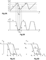
- the temperature T m is substantially equal to the nominal temperature T n . Then, a phase 1 of heating of the absorbent membrane 20 takes place from the moment when it is subjected to high power electromagnetic radiation.
- the temperature T m increases continuously (increase here rectilinear in a purely illustrative manner), and the deformable part 30 then deforms as a result, so that the spacing d between the free end 32 and the substrate 10 decreases continuously from the maximum spacing value d max , up to a zero value.
- the spacing d is then zero and the temperature T m corresponds to the contact temperature T c .
- the thermal detector 1 being always subjected to high power electromagnetic radiation, and the thermal contact with the substrate being broken, the temperature T m of the membrane increases again. This new heating phase is then noted “3” in the figures.
- the quality of the thermal contact between the deformable part 30 and the substrate is poor insofar as the mechanical contacts are of very short duration. Furthermore, this can result in an inhomogeneity of the thermal management of the various thermal detectors within the same matrix of sensitive pixels. These different aspects can lead to a deterioration in the performance of the detection device.
- the thermal detector 1 the absorbent membrane 20 of which comprises a deformable part 30 with shape memory alloy does not exhibit such a continuous movement of vertical oscillation.
- the mechanical contact between the deformable part 30 and the substrate is of greater duration and the amplitude of the vertical movement of the deformable part 30 is greater, thereby improving the quality of the thermal contact and therefore of the cooling of the absorbent membrane 20, this which contributes to preserving the performance of the detection device.
- the temperature T m of the absorbent membrane 20 initially has a nominal temperature T n in the absence of high power electromagnetic radiation. When this radiation is present (phase 1 of heating), the temperature T m of the absorbent membrane 20 increases continuously. As long as it is lower than the initial austenitic temperature A s , the deformable part 30 does not deform and the spacing d remains equal to the maximum value d max : it is part 1a. When the temperature T m reaches and exceeds the temperature A s , the shape memory alloy progressively passes from the martensitic phase to the austenitic phase, and deforms accordingly as the temperature T m increases, resulting in a decrease progressive spacing d: part 1b.
- the temperature T m increases (and the spacing d decreases) until the free end 32 touches the substrate. At this instant, the spacing d is then zero and the temperature T m corresponds to the contact temperature T c .
- the temperature T c is here lower than the temperature A f but as a variant, it could be greater than or equal to A f .
- the cooling (phase 2) of the absorbent membrane 20 due to the thermal contact between the deformable part 30 and the substrate does not immediately result in a loss of mechanical contact.
- the cooling phase 2 comprises a first part 2a in which the temperature T m of the deformable part 30 decreases without deforming until reaching the initial martensitic temperature M s .
- This hysteresis in temperature of the direct martensitic transformation makes it possible to keep the free end 32 in contact with the substrate over a longer period than in the example of the prior art.
- the shape memory alloy cools until it reaches, in this example, the final martensitic temperature M f insofar as the dynamic time constant ⁇ t dyn is greater than the thermal time constant ⁇ t th .
- the thermal time constant ⁇ t th corresponds to the time necessary for the shape memory alloy to pass from the contact temperature T c to a minimum temperature (here slightly lower than the final martensitic M f ) due to the cooling of the absorbent membrane 20.
- the dynamic time constant ⁇ t dyn corresponds to the time necessary for the shape memory alloy to pass from zero spacing to maximum spacing d max , due to the cooling of the membrane absorbent 20.
- this new heating phase 3 the deformable part 30 does not deform immediately as in the example of the prior art. Indeed, due to the hysteresis in temperature of the inverse martensitic transformation (martensite to austenite), this phase 3 has a part 3a in which the spacing d remains constant at the maximum value d max as long as the temperature T m n has not reached the initial austenitic temperature A s .
- the temperature T m continues to increase and the spacing d decreases until the thermal contact between the free end 32 and the substrate, at a temperature T c , here below the temperature A f ( but could be greater than or equal to A f ).
- the figure 5D illustrates a variant in which the thermal time constant ⁇ t th is greater than the dynamic time constant At dyn .
- the temperature T m decreases but does not reach the temperature M f because of the heating linked to the high power electromagnetic radiation.
- the heating phase comprises a part 3a in which the spacing d remains constant at an intermediate value d int as long as the temperature T m has not reaches the initial austenitic temperature A s .
- the temperature hysteresis of the direct martensitic transformation of the shape memory alloy makes it possible to improve the quality of the mechanical and therefore thermal contact between the deformable part 30 and the substrate.
- the free end 32 remains in contact with the substrate over a longer period of time, which improves the cooling of the absorbent membrane 20.
- the hysteresis of the martensitic transformation makes it possible to prevent a continuous vertical oscillation movement is set up with short-term mechanical contacts between the deformable part 30 and the substrate. The risks of degradation of the properties of the absorbent membrane 20 are then reduced. This increases the reliability and homogeneity of the thermal management of the various thermal detectors within the same matrix of sensitive pixels. The performance of the detection device is then improved.
- the thermal detector 1 is produced using mineral sacrificial layers intended to be subsequently removed by wet etching in an acid medium (HF vapor).
- the sacrificial layers can be made on the basis of polyimide or equivalent and be subsequently removed by dry etching, for example under O 2 plasma.
- the materials of the different protective layers are adapted to be inert to this type of dry etching, and can be chosen from AlN, Al 2 O 3 , amorphous carbon, amorphous silicon, among others.
- the reading substrate 10 is formed, formed of a support substrate 11 containing the reading circuit suitable for controlling and reading the thermal detector 1.
- the reading circuit thus comprises conductive portions 14 which are flush with the upper face 10a of the substrate reading 10, which is substantially planar.
- the conductive portions 14 and the conductive vias 16 can be made of copper, aluminum and / or tungsten, among others, for example by means of a damascene process in which trenches made in the inter-metal insulating layer are filled.
- the outcrop of the conductive portions 16 at the level of the upper face can be obtained by a chemical mechanical planarization (CMP) technique.
- CMP chemical mechanical planarization
- the reflector 2 of the thermal detector 1 is also produced.
- the reflector 2 is here formed by a portion of a conductive line of the last interconnection level, this being made of a metallic material suitable for reflecting the electromagnetic radiation to be detected. It is intended to extend opposite the absorbent membrane, and is intended to form with the absorber a quarter-wave interference cavity with respect to the electromagnetic radiation to be detected.
- a conductive portion 15 intended to provide support and better thermalization of a contact pad of the substrate 10. This contact pad is intended to ensure thermal contact between the substrate 10 and the deformable part of the absorbent membrane .
- the conductive portion 15 is here also formed of a portion of the conductive line of the last interconnection level.
- a protective layer 17 can then be deposited so as to cover the inter-metal insulating layer 13.
- This etching stop layer 17 is made of a material substantially inert to the etching agent used subsequently to remove the mineral sacrificial layers , for example in the HF vapor phase medium. It thus makes it possible to prevent the underlying mineral insulating layers from being etched during this step of removing the sacrificial layers. It can be formed from an aluminum oxide or nitride, from aluminum trifluoride, or from intrinsic amorphous silicon (not intentionally doped). It can be deposited for example by PVD (for Physical Vapor Deposition, in English) and can have a thickness of the order of ten nanometers to a few hundred nanometers.
- a part 3.1 of the anchoring pillars 3 is made, as well as the contact pad 18.
- a first sacrificial layer 41 is deposited on the substrate.
- reading 10 for example made of a mineral material such as a silicon oxide SiO x deposited by chemical vapor deposition assisted by plasma (PECVD).
- PECVD chemical vapor deposition assisted by plasma
- This mineral material is capable of being removed by wet chemical etching, in particular by chemical attack in an acid medium, the etchant preferably being hydrofluoric acid (HF) in the vapor phase.
- This mineral sacrificial layer 41 is deposited so as to extend continuously over substantially the entire surface of the reading substrate 10 and thus cover the etching stop layer 17.
- the thickness of the sacrificial layer 41 along the Z axis allows to define the height of the contact pad 18. It can be of the order of a few hundred nanometers to a few microns.
- Vertical orifices are then produced intended for the formation of the first parts 3.1 of the anchoring pillars 3 and for the formation of the contact pad 18. They are produced by photolithography and etching, and pass through the first mineral sacrificial layer 41 and the layer of protection 17, to lead to the conductive portions 14 of the reading circuit, and here on the conductive portion 15.
- the vertical orifices may have a cross section in the plane (X, Y) of square, rectangular, or circular shape, of an area substantially equal, for example, to 0.25 ⁇ m 2 .
- the first parts 3.1 of the anchoring pillars 3 are then produced as well as the contact pad 18 in the vertical orifices. They can be produced by filling the orifices with one or more electrically conductive materials.
- they may each comprise a layer of TiN deposited by PVD or MOCVD (for Metal Organic Chemical Vapor Deposition, in English) on the vertical sides of the orifices, and a copper or tungsten core filling the defined space. transversely through the TiN layer.
- a CMP step then makes it possible to remove the excess filling materials and to planarize the upper face formed by the sacrificial layer 41, the first parts 3.1 of the anchoring pillars 3 and the contact pad 18.
- the formation of the anchoring pillars 3 is finalized.
- a second sacrificial layer 42 is deposited on the sacrificial layer 41, for example made of an inorganic material identical to that of the sacrificial layer 41.
- Vertical orifices are then produced intended for the formation of the second parts 3.2 of the anchor pillars 3. These vertical orifices are therefore positioned so as to lead only to the first parts 3.1 of the anchor pillars 3.
- the second parts 3.2 of the anchor pillars are then produced 3 in the vertical orifices, for example produced by filling the orifices with one or more electrically conductive materials identical to those of the first parts 3.1.
- a CMP step then makes it possible to remove the excess filling materials and to planarize the upper face formed by the sacrificial layer 42 and the anchoring pillars 3.
- a partial local structuring (not through) of the sacrificial layer 42 is carried out opposite the contact pad 18, from the upper face 42a.
- This local structuring is intended to subsequently obtain a layer 33 of shape memory alloy having protruding patterns 34 oriented in the direction of the contact surface 18a of the substrate 10.
- protruding patterns 34 make it possible to obtain a deformation more systematically of the deformable part 30 in the direction of the contact surface 18 of the substrate 10.
- a lower dielectric layer 22 is deposited covering the upper face of the second sacrificial layer 42. It thus extends over the flat area of the upper face as well as in the partial local structures, without however filling them.
- the lower dielectric layer 22 can be made of amorphous silicon, silicon carbide, alumina Al 2 O 3 or aluminum nitride, among others. It may have a thickness of a few tens of nanometers, for example 20 nm, and participates in ensuring the stiffening of the thermal insulation arms.
- a layer 33 of shape memory alloy is then deposited, so as to cover the lower dielectric layer 22 and to fill the partial local structures. The layer 33 may have a thickness of a few tens to hundreds of nanometers, for example between 10 nm and 900 nm.
- the shape memory alloy can be a metallic alloy of NiTi whose atomic proportion of nickel and titanium, as well as possible additional chemical elements make it possible to obtain a final austenitic temperature A f lower than a threshold protection temperature T th .
- the shape memory alloy can thus be, for example, Ti 85.3-x Ni x Hf 14.7 with x> 50% in at.%, Ti 82-x Ni x Zr 18 with x> 49% in at.
- It can also be TiTa, TiNiPd, TiNiHf, TiNiZr, TiNiZrCuCo, CoAl, which have the advantage of having a transformation time constant (and therefore a dynamic time constant ⁇ t dyn ) susceptible to be greater than the thermal time constant ⁇ t th .
- the deformable part 30 is produced by local structuring of the layer 33 of shape memory alloy.
- a strip is obtained with a length for example of the order of 1 to 2 ⁇ m, and a width for example of between 0.3 and 2 ⁇ m.
- a first intermediate dielectric layer 23 is then deposited, for example made of a material identical to that of the lower dielectric layer 22, and with a thickness of a few tens of nanometers, so as to cover the layer lower dielectric 22 as well as the strip 33 of shape memory alloy of the deformable part 30.
- the dielectric layers 22, 23 are locally etched so as to form openings leading to the anchoring pillars 3, and a conductive layer 24 is then deposited so as to cover the intermediate dielectric layer 23 and to come into contact with the pillars d anchor 3 through the openings.
- the conductive layer 24 is therefore in contact with the upper end of the anchoring pillars 3 and is intended to ensure the electrical polarization of the thermistor material. It is made of an electrically conductive material, for example TiN with a thickness of a few nanometers to a few tens of nanometers, for example 10 nm.
- the conductive layer 24 is then locally etched so as to form a lateral spacing between two portions of the conductive layer 24 intended to form the polarization electrodes.
- a second intermediate dielectric layer 25 is then deposited so as to cover the conductive layer 24 and to come into contact with the underlying intermediate dielectric layer 23 through the lateral spacing between the two polarization electrodes 24. It is of preferably made of a dielectric material identical to that of the underlying dielectric layers and has a thickness for example of between a few tens to hundreds of nanometers.
- the intermediate dielectric layer 25 is then locally etched so as to form two openings opening onto the bias electrodes 24.
- the thermistor material 26 is then deposited, for example in amorphous silicon or in a vanadium or titanium oxide, in electrical contact with the bias electrodes 24 via the openings. It can have a thickness for example between 20nm and 200nm.
- the stack of dielectric layers 22, 23, 25, 27 and the conductive layer 24 are locally etched so as to form the thermal insulation arms as well as the absorbent membrane 20.
- the various sacrificial layers are removed so as to suspend the absorbent membrane 20 above the reading substrate.
- the suspension can be carried out after having encapsulated the thermal detector 1 in a housing (not shown) defining a vacuum cavity intended to be hermetic.
- the suspension can be obtained by chemical etching of the different mineral sacrificial layers, here by wet chemical etching by hydrofluoric acid attack in the vapor phase.
- the absorbent membrane 20 of the thermal detector 1 comprises a deformable part 30 with shape memory alloy.
- the deformable part 30 is positioned with respect to the contact surface 18a of the substrate 10 so that the maximum spacing d max is less than or equal to the maximum clearance ⁇ p max of the shape memory alloy.
- the deformable part 30 is deformed in the direction of the substrate from the temperature A s , and here the contact pad, and comes to contact the latter at a temperature T c .
- the shape memory alloy when the shape memory alloy has a dynamic time constant ⁇ t dyn greater than the thermal time constant ⁇ t th associated with the cooling of the absorbent membrane 20, the shape memory alloy passes during the cooling of the absorbent membrane 20 in response to thermal contact with the substrate, from the austenitic phase ( ⁇ m ⁇ 0.05) to the martensitic phase ( ⁇ m ⁇ 0.95), and therefore passes to a temperature less than or equal to the final martensitic temperature M f .
- the deformable part 30 may be located near a top of the absorbent membrane 20 in the XY plane, or, as here, in the center of one side of the absorbent membrane 20.
- the latter may have a notch in the XY plane in which the deformable part 30 is located, thus making it possible to reduce the filling rate ( fill factor, in English) associated with the sensitive pixel, that is to say the ratio between the surface of the absorbent membrane 20 (here with its deformable part 30) on the total surface of the sensitive pixel, in the XY plane.
- the deformable part 30 may have an upwardly curved shape (in the direction + Z) in its rest configuration (low temperature) and a substantially planar shape as shown in thermal short-circuit configuration, or even a curved shape down (in the direction -Z).
- the deformable part 30 may have a shape bent downwards (in the direction -Z) in the rest configuration, and a substantially planar shape as shown in the thermal short-circuit configuration, or even a shape bent towards the high.
- the contact pad 18 has a portion projecting in the XY plane ensuring a contact surface 18a with respect to the deformable part 30.
Landscapes
- Physics & Mathematics (AREA)
- General Physics & Mathematics (AREA)
- Spectroscopy & Molecular Physics (AREA)
- Photometry And Measurement Of Optical Pulse Characteristics (AREA)
- Fire-Detection Mechanisms (AREA)
- Lubricants (AREA)
- Thermally Actuated Switches (AREA)
Applications Claiming Priority (1)
| Application Number | Priority Date | Filing Date | Title |
|---|---|---|---|
| FR1872140A FR3089290B1 (fr) | 2018-11-30 | 2018-11-30 | Detecteur thermique a membrane suspendue comportant une partie deformable de court-circuit thermique |
Publications (1)
| Publication Number | Publication Date |
|---|---|
| EP3663733A1 true EP3663733A1 (fr) | 2020-06-10 |
Family
ID=67185084
Family Applications (1)
| Application Number | Title | Priority Date | Filing Date |
|---|---|---|---|
| EP19211794.3A Withdrawn EP3663733A1 (fr) | 2018-11-30 | 2019-11-27 | Detecteur thermique a membrane suspendue comportant une partie deformable de court-circuit thermique |
Country Status (7)
| Country | Link |
|---|---|
| US (1) | US11047738B2 (ru) |
| EP (1) | EP3663733A1 (ru) |
| KR (1) | KR20200066235A (ru) |
| CN (1) | CN111256844A (ru) |
| CA (1) | CA3062531A1 (ru) |
| FR (1) | FR3089290B1 (ru) |
| RU (1) | RU2019138079A (ru) |
Cited By (1)
| Publication number | Priority date | Publication date | Assignee | Title |
|---|---|---|---|---|
| FR3125585A1 (fr) * | 2021-07-22 | 2023-01-27 | Lynred | Micro-bolometre d’imagerie infrarouge |
Families Citing this family (1)
| Publication number | Priority date | Publication date | Assignee | Title |
|---|---|---|---|---|
| CN118258498A (zh) * | 2024-03-25 | 2024-06-28 | 安徽华创鸿度光电科技有限公司 | 一种固体激光器热沉温度监控方法及装置 |
Citations (3)
| Publication number | Priority date | Publication date | Assignee | Title |
|---|---|---|---|---|
| WO2003002963A1 (fr) | 2001-06-28 | 2003-01-09 | Commissariat A L'energie Atomique | Microbolometres et son procede de fabrication |
| KR101181248B1 (ko) * | 2011-07-22 | 2012-09-11 | 한국과학기술원 | 자기 보호 특성을 갖는 적외선 볼로미터 |
| US20180299329A1 (en) * | 2017-04-12 | 2018-10-18 | Raytheon Company | Thermal protection mechanisms for uncooled microbolometers |
Family Cites Families (2)
| Publication number | Priority date | Publication date | Assignee | Title |
|---|---|---|---|---|
| US6667479B2 (en) * | 2001-06-01 | 2003-12-23 | Raytheon Company | Advanced high speed, multi-level uncooled bolometer and method for fabricating same |
| KR101442811B1 (ko) * | 2013-08-09 | 2014-09-23 | 아이쓰리시스템 주식회사 | 온도변화에 따른 출력 변화를 완화시킨 볼로미터형 적외선 센서 |
-
2018
- 2018-11-30 FR FR1872140A patent/FR3089290B1/fr not_active Expired - Fee Related
-
2019
- 2019-11-22 CA CA3062531A patent/CA3062531A1/en not_active Abandoned
- 2019-11-26 RU RU2019138079A patent/RU2019138079A/ru unknown
- 2019-11-27 US US16/697,594 patent/US11047738B2/en active Active
- 2019-11-27 EP EP19211794.3A patent/EP3663733A1/fr not_active Withdrawn
- 2019-11-29 KR KR1020190156637A patent/KR20200066235A/ko unknown
- 2019-11-29 CN CN201911203969.8A patent/CN111256844A/zh active Pending
Patent Citations (3)
| Publication number | Priority date | Publication date | Assignee | Title |
|---|---|---|---|---|
| WO2003002963A1 (fr) | 2001-06-28 | 2003-01-09 | Commissariat A L'energie Atomique | Microbolometres et son procede de fabrication |
| KR101181248B1 (ko) * | 2011-07-22 | 2012-09-11 | 한국과학기술원 | 자기 보호 특성을 갖는 적외선 볼로미터 |
| US20180299329A1 (en) * | 2017-04-12 | 2018-10-18 | Raytheon Company | Thermal protection mechanisms for uncooled microbolometers |
Non-Patent Citations (2)
| Title |
|---|
| CHOUDHARY: "Shape memory alloy thin films and heterostructures for MEMS applications: A review", SENSORS AND ACTUATORS A, vol. 242, 2016, pages 162 - 181, XP055609953, DOI: 10.1016/j.sna.2016.02.026 |
| NITIN CHOUDHARY ET AL: "Shape memory alloy thin films and heterostructures for MEMS applications: A review", SENSORS AND ACTUATORS A: PHYSICAL, vol. 242, 6 March 2016 (2016-03-06), NL, pages 162 - 181, XP055609953, ISSN: 0924-4247, DOI: 10.1016/j.sna.2016.02.026 * |
Cited By (1)
| Publication number | Priority date | Publication date | Assignee | Title |
|---|---|---|---|---|
| FR3125585A1 (fr) * | 2021-07-22 | 2023-01-27 | Lynred | Micro-bolometre d’imagerie infrarouge |
Also Published As
| Publication number | Publication date |
|---|---|
| KR20200066235A (ko) | 2020-06-09 |
| FR3089290B1 (fr) | 2020-11-06 |
| US20200173858A1 (en) | 2020-06-04 |
| CA3062531A1 (en) | 2020-05-30 |
| CN111256844A (zh) | 2020-06-09 |
| US11047738B2 (en) | 2021-06-29 |
| FR3089290A1 (fr) | 2020-06-05 |
| RU2019138079A (ru) | 2021-05-26 |
Similar Documents
| Publication | Publication Date | Title |
|---|---|---|
| EP3657143A1 (fr) | Detecteur thermique a membrane suspendue comportant un absorbeur deformable | |
| EP3211390B1 (fr) | Dispositif de detection de rayonnement electromagnetique a plot de connexion electrique sureleve | |
| FR3005045A1 (fr) | Structure microelectromecanique et/ou nanoelectromecanique a facteur de qualite ajustable | |
| EP2693140B1 (fr) | Procédé de limitation des variations de température d'un composant électrique | |
| EP2731908B1 (fr) | Capteur miniaturise a element chauffant et procede de fabrication associe. | |
| EP3663733A1 (fr) | Detecteur thermique a membrane suspendue comportant une partie deformable de court-circuit thermique | |
| WO2020074837A1 (fr) | Dispositif de detection d'un rayonnement electromagnetique comportant une structure tridimensionnelle suspendue | |
| FR2984010A1 (fr) | Dispositif capacitif integre ayant une valeur capacitive thermiquement variable | |
| WO2022023664A1 (fr) | Micro-bolometre d'imagerie infrarouge et procedes de realisation associes | |
| WO2012168592A1 (fr) | Convertisseur thermo-mecano-electrique | |
| EP1717830B1 (fr) | Micro-condensateur électromécanique à capacité variable et procédé de fabrication d'un tel micro-condensateur | |
| EP1692475B1 (fr) | Dispositif de mesure d energie rayonnante ameliore a deux positions | |
| EP3637071A1 (fr) | Procede de fabrication d'un dispositif de detection d'un rayonnement electromagnetique a structure d'encapsulation amelioree | |
| EP3864386B1 (fr) | Procede de fabrication d'un dispositif de detection d'un rayonnement electromagnetique comportant un element de detection suspendu | |
| EP3803299B1 (fr) | Systeme de detection a pixel sensible comportant un detecteur thermique et un dispositif de compensation | |
| FR3113126A1 (fr) | Micro-bolometre d’imagerie infrarouge et procedes de realisation associes | |
| FR3070487B1 (fr) | Detecteur de rayonnement electromagnetique | |
| FR3125585A1 (fr) | Micro-bolometre d’imagerie infrarouge | |
| WO2018202992A1 (fr) | Dispositif pyroelectrique de detection infrarouge comportant un emetteur infrarouge de modulation | |
| FR3061165B1 (fr) | Structure microelectronique a amortissement visqueux controle par maitrise de l'effet thermo-piezoresistif | |
| WO2023170353A1 (fr) | Micro-bolometre d'imagerie infrarouge |
Legal Events
| Date | Code | Title | Description |
|---|---|---|---|
| PUAI | Public reference made under article 153(3) epc to a published international application that has entered the european phase |
Free format text: ORIGINAL CODE: 0009012 |
|
| STAA | Information on the status of an ep patent application or granted ep patent |
Free format text: STATUS: REQUEST FOR EXAMINATION WAS MADE |
|
| 17P | Request for examination filed |
Effective date: 20191127 |
|
| AK | Designated contracting states |
Kind code of ref document: A1 Designated state(s): AL AT BE BG CH CY CZ DE DK EE ES FI FR GB GR HR HU IE IS IT LI LT LU LV MC MK MT NL NO PL PT RO RS SE SI SK SM TR |
|
| AX | Request for extension of the european patent |
Extension state: BA ME |
|
| GRAP | Despatch of communication of intention to grant a patent |
Free format text: ORIGINAL CODE: EPIDOSNIGR1 |
|
| STAA | Information on the status of an ep patent application or granted ep patent |
Free format text: STATUS: GRANT OF PATENT IS INTENDED |
|
| INTG | Intention to grant announced |
Effective date: 20210528 |
|
| STAA | Information on the status of an ep patent application or granted ep patent |
Free format text: STATUS: THE APPLICATION IS DEEMED TO BE WITHDRAWN |
|
| 18D | Application deemed to be withdrawn |
Effective date: 20211008 |