EP3663733A1 - Heat detector with suspended membrane comprising a deformable thermal short-circuit part - Google Patents
Heat detector with suspended membrane comprising a deformable thermal short-circuit part Download PDFInfo
- Publication number
- EP3663733A1 EP3663733A1 EP19211794.3A EP19211794A EP3663733A1 EP 3663733 A1 EP3663733 A1 EP 3663733A1 EP 19211794 A EP19211794 A EP 19211794A EP 3663733 A1 EP3663733 A1 EP 3663733A1
- Authority
- EP
- European Patent Office
- Prior art keywords
- substrate
- temperature
- contact
- free end
- absorbent membrane
- Prior art date
- Legal status (The legal status is an assumption and is not a legal conclusion. Google has not performed a legal analysis and makes no representation as to the accuracy of the status listed.)
- Withdrawn
Links
Images


Classifications
-
- G—PHYSICS
- G01—MEASURING; TESTING
- G01J—MEASUREMENT OF INTENSITY, VELOCITY, SPECTRAL CONTENT, POLARISATION, PHASE OR PULSE CHARACTERISTICS OF INFRARED, VISIBLE OR ULTRAVIOLET LIGHT; COLORIMETRY; RADIATION PYROMETRY
- G01J5/00—Radiation pyrometry, e.g. infrared or optical thermometry
- G01J5/02—Constructional details
- G01J5/04—Casings
- G01J5/046—Materials; Selection of thermal materials
-
- G—PHYSICS
- G01—MEASURING; TESTING
- G01J—MEASUREMENT OF INTENSITY, VELOCITY, SPECTRAL CONTENT, POLARISATION, PHASE OR PULSE CHARACTERISTICS OF INFRARED, VISIBLE OR ULTRAVIOLET LIGHT; COLORIMETRY; RADIATION PYROMETRY
- G01J5/00—Radiation pyrometry, e.g. infrared or optical thermometry
- G01J5/02—Constructional details
- G01J5/0225—Shape of the cavity itself or of elements contained in or suspended over the cavity
- G01J5/0245—Shape of the cavity itself or of elements contained in or suspended over the cavity for performing thermal shunt
-
- G—PHYSICS
- G01—MEASURING; TESTING
- G01J—MEASUREMENT OF INTENSITY, VELOCITY, SPECTRAL CONTENT, POLARISATION, PHASE OR PULSE CHARACTERISTICS OF INFRARED, VISIBLE OR ULTRAVIOLET LIGHT; COLORIMETRY; RADIATION PYROMETRY
- G01J5/00—Radiation pyrometry, e.g. infrared or optical thermometry
- G01J5/02—Constructional details
- G01J5/021—Probe covers for thermometers, e.g. tympanic thermometers; Containers for probe covers; Disposable probes
-
- G—PHYSICS
- G01—MEASURING; TESTING
- G01J—MEASUREMENT OF INTENSITY, VELOCITY, SPECTRAL CONTENT, POLARISATION, PHASE OR PULSE CHARACTERISTICS OF INFRARED, VISIBLE OR ULTRAVIOLET LIGHT; COLORIMETRY; RADIATION PYROMETRY
- G01J5/00—Radiation pyrometry, e.g. infrared or optical thermometry
- G01J5/02—Constructional details
- G01J5/0215—Compact construction
-
- G—PHYSICS
- G01—MEASURING; TESTING
- G01J—MEASUREMENT OF INTENSITY, VELOCITY, SPECTRAL CONTENT, POLARISATION, PHASE OR PULSE CHARACTERISTICS OF INFRARED, VISIBLE OR ULTRAVIOLET LIGHT; COLORIMETRY; RADIATION PYROMETRY
- G01J5/00—Radiation pyrometry, e.g. infrared or optical thermometry
- G01J5/10—Radiation pyrometry, e.g. infrared or optical thermometry using electric radiation detectors
- G01J5/20—Radiation pyrometry, e.g. infrared or optical thermometry using electric radiation detectors using resistors, thermistors or semiconductors sensitive to radiation, e.g. photoconductive devices
-
- G—PHYSICS
- G01—MEASURING; TESTING
- G01J—MEASUREMENT OF INTENSITY, VELOCITY, SPECTRAL CONTENT, POLARISATION, PHASE OR PULSE CHARACTERISTICS OF INFRARED, VISIBLE OR ULTRAVIOLET LIGHT; COLORIMETRY; RADIATION PYROMETRY
- G01J5/00—Radiation pyrometry, e.g. infrared or optical thermometry
- G01J5/38—Radiation pyrometry, e.g. infrared or optical thermometry using extension or expansion of solids or fluids
- G01J5/40—Radiation pyrometry, e.g. infrared or optical thermometry using extension or expansion of solids or fluids using bimaterial elements
Definitions
- the field of the invention is that of thermal detectors of electromagnetic radiation, for example infrared or terahertz, comprising an absorbent membrane suspended and thermally isolated from the substrate.
- the invention applies in particular to the field of infrared or terahertz imaging, thermography, or even the detection of people or of movement.
- the electromagnetic radiation detection devices can comprise a matrix of sensitive pixels each containing a thermal detector comprising an absorbent membrane thermally insulated from the reading substrate.
- the absorbent membrane comprises an absorber of the electromagnetic radiation to be detected associated with a thermometric transducer whose electrical property varies in intensity as a function of the heating of the transducer.
- the thermometric transducer can be a thermistor material such as vanadium oxide or amorphous silicon, among others.
- the absorbent membrane is thermally insulated from the substrate and from the reading circuit, the latter being preferably arranged in the substrate.
- the absorbent membrane is generally suspended above the substrate by anchoring pillars, and is thermally insulated therefrom by thermal insulation arms.
- anchoring pillars and thermal insulation arms also have an electrical function by ensuring the electrical connection of the absorbent membrane to the reading circuit.
- the thermal detector is liable to be subjected to high power electromagnetic radiation, such as solar radiation or laser radiation.
- the absorbent membrane being thermally insulated from the substrate, it can then undergo strong heating capable of causing a degradation of the properties of the thermometric transducer.
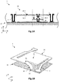
- the figure 1A is a schematic sectional view of a thermal detector described in the application WO2003 / 002963 .
- the absorbent membrane 20 is suspended above the substrate 10 by anchoring pillars 3 and thermal insulation arms (not represented). It is adapted to deform under the effect of heating until it comes into contact with the substrate 10. This contact causes the cooling of the absorbent membrane 20, thus making it possible to avoid the temperature of the absorbent membrane 20 n ' reaches a value from which a degradation of the properties of the thermometric transducer can take place.
- the absorbent membrane 20 has two parts 20.1 and 20.2 superimposed and produced so that the part 20.1 has a coefficient of thermal expansion different from that of the part 20.2. Furthermore, the absorbent membrane 20 has a protuberance 20.3 arranged projecting with respect to the plane XY of the absorbent membrane 20 and oriented towards the substrate 10. In addition, the substrate 10 comprises a contact pad 18 extending along the Z axis. Also, when the absorbent membrane 20 has excessive heating, the two superimposed parts 20.1 and 20.2 expand differently (bimetallic strip effect), which causes deformation of the absorbent membrane 20 and therefore a decrease in the spacing between the protuberance 20.3 and the contact pad 18 until there is mechanical contact between these two elements.
- the absorbent membrane 20 is then cooled, which in turn causes the protuberance 20.3 to move away from the contact pad 18.
- a continuous movement of vertical oscillation can take place at cause of the alternation of the cooling phases in contact with the substrate 10 and of heating after loss of contact.
- the figure 1B is a schematic perspective view of the thermal detector described in the application KR101181248 .
- the absorbent membrane 20 comprises a fixed detection part 21 at the level of which a thermistor material is arranged, and a deformable part 30 of bimetallic strip type. It has a first end 31 fixed to the detection part 21 and a second opposite end 32 free, that is to say that the second end 32 is movable in displacement along the axis Z under the effect of the deformation of the deformable part 30.
- the operation is similar to that described above: during excessive heating, the deformable part 30 is deformed by the bimetallic strip effect so that the free end 32 comes into contact with the substrate 10, which causes cooling of the absorbent membrane 20.
- the object of the invention is to remedy at least in part the drawbacks of the prior art, and more particularly to propose a thermal detector having improved protection against high power electromagnetic radiation.
- thermal detector Some preferred but non-limiting aspects of this thermal detector are as follows.
- the deformable part may have a maximum clearance ⁇ p max between a first position p r of the free end for a temperature T m of the absorbent membrane less than or equal to the final martensitic temperature M f , and a second position p d, max of the free end corresponding to a temperature T m greater than or equal to the final austenitic temperature A f . It can then be positioned opposite the substrate so that a maximum distance d max separating the free end occupying the first position p r and a contact surface of the substrate on which the free end is in contact at the contact temperature T c is less than or equal to the clearance maximum ⁇ p max .
- the shape memory alloy can be a metallic alloy based on NiTi.
- the shape memory alloy can be a metallic alloy chosen from Ti 50.5 Ni 24.5 Pd 25 , Ti 85.3-x Ni x Hf 14.7 with x> 50% at, and Ti 7 Ni 11 Zr 43 Cu 39 -x Co x with x> 10% at.
- the substrate may have a contact surface on which the free end is in contact at the contact temperature T c , and in which the shape memory alloy has the shape of a longitudinal strip between the fixed end and the end free, including one face oriented towards the contact surface of the substrate having protruding patterns.
- the substrate may have a flat upper face, and may include a contact pad which extends from the upper face and has a contact surface on which the free end is in contact at the contact temperature T c .
- the substrate may have a flat upper face, and the absorbent membrane may be held above the upper face of the substrate by thermal insulation arms, and by anchoring pillars which extend substantially orthogonal to the plane. of the upper face of the substrate.
- the contact pad can be made of at least one thermally conductive material identical to that of the anchoring pillars.
- the invention relates to a device for detecting electromagnetic radiation, for example infrared or terahertz radiation.
- the detection device comprises one or more thermal detectors preferably particularly suitable for detecting infrared radiation from the LWIR ( Long Wavelength Infrared ) range, the wavelength of which is between approximately 8 ⁇ m and 14 ⁇ m.
- Each thermal detector advantageously comprises a quarter-wave interference cavity formed between an absorbent membrane and a reflector, thus making it possible to maximize the absorption of the infrared radiation to be detected by the absorbent membrane.
- the thermal detector comprises an absorbent membrane suspended above a substrate by anchoring pillars and thermally insulated therefrom by thermal insulation arms.
- the absorbent membrane comprises a fixed detection part comprising the thermometric transducer, and a deformable part of thermal short circuit, which comprises a free end intended to be in contact with the substrate when the absorbent membrane reaches a so-called contact temperature T c below a predetermined protection temperature T th .
- the contact between the deformable part and the substrate makes it possible to cool the absorbent membrane, and therefore to prevent the temperature T m of the latter from reaching or even exceeding the protection temperature T th of the thermometric transducer.
- the temperature T m the absorbent membrane is an average temperature of the different parts of the absorbent membrane. It is assumed to be homogeneous, at first order, within the absorbent membrane, that is to say both in the fixed detection part and in the deformable part of thermal short-circuit.
- the deformable part of thermal short circuit is made of at least one shape memory alloy (SMA, for Shape Memory Alloy, in English), that is to say an alloy having a martensitic transformation.
- SMA shape memory alloy
- a martensitic transformation is a structural transition of the alloy, reversible and displacive type, depending on the temperature, between a martensitic phase (crystallographic phase at low temperature) and an austenitic phase (crystallographic phase at high temperature).
- the martensitic transformation has characteristic temperatures (at zero stress) which depend on the direction of the transformation.
- M s for Martensite start temperature, in English
- M f for Martensite finish temperature
- a s for Austenite start temperature
- a f for Austenite finish temperature
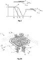
- the martensitic transformation exhibits a temperature hysteresis between the cooling and the heating of the alloy, insofar as the temperatures M s and A f are different from each other, just as are temperatures M f and A s .
- ⁇ m the volume fraction of the martensitic phase within the shape memory alloy.
- the volume fraction ⁇ m of the martensitic phase is initially greater than or equal to 0.95, or even equal to 1.0, when the temperature T of the shape memory alloy is less than or equal to the temperature A s . It then decreases as the temperature T increases, and is less than or equal to 0.05, or even equal to o, when the temperature T is greater than or equal to the temperature A f .
- the volume fraction ⁇ m of the martensitic phase is initially less than or equal to 0.05, or even equal to o, when the temperature T of the shape memory alloy is greater than or equal to the temperature M s . It then increases as the temperature T decreases and is greater than or equal to 0.95, or even equal to 1.0, when the temperature T is less than or equal to the temperature M f .
- the deformable part has a first rest configuration in which the free end has a first position p r .
- the deformable part is not substantially deformed, and the temperature T of the deformable part is then less than or equal to the temperature A s in the case of a reverse martensitic transformation (from martensite to austenite), or is less than or equal to the temperature M f in the case of a direct martensitic transformation (from austenite to martensite).
- the deformable part when it does not have the non-deformed configuration of rest, occupies a deformed configuration in which the free end has at least a second position p d different from the position p r .
- the deformable part is deformed in the direction of the substrate, and the temperature of the deformable part is then higher than the temperature A s in the case of a reverse martensitic transformation (from martensite to austenite), or is higher at the temperature M f in the case of a direct martensitic transformation (from austenite to martensite).
- ⁇ p max the maximum clearance of the deformable part defined between a first position p r of the free end in the rest configuration of the deformable part, and a second position p d, max of the free end in the deformed configuration when the temperature T is greater than or equal to the temperature A f .
- the positions p r and p d , max are defined along an axis Z orthogonal to the plane of the substrate. In the rest configuration, that is to say in the absence of excessive heating of the absorbent membrane, the free end of the deformable part is then spaced from the substrate by a maximum value d max less than or equal at maximum travel ⁇ p max .
- the shape memory alloy of the deformable part has an initial austenitic temperature A s from which its free end is deformed to come into contact with the substrate.
- the free end comes into contact with the substrate at a contact temperature T c higher than the initial austenitic temperature A s .
- the contact temperature T c can be, indifferently, lower, equal or higher than the final austenitic temperature A f .
- the shape memory alloy is advantageously adapted so as to have a dynamic time constant ⁇ t dyn associated with the deformation of the deformable part in response to cooling greater than the thermal time constant ⁇ t th associated with its cooling when the free end is in contact with the substrate.
- the cooling upon contact of the deformable part with the substrate causes a sudden decrease in the temperature of the shape memory alloy with the thermal time constant ⁇ t th .
- the shape memory alloy then deforms, in response to this cooling phase, with the dynamic time constant ⁇ t dyn . Insofar as ⁇ t dyn is greater than ⁇ t th , the shape memory alloy cools down to at least the temperature M f .
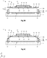
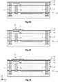
- FIGS. 3A to 3C are schematic perspective views ( fig.3A ), and in section along the plane AA ( fig. 3B and 3C ), a detection device according to one embodiment.
- a single thermal detector 1 is shown here, but the detection device advantageously comprises a matrix of identical thermal detectors (sensitive pixels).
- a direct three-dimensional orthogonal coordinate system (X, Y, Z), where the plane (X, Y) is substantially parallel to the main plane of the reading substrate of the thermal detector 1, and where the Z axis is oriented in one direction substantially orthogonal to the main plane of the reading substrate and oriented towards the absorbent membrane 20.
- the terms “lower” and “upper” are understood to relate to an increasing positioning when moving away from the reading substrate in direction + Z.
- the thermal detector 1 comprises an advantageously functionalized substrate 10, called the reading substrate, produced in this example based on silicon, comprising a reading circuit allowing the control and the reading of the thermal detectors.
- the read circuit is here in the form of a CMOS integrated circuit located in a support substrate 11. It comprises portions of conductive lines, for example metallic, separated from each other by a dielectric material, for example an inorganic material based on silicon such as a silicon oxide SiO x , a silicon nitride SiN x , or their alloys.
- the thermal detector 1 may also include active electronic elements (not shown), for example diodes, transistors, or passive electronic elements, for example capacitors, resistors, etc., connected by electrical interconnections to the thermal detector 1 on the one hand, and on the other hand to a connection pad (not shown), the latter being intended to connect the detection device 1 to an external electronic device.
- the conductive portions and the conductive vias can be made, for example, of copper, aluminum or tungsten.
- the copper or tungsten may optionally be located between sublayers made of titanium nitride, tantalum or the like.
- the reading substrate 10 here has an upper face formed in particular by a surface of an inter-metal insulating layer and a surface of conductive portions of the last level of electrical interconnection.
- This stack 10 comprises the support substrate 11, and advantageously the reflector 2 and the protective layer 17. It can also include a contact pad 18, as described in detail below, in which case the contact pad 18 is in thermal contact with the support substrate 11.
- the deformable part 30 is intended to come into contact with the stack 10, for example in contact with the contact pad 18 of the stack 10.
- the thermal detector 1 comprises a reflector 2, made of at least one material reflecting with respect to the electromagnetic radiation to be detected. It is advantageously formed here of a portion of the conductive line of the last level of electrical interconnection of the CMOS integrated circuit.
- the substrate here comprises two contact pads 18, which rest on conductive portions 15 of the last level of electrical interconnection, and are intended to form a contact surface 18a for the deformable parts 30 of the absorbent membrane 20. These contact pads 18 extend along the axis Z from the upper face 10a of the substrate 10, and are made of at least one thermally conductive material, for example a metallic material, of so that the support substrate 11 and the contact pads 18 have a substantially identical temperature.
- Each contact pad 18 is intended to be located opposite, that is to say perpendicular to a deformable part 30, so that the free end 32 thereof can come into contact with the contact pad 18.
- the substrate 10 (or stack 10) has an upper face 10a as well as a contact surface 18a. Also, when there is contact between the free end 32 of the deformable part 30 and the substrate 10, there is contact at the level of the upper face 10a or of the contact surface 18a.
- the upper face 10a is advantageously coated with a protective layer 17, in particular when the thermal detector 1 is produced by the use of mineral sacrificial layers then eliminated by chemical attack in HF acid medium (hydrofluoric acid).
- the protective layer 17 then has an etching stop function, and is therefore suitable for ensuring protection of the support substrate 11 and of the inter-metal dielectric layers when they are made of an inorganic material with respect to the HF chemical attack.
- This protective layer 17 thus forms a hermetic and chemically inert layer. It is electrically insulating to avoid any short circuit between the metal line portions. It can thus be produced in alumina Al 2 O 3 , or even in aluminum nitride or fluoride, or even in intrinsic amorphous silicon. It may have a thickness between a few tens and a few hundred nanometers, for example between 10nm and 500nm, preferably between 20nm and 100nm.
- the thermal detector 1 can have lateral dimensions in the XY plane (say not pixel), of the order of one to a few tens of microns, for example equal to about 10 ⁇ m or even less. It comprises a membrane 20 absorbing electromagnetic radiation, suspended above the reading substrate 10 by anchoring pillars 3 and connected to the reading circuit by the latter. It is also thermally insulated from the reading substrate by thermal insulation arms 4 which extend between the anchoring pillars and the absorbent membrane 20.
- the anchoring pillars 3 are conductive pads made of at least one electrically conductive material, which extend along the axis Z from the reading substrate 10 to the absorbent membrane 20. They are in contact with the portions of conductive lines, and thus ensure the electrical connection of the absorbent membrane 20 to the reading circuit.
- the anchoring pillars 3 can be made, for example, of copper, aluminum or tungsten, optionally encapsulated in at least one protective sublayer of titanium nitride, or the like.
- the thermal insulation arms 4 extend here in a substantially coplanar manner with the absorbent membrane 20, and are here formed of an electrically conductive layer allowing the electrical connection of the membrane absorbent 20 to the reading circuit, advantageously encapsulated in two lower and upper dielectric layers which help to stiffen the thermal insulation arms 4.
- the absorbent membrane 20 comprises a detection part 21 and a deformable part 30 of thermal short-circuit.
- the detection part 21 is said to be fixed in so far as it is located at a substantially constant distance from the substrate 10. It comprises an absorber formed here by the polarization electrodes 24 and a thermometric transducer.
- a thermometric transducer is an element having an electrical property varying with its heating, and can be as here a thermistor material 26 formed for example of vanadium or titanium oxide, or amorphous silicon, or in a variant can be a capacitor formed by a pyroelectric or ferroelectric material, a diode (pn or pin junction), even a field effect transistor and with metal - oxide - semiconductor structure (MOSFET).
- the detection part 21 of the absorbent membrane 20 is spaced from the reading substrate 10, and in particular from the reflector 2, by a non-zero distance. This distance is preferably adjusted so as to form a quarter-wave interference cavity optimizing the absorption of the electromagnetic radiation to be detected by the absorbent membrane 20.
- the absorbent membrane 20 is spaced from the reading substrate 10, and more precisely from the reflector 2 , from a distance typically between 1 ⁇ m and 5 ⁇ m, preferably 2 ⁇ m, when the thermal detector 1 is designed for the detection of infrared radiation included in the LWIR.
- the absorbent membrane 20 is here conventionally formed, in the detection part 21, of a stack of a lower dielectric layer 22 made of a dielectric material, of two electrodes 24 electrically isolated from one another by lateral spacing , an intermediate insulating layer 25 made of a dielectric material and covering the electrodes 24 and the lateral spacing, except in two openings opening onto the electrodes, of a thermistor material 26 such as amorphous silicon or a vanadium oxide or titanium.
- the thermistor material 26 is in contact with the two bias electrodes 24 via the openings.
- An upper protective layer 27 covers the thermistor material 26, in particular to protect the thermistor material 26 during the chemical attack with hydrofluoric acid implemented subsequently.
- the absorber is here formed by the bias electrodes 24, which are made of at least one metallic material, for example titanium nitride.
- the absorbent membrane 20 also comprises a deformable part 30 making it possible to ensure a thermal short circuit between the absorbent membrane 20 and the substrate 10 before the temperature T m of the absorbent membrane 20 reaches or exceeds the predetermined protection temperature T th of the thermistor material 26.
- the deformable part 30 is here produced in a strip having two opposite longitudinal ends: a first end fixed 31 assembled to the detection part 21, and a second end 32 known as free, that is to say capable of moving along the axis Z.
- stripe is meant a portion of material having a surface defined by a length greater than its width and a thickness less than the width.
- the temperature within the absorbent membrane 20, that is to say within the detection and thermal short-circuit parts is first order homogeneous.
- the deformable part 30 is adapted to present the first so-called rest configuration for which the temperature T m of the absorbent membrane 20 is in particular equal to a nominal temperature T n when the thermal detector 1 is not subjected to strong electromagnetic radiation power.
- the free end 32 then occupies the first position p r and its spacing d (here the maximum spacing d max ) with the upper surface 18a of the contact pad 18 is less than or equal to the maximum clearance ⁇ p max .
- the deformable part 30 is also adapted to have a second configuration known as a thermal short-circuit in which the free end 32 is in contact with the substrate 10, and here the upper surface 18a of the contact pad 18.
- the temperature T m of the absorbent membrane 20 then corresponds to the contact temperature T c at the time of mechanical contact with the substrate 10, then decreases in a cooling phase.
- the free end 32 then occupies a position p c and its spacing d with the upper surface 18a of the contact pad 18 is zero.
- the deformable part 30 is made of at least one shape memory alloy. More specifically, the shape memory alloy is a metal alloy chosen from NiTi-based alloys, copper-based Cu, or iron-based Fe. The metal alloy is chosen so that the final austenitic temperature A f is less than or equal to the predetermined temperature T th for protecting the thermometric transducer. This protection temperature depends on the type of thermometric transducer, and can be of the order of 100 ° C to 350 ° C, for example at 200 ° C.
- the metal alloy can be produced in a binary compound NiTi with an atomic proportion of nickel and titanium equal or not, or in a ternary compound NiTiA where the additional chemical element A can be iron Fe, copper Cu, zirconium Zr, hafnium Hf, platinum Pt, palladium Pd, tungsten W, gold Au, or the like. It can thus be Ti 51 Ni 38 Cu 11 where the indices represent the atomic proportion of each chemical element within the alloy.
- the thickness of the alloy in shape memory can be between a few tens of nanometers to a few hundred nanometers, for example 100 nm.
- the strip of the deformable part 30 may have a length of several microns, for example equal to between 1 and 2 ⁇ m and a width equal to a few hundred nanometers or a few microns, for example equal between 50 nm and 2 ⁇ m.
- the deformable part can thus be a strip formed continuously from at least one material based on a shape memory alloy, or be formed of nanowires based on shape memory alloy, for example having a width of a few tens of nanometers, for example 50nm.
- a deformable part with nanowires makes it possible to further reduce the heat capacity of the absorbent membrane and to obtain a greater maximum travel ⁇ p max .
- the shape memory alloy of the deformable part 30 advantageously comprises a plurality of protruding patterns (cf. fig. 6J ) and oriented towards the contact surface 18a of the substrate 10. These patterns are protuberances which extend orthogonal to the strip formed by the deformable part 30. They make it possible to obtain a deformation of the deformable part almost systematically. 30 towards the contact surface. These protruding patterns may have a height, for example of the order of a few tens of nanometers.
- the deformable part 30 is positioned with respect to the contact surface 18a of the substrate 10 (here the upper surface of the contact pad 18) so that it deforms from the initial austenitic temperature A s and touches the contact surface 18a at the contact temperature T c , this being indifferently lower, equal, or higher than the final austenitic temperature A f . Also, the contact between the free end 32 of the deformable part 30 and the contact surface 18a of the substrate 10 results in cooling of the absorbent membrane 20 and therefore a decrease in the temperature T m .
- the free end 32 of the deformable part 30 remains in contact with the contact surface 18a of the substrate 10 as long as the temperature T m remains above initial martensitic temperature M s .
- the shape memory alloy of the deformable part advantageously has a low hysteresis, that is to say a slight difference between the temperatures M s and A f , for example less than or equal to 20 ° C.
- the shape memory alloy is then preferably chosen from alloys based on TiNiPd, TiNiCuAlMn, TiNiMn).
- the contact surface 18a of the substrate 10 is the upper surface of the contact pads 18 each located opposite a deformable part 30. It can also be an area of the protective layer 17 if necessary, or a area of the upper face 10a of the substrate 10.
- the maximum spacing d max between the free end 32 in the rest configuration and the contact surface 18a of the substrate 10 is chosen so as to be less or equal to the maximum travel ⁇ p max of the shape memory alloy.
- the vertical dimensioning of the contact pad 18 makes it possible to ensure that the mechanical and therefore thermal contact between the free end 32 of the deformable part 30 on the contact pad 18 is actually carried out at a higher contact temperature T c at the initial austenitic temperature A s .
- a thermal detector 1 according to the prior art described above, the deformable part of which is of the bimetallic strip type, has a continuous movement of vertical oscillation due to the alternation of the cooling phases in contact with the substrate and of heating after loss of contact.
- This continuous vertical oscillation movement is characterized in particular by short-term mechanical contacts between the free end 32 and the contact surface 18a of the substrate 10, as well as by a low amplitude of oscillation.
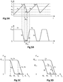
- the temperature T m is substantially equal to the nominal temperature T n . Then, a phase 1 of heating of the absorbent membrane 20 takes place from the moment when it is subjected to high power electromagnetic radiation.
- the temperature T m increases continuously (increase here rectilinear in a purely illustrative manner), and the deformable part 30 then deforms as a result, so that the spacing d between the free end 32 and the substrate 10 decreases continuously from the maximum spacing value d max , up to a zero value.
- the spacing d is then zero and the temperature T m corresponds to the contact temperature T c .
- the thermal detector 1 being always subjected to high power electromagnetic radiation, and the thermal contact with the substrate being broken, the temperature T m of the membrane increases again. This new heating phase is then noted “3” in the figures.
- the quality of the thermal contact between the deformable part 30 and the substrate is poor insofar as the mechanical contacts are of very short duration. Furthermore, this can result in an inhomogeneity of the thermal management of the various thermal detectors within the same matrix of sensitive pixels. These different aspects can lead to a deterioration in the performance of the detection device.
- the thermal detector 1 the absorbent membrane 20 of which comprises a deformable part 30 with shape memory alloy does not exhibit such a continuous movement of vertical oscillation.
- the mechanical contact between the deformable part 30 and the substrate is of greater duration and the amplitude of the vertical movement of the deformable part 30 is greater, thereby improving the quality of the thermal contact and therefore of the cooling of the absorbent membrane 20, this which contributes to preserving the performance of the detection device.
- the temperature T m of the absorbent membrane 20 initially has a nominal temperature T n in the absence of high power electromagnetic radiation. When this radiation is present (phase 1 of heating), the temperature T m of the absorbent membrane 20 increases continuously. As long as it is lower than the initial austenitic temperature A s , the deformable part 30 does not deform and the spacing d remains equal to the maximum value d max : it is part 1a. When the temperature T m reaches and exceeds the temperature A s , the shape memory alloy progressively passes from the martensitic phase to the austenitic phase, and deforms accordingly as the temperature T m increases, resulting in a decrease progressive spacing d: part 1b.
- the temperature T m increases (and the spacing d decreases) until the free end 32 touches the substrate. At this instant, the spacing d is then zero and the temperature T m corresponds to the contact temperature T c .
- the temperature T c is here lower than the temperature A f but as a variant, it could be greater than or equal to A f .
- the cooling (phase 2) of the absorbent membrane 20 due to the thermal contact between the deformable part 30 and the substrate does not immediately result in a loss of mechanical contact.
- the cooling phase 2 comprises a first part 2a in which the temperature T m of the deformable part 30 decreases without deforming until reaching the initial martensitic temperature M s .
- This hysteresis in temperature of the direct martensitic transformation makes it possible to keep the free end 32 in contact with the substrate over a longer period than in the example of the prior art.
- the shape memory alloy cools until it reaches, in this example, the final martensitic temperature M f insofar as the dynamic time constant ⁇ t dyn is greater than the thermal time constant ⁇ t th .
- the thermal time constant ⁇ t th corresponds to the time necessary for the shape memory alloy to pass from the contact temperature T c to a minimum temperature (here slightly lower than the final martensitic M f ) due to the cooling of the absorbent membrane 20.
- the dynamic time constant ⁇ t dyn corresponds to the time necessary for the shape memory alloy to pass from zero spacing to maximum spacing d max , due to the cooling of the membrane absorbent 20.
- this new heating phase 3 the deformable part 30 does not deform immediately as in the example of the prior art. Indeed, due to the hysteresis in temperature of the inverse martensitic transformation (martensite to austenite), this phase 3 has a part 3a in which the spacing d remains constant at the maximum value d max as long as the temperature T m n has not reached the initial austenitic temperature A s .
- the temperature T m continues to increase and the spacing d decreases until the thermal contact between the free end 32 and the substrate, at a temperature T c , here below the temperature A f ( but could be greater than or equal to A f ).
- the figure 5D illustrates a variant in which the thermal time constant ⁇ t th is greater than the dynamic time constant At dyn .
- the temperature T m decreases but does not reach the temperature M f because of the heating linked to the high power electromagnetic radiation.
- the heating phase comprises a part 3a in which the spacing d remains constant at an intermediate value d int as long as the temperature T m has not reaches the initial austenitic temperature A s .
- the temperature hysteresis of the direct martensitic transformation of the shape memory alloy makes it possible to improve the quality of the mechanical and therefore thermal contact between the deformable part 30 and the substrate.
- the free end 32 remains in contact with the substrate over a longer period of time, which improves the cooling of the absorbent membrane 20.
- the hysteresis of the martensitic transformation makes it possible to prevent a continuous vertical oscillation movement is set up with short-term mechanical contacts between the deformable part 30 and the substrate. The risks of degradation of the properties of the absorbent membrane 20 are then reduced. This increases the reliability and homogeneity of the thermal management of the various thermal detectors within the same matrix of sensitive pixels. The performance of the detection device is then improved.
- the thermal detector 1 is produced using mineral sacrificial layers intended to be subsequently removed by wet etching in an acid medium (HF vapor).
- the sacrificial layers can be made on the basis of polyimide or equivalent and be subsequently removed by dry etching, for example under O 2 plasma.
- the materials of the different protective layers are adapted to be inert to this type of dry etching, and can be chosen from AlN, Al 2 O 3 , amorphous carbon, amorphous silicon, among others.
- the reading substrate 10 is formed, formed of a support substrate 11 containing the reading circuit suitable for controlling and reading the thermal detector 1.
- the reading circuit thus comprises conductive portions 14 which are flush with the upper face 10a of the substrate reading 10, which is substantially planar.
- the conductive portions 14 and the conductive vias 16 can be made of copper, aluminum and / or tungsten, among others, for example by means of a damascene process in which trenches made in the inter-metal insulating layer are filled.
- the outcrop of the conductive portions 16 at the level of the upper face can be obtained by a chemical mechanical planarization (CMP) technique.
- CMP chemical mechanical planarization
- the reflector 2 of the thermal detector 1 is also produced.
- the reflector 2 is here formed by a portion of a conductive line of the last interconnection level, this being made of a metallic material suitable for reflecting the electromagnetic radiation to be detected. It is intended to extend opposite the absorbent membrane, and is intended to form with the absorber a quarter-wave interference cavity with respect to the electromagnetic radiation to be detected.
- a conductive portion 15 intended to provide support and better thermalization of a contact pad of the substrate 10. This contact pad is intended to ensure thermal contact between the substrate 10 and the deformable part of the absorbent membrane .
- the conductive portion 15 is here also formed of a portion of the conductive line of the last interconnection level.
- a protective layer 17 can then be deposited so as to cover the inter-metal insulating layer 13.
- This etching stop layer 17 is made of a material substantially inert to the etching agent used subsequently to remove the mineral sacrificial layers , for example in the HF vapor phase medium. It thus makes it possible to prevent the underlying mineral insulating layers from being etched during this step of removing the sacrificial layers. It can be formed from an aluminum oxide or nitride, from aluminum trifluoride, or from intrinsic amorphous silicon (not intentionally doped). It can be deposited for example by PVD (for Physical Vapor Deposition, in English) and can have a thickness of the order of ten nanometers to a few hundred nanometers.
- a part 3.1 of the anchoring pillars 3 is made, as well as the contact pad 18.
- a first sacrificial layer 41 is deposited on the substrate.
- reading 10 for example made of a mineral material such as a silicon oxide SiO x deposited by chemical vapor deposition assisted by plasma (PECVD).
- PECVD chemical vapor deposition assisted by plasma
- This mineral material is capable of being removed by wet chemical etching, in particular by chemical attack in an acid medium, the etchant preferably being hydrofluoric acid (HF) in the vapor phase.
- This mineral sacrificial layer 41 is deposited so as to extend continuously over substantially the entire surface of the reading substrate 10 and thus cover the etching stop layer 17.
- the thickness of the sacrificial layer 41 along the Z axis allows to define the height of the contact pad 18. It can be of the order of a few hundred nanometers to a few microns.
- Vertical orifices are then produced intended for the formation of the first parts 3.1 of the anchoring pillars 3 and for the formation of the contact pad 18. They are produced by photolithography and etching, and pass through the first mineral sacrificial layer 41 and the layer of protection 17, to lead to the conductive portions 14 of the reading circuit, and here on the conductive portion 15.
- the vertical orifices may have a cross section in the plane (X, Y) of square, rectangular, or circular shape, of an area substantially equal, for example, to 0.25 ⁇ m 2 .
- the first parts 3.1 of the anchoring pillars 3 are then produced as well as the contact pad 18 in the vertical orifices. They can be produced by filling the orifices with one or more electrically conductive materials.
- they may each comprise a layer of TiN deposited by PVD or MOCVD (for Metal Organic Chemical Vapor Deposition, in English) on the vertical sides of the orifices, and a copper or tungsten core filling the defined space. transversely through the TiN layer.
- a CMP step then makes it possible to remove the excess filling materials and to planarize the upper face formed by the sacrificial layer 41, the first parts 3.1 of the anchoring pillars 3 and the contact pad 18.
- the formation of the anchoring pillars 3 is finalized.
- a second sacrificial layer 42 is deposited on the sacrificial layer 41, for example made of an inorganic material identical to that of the sacrificial layer 41.
- Vertical orifices are then produced intended for the formation of the second parts 3.2 of the anchor pillars 3. These vertical orifices are therefore positioned so as to lead only to the first parts 3.1 of the anchor pillars 3.
- the second parts 3.2 of the anchor pillars are then produced 3 in the vertical orifices, for example produced by filling the orifices with one or more electrically conductive materials identical to those of the first parts 3.1.
- a CMP step then makes it possible to remove the excess filling materials and to planarize the upper face formed by the sacrificial layer 42 and the anchoring pillars 3.
- a partial local structuring (not through) of the sacrificial layer 42 is carried out opposite the contact pad 18, from the upper face 42a.
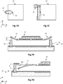
- This local structuring is intended to subsequently obtain a layer 33 of shape memory alloy having protruding patterns 34 oriented in the direction of the contact surface 18a of the substrate 10.
- protruding patterns 34 make it possible to obtain a deformation more systematically of the deformable part 30 in the direction of the contact surface 18 of the substrate 10.
- a lower dielectric layer 22 is deposited covering the upper face of the second sacrificial layer 42. It thus extends over the flat area of the upper face as well as in the partial local structures, without however filling them.
- the lower dielectric layer 22 can be made of amorphous silicon, silicon carbide, alumina Al 2 O 3 or aluminum nitride, among others. It may have a thickness of a few tens of nanometers, for example 20 nm, and participates in ensuring the stiffening of the thermal insulation arms.
- a layer 33 of shape memory alloy is then deposited, so as to cover the lower dielectric layer 22 and to fill the partial local structures. The layer 33 may have a thickness of a few tens to hundreds of nanometers, for example between 10 nm and 900 nm.
- the shape memory alloy can be a metallic alloy of NiTi whose atomic proportion of nickel and titanium, as well as possible additional chemical elements make it possible to obtain a final austenitic temperature A f lower than a threshold protection temperature T th .
- the shape memory alloy can thus be, for example, Ti 85.3-x Ni x Hf 14.7 with x> 50% in at.%, Ti 82-x Ni x Zr 18 with x> 49% in at.
- It can also be TiTa, TiNiPd, TiNiHf, TiNiZr, TiNiZrCuCo, CoAl, which have the advantage of having a transformation time constant (and therefore a dynamic time constant ⁇ t dyn ) susceptible to be greater than the thermal time constant ⁇ t th .
- the deformable part 30 is produced by local structuring of the layer 33 of shape memory alloy.
- a strip is obtained with a length for example of the order of 1 to 2 ⁇ m, and a width for example of between 0.3 and 2 ⁇ m.
- a first intermediate dielectric layer 23 is then deposited, for example made of a material identical to that of the lower dielectric layer 22, and with a thickness of a few tens of nanometers, so as to cover the layer lower dielectric 22 as well as the strip 33 of shape memory alloy of the deformable part 30.
- the dielectric layers 22, 23 are locally etched so as to form openings leading to the anchoring pillars 3, and a conductive layer 24 is then deposited so as to cover the intermediate dielectric layer 23 and to come into contact with the pillars d anchor 3 through the openings.
- the conductive layer 24 is therefore in contact with the upper end of the anchoring pillars 3 and is intended to ensure the electrical polarization of the thermistor material. It is made of an electrically conductive material, for example TiN with a thickness of a few nanometers to a few tens of nanometers, for example 10 nm.
- the conductive layer 24 is then locally etched so as to form a lateral spacing between two portions of the conductive layer 24 intended to form the polarization electrodes.
- a second intermediate dielectric layer 25 is then deposited so as to cover the conductive layer 24 and to come into contact with the underlying intermediate dielectric layer 23 through the lateral spacing between the two polarization electrodes 24. It is of preferably made of a dielectric material identical to that of the underlying dielectric layers and has a thickness for example of between a few tens to hundreds of nanometers.
- the intermediate dielectric layer 25 is then locally etched so as to form two openings opening onto the bias electrodes 24.
- the thermistor material 26 is then deposited, for example in amorphous silicon or in a vanadium or titanium oxide, in electrical contact with the bias electrodes 24 via the openings. It can have a thickness for example between 20nm and 200nm.
- the stack of dielectric layers 22, 23, 25, 27 and the conductive layer 24 are locally etched so as to form the thermal insulation arms as well as the absorbent membrane 20.
- the various sacrificial layers are removed so as to suspend the absorbent membrane 20 above the reading substrate.
- the suspension can be carried out after having encapsulated the thermal detector 1 in a housing (not shown) defining a vacuum cavity intended to be hermetic.
- the suspension can be obtained by chemical etching of the different mineral sacrificial layers, here by wet chemical etching by hydrofluoric acid attack in the vapor phase.
- the absorbent membrane 20 of the thermal detector 1 comprises a deformable part 30 with shape memory alloy.
- the deformable part 30 is positioned with respect to the contact surface 18a of the substrate 10 so that the maximum spacing d max is less than or equal to the maximum clearance ⁇ p max of the shape memory alloy.
- the deformable part 30 is deformed in the direction of the substrate from the temperature A s , and here the contact pad, and comes to contact the latter at a temperature T c .
- the shape memory alloy when the shape memory alloy has a dynamic time constant ⁇ t dyn greater than the thermal time constant ⁇ t th associated with the cooling of the absorbent membrane 20, the shape memory alloy passes during the cooling of the absorbent membrane 20 in response to thermal contact with the substrate, from the austenitic phase ( ⁇ m ⁇ 0.05) to the martensitic phase ( ⁇ m ⁇ 0.95), and therefore passes to a temperature less than or equal to the final martensitic temperature M f .
- the deformable part 30 may be located near a top of the absorbent membrane 20 in the XY plane, or, as here, in the center of one side of the absorbent membrane 20.
- the latter may have a notch in the XY plane in which the deformable part 30 is located, thus making it possible to reduce the filling rate ( fill factor, in English) associated with the sensitive pixel, that is to say the ratio between the surface of the absorbent membrane 20 (here with its deformable part 30) on the total surface of the sensitive pixel, in the XY plane.
- the deformable part 30 may have an upwardly curved shape (in the direction + Z) in its rest configuration (low temperature) and a substantially planar shape as shown in thermal short-circuit configuration, or even a curved shape down (in the direction -Z).
- the deformable part 30 may have a shape bent downwards (in the direction -Z) in the rest configuration, and a substantially planar shape as shown in the thermal short-circuit configuration, or even a shape bent towards the high.
- the contact pad 18 has a portion projecting in the XY plane ensuring a contact surface 18a with respect to the deformable part 30.
Landscapes
- Physics & Mathematics (AREA)
- General Physics & Mathematics (AREA)
- Spectroscopy & Molecular Physics (AREA)
- Photometry And Measurement Of Optical Pulse Characteristics (AREA)
- Thermally Actuated Switches (AREA)
- Lubricants (AREA)
- Fire-Detection Mechanisms (AREA)
Abstract
L'invention porte sur un détecteur thermique comportant un substrat (10), une membrane absorbante (20) comportant une partie fixe (21) et une partie déformable (30), celle-ci comportant un alliage à mémoire de forme, et étant disposée vis-à-vis du substrat de sorte que son extrémité libre (32) est au contact du substrat (10) à la température de contact T<sub>c</sub>supérieure à la température austénitique initiale A<sub>s</sub>.The invention relates to a thermal detector comprising a substrate (10), an absorbent membrane (20) comprising a fixed part (21) and a deformable part (30), the latter comprising a shape memory alloy, and being arranged vis-à-vis the substrate so that its free end (32) is in contact with the substrate (10) at the contact temperature T <sub> c </sub> higher than the initial austenitic temperature A <sub> s < / sub>.
Description
Le domaine de l'invention est celui de détecteurs thermiques d'un rayonnement électromagnétique, par exemple infrarouge ou térahertz, comportant une membrane absorbante suspendue et thermiquement isolée du substrat. L'invention s'applique notamment au domaine de l'imagerie infrarouge ou térahertz, de la thermographie, voire de la détection de personne ou de mouvement.The field of the invention is that of thermal detectors of electromagnetic radiation, for example infrared or terahertz, comprising an absorbent membrane suspended and thermally isolated from the substrate. The invention applies in particular to the field of infrared or terahertz imaging, thermography, or even the detection of people or of movement.
Les dispositifs de détection de rayonnement électromagnétique peuvent comporter une matrice de pixels sensibles contenant chacun un détecteur thermique comportant une membrane absorbante thermiquement isolée du substrat de lecture. La membrane absorbante comporte un absorbeur du rayonnement électromagnétique à détecter associé à un transducteur thermométrique dont une propriété électrique varie en intensité en fonction de l'échauffement du transducteur. Le transducteur thermométrique peut être un matériau thermistance tel qu'un oxyde de vanadium ou du silicium amorphe, entre autres.The electromagnetic radiation detection devices can comprise a matrix of sensitive pixels each containing a thermal detector comprising an absorbent membrane thermally insulated from the reading substrate. The absorbent membrane comprises an absorber of the electromagnetic radiation to be detected associated with a thermometric transducer whose electrical property varies in intensity as a function of the heating of the transducer. The thermometric transducer can be a thermistor material such as vanadium oxide or amorphous silicon, among others.
La température du transducteur thermométrique étant cependant grandement dépendante de son environnement, la membrane absorbante est isolée thermiquement du substrat et du circuit de lecture, celui-ci étant de préférence disposé dans le substrat. Ainsi, la membrane absorbante est généralement suspendue au-dessus du substrat par des piliers d'ancrage, et en est isolée thermiquement par des bras d'isolation thermique. Ces piliers d'ancrage et bras d'isolation thermique présentent également une fonction électrique en assurant la connexion électrique de la membrane absorbante au circuit de lecture.The temperature of the thermometric transducer being however largely dependent on its environment, the absorbent membrane is thermally insulated from the substrate and from the reading circuit, the latter being preferably arranged in the substrate. Thus, the absorbent membrane is generally suspended above the substrate by anchoring pillars, and is thermally insulated therefrom by thermal insulation arms. These anchoring pillars and thermal insulation arms also have an electrical function by ensuring the electrical connection of the absorbent membrane to the reading circuit.
Cependant, le détecteur thermique est susceptible d'être soumis à un rayonnement électromagnétique de forte puissance, tel qu'un rayonnement solaire ou un rayonnement laser. La membrane absorbante étant isolée thermiquement du substrat, elle peut alors subir un fort échauffement susceptible de provoquer une dégradation des propriétés du transducteur thermométrique.However, the thermal detector is liable to be subjected to high power electromagnetic radiation, such as solar radiation or laser radiation. The absorbent membrane being thermally insulated from the substrate, it can then undergo strong heating capable of causing a degradation of the properties of the thermometric transducer.
A ce titre, la
Pour cela, la membrane absorbante 20 comporte deux parties 20.1 et 20.2 superposées et réalisées de sorte que la partie 20.1 présente un coefficient de dilatation thermique différent de celui de la partie 20.2. Par ailleurs, la membrane absorbante 20 comporte une protubérance 20.3 disposée en saillie vis-à-vis du plan XY de la membrane absorbante 20 et orientée en direction du substrat 10. De plus, le substrat 10 comporte un plot de contact 18 s'étendant suivant l'axe Z. Aussi, lorsque la membrane absorbante 20 présente un échauffement excessif, les deux parties superposées 20.1 et 20.2 se dilatent de manière différente (effet bilame), ce qui provoque une déformation de la membrane absorbante 20 et donc une diminution de l'espacement entre la protubérance 20.3 et le plot de contact 18 jusqu'à ce qu'il y ait contact mécanique entre ces deux éléments. La membrane absorbante 20 est alors refroidie, ce qui provoque en retour l'écartement de la protubérance 20.3 vis-à-vis du plot de contact 18. Cependant, il apparaît qu'un mouvement continu d'oscillation verticale peut se mettre en place à cause de l'alternance des phases de refroidissement au contact du substrat 10 et de réchauffement après perte du contact.For this, the
La
L'invention a pour objectif de remédier au moins en partie aux inconvénients de l'art antérieur, et plus particulièrement de proposer un détecteur thermique présentant une protection améliorée vis-à-vis des rayonnements électromagnétiques de forte puissance.The object of the invention is to remedy at least in part the drawbacks of the prior art, and more particularly to propose a thermal detector having improved protection against high power electromagnetic radiation.
Pour cela, l'objet de l'invention est un détecteur thermique adapté à détecter un rayonnement électromagnétique, comportant :
- ∘ un substrat ;
- ∘ une membrane absorbante du rayonnement électromagnétique, thermiquement isolée vis-à-vis du substrat, et comportant :
- ▪ une partie fixe dite de détection comportant un transducteur thermométrique,
- ▪ une partie déformable dite de court-circuit thermique,
- comportant une extrémité fixe assemblée à la partie fixe de détection, et une extrémité libre opposée,
- adaptée à se déformer sous l'effet d'une variation de température de la membrane absorbante, de sorte que l'extrémité libre de la partie déformable vienne au contact du substrat à une température dite de contact Tc de la membrane absorbante.
- ∘ a substrate;
- ∘ a membrane absorbing electromagnetic radiation, thermally insulated from the substrate, and comprising:
- ▪ a fixed so-called detection part comprising a thermometric transducer,
- ▪ a deformable part called a thermal short-circuit,
- comprising a fixed end assembled to the fixed detection part, and an opposite free end,
- adapted to deform under the effect of a temperature variation of the absorbent membrane, so that the free end of the deformable part comes into contact with the substrate at a so-called contact temperature T c of the absorbent membrane.
Selon l'invention, la partie déformable :
- ▪ comporte un alliage à mémoire de forme présentant une transformation martensitique dite inverse d'une phase martensitique en une phase austénitique dudit alliage entre des températures dites austénitiques initiale As et finale Af, et une transformation martensitique dite directe de la phase austénitique en la phase martensitique entre des températures dites martensitiques initiale Ms et finale Mf, la température austénitique finale Af étant supérieure à la température martensitique initiale Ms, et
- ▪ est disposée vis-à-vis du substrat de sorte que l'extrémité libre est au contact du substrat à la température de contact Tc supérieure à la température austénitique initiale As.
- ▪ comprises a shape memory alloy having a so-called reverse martensitic transformation of a martensitic phase into an austenitic phase of said alloy between so-called initial austenitic temperatures A s and final A f , and a so-called direct martensitic transformation of the austenitic phase into martensitic phase between so-called initial martensitic temperatures M s and final M f , the final austenitic temperature A f being greater than the initial martensitic temperature M s , and
- ▪ is arranged with respect to the substrate so that the free end is in contact with the substrate at the contact temperature T c higher than the initial austenitic temperature A s .
Certains aspects préférés mais non limitatifs de ce détecteur thermique sont les suivants.Some preferred but non-limiting aspects of this thermal detector are as follows.
La partie déformable peut présenter un débattement maximal Δpmax entre une première position pr de l'extrémité libre pour une température Tm de la membrane absorbante inférieure ou égale à la température martensitique finale Mf, et une deuxième position pd,max de l'extrémité libre correspondant à une température Tm supérieure ou égale à la température austénitique finale Af. Elle peut alors être positionnée vis-à-vis du substrat de sorte qu'une distance maximale dmax séparant l'extrémité libre occupant la première position pr et une surface de contact du substrat sur laquelle l'extrémité libre est au contact à la température de contact Tc est inférieure ou égale au débattement maximal Δpmax.The deformable part may have a maximum clearance Δp max between a first position p r of the free end for a temperature T m of the absorbent membrane less than or equal to the final martensitic temperature M f , and a second position p d, max of the free end corresponding to a temperature T m greater than or equal to the final austenitic temperature A f . It can then be positioned opposite the substrate so that a maximum distance d max separating the free end occupying the first position p r and a contact surface of the substrate on which the free end is in contact at the contact temperature T c is less than or equal to the clearance maximum Δp max .
L'alliage à mémoire de forme peut être un alliage métallique à base de NiTi.The shape memory alloy can be a metallic alloy based on NiTi.
L'alliage à mémoire de forme peut être un alliage métallique choisi parmi le Ti50,5Ni24.5Pd25, le Ti85.3-xNixHf14.7 avec x>50%at, et le Ti7Ni11Zr43Cu39-xCox avec x>10%at.The shape memory alloy can be a metallic alloy chosen from Ti 50.5 Ni 24.5 Pd 25 , Ti 85.3-x Ni x Hf 14.7 with x> 50% at, and Ti 7 Ni 11 Zr 43 Cu 39 -x Co x with x> 10% at.
Le substrat peut présenter une surface de contact sur laquelle l'extrémité libre est au contact à la température de contact Tc, et dans lequel l'alliage à mémoire de forme présente une forme de bande longitudinale entre l'extrémité fixe et l'extrémité libre, dont une face orientée vers la surface de contact du substrat présentant des motifs en saillie.The substrate may have a contact surface on which the free end is in contact at the contact temperature T c , and in which the shape memory alloy has the shape of a longitudinal strip between the fixed end and the end free, including one face oriented towards the contact surface of the substrate having protruding patterns.
Le substrat peut présenter une face supérieure plane, et peut comporter un plot de contact qui s'étend à partir de la face supérieure et présente une surface de contact sur laquelle l'extrémité libre est au contact à la température de contact Tc.The substrate may have a flat upper face, and may include a contact pad which extends from the upper face and has a contact surface on which the free end is in contact at the contact temperature T c .
Le substrat peut présenter une face supérieure plane, et la membrane absorbante peut être maintenue au-dessus de la face supérieure du substrat par des bras d'isolation thermique, et par des piliers d'ancrage qui s'étendent de manière sensiblement orthogonale au plan de la face supérieure du substrat.The substrate may have a flat upper face, and the absorbent membrane may be held above the upper face of the substrate by thermal insulation arms, and by anchoring pillars which extend substantially orthogonal to the plane. of the upper face of the substrate.
Le plot de contact peut être réalisé en au moins un matériau thermiquement conducteur identique à celui des piliers d'ancrage.The contact pad can be made of at least one thermally conductive material identical to that of the anchoring pillars.
L'invention porte également sur un procédé de fabrication du détecteur thermique selon l'une quelconque des caractéristiques précédentes, comportant les étapes suivantes :
- fourniture d'un substrat présentant une surface dite de contact ;
- dépôt d'au moins une couche sacrificielle ;
- réalisation de piliers d'ancrage au travers de la couche sacrificielle ;
- réalisation de bras d'isolation thermique et d'une membrane absorbante sur la couche sacrificielle, la membrane absorbante comportant une partie déformable située en regard de la surface de contact ;
- suppression de la couche sacrificielle.
- providing a substrate having a so-called contact surface;
- depositing at least one sacrificial layer;
- realization of anchoring pillars through the sacrificial layer;
- production of thermal insulation arms and an absorbent membrane on the sacrificial layer, the absorbent membrane comprising a deformable part situated opposite the contact surface;
- removal of the sacrificial layer.
D'autres aspects, buts, avantages et caractéristiques de l'invention apparaîtront mieux à la lecture de la description détaillée suivante de formes de réalisation préférées de celle-ci, donnée à titre d'exemple non limitatif, et faite en référence aux dessins annexés sur lesquels :
- les
figures 1A et 1B , déjà décrites, sont des vues schématiques, en coupe (fig.iA) et en perspective (fig.1B ), d'un détecteur thermique selon deux exemples de l'art antérieur ; - la
figure 2 est un graphe qui illustre l'évolution en température de la fraction volumique χm de la phase martensitique au sein d'un alliage à mémoire de forme, ainsi que la déformation d'une partie déformable d'une membrane absorbante ; - les
figures 3A à 3C sont des vues schématiques, en perspective (fig.3A ) et en coupe (fig.3B et fig.3C ), d'un dispositif de détection selon un mode de réalisation ; - les
figures 4A à 4C sont des graphes qui illustrent, dans le cas du détecteur thermique de l'art antérieur illustré sur la fig.iB, des exemples :- d'une évolution temporelle de la température Tm de la membrane absorbante (
fig.4A ), - d'une évolution temporelle de l'espacement d de la partie déformable vis-à-vis du substrat (
fig.4B ), et - d'une évolution en température de l'espacement d de la partie déformable (
fig.4C ) ;
- d'une évolution temporelle de la température Tm de la membrane absorbante (
- les
figures 5A à 5D sont des graphes qui illustrent, dans le cas du détecteur thermique selon le mode de réalisation illustré sur lesfig.3A à 3C , des exemples :- d'une évolution temporelle de la température Tm de la membrane absorbante (
fig.5A ), - d'une évolution temporelle de l'espacement d de la partie déformable vis-à-vis du substrat (
fig.5B ), et - d'évolutions en température de l'espacement d de la partie déformable (
fig.5C et 5D ) ;
- d'une évolution temporelle de la température Tm de la membrane absorbante (
- les
figures 6A à 6J illustrent différentes étapes d'un procédé de fabrication du dispositif de détection selon le mode de réalisation illustré sur lesfig.3A à 3C ; - les
figures 7A à 7D sont des vues schématiques en coupe/de dessus de différents détecteurs thermiques selon des variantes de réalisation.
- the
Figures 1A and 1B , already described, are schematic views, in section (fig.iA) and in perspective (fig. 1B ), a thermal detector according to two examples of the prior art; - the
figure 2 is a graph which illustrates the evolution in temperature of the volume fraction χ m of the martensitic phase within a shape memory alloy, as well as the deformation of a deformable part of an absorbent membrane; - the
Figures 3A to 3C are schematic perspective views (fig.3A ) and in section (fig.3B and fig.3C ), of a detection device according to one embodiment; - the
Figures 4A to 4C are graphs which illustrate, in the case of the thermal detector of the prior art illustrated in FIG. iB, examples:- a temporal evolution of the temperature T m of the absorbent membrane (
fig. 4A ), - of a temporal evolution of the spacing d of the deformable part with respect to the substrate (
fig.4B ), and - of a change in temperature of the spacing d of the deformable part (
fig. 4C );
- a temporal evolution of the temperature T m of the absorbent membrane (
- the
Figures 5A to 5D are graphs which illustrate, in the case of the thermal detector according to the embodiment illustrated in thefig. 3A to 3C , examples :- a temporal evolution of the temperature T m of the absorbent membrane (
fig.5A ), - of a temporal evolution of the spacing d of the deformable part with respect to the substrate (
fig.5B ), and - changes in temperature of the spacing d of the deformable part (
fig. 5C and 5D );
- a temporal evolution of the temperature T m of the absorbent membrane (
- the
Figures 6A to 6J illustrate different stages of a method of manufacturing the detection device according to the embodiment illustrated in thefig. 3A to 3C ; - the
Figures 7A to 7D are schematic sectional / top views of different thermal detectors according to alternative embodiments.
Sur les figures et dans la suite de la description, les mêmes références représentent les éléments identiques ou similaires. De plus, les différents éléments ne sont pas représentés à l'échelle de manière à privilégier la clarté des figures. Par ailleurs, les différents modes de réalisation et variantes ne sont pas exclusifs les uns des autres et peuvent être combinés entre eux. Sauf indication contraire, les termes « sensiblement », « environ », « de l'ordre de » signifient à 10% près, et de préférence à 5% près. Par ailleurs, l'expression « comportant un » doit être comprise, sauf indication contraire, comme « comportant au moins un » et non pas comme « comportant un unique ».In the figures and in the following description, the same references represent the same or similar elements. In addition, the different elements are not shown to scale so as to favor the clarity of the figures. Furthermore, the different embodiments and variants are not mutually exclusive and can be combined with one another. Unless otherwise indicated, the terms "substantially", "approximately", "of the order of" mean to the nearest 10%, and preferably to the nearest 5%. By elsewhere, the expression "comprising a" should be understood, unless otherwise indicated, as "comprising at least one" and not as "comprising a single".
L'invention porte sur un dispositif de détection d'un rayonnement électromagnétique, par exemple un rayonnement infrarouge ou térahertz. Le dispositif de détection comporte un ou plusieurs détecteurs thermiques de préférence particulièrement adaptés à détecter un rayonnement infrarouge de la gamme LWIR (Long Wavelength Infrared, en anglais) dont la longueur d'onde est comprise entre 8µm et 14µm environ. Chaque détecteur thermique comporte avantageusement une cavité interférentielle quart d'onde formée entre une membrane absorbante et un réflecteur, permettant ainsi de maximiser l'absorption du rayonnement infrarouge à détecter par la membrane absorbante.The invention relates to a device for detecting electromagnetic radiation, for example infrared or terahertz radiation. The detection device comprises one or more thermal detectors preferably particularly suitable for detecting infrared radiation from the LWIR ( Long Wavelength Infrared ) range, the wavelength of which is between approximately 8 μm and 14 μm. Each thermal detector advantageously comprises a quarter-wave interference cavity formed between an absorbent membrane and a reflector, thus making it possible to maximize the absorption of the infrared radiation to be detected by the absorbent membrane.
Comme décrit en détail plus loin, le détecteur thermique comporte une membrane absorbante suspendue au-dessus d'un substrat par des piliers d'ancrage et thermiquement isolée de celui-ci par des bras d'isolation thermique. La membrane absorbante comporte une partie fixe de détection comportant le transducteur thermométrique, et une partie déformable de court-circuit thermique, laquelle comporte une extrémité libre destinée à être au contact du substrat lorsque la membrane absorbante atteint une température dite de contact Tc inférieure à une température de protection Tth prédéterminée. Le contact entre la partie déformable et le substrat permet de refroidir la membrane absorbante, et donc d'éviter que la température Tm de cette dernière n'atteigne voire ne dépasse la température de protection Tth du transducteur thermométrique. Dans la suite de la description, la température Tm la membrane absorbante est une température moyenne des différentes parties de la membrane absorbante. Elle est supposée homogène, au premier ordre, au sein de la membrane absorbante, c'est-à-dire tant dans la partie fixe de détection que dans la partie déformable de court-circuit thermique.As described in detail below, the thermal detector comprises an absorbent membrane suspended above a substrate by anchoring pillars and thermally insulated therefrom by thermal insulation arms. The absorbent membrane comprises a fixed detection part comprising the thermometric transducer, and a deformable part of thermal short circuit, which comprises a free end intended to be in contact with the substrate when the absorbent membrane reaches a so-called contact temperature T c below a predetermined protection temperature T th . The contact between the deformable part and the substrate makes it possible to cool the absorbent membrane, and therefore to prevent the temperature T m of the latter from reaching or even exceeding the protection temperature T th of the thermometric transducer. In the following description, the temperature T m the absorbent membrane is an average temperature of the different parts of the absorbent membrane. It is assumed to be homogeneous, at first order, within the absorbent membrane, that is to say both in the fixed detection part and in the deformable part of thermal short-circuit.
La partie déformable de court-circuit thermique est réalisée en au moins un alliage à mémoire de forme (SMA, pour Shape Memory Alloy, en anglais), c'est-à-dire en un alliage présentant une transformation martensitique. De manière connue, et comme décrit notamment dans l'article de
En référence à la
Autrement dit, la partie déformable présente une première configuration de repos dans laquelle l'extrémité libre présente une première position pr. Dans cette configuration, la partie déformable n'est sensiblement pas déformée, et la température T de la partie déformable est alors inférieure ou égale à la température A s dans le cas d'une transformation martensitique inverse (de martensite à austénite), ou est inférieure ou égale à la température Mf dans le cas d'une transformation martensitique directe (de austénite à martensite). Par ailleurs, la partie déformable, lorsqu'elle ne présente pas la configuration non déformée de repos, occupe une configuration déformée dans laquelle l'extrémité libre présente au moins une deuxième position pd différente de la position pr. Dans cette configuration, la partie déformable est déformée en direction du substrat, et la température de la partie déformable est alors supérieure à la température A s dans le cas d'une transformation martensitique inverse (de martensite à austénite), ou est supérieure à la température Mf dans le cas d'une transformation martensitique directe (de austénite à martensite).In other words, the deformable part has a first rest configuration in which the free end has a first position p r . In this configuration, the deformable part is not substantially deformed, and the temperature T of the deformable part is then less than or equal to the temperature A s in the case of a reverse martensitic transformation (from martensite to austenite), or is less than or equal to the temperature M f in the case of a direct martensitic transformation (from austenite to martensite). Furthermore, the deformable part, when it does not have the non-deformed configuration of rest, occupies a deformed configuration in which the free end has at least a second position p d different from the position p r . In this configuration, the deformable part is deformed in the direction of the substrate, and the temperature of the deformable part is then higher than the temperature A s in the case of a reverse martensitic transformation (from martensite to austenite), or is higher at the temperature M f in the case of a direct martensitic transformation (from austenite to martensite).
On note Δpmax le débattement maximal de la partie déformable défini entre une première position pr de l'extrémité libre dans la configuration de repos de la partie déformable, et une deuxième position pd,max de l'extrémité libre dans la configuration déformée lorsque la température T est supérieure ou égale à la température Af. Les positions pr et pd,max sont définies suivant un axe Z orthogonal au plan du substrat. Dans la configuration de repos, c'est-à-dire en l'absence d'un échauffement excessif de la membrane absorbante, l'extrémité libre de la partie déformable est alors espacée du substrat d'une valeur maximale dmax inférieure ou égale au débattement maximal Δpmax.We denote by Δp max the maximum clearance of the deformable part defined between a first position p r of the free end in the rest configuration of the deformable part, and a second position p d, max of the free end in the deformed configuration when the temperature T is greater than or equal to the temperature A f . The positions p r and p d , max are defined along an axis Z orthogonal to the plane of the substrate. In the rest configuration, that is to say in the absence of excessive heating of the absorbent membrane, the free end of the deformable part is then spaced from the substrate by a maximum value d max less than or equal at maximum travel Δp max .
Dans le cadre de l'invention, l'alliage à mémoire de forme de la partie déformable présente une température austénitique initiale A s à partir de laquelle son extrémité libre se déforme pour venir au contact du substrat. Autrement dit, l'extrémité libre vient au contact du substrat à une température de contact Tc supérieure à la température austénitique initiale A s . La température de contact Tc peut être, indifféremment, inférieure, égale ou supérieure à la température austénitique finale Af.In the context of the invention, the shape memory alloy of the deformable part has an initial austenitic temperature A s from which its free end is deformed to come into contact with the substrate. In other words, the free end comes into contact with the substrate at a contact temperature T c higher than the initial austenitic temperature A s . The contact temperature T c can be, indifferently, lower, equal or higher than the final austenitic temperature A f .
De plus, l'alliage à mémoire de forme est avantageusement adapté de manière à présenter une constante de temps dynamique Δtdyn associée à la déformation de la partie déformable en réponse au refroidissement supérieure à la constante de temps thermique Δtth associée à son refroidissement lorsque l'extrémité libre est au contact du substrat. Autrement dit, comme détaillé plus loin, le refroidissement lors du contact de la partie déformable avec le substrat provoque une diminution brutale de la température de l'alliage à mémoire de forme avec la constante de temps thermique Δtth. L'alliage à mémoire de forme se déforme alors, en réponse à cette phase de refroidissement, avec la constante de temps dynamique Δtdyn. Dans la mesure où Δtdyn est supérieure à Δtth, l'alliage à mémoire de forme se refroidit jusqu'à au moins la température Mf.In addition, the shape memory alloy is advantageously adapted so as to have a dynamic time constant Δt dyn associated with the deformation of the deformable part in response to cooling greater than the thermal time constant Δt th associated with its cooling when the free end is in contact with the substrate. In other words, as detailed below, the cooling upon contact of the deformable part with the substrate causes a sudden decrease in the temperature of the shape memory alloy with the thermal time constant Δt th . The shape memory alloy then deforms, in response to this cooling phase, with the dynamic time constant Δt dyn . Insofar as Δt dyn is greater than Δt th , the shape memory alloy cools down to at least the temperature M f .
Les
On définit ici et pour la suite de la description un repère direct tridimensionnel orthogonal (X,Y,Z), où le plan (X,Y) est sensiblement parallèle au plan principal du substrat de lecture du détecteur thermique 1, et où l'axe Z est orienté suivant une direction sensiblement orthogonale au plan principal du substrat de lecture et orientée vers la membrane absorbante 20. Dans la suite de la description, les termes « inférieur » et « supérieur » s'entendent comme étant relatifs à un positionnement croissant lorsqu'on s'éloigne du substrat de lecture suivant la direction +Z.We define here and for the rest of the description a direct three-dimensional orthogonal coordinate system (X, Y, Z), where the plane (X, Y) is substantially parallel to the main plane of the reading substrate of the
Le détecteur thermique 1 comporte un substrat 10 avantageusement fonctionnalisé, dit substrat de lecture, réalisé dans cet exemple à base de silicium, comportant un circuit de lecture permettant la commande et la lecture des détecteurs thermiques. Le circuit de lecture se présente ici sous la forme d'un circuit intégré CMOS situé dans un substrat support 11. Il comporte des portions de lignes conductrices, par exemple métalliques, séparées les unes des autres par un matériau diélectrique, par exemple un matériau minéral à base de silicium tel qu'un oxyde de silicium SiOx, un nitrure de silicium SiNx, ou leurs alliages. Il peut également comporter des éléments électroniques actifs (non représentés), par exemple des diodes, transistors, ou des éléments électroniques passifs, par exemple des condensateurs, résistances..., connectés par des interconnexions électriques au détecteur thermique 1 d'une part, et à un plot de connexion (non représenté) d'autre part, ce dernier étant destiné à connecter le dispositif de détection 1 à un dispositif électronique externe. A titre illustratif, les portions conductrices et les vias conducteurs peuvent être réalisés, par exemple, en cuivre, en aluminium ou en tungstène. Le cuivre ou le tungstène peut éventuellement être situé entre des sous-couches en nitrure de titane, de tantale ou autre. Le substrat de lecture 10 présente ici une face supérieure formée notamment par une surface d'une couche isolante inter-métal et une surface de portions conductrices du dernier niveau d'interconnexion électrique. Le substrat 10, d'une manière générale, est un empilement. Cet empilement 10 comporte le substrat support 11, et avantageusement le réflecteur 2 et la couche de protection 17. Il peut également comporter un plot de contact 18, comme décrit en détail plus loin, auquel cas le plot de contact 18 est en contact thermique avec le substrat support 11. Quoi qu'il en soit, la partie déformable 30 est destinée à venir au contact de l'empilement 10, par exemple au contact du plot de contact 18 de l'empilement 10.The
Le détecteur thermique 1 comporte un réflecteur 2, réalisée au moins un matériau réfléchissant vis-à-vis du rayonnement électromagnétique à détecter. Il est ici avantageusement formé d'une portion de la ligne conductrice du dernier niveau d'interconnexion électrique du circuit intégré CMOS. De plus, le substrat comporte ici deux plots de contact 18, qui reposent sur des portions conductrices 15 du dernier niveau d'interconnexion électrique, et sont destinés à former une surface de contact 18a pour les parties déformables 30 de la membrane absorbante 20. Ces plots de contact 18 s'étendent suivant l'axe Z à partir de la face supérieure 10a du substrat 10, et sont réalisés en au moins un matériau thermiquement conducteur, par exemple un matériau métallique, de sorte que le substrat support 11 et les plots de contact 18 présentent une température sensiblement identique. Chaque plot de contact 18 est destiné à être situé en regard, c'est-à-dire à la perpendiculaire d'une partie déformable 30, de sorte que l'extrémité libre 32 de celle-ci puisse venir au contact du plot de contact 18. Ainsi, le substrat 10 (ou empilement 10) comporte une face supérieure 10a ainsi qu'une surface de contact 18a. Aussi, lorsqu'il y a contact entre l'extrémité libre 32 de la partie déformable 30 et le substrat 10, il y a contact au niveau de la face supérieure 10a ou de la surface de contact 18a.The
La face supérieure 10a est avantageusement revêtue d'une couche de protection 17, notamment lorsque le détecteur thermique 1 est réalisé via l'utilisation de couches sacrificielles minérales éliminées ensuite par attaque chimique en milieu acide HF (acide fluorhydrique). La couche de protection 17 présente alors une fonction d'arrêt de gravure, et est donc adaptée à assurer une protection du substrat support 11 et des couches diélectriques inter-métal lorsqu'elles sont réalisées en un matériau minéral vis-à-vis de l'attaque chimique HF. Cette couche de protection 17 forme ainsi une couche hermétique et chimiquement inerte. Elle est électriquement isolante pour éviter tout court-circuit entre les portions de ligne métallique. Elle peut ainsi être réalisée en alumine Al2O3, voire en nitrure ou fluorure d'aluminium, voire en silicium amorphe intrinsèque. Elle peut présenter une épaisseur comprise entre quelques dizaines et quelques centaines de nanomètres, par exemple comprise entre 10nm et 500nm, de préférence comprise entre 20nm et 100nm.The
Le détecteur thermique 1 peut présenter des dimensions latérales dans le plan XY (dites pas pixel), de l'ordre d'une à quelques dizaines de microns, par exemple égale à 10µm environ voire moins. Il comporte une membrane absorbante 20 du rayonnement électromagnétique, suspendue au-dessus du substrat de lecture 10 par des piliers d'ancrage 3 et connectée au circuit de lecture par ces derniers. Elle est de plus isolée thermiquement vis-à-vis du substrat de lecture par des bras d'isolation thermique 4 qui s'étendent entre les piliers d'ancrage et la membrane absorbante 20.The
Les piliers d'ancrage 3 sont des plots conducteurs réalisés en au moins un matériau électriquement conducteur, qui s'étendent suivant l'axe Z à partir du substrat de lecture 10 jusqu'à la membrane absorbante 20. Ils sont au contact des portions de lignes conductrices, et assurent ainsi la connexion électrique de la membrane absorbante 20 au circuit de lecture. Les piliers d'ancrage 3 peuvent être réalisés, par exemple, en cuivre, en aluminium ou en tungstène, éventuellement encapsulé dans au moins une sous-couche de protection en nitrure de titane, ou autre. Les bras d'isolation thermique 4 s'étendent ici de manière sensiblement coplanaire à la membrane absorbante 20, et sont ici formés d'une couche électriquement conductrice permettant la connexion électrique de la membrane absorbante 20 au circuit de lecture, avantageusement encapsulée dans deux couches diélectriques inférieure et supérieure qui participent à assurer la rigidification des bras d'isolation thermique 4.The anchoring
La membrane absorbante 20 comporte une partie de détection 21 et une partie déformable 30 de court-circuit thermique. La partie de détection 21 est dite fixe dans la mesure où elle est située à une distance sensiblement constante vis-à-vis du substrat 10. Elle comporte un absorbeur formé ici par les électrodes de polarisation 24 et un transducteur thermométrique. D'une manière générale, un transducteur thermométrique est un élément présentant une propriété électrique variant avec son échauffement, et peut être comme ici un matériau thermistance 26 formé par exemple d'oxyde de vanadium ou de titane, ou de silicium amorphe, ou en variante peut être une capacité formée par un matériau pyroélectrique ou ferroélectrique, une diode (jonction pn ou pin), voire un transistor à effet de champ et à structure métal - oxyde - semiconducteur (MOSFET).The
La partie de détection 21 de la membrane absorbante 20 est espacée du substrat de lecture 10, et en particulier du réflecteur 2, d'une distance non nulle. Cette distance est de préférence ajustée de manière à former une cavité interférentielle quart d'onde optimisant l'absorption du rayonnement électromagnétique à détecter par la membrane absorbante 20. La membrane absorbante 20 est espacée du substrat de lecture 10, et plus précisément du réflecteur 2, d'une distance typiquement comprise entre 1µm et 5µm, de préférence 2µm, lorsque le détecteur thermique 1 est conçu pour la détection d'un rayonnement infrarouge compris dans le LWIR.The
La membrane absorbante 20 est ici classiquement formée, dans la partie de détection 21, d'un empilement d'une couche diélectrique inférieure 22 réalisée en un matériau diélectrique, de deux électrodes 24 électriquement isolées l'une de l'autre par un espacement latéral, d'une couche isolante intermédiaire 25 réalisée en un matériau diélectrique et recouvrant les électrodes 24 et l'espacement latéral, hormis en deux ouvertures débouchant sur les électrodes, d'un matériau thermistance 26 tel que du silicium amorphe ou un oxyde de vanadium ou de titane. Le matériau thermistance 26 est au contact des deux électrodes de polarisation 24 via les ouvertures. Une couche supérieure de protection 27 recouvre le matériau thermistance 26, notamment pour protéger le matériau thermistance 26 lors de l'attaque chimique à l'acide fluorhydrique mise en œuvre ultérieurement. L'absorbeur est ici formé par les électrodes de polarisation 24, lesquelles sont réalisées en au moins un matériau métallique, par exemple en nitrure de titane.The
La membrane absorbante 20 comporte en outre une partie déformable 30 permettant d'assurer un court-circuit thermique entre la membrane absorbante 20 et le substrat 10 avant que la température Tm de la membrane absorbante 20 n'atteigne ou ne dépasse la température prédéterminée de protection Tth du matériau thermistance 26. La partie déformable 30 est ici réalisée en une bande présentant deux extrémités longitudinales opposées : une première extrémité fixe 31 assemblée à la partie de détection 21, et une deuxième extrémité 32 dite libre, c'est-à-dire pouvant se déplacer suivant l'axe Z. Par bande, on entend une portion de matière présentant une surface définie par une longueur supérieure à sa largeur et une épaisseur inférieure à la largeur. Par ailleurs, comme indiqué précédemment, on considère que la température au sein de la membrane absorbante 20, c'est-à-dire au sein des parties de détection et de court-circuit thermique, est homogène au premier ordre.The
En référence à la
En référence à la
La partie déformable 30 est réalisée en au moins un alliage à mémoire de forme. Plus précisément, l'alliage à mémoire de forme est un alliage métallique choisi parmi les alliages à base de NiTi, à base de cuivre Cu, ou à base de fer Fe. L'alliage métallique est choisi de sorte que la température austénitique finale Af est inférieure ou égale à la température prédéterminée Tth de protection du transducteur thermométrique. Cette température de protection dépend du type de transducteur thermométrique, et peut être de l'ordre de 100°C à 350°C, par exemple à 200°C. Ainsi, l'alliage métallique peut être réalisé en un composé binaire NiTi avec une proportion atomique de nickel et de titane égale ou non, ou en un composé ternaire NiTiA où l'élément chimique additionnel A peut être du fer Fe, du cuivre Cu, du zirconium Zr, de l'hafnium Hf, du platine Pt, du palladium Pd, du tungstène W, de l'or Au, ou autre. Il peut ainsi s'agir du Ti51Ni38Cu11 où les indices représentent la proportion atomique de chaque élément chimique au sein de l'alliage. L'épaisseur de l'alliage en mémoire de forme peut être comprise entre quelques dizaines de nanomètres à quelques centaines de nanomètres, par exemple 100nm. La bande de la partie déformable 30 peut présenter une longueur de plusieurs microns, par exemple égale entre 1 et 2µm et une largeur égale à quelques centaines de nanomètres ou quelques microns, par exemple égale entre 50nm et 2µm. La partie déformable peut ainsi être une bande formée continûment en au moins un matériau à base d'un alliage à mémoire de forme, ou être formée de nanofils à base d'alliage à mémoire de forme, ayant par exemple une largeur de quelques dizaines de nanomètres, par exemple 50nm. Dans ce cas, une partie déformable à nanofils permet de réduire davantage la capacité calorifique de la membrane absorbante et d'obtenir un débattement maximal Δpmax plus important.The
L'alliage à mémoire de forme de la partie déformable 30 comporte avantageusement une pluralité de motifs en saillie (cf.
La partie déformable 30 est positionnée vis-à-vis de la surface de contact 18a du substrat 10 (ici la surface supérieure du plot de contact 18) de sorte qu'elle se déforme à partir de la température austénitique initiale A s et touche la surface de contact 18a à la température de contact Tc, celle-ci étant indifféremment inférieure, égale, ou supérieure à la température austénitique finale Af. Aussi, le contact entre l'extrémité libre 32 de la partie déformable 30 et la surface de contact 18a du substrat 10 se traduit par un refroidissement de la membrane absorbante 20 et donc une diminution de la température Tm. Cependant, du fait de l'hystérésis en température de la transformation martensitique, ici directe, l'extrémité libre 32 de la partie déformable 30 reste au contact de la surface de contact 18a du substrat 10 tant que la température Tm reste supérieure à la température martensitique initiale M s .The
De manière avantageuse, et comme décrit en détail plus loin, elle peut également rester momentanément au contact de la surface de contact 18a du substrat 10 pour une température inférieure à la température M s du fait d'une inertie non nulle de la réponse dynamique en déformation de l'alliage à mémoire de forme. Pour cela, l'alliage à mémoire de forme de la partie déformable présente avantageusement une faible hystérésis, c'est-à-dire une faible différence entre les températures M s et Af, par exemple inférieure ou égale à 20°C. L'alliage à mémoire de forme est alors de préférence choisi parmi les alliages à base de TiNiPd, TiNiCuAlMn, TiNiMn). Lorsque la température Tm devient inférieure ou égale à M s , il y a perte de contact entre l'extrémité libre 32 et la surface de contact 18a du substrat 10. La partie déformable 30 quitte la configuration de court-circuit et tend vers sa configuration de repos.Advantageously, and as described in detail below, it can also remain momentarily in contact with the
Dans cet exemple, la surface de contact 18a du substrat 10 est la surface supérieure des plots de contact 18 situés chacun en regard d'une partie déformable 30. Elle peut également être une zone de la couche de protection 17 le cas échéant, ou une zone de la face supérieure 10a du substrat 10. Quoi qu'il en soit, l'espacement maximal dmax entre l'extrémité libre 32 dans la configuration de repos et la surface de contact 18a du substrat 10 est choisi de manière à être inférieur ou égal au débattement maximal Δpmax de l'alliage à mémoire de forme. Ainsi, le dimensionnement vertical du plot de contact 18 permet de s'assurer que le contact mécanique et donc thermique entre l'extrémité libre 32 de la partie déformable 30 sur le plot de contact 18 est effectivement effectué à une température de contact Tc supérieure à la température austénitique initiale A s .In this example, the
Le fonctionnement du dispositif de détection est maintenant décrit en référence aux
En référence aux
Avant que le détecteur thermique 1 ne soit soumis à un rayonnement électromagnétique de forte puissance, la température Tm est sensiblement égale à la température nominale Tn. Ensuite, une phase 1 d'échauffement de la membrane absorbante 20 a lieu à partir du moment où elle est soumise au rayonnement électromagnétique de forte puissance. La température Tm augmente continûment (augmentation ici rectiligne de manière purement illustrative), et la partie déformable 30 se déforme alors en conséquence, de sorte que l'espacement d entre l'extrémité libre 32 et le substrat 10 diminue continûment à partir de la valeur d'espacement maximal dmax, jusqu'à une valeur nulle. Lors du contact mécanique entre l'extrémité libre 32 et la surface de contact 18a du substrat 10, l'espacement d est alors nul et la température Tm correspond à la température de contact Tc.Before the
Lorsque la partie déformable 30 est au contact du substrat, a ensuite lieu une phase 2 de refroidissement de la membrane absorbante 20, qui se traduit par une diminution de la température Tm de la membrane absorbante 20 et en conséquence, une perte de contact de l'extrémité libre 32 vis-à-vis du substrat et une augmentation de l'espacement d.When the
Cependant, le détecteur thermique 1 étant toujours soumis au rayonnement électromagnétique de forte puissance, et le contact thermique avec le substrat étant rompu, la température Tm de la membrane augmente à nouveau. Cette nouvelle phase d'échauffement est alors notée « 3 » sur les figures. La température Tm de la membrane absorbante 20 augmente alors et en conséquence, l'extrémité libre 32 de la partie déformable 30 redescend, à partir d'une distance dint, jusqu'à venir à nouveau au contact du substrat (d=0).However, the
Il apparaît alors que se met en place un mouvement continu d'oscillation verticale de la partie déformable 30 correspondant à l'alternance entre les phases de contact et de refroidissement 2 et les phases de perte de contact et d'échauffement 3. Ce mouvement continu d'oscillation verticale est de faible amplitude puisque la variation de l'espacement d est directement liée à la variation de température. Aussi, la température Tm de la membrane absorbante 20 reste maintenue à une température moyenne élevée comprise entre une température intermédiaire Tint et la température de contact Tc. Il en ressort que ce mouvement continu d'oscillation verticale peut être préjudiciable vis-à-vis des propriétés de la partie déformable 30 et donc vis-à-vis de celle de la membrane absorbante 20, et peut entraîner un vieillissement accéléré de la membrane absorbante 20. De plus, la qualité du contact thermique entre la partie déformable 30 et le substrat est faible dans la mesure où les contacts mécaniques sont de très courte durée. Par ailleurs, cela peut se traduire par une inhomogénéité de la gestion thermique des différents détecteurs thermiques au sein d'une même matrice de pixels sensibles. Ces différents aspects peuvent conduire à une dégradation des performances du dispositif de détection.It then appears that there is a continuous movement of vertical oscillation of the
En référence aux
Comme indiqué précédemment, la température Tm de la membrane absorbante 20 présente initialement une température nominale Tn en l'absence du rayonnement électromagnétique de forte puissance. Lorsque ce rayonnement est présent (phase 1 d'échauffement), la température Tm de la membrane absorbante 20 augmente continûment. Tant qu'elle est inférieure à la température austénitique initiale A s , la partie déformable 30 ne se déforme pas et l'espacement d reste égal à la valeur maximale dmax : il s'agit de la partie 1a. Lorsque la température Tm atteint et dépasse la température A s , l'alliage à mémoire de forme passe progressivement de la phase martensitique à la phase austénitique, et se déforme en conséquence à mesure que la température Tm augmente, se traduisant par une diminution progressive de l'espacement d : partie 1b. La température Tm augmente (et l'espacement d diminue) jusqu'à ce que l'extrémité libre 32 touche le substrat. A cet instant, l'espacement d est alors nul et la température Tm correspond à la température de contact Tc. La température Tc est ici inférieure à la température Af mais en variante, elle pourrait être supérieure ou égale à Af.As indicated above, the temperature T m of the
Du fait de l'hystérésis en température, le refroidissement (phase 2) de la membrane absorbante 20 du fait du contact thermique entre la partie déformable 30 et le substrat ne se traduit pas immédiatement par une perte du contact mécanique. En effet, la phase 2 de refroidissement comporte une première partie 2a dans laquelle la température Tm de la partie déformable 30 diminue sans se déformer jusqu'à atteindre la température martensitique initiale M s . Cette hystérésis en température de la transformation martensitique directe (phase austénitique en phase martensitique) permet de garder l'extrémité libre 32 au contact du substrat sur une durée plus longue que dans l'exemple de l'art antérieur. Ensuite, lors d'une deuxième partie 2b de la phase 2 de refroidissement, l'alliage à mémoire de forme se refroidit jusqu'à atteindre, dans cet exemple, la température martensitique finale Mf dans la mesure où la constante de temps dynamique Δtdyn est supérieure à la constante de temps thermique Δtth. Comme indiqué sur les
Cependant, le détecteur thermique 1 étant toujours soumis au rayonnement électromagnétique de forte puissance, et le contact thermique avec le substrat étant rompu, la température Tm de la membrane augmente à nouveau. Lors de cette nouvelle phase 3 d'échauffement, la partie déformable 30 ne se déforme pas immédiatement comme dans l'exemple de l'art antérieur. En effet, du fait de l'hystérésis en température de la transformation martensitique inverse (martensite vers austénite), cette phase 3 présente une partie 3a dans laquelle l'espacement d reste constant à la valeur maximale dmax tant que la température Tm n'a pas atteint la température austénitique initiale A s . Ensuite, dans une partie 3b, la température Tm continue d'augmenter et l'espacement d diminue jusqu'au contact thermique entre l'extrémité libre 32 et le substrat, à une température Tc, ici inférieure à la température Af (mais pourrait être supérieure ou égale à Af).However, the
La
Aussi, il en ressort que l'hystérésis en température de la transformation martensitique directe de l'alliage à mémoire de forme (de la phase austénitique vers la phase martensitique) permet d'améliorer la qualité du contact mécanique et donc thermique entre la partie déformable 30 et le substrat. En effet, l'extrémité libre 32 reste au contact du substrat sur une durée plus longue, ce qui améliore le refroidissement de la membrane absorbante 20. De plus, l'hystérésis de la transformation martensitique (directe et inverse) permet d'éviter que se mette en place un mouvement continu d'oscillation verticale avec contacts mécaniques de courte durée entre la partie déformable 30 et le substrat. Les risques de dégradation des propriétés de la membrane absorbante 20 sont alors réduits. On augmente ainsi la fiabilité et l'homogénéité de la gestion thermique des différents détecteurs thermiques au sein d'une même matrice de pixels sensibles. Les performances du dispositif de détection sont alors améliorées.Also, it emerges that the temperature hysteresis of the direct martensitic transformation of the shape memory alloy (from the austenitic phase to the martensitic phase) makes it possible to improve the quality of the mechanical and therefore thermal contact between the
Les
En référence à la
On réalise également le réflecteur 2 du détecteur thermique 1. Le réflecteur 2 est ici formé par une portion d'une ligne conductrice du dernier niveau d'interconnexion, celle-ci étant réalisée en un matériau métallique adapté à réfléchir le rayonnement électromagnétique à détecter. Il est destiné à s'étendre en regard de la membrane absorbante, et est destiné à former avec l'absorbeur une cavité interférentielle quart d'onde vis-à-vis du rayonnement électromagnétique à détecter.The
On peut également réaliser une portion conductrice 15 destinée à assurer un appui et une meilleure thermalisation d'un plot de contact du substrat 10. Ce plot de contact est destiné à assurer le contact thermique entre le substrat 10 et la partie déformable de la membrane absorbante. La portion conductrice 15 est ici également formée d'une portion de la ligne conductrice du dernier niveau d'interconnexion.It is also possible to produce a
On peut ensuite déposer une couche de protection 17 de manière à recouvrir la couche isolante inter-métal 13. Cette couche d'arrêt de gravure 17 est réalisée en un matériau sensiblement inerte à l'agent de gravure utilisé ultérieurement pour supprimer les couches sacrificielles minérales, par exemple au milieu HF en phase vapeur. Elle permet ainsi d'éviter que les couches isolantes minérales sous-jacentes ne soient gravées lors de cette étape de suppression des couches sacrificielles. Elle peut être formée en un oxyde ou nitrure d'aluminium, en trifluorure d'aluminium, ou en silicium amorphe intrinsèque (non intentionnellement dopé). Elle peut être déposée par exemple par PVD (pour Physical Vapor Deposition, en anglais) et peut présenter une épaisseur de l'ordre d'une dizaine de nanomètres à quelques centaines de nanomètres.A
En référence à la
On réalise ensuite des orifices verticaux destinés à la formation des premières parties 3.1 des piliers d'ancrage 3 et à la formation du plot de contact 18. Ils sont réalisés par photolithographie et gravure, et traversent la première couche sacrificielle minérale 41 et la couche de protection 17, pour déboucher sur les portions conductrices 14 du circuit de lecture, et ici sur la portion conductrice 15. Les orifices verticaux peuvent présenter une section droite dans le plan (X,Y) de forme carrée, rectangulaire, ou circulaire, d'une surface sensiblement égale, par exemple, à 0,25µm2. On réalise ensuite les premières parties 3.1 des piliers d'ancrage 3 ainsi que le plot de contact 18 dans les orifices verticaux. Ils peuvent être réalisés par remplissage des orifices par un ou plusieurs matériaux électriquement conducteurs. A titre d'exemple, ils peuvent comporter chacun une couche de TiN déposée par PVD ou MOCVD (pour Metal Organic Chemical Vapor Déposition, en anglais) sur les flancs verticaux des orifices, et un cœur en cuivre ou en tungstène remplissant l'espace délimité transversalement par la couche de TiN. Une étape de CMP permet ensuite de supprimer les matériaux de remplissage en excès et de planariser la face supérieure formée par la couche sacrificielle 41, les premières parties 3.1 des piliers d'ancrage 3 et le plot de contact 18.Vertical orifices are then produced intended for the formation of the first parts 3.1 of the anchoring
En référence à la
De préférence, on réalise une structuration locale partielle (non traversante) de la couche sacrificielle 42 en regard du plot de contact 18, à partir de la face supérieure 42a. Cette structuration locale est destinée à obtenir ultérieurement une couche 33 d'alliage à mémoire de forme présentant des motifs en saillie 34 orientés en direction de la surface de contact 18a du substrat 10. Ces motifs en saillie 34 permettent d'obtenir plus systématiquement une déformation de la partie déformable 30 en direction de la surface de contact 18 du substrat 10.Preferably, a partial local structuring (not through) of the
En référence à la
L'alliage à mémoire de forme peut être un alliage métallique de NiTi dont la proportion atomique de nickel et de titane, ainsi que d'éventuels éléments chimiques additionnels permettent d'obtenir une température austénitique finale Af inférieure à une température seuil de protection Tth. L'alliage à mémoire de forme peut ainsi être, par exemple, du Ti85.3-xNixHf14.7 avec x>50% en at.%, du Ti82-xNixZr18 avec x>49% en at.%, du Ti7Ni11Zr43Cu39-xCox avec x>10% en at.%, du Ti50Ni50-xPtx avec x< 25% en at.%, du Ti50,5Ni24.5Pd25, du Ti51Ni38Cu11, du Ti50-xNi50Cux avec x>7.5 % en at.%., du TiNiCuAlMn, du CuAlNi, du TiNiMn, entre autres. Il peut également s'agir du TiTa, du TiNiPd, du TiNiHf, du TiNiZr, du TiNiZrCuCo, du CoAl, qui présentent l'avantage d'avoir une constante de temps de transformation (et donc une constante de temps dynamique Δtdyn) susceptible d'être supérieure à la constante de temps thermique Δtth.The shape memory alloy can be a metallic alloy of NiTi whose atomic proportion of nickel and titanium, as well as possible additional chemical elements make it possible to obtain a final austenitic temperature A f lower than a threshold protection temperature T th . The shape memory alloy can thus be, for example, Ti 85.3-x Ni x Hf 14.7 with x> 50% in at.%, Ti 82-x Ni x Zr 18 with x> 49% in at. %, of Ti 7 Ni 11 Zr 43 Cu 39-x Co x with x> 10% in at.%, of Ti 50 Ni 50 - x Pt x with x <25% in at.%, of Ti 50.5 Ni 24.5 Pd 25 , Ti 51 Ni 38 Cu 11 , Ti 50-x Ni 50 Cu x with x> 7.5% at at.%., TiNiCuAlMn, CuAlNi, TiNiMn, among others. It can also be TiTa, TiNiPd, TiNiHf, TiNiZr, TiNiZrCuCo, CoAl, which have the advantage of having a transformation time constant (and therefore a dynamic time constant Δt dyn ) susceptible to be greater than the thermal time constant Δt th .
En référence à la
En référence à la
En référence à la
En référence à la
En référence à la
En référence à la
On obtient ainsi un dispositif de détection dont la membrane absorbante 20 du détecteur thermique 1 comporte une partie déformable 30 à alliage à mémoire de forme. La partie déformable 30 est positionnée vis-à-vis de la surface de contact 18a du substrat 10 de sorte que l'espacement maximal dmax soit inférieur ou égal au débattement maximal Δpmax de l'alliage à mémoire de forme. Ainsi, lors d'un échauffement important de la membrane absorbante 20 du fait d'un rayonnement électromagnétique de forte puissance, la partie déformable 30 se déforme en direction du substrat à partir de la température A s , et ici du plot de contact, et vient contacter ce dernier à une température Tc. Ainsi, du fait de l'hystérésis en température de la transformation martensitique directe (de la phase austénitique à la phase martensitique), on obtient un contact thermique de bonne qualité entre la partie déformable 30 et le substrat (ici le plot de contact) améliorant la fiabilité du refroidissement de la membrane absorbante 20.A detection device is thus obtained, the
Du fait de l'hystérésis en température de la transformation martensitique inverse (de la phase martensitique à la phase austénitique), on évite ainsi que s'installe un mouvement continu d'oscillation verticale avec contacts mécaniques de courte durée de la partie déformable 30 sur le substrat. Le refroidissement de la membrane absorbante 20 est ainsi rendu plus efficace, présentant une durée plus longue et une amplitude plus importante.Due to the hysteresis in temperature of the inverse martensitic transformation (from the martensitic phase to the austenitic phase), this avoids the installation of a continuous movement of vertical oscillation with short-term mechanical contacts of the
De plus, lorsque l'alliage à mémoire de forme présente une constante de temps dynamique Δtdyn supérieure à la constante de temps thermique Δtth associée au refroidissement de la membrane absorbante 20, l'alliage à mémoire de forme passe, lors du refroidissement de la membrane absorbante 20 en réponse au contact thermique avec le substrat, de la phase austénitique (χm≤0.05) à la phase martensitique (χm≥0.95), et passe donc à une température inférieure ou égale à la température martensitique finale Mf.In addition, when the shape memory alloy has a dynamic time constant Δt dyn greater than the thermal time constant Δt th associated with the cooling of the
Des modes de réalisation particuliers viennent d'être décrits. Différentes variantes et modifications apparaîtront à l'homme du métier.Particular embodiments have just been described. Different variants and modifications will appear to those skilled in the art.
Ainsi, comme l'illustre schématiquement la
Par ailleurs, comme l'illustre schématiquement la
Par ailleurs, comme l'illustrent schématiquement la
Claims (9)
Applications Claiming Priority (1)
| Application Number | Priority Date | Filing Date | Title |
|---|---|---|---|
| FR1872140A FR3089290B1 (en) | 2018-11-30 | 2018-11-30 | THERMAL DETECTOR WITH SUSPENDED MEMBRANE INCLUDING A DEFORMABLE THERMAL SHORT-CIRCUIT PART |
Publications (1)
| Publication Number | Publication Date |
|---|---|
| EP3663733A1 true EP3663733A1 (en) | 2020-06-10 |
Family
ID=67185084
Family Applications (1)
| Application Number | Title | Priority Date | Filing Date |
|---|---|---|---|
| EP19211794.3A Withdrawn EP3663733A1 (en) | 2018-11-30 | 2019-11-27 | Heat detector with suspended membrane comprising a deformable thermal short-circuit part |
Country Status (7)
| Country | Link |
|---|---|
| US (1) | US11047738B2 (en) |
| EP (1) | EP3663733A1 (en) |
| KR (1) | KR20200066235A (en) |
| CN (1) | CN111256844A (en) |
| CA (1) | CA3062531A1 (en) |
| FR (1) | FR3089290B1 (en) |
| RU (1) | RU2019138079A (en) |
Cited By (1)
| Publication number | Priority date | Publication date | Assignee | Title |
|---|---|---|---|---|
| FR3125585A1 (en) * | 2021-07-22 | 2023-01-27 | Lynred | INFRARED IMAGING MICRO-BOLOMETER |
Families Citing this family (2)
| Publication number | Priority date | Publication date | Assignee | Title |
|---|---|---|---|---|
| CN115015154B (en) * | 2022-05-20 | 2024-12-03 | 上海理工大学 | A peelable biosensor based on terahertz characteristic absorption |
| CN118258498B (en) * | 2024-03-25 | 2024-10-18 | 安徽华创鸿度光电科技有限公司 | Method and device for monitoring temperature of heat sink of solid laser |
Citations (3)
| Publication number | Priority date | Publication date | Assignee | Title |
|---|---|---|---|---|
| WO2003002963A1 (en) | 2001-06-28 | 2003-01-09 | Commissariat A L'energie Atomique | Microbolometer and method for making same |
| KR101181248B1 (en) * | 2011-07-22 | 2012-09-11 | 한국과학기술원 | Infrared bolometers with self-protection characteristics |
| US20180299329A1 (en) * | 2017-04-12 | 2018-10-18 | Raytheon Company | Thermal protection mechanisms for uncooled microbolometers |
Family Cites Families (2)
| Publication number | Priority date | Publication date | Assignee | Title |
|---|---|---|---|---|
| US6667479B2 (en) * | 2001-06-01 | 2003-12-23 | Raytheon Company | Advanced high speed, multi-level uncooled bolometer and method for fabricating same |
| KR101442811B1 (en) * | 2013-08-09 | 2014-09-23 | 아이쓰리시스템 주식회사 | Bolometric infrared sensor for cushioning of Changes in temperature output |
-
2018
- 2018-11-30 FR FR1872140A patent/FR3089290B1/en not_active Expired - Fee Related
-
2019
- 2019-11-22 CA CA3062531A patent/CA3062531A1/en not_active Abandoned
- 2019-11-26 RU RU2019138079A patent/RU2019138079A/en unknown
- 2019-11-27 US US16/697,594 patent/US11047738B2/en not_active Expired - Fee Related
- 2019-11-27 EP EP19211794.3A patent/EP3663733A1/en not_active Withdrawn
- 2019-11-29 KR KR1020190156637A patent/KR20200066235A/en not_active Withdrawn
- 2019-11-29 CN CN201911203969.8A patent/CN111256844A/en active Pending
Patent Citations (3)
| Publication number | Priority date | Publication date | Assignee | Title |
|---|---|---|---|---|
| WO2003002963A1 (en) | 2001-06-28 | 2003-01-09 | Commissariat A L'energie Atomique | Microbolometer and method for making same |
| KR101181248B1 (en) * | 2011-07-22 | 2012-09-11 | 한국과학기술원 | Infrared bolometers with self-protection characteristics |
| US20180299329A1 (en) * | 2017-04-12 | 2018-10-18 | Raytheon Company | Thermal protection mechanisms for uncooled microbolometers |
Non-Patent Citations (2)
| Title |
|---|
| CHOUDHARY: "Shape memory alloy thin films and heterostructures for MEMS applications: A review", SENSORS AND ACTUATORS A, vol. 242, 2016, pages 162 - 181, XP055609953, DOI: 10.1016/j.sna.2016.02.026 |
| NITIN CHOUDHARY ET AL: "Shape memory alloy thin films and heterostructures for MEMS applications: A review", SENSORS AND ACTUATORS A: PHYSICAL, vol. 242, 6 March 2016 (2016-03-06), NL, pages 162 - 181, XP055609953, ISSN: 0924-4247, DOI: 10.1016/j.sna.2016.02.026 * |
Cited By (1)
| Publication number | Priority date | Publication date | Assignee | Title |
|---|---|---|---|---|
| FR3125585A1 (en) * | 2021-07-22 | 2023-01-27 | Lynred | INFRARED IMAGING MICRO-BOLOMETER |
Also Published As
| Publication number | Publication date |
|---|---|
| US20200173858A1 (en) | 2020-06-04 |
| CN111256844A (en) | 2020-06-09 |
| FR3089290A1 (en) | 2020-06-05 |
| US11047738B2 (en) | 2021-06-29 |
| KR20200066235A (en) | 2020-06-09 |
| FR3089290B1 (en) | 2020-11-06 |
| RU2019138079A (en) | 2021-05-26 |
| CA3062531A1 (en) | 2020-05-30 |
Similar Documents
| Publication | Publication Date | Title |
|---|---|---|
| EP3657143A1 (en) | Heat detector with suspended membrane comprising a deformable absorber | |
| EP3211390B1 (en) | Device for the detection of electromagnetic radiation with overhead electrical connection pad | |
| EP3663733A1 (en) | Heat detector with suspended membrane comprising a deformable thermal short-circuit part | |
| EP2693140B1 (en) | Method for limiting the temperature variations of an electric component | |
| EP2731908B1 (en) | Miniaturised sensor comprising a heating element, and associated production method | |
| EP3637071B1 (en) | Method for manufacturing an electromagnetic-radiation detection device with improved encapsulation structure | |
| WO2019202250A1 (en) | Optoelectronic device having a diode put under tensile stress by an inverse piezoelectric effect | |
| WO2020074837A1 (en) | Device for detecting electromagnetic radiation, comprising a suspended three-dimensional structure | |
| FR2984010A1 (en) | INTEGRATED CAPACITIVE DEVICE HAVING THERMALLY VARIABLE CAPACITIVE VALUE | |
| EP3803299B1 (en) | Sensitive pixel based detection system comprising a thermal detector and a compensation device | |
| WO2012168592A1 (en) | Electrothermomechanical converter | |
| EP1692475B1 (en) | Improved radiant-energy-measuring device with two positions | |
| EP3864386B1 (en) | Process for manufacturing a device for detecting electromagnetic radiation, comprising a suspended detection element | |
| FR2990301A1 (en) | DEVICE FOR CONVERTING THERMAL ENERGY IN ELECTRIC ENERGY IN THE PRESENCE OF A HOT SOURCE | |
| EP4490478A1 (en) | Infrared imaging microbolometer | |
| EP1717830B1 (en) | Electromechanical micro-capacitor with variable capacity and process of manufacture of such a capacitor | |
| WO2018202992A1 (en) | Pyroelectric infrared detection device comprising a modulating infrared emitter | |
| FR3061165B1 (en) | MICROELECTRONIC STRUCTURE WITH VISCOUS AMORTIZATION CONTROLLED BY CONTROLLING THE THERMO-PIEZORESISTIVE EFFECT | |
| WO2019043312A1 (en) | Electromagnetic radiation detector | |
| FR3125585A1 (en) | INFRARED IMAGING MICRO-BOLOMETER | |
| EP4542188A1 (en) | Thermal sensor with diode thermometer transducer | |
| EP4553465A1 (en) | Wide-band, multi-cavity, thermal detector | |
| EP4667885A1 (en) | Thermal sensor with suspended loop electrode absorber membrane | |
| FR3010234A1 (en) | CHECKING THE THERMAL RANGE OF OPERATION OF A THERMOELECTRIC GENERATOR |
Legal Events
| Date | Code | Title | Description |
|---|---|---|---|
| PUAI | Public reference made under article 153(3) epc to a published international application that has entered the european phase |
Free format text: ORIGINAL CODE: 0009012 |
|
| STAA | Information on the status of an ep patent application or granted ep patent |
Free format text: STATUS: REQUEST FOR EXAMINATION WAS MADE |
|
| 17P | Request for examination filed |
Effective date: 20191127 |
|
| AK | Designated contracting states |
Kind code of ref document: A1 Designated state(s): AL AT BE BG CH CY CZ DE DK EE ES FI FR GB GR HR HU IE IS IT LI LT LU LV MC MK MT NL NO PL PT RO RS SE SI SK SM TR |
|
| AX | Request for extension of the european patent |
Extension state: BA ME |
|
| GRAP | Despatch of communication of intention to grant a patent |
Free format text: ORIGINAL CODE: EPIDOSNIGR1 |
|
| STAA | Information on the status of an ep patent application or granted ep patent |
Free format text: STATUS: GRANT OF PATENT IS INTENDED |
|
| INTG | Intention to grant announced |
Effective date: 20210528 |
|
| STAA | Information on the status of an ep patent application or granted ep patent |
Free format text: STATUS: THE APPLICATION IS DEEMED TO BE WITHDRAWN |
|
| 18D | Application deemed to be withdrawn |
Effective date: 20211008 |