EP3657143A1 - Detecteur thermique a membrane suspendue comportant un absorbeur deformable - Google Patents
Detecteur thermique a membrane suspendue comportant un absorbeur deformable Download PDFInfo
- Publication number
- EP3657143A1 EP3657143A1 EP19210683.9A EP19210683A EP3657143A1 EP 3657143 A1 EP3657143 A1 EP 3657143A1 EP 19210683 A EP19210683 A EP 19210683A EP 3657143 A1 EP3657143 A1 EP 3657143A1
- Authority
- EP
- European Patent Office
- Prior art keywords
- temperature
- substrate
- membrane
- absorber
- shape memory
- Prior art date
- Legal status (The legal status is an assumption and is not a legal conclusion. Google has not performed a legal analysis and makes no representation as to the accuracy of the status listed.)
- Withdrawn
Links
- 239000006096 absorbing agent Substances 0.000 title claims abstract description 87
- 239000012528 membrane Substances 0.000 title claims abstract description 74
- 239000000758 substrate Substances 0.000 claims abstract description 68
- 230000005670 electromagnetic radiation Effects 0.000 claims abstract description 49
- 229910001285 shape-memory alloy Inorganic materials 0.000 claims abstract description 48
- 238000001514 detection method Methods 0.000 claims abstract description 29
- 238000001816 cooling Methods 0.000 claims abstract description 28
- 230000002745 absorbent Effects 0.000 claims description 34
- 239000002250 absorbent Substances 0.000 claims description 34
- 229910000734 martensite Inorganic materials 0.000 claims description 30
- 238000009413 insulation Methods 0.000 claims description 25
- 229910052719 titanium Inorganic materials 0.000 claims description 21
- 238000004873 anchoring Methods 0.000 claims description 20
- 230000009466 transformation Effects 0.000 claims description 18
- 229910045601 alloy Inorganic materials 0.000 claims description 14
- 239000000956 alloy Substances 0.000 claims description 14
- 230000006870 function Effects 0.000 claims description 11
- 238000004519 manufacturing process Methods 0.000 claims description 9
- 229910001092 metal group alloy Inorganic materials 0.000 claims description 9
- 230000000284 resting effect Effects 0.000 claims description 6
- 238000000151 deposition Methods 0.000 claims description 5
- 229910001000 nickel titanium Inorganic materials 0.000 claims description 5
- 238000012217 deletion Methods 0.000 claims 1
- 230000037430 deletion Effects 0.000 claims 1
- 239000010410 layer Substances 0.000 description 82
- 239000000463 material Substances 0.000 description 44
- PXHVJJICTQNCMI-UHFFFAOYSA-N nickel Substances [Ni] PXHVJJICTQNCMI-UHFFFAOYSA-N 0.000 description 32
- 239000010936 titanium Substances 0.000 description 30
- 239000011241 protective layer Substances 0.000 description 24
- 239000010949 copper Substances 0.000 description 21
- 238000010521 absorption reaction Methods 0.000 description 18
- 239000012071 phase Substances 0.000 description 17
- 238000010438 heat treatment Methods 0.000 description 14
- KRHYYFGTRYWZRS-UHFFFAOYSA-N hydrofluoric acid Substances F KRHYYFGTRYWZRS-UHFFFAOYSA-N 0.000 description 13
- 230000005855 radiation Effects 0.000 description 11
- 229910052500 inorganic mineral Inorganic materials 0.000 description 10
- 239000011707 mineral Substances 0.000 description 10
- 229910021417 amorphous silicon Inorganic materials 0.000 description 9
- 238000005530 etching Methods 0.000 description 8
- RYGMFSIKBFXOCR-UHFFFAOYSA-N Copper Chemical compound [Cu] RYGMFSIKBFXOCR-UHFFFAOYSA-N 0.000 description 7
- 229910052802 copper Inorganic materials 0.000 description 7
- 230000007423 decrease Effects 0.000 description 7
- 229910052751 metal Inorganic materials 0.000 description 7
- 239000002184 metal Substances 0.000 description 7
- KDLHZDBZIXYQEI-UHFFFAOYSA-N palladium Substances [Pd] KDLHZDBZIXYQEI-UHFFFAOYSA-N 0.000 description 7
- 230000010287 polarization Effects 0.000 description 7
- XEEYBQQBJWHFJM-UHFFFAOYSA-N Iron Chemical compound [Fe] XEEYBQQBJWHFJM-UHFFFAOYSA-N 0.000 description 6
- 229910001566 austenite Inorganic materials 0.000 description 6
- BASFCYQUMIYNBI-UHFFFAOYSA-N platinum Substances [Pt] BASFCYQUMIYNBI-UHFFFAOYSA-N 0.000 description 6
- WFKWXMTUELFFGS-UHFFFAOYSA-N tungsten Chemical compound [W] WFKWXMTUELFFGS-UHFFFAOYSA-N 0.000 description 6
- 229910052721 tungsten Inorganic materials 0.000 description 6
- 239000010937 tungsten Substances 0.000 description 6
- VYPSYNLAJGMNEJ-UHFFFAOYSA-N Silicium dioxide Chemical compound O=[Si]=O VYPSYNLAJGMNEJ-UHFFFAOYSA-N 0.000 description 5
- 230000015556 catabolic process Effects 0.000 description 5
- 238000006731 degradation reaction Methods 0.000 description 5
- QPJSUIGXIBEQAC-UHFFFAOYSA-N n-(2,4-dichloro-5-propan-2-yloxyphenyl)acetamide Chemical compound CC(C)OC1=CC(NC(C)=O)=C(Cl)C=C1Cl QPJSUIGXIBEQAC-UHFFFAOYSA-N 0.000 description 5
- 229910052814 silicon oxide Inorganic materials 0.000 description 5
- 239000000126 substance Substances 0.000 description 5
- 239000004020 conductor Substances 0.000 description 4
- 239000003989 dielectric material Substances 0.000 description 4
- 230000000694 effects Effects 0.000 description 4
- 238000000034 method Methods 0.000 description 4
- 229910001935 vanadium oxide Inorganic materials 0.000 description 4
- 229910018072 Al 2 O 3 Inorganic materials 0.000 description 3
- 229910052581 Si3N4 Inorganic materials 0.000 description 3
- XUIMIQQOPSSXEZ-UHFFFAOYSA-N Silicon Chemical compound [Si] XUIMIQQOPSSXEZ-UHFFFAOYSA-N 0.000 description 3
- ATJFFYVFTNAWJD-UHFFFAOYSA-N Tin Chemical compound [Sn] ATJFFYVFTNAWJD-UHFFFAOYSA-N 0.000 description 3
- 239000002253 acid Substances 0.000 description 3
- 229910052782 aluminium Inorganic materials 0.000 description 3
- XAGFODPZIPBFFR-UHFFFAOYSA-N aluminium Chemical compound [Al] XAGFODPZIPBFFR-UHFFFAOYSA-N 0.000 description 3
- 229910052729 chemical element Inorganic materials 0.000 description 3
- PMHQVHHXPFUNSP-UHFFFAOYSA-M copper(1+);methylsulfanylmethane;bromide Chemical compound Br[Cu].CSC PMHQVHHXPFUNSP-UHFFFAOYSA-M 0.000 description 3
- 238000000206 photolithography Methods 0.000 description 3
- 238000005240 physical vapour deposition Methods 0.000 description 3
- 230000002441 reversible effect Effects 0.000 description 3
- 229910052710 silicon Inorganic materials 0.000 description 3
- 239000010703 silicon Substances 0.000 description 3
- LIVNPJMFVYWSIS-UHFFFAOYSA-N silicon monoxide Chemical compound [Si-]#[O+] LIVNPJMFVYWSIS-UHFFFAOYSA-N 0.000 description 3
- HQVNEWCFYHHQES-UHFFFAOYSA-N silicon nitride Chemical compound N12[Si]34N5[Si]62N3[Si]51N64 HQVNEWCFYHHQES-UHFFFAOYSA-N 0.000 description 3
- 239000012808 vapor phase Substances 0.000 description 3
- 229910052727 yttrium Inorganic materials 0.000 description 3
- GWEVSGVZZGPLCZ-UHFFFAOYSA-N Titan oxide Chemical compound O=[Ti]=O GWEVSGVZZGPLCZ-UHFFFAOYSA-N 0.000 description 2
- RTAQQCXQSZGOHL-UHFFFAOYSA-N Titanium Chemical compound [Ti] RTAQQCXQSZGOHL-UHFFFAOYSA-N 0.000 description 2
- NRTOMJZYCJJWKI-UHFFFAOYSA-N Titanium nitride Chemical compound [Ti]#N NRTOMJZYCJJWKI-UHFFFAOYSA-N 0.000 description 2
- XHCLAFWTIXFWPH-UHFFFAOYSA-N [O-2].[O-2].[O-2].[O-2].[O-2].[V+5].[V+5] Chemical compound [O-2].[O-2].[O-2].[O-2].[O-2].[V+5].[V+5] XHCLAFWTIXFWPH-UHFFFAOYSA-N 0.000 description 2
- PNEYBMLMFCGWSK-UHFFFAOYSA-N aluminium oxide Inorganic materials [O-2].[O-2].[O-2].[Al+3].[Al+3] PNEYBMLMFCGWSK-UHFFFAOYSA-N 0.000 description 2
- 239000003990 capacitor Substances 0.000 description 2
- 238000003486 chemical etching Methods 0.000 description 2
- 239000003795 chemical substances by application Substances 0.000 description 2
- 238000005229 chemical vapour deposition Methods 0.000 description 2
- 150000001875 compounds Chemical class 0.000 description 2
- 238000001312 dry etching Methods 0.000 description 2
- 239000010931 gold Substances 0.000 description 2
- 229910010272 inorganic material Inorganic materials 0.000 description 2
- 239000011147 inorganic material Substances 0.000 description 2
- 229910052742 iron Inorganic materials 0.000 description 2
- 238000002955 isolation Methods 0.000 description 2
- 230000000670 limiting effect Effects 0.000 description 2
- 239000011159 matrix material Substances 0.000 description 2
- 229910052759 nickel Inorganic materials 0.000 description 2
- 230000002093 peripheral effect Effects 0.000 description 2
- 239000004065 semiconductor Substances 0.000 description 2
- 239000000725 suspension Substances 0.000 description 2
- OGIDPMRJRNCKJF-UHFFFAOYSA-N titanium oxide Inorganic materials [Ti]=O OGIDPMRJRNCKJF-UHFFFAOYSA-N 0.000 description 2
- GPPXJZIENCGNKB-UHFFFAOYSA-N vanadium Chemical compound [V]#[V] GPPXJZIENCGNKB-UHFFFAOYSA-N 0.000 description 2
- 238000003631 wet chemical etching Methods 0.000 description 2
- 229910017083 AlN Inorganic materials 0.000 description 1
- KLZUFWVZNOTSEM-UHFFFAOYSA-K Aluminium flouride Chemical compound F[Al](F)F KLZUFWVZNOTSEM-UHFFFAOYSA-K 0.000 description 1
- OKTJSMMVPCPJKN-UHFFFAOYSA-N Carbon Chemical compound [C] OKTJSMMVPCPJKN-UHFFFAOYSA-N 0.000 description 1
- KRHYYFGTRYWZRS-UHFFFAOYSA-M Fluoride anion Chemical compound [F-] KRHYYFGTRYWZRS-UHFFFAOYSA-M 0.000 description 1
- 241000796194 Nitia Species 0.000 description 1
- 239000004642 Polyimide Substances 0.000 description 1
- 241000397921 Turbellaria Species 0.000 description 1
- QCWXUUIWCKQGHC-UHFFFAOYSA-N Zirconium Chemical compound [Zr] QCWXUUIWCKQGHC-UHFFFAOYSA-N 0.000 description 1
- 229910003481 amorphous carbon Inorganic materials 0.000 description 1
- 238000003491 array Methods 0.000 description 1
- 239000003610 charcoal Substances 0.000 description 1
- 230000001419 dependent effect Effects 0.000 description 1
- 230000008021 deposition Effects 0.000 description 1
- 238000005516 engineering process Methods 0.000 description 1
- 230000005669 field effect Effects 0.000 description 1
- PCHJSUWPFVWCPO-UHFFFAOYSA-N gold Chemical compound [Au] PCHJSUWPFVWCPO-UHFFFAOYSA-N 0.000 description 1
- 229910052737 gold Inorganic materials 0.000 description 1
- 229910052735 hafnium Inorganic materials 0.000 description 1
- VBJZVLUMGGDVMO-UHFFFAOYSA-N hafnium atom Chemical compound [Hf] VBJZVLUMGGDVMO-UHFFFAOYSA-N 0.000 description 1
- 238000003384 imaging method Methods 0.000 description 1
- 239000007769 metal material Substances 0.000 description 1
- 238000012986 modification Methods 0.000 description 1
- 230000004048 modification Effects 0.000 description 1
- 150000004767 nitrides Chemical class 0.000 description 1
- 230000010355 oscillation Effects 0.000 description 1
- TWNQGVIAIRXVLR-UHFFFAOYSA-N oxo(oxoalumanyloxy)alumane Chemical compound O=[Al]O[Al]=O TWNQGVIAIRXVLR-UHFFFAOYSA-N 0.000 description 1
- 229910052763 palladium Inorganic materials 0.000 description 1
- 230000036961 partial effect Effects 0.000 description 1
- 238000000623 plasma-assisted chemical vapour deposition Methods 0.000 description 1
- 229910052697 platinum Inorganic materials 0.000 description 1
- 229920001721 polyimide Polymers 0.000 description 1
- 230000008569 process Effects 0.000 description 1
- 230000001681 protective effect Effects 0.000 description 1
- 230000002829 reductive effect Effects 0.000 description 1
- 238000003303 reheating Methods 0.000 description 1
- 230000004044 response Effects 0.000 description 1
- HBMJWWWQQXIZIP-UHFFFAOYSA-N silicon carbide Chemical compound [Si+]#[C-] HBMJWWWQQXIZIP-UHFFFAOYSA-N 0.000 description 1
- 229910010271 silicon carbide Inorganic materials 0.000 description 1
- 230000001629 suppression Effects 0.000 description 1
- 229910052715 tantalum Inorganic materials 0.000 description 1
- GUVRBAGPIYLISA-UHFFFAOYSA-N tantalum atom Chemical compound [Ta] GUVRBAGPIYLISA-UHFFFAOYSA-N 0.000 description 1
- 238000001931 thermography Methods 0.000 description 1
- 239000010409 thin film Substances 0.000 description 1
- 230000007704 transition Effects 0.000 description 1
- 238000001039 wet etching Methods 0.000 description 1
- 229910052726 zirconium Inorganic materials 0.000 description 1
Images


Classifications
-
- G—PHYSICS
- G01—MEASURING; TESTING
- G01J—MEASUREMENT OF INTENSITY, VELOCITY, SPECTRAL CONTENT, POLARISATION, PHASE OR PULSE CHARACTERISTICS OF INFRARED, VISIBLE OR ULTRAVIOLET LIGHT; COLORIMETRY; RADIATION PYROMETRY
- G01J5/00—Radiation pyrometry, e.g. infrared or optical thermometry
- G01J5/02—Constructional details
- G01J5/04—Casings
- G01J5/046—Materials; Selection of thermal materials
-
- G—PHYSICS
- G01—MEASURING; TESTING
- G01J—MEASUREMENT OF INTENSITY, VELOCITY, SPECTRAL CONTENT, POLARISATION, PHASE OR PULSE CHARACTERISTICS OF INFRARED, VISIBLE OR ULTRAVIOLET LIGHT; COLORIMETRY; RADIATION PYROMETRY
- G01J5/00—Radiation pyrometry, e.g. infrared or optical thermometry
- G01J5/02—Constructional details
- G01J5/0225—Shape of the cavity itself or of elements contained in or suspended over the cavity
- G01J5/0245—Shape of the cavity itself or of elements contained in or suspended over the cavity for performing thermal shunt
-
- H—ELECTRICITY
- H01—ELECTRIC ELEMENTS
- H01L—SEMICONDUCTOR DEVICES NOT COVERED BY CLASS H10
- H01L31/00—Semiconductor devices sensitive to infrared radiation, light, electromagnetic radiation of shorter wavelength or corpuscular radiation and specially adapted either for the conversion of the energy of such radiation into electrical energy or for the control of electrical energy by such radiation; Processes or apparatus specially adapted for the manufacture or treatment thereof or of parts thereof; Details thereof
- H01L31/08—Semiconductor devices sensitive to infrared radiation, light, electromagnetic radiation of shorter wavelength or corpuscular radiation and specially adapted either for the conversion of the energy of such radiation into electrical energy or for the control of electrical energy by such radiation; Processes or apparatus specially adapted for the manufacture or treatment thereof or of parts thereof; Details thereof in which radiation controls flow of current through the device, e.g. photoresistors
- H01L31/09—Devices sensitive to infrared, visible or ultraviolet radiation
-
- G—PHYSICS
- G01—MEASURING; TESTING
- G01J—MEASUREMENT OF INTENSITY, VELOCITY, SPECTRAL CONTENT, POLARISATION, PHASE OR PULSE CHARACTERISTICS OF INFRARED, VISIBLE OR ULTRAVIOLET LIGHT; COLORIMETRY; RADIATION PYROMETRY
- G01J5/00—Radiation pyrometry, e.g. infrared or optical thermometry
-
- G—PHYSICS
- G01—MEASURING; TESTING
- G01J—MEASUREMENT OF INTENSITY, VELOCITY, SPECTRAL CONTENT, POLARISATION, PHASE OR PULSE CHARACTERISTICS OF INFRARED, VISIBLE OR ULTRAVIOLET LIGHT; COLORIMETRY; RADIATION PYROMETRY
- G01J5/00—Radiation pyrometry, e.g. infrared or optical thermometry
- G01J5/02—Constructional details
- G01J5/06—Arrangements for eliminating effects of disturbing radiation; Arrangements for compensating changes in sensitivity
- G01J5/061—Arrangements for eliminating effects of disturbing radiation; Arrangements for compensating changes in sensitivity by controlling the temperature of the apparatus or parts thereof, e.g. using cooling means or thermostats
-
- G—PHYSICS
- G01—MEASURING; TESTING
- G01J—MEASUREMENT OF INTENSITY, VELOCITY, SPECTRAL CONTENT, POLARISATION, PHASE OR PULSE CHARACTERISTICS OF INFRARED, VISIBLE OR ULTRAVIOLET LIGHT; COLORIMETRY; RADIATION PYROMETRY
- G01J5/00—Radiation pyrometry, e.g. infrared or optical thermometry
- G01J5/02—Constructional details
- G01J5/08—Optical arrangements
- G01J5/0853—Optical arrangements having infrared absorbers other than the usual absorber layers deposited on infrared detectors like bolometers, wherein the heat propagation between the absorber and the detecting element occurs within a solid
-
- G—PHYSICS
- G01—MEASURING; TESTING
- G01J—MEASUREMENT OF INTENSITY, VELOCITY, SPECTRAL CONTENT, POLARISATION, PHASE OR PULSE CHARACTERISTICS OF INFRARED, VISIBLE OR ULTRAVIOLET LIGHT; COLORIMETRY; RADIATION PYROMETRY
- G01J5/00—Radiation pyrometry, e.g. infrared or optical thermometry
- G01J5/10—Radiation pyrometry, e.g. infrared or optical thermometry using electric radiation detectors
-
- G—PHYSICS
- G01—MEASURING; TESTING
- G01J—MEASUREMENT OF INTENSITY, VELOCITY, SPECTRAL CONTENT, POLARISATION, PHASE OR PULSE CHARACTERISTICS OF INFRARED, VISIBLE OR ULTRAVIOLET LIGHT; COLORIMETRY; RADIATION PYROMETRY
- G01J5/00—Radiation pyrometry, e.g. infrared or optical thermometry
- G01J5/48—Thermography; Techniques using wholly visual means
-
- H—ELECTRICITY
- H01—ELECTRIC ELEMENTS
- H01L—SEMICONDUCTOR DEVICES NOT COVERED BY CLASS H10
- H01L31/00—Semiconductor devices sensitive to infrared radiation, light, electromagnetic radiation of shorter wavelength or corpuscular radiation and specially adapted either for the conversion of the energy of such radiation into electrical energy or for the control of electrical energy by such radiation; Processes or apparatus specially adapted for the manufacture or treatment thereof or of parts thereof; Details thereof
- H01L31/0248—Semiconductor devices sensitive to infrared radiation, light, electromagnetic radiation of shorter wavelength or corpuscular radiation and specially adapted either for the conversion of the energy of such radiation into electrical energy or for the control of electrical energy by such radiation; Processes or apparatus specially adapted for the manufacture or treatment thereof or of parts thereof; Details thereof characterised by their semiconductor bodies
- H01L31/0256—Semiconductor devices sensitive to infrared radiation, light, electromagnetic radiation of shorter wavelength or corpuscular radiation and specially adapted either for the conversion of the energy of such radiation into electrical energy or for the control of electrical energy by such radiation; Processes or apparatus specially adapted for the manufacture or treatment thereof or of parts thereof; Details thereof characterised by their semiconductor bodies characterised by the material
- H01L31/0264—Inorganic materials
- H01L31/032—Inorganic materials including, apart from doping materials or other impurities, only compounds not provided for in groups H01L31/0272 - H01L31/0312
-
- H—ELECTRICITY
- H10—SEMICONDUCTOR DEVICES; ELECTRIC SOLID-STATE DEVICES NOT OTHERWISE PROVIDED FOR
- H10N—ELECTRIC SOLID-STATE DEVICES NOT OTHERWISE PROVIDED FOR
- H10N15/00—Thermoelectric devices without a junction of dissimilar materials; Thermomagnetic devices, e.g. using the Nernst-Ettingshausen effect
-
- G—PHYSICS
- G01—MEASURING; TESTING
- G01J—MEASUREMENT OF INTENSITY, VELOCITY, SPECTRAL CONTENT, POLARISATION, PHASE OR PULSE CHARACTERISTICS OF INFRARED, VISIBLE OR ULTRAVIOLET LIGHT; COLORIMETRY; RADIATION PYROMETRY
- G01J5/00—Radiation pyrometry, e.g. infrared or optical thermometry
- G01J2005/0077—Imaging
-
- G—PHYSICS
- G01—MEASURING; TESTING
- G01J—MEASUREMENT OF INTENSITY, VELOCITY, SPECTRAL CONTENT, POLARISATION, PHASE OR PULSE CHARACTERISTICS OF INFRARED, VISIBLE OR ULTRAVIOLET LIGHT; COLORIMETRY; RADIATION PYROMETRY
- G01J5/00—Radiation pyrometry, e.g. infrared or optical thermometry
- G01J5/10—Radiation pyrometry, e.g. infrared or optical thermometry using electric radiation detectors
- G01J2005/103—Absorbing heated plate or film and temperature detector
-
- G—PHYSICS
- G01—MEASURING; TESTING
- G01J—MEASUREMENT OF INTENSITY, VELOCITY, SPECTRAL CONTENT, POLARISATION, PHASE OR PULSE CHARACTERISTICS OF INFRARED, VISIBLE OR ULTRAVIOLET LIGHT; COLORIMETRY; RADIATION PYROMETRY
- G01J5/00—Radiation pyrometry, e.g. infrared or optical thermometry
- G01J5/10—Radiation pyrometry, e.g. infrared or optical thermometry using electric radiation detectors
- G01J2005/106—Arrays
-
- Y—GENERAL TAGGING OF NEW TECHNOLOGICAL DEVELOPMENTS; GENERAL TAGGING OF CROSS-SECTIONAL TECHNOLOGIES SPANNING OVER SEVERAL SECTIONS OF THE IPC; TECHNICAL SUBJECTS COVERED BY FORMER USPC CROSS-REFERENCE ART COLLECTIONS [XRACs] AND DIGESTS
- Y02—TECHNOLOGIES OR APPLICATIONS FOR MITIGATION OR ADAPTATION AGAINST CLIMATE CHANGE
- Y02E—REDUCTION OF GREENHOUSE GAS [GHG] EMISSIONS, RELATED TO ENERGY GENERATION, TRANSMISSION OR DISTRIBUTION
- Y02E10/00—Energy generation through renewable energy sources
- Y02E10/50—Photovoltaic [PV] energy
- Y02E10/52—PV systems with concentrators
Definitions
- the field of the invention is that of thermal detectors of electromagnetic radiation, for example infrared or terahertz, comprising a suspended membrane and thermally insulated with respect to a substrate.
- the invention applies in particular to the field of infrared or terahertz imaging, thermography, or even the detection of people or of movement.
- the electromagnetic radiation detection devices may comprise a matrix of sensitive pixels each containing a thermal detector comprising an absorbent membrane suspended above a substrate which may contain a reading circuit.
- the absorbent membrane comprises an absorber of the electromagnetic radiation to be detected associated with a thermometric transducer whose electrical property varies in intensity as a function of the heating of the transducer.
- the thermometric transducer can be a thermistor material such as vanadium oxide or amorphous silicon, among others.
- the absorber is spaced from a reflector arranged at the level of the substrate so as to form together a quarter-wave interference cavity improving the absorption of the electromagnetic radiation of interest.
- the absorbent membrane is thermally insulated from the substrate and from the reading circuit.
- the absorbent membrane can be suspended above the substrate by anchoring pillars, and is thermally insulated from the substrate by thermal insulation arms. These anchoring pillars and thermal insulation arms also have an electrical function by ensuring the electrical connection of the absorbent membrane to the reading circuit.
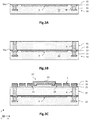
- the figure 1A is a schematic sectional view of a thermal detector 1 similar to that described in the article by Li et al. titled Recent Development of Ultra Small Pixel Uncooled Focal Plane Arrays at DRS, Infrared Technology and Applications XXXIII, Proc. of SPIE, Vol. 6542, 65421Y, 2007 .
- the thermal detector 1 comprises a three-dimensional structure 2 suspended above the substrate 10 by anchoring pillars 4 and thermally insulated therefrom by thermal insulation arms 5.
- the three-dimensional structure 2 comprises a lower stage formed by a membrane 9 containing a thermistor material 6, here a vanadium oxide, and comprises an upper stage formed by an absorber 7 of the incident infrared radiation.
- the absorber 7 extends flatly above the membrane 9, while being in thermal connection with the thermistor material 6. More precisely, the absorber 7 seems to be formed of two parts 7.1, 7.2 made of a in one piece and in the same material: an upper peripheral part 7.1 which extends planarly above the membrane 9, and a vertical central hollow part 7.2 which comes to rest on the membrane 9. However, the presence of the 7.2 vertical central part is likely to degrade the properties of the quarter-wave interference cavity and therefore to reduce the absorption of incident infrared radiation by the absorber 7.
- the thermal detector is liable to be subjected to high-power electromagnetic radiation, such as solar radiation or laser radiation.
- the absorbent membrane being thermally insulated from the substrate, it can then undergo a strong heating capable of causing a degradation of the properties of the thermometric transducer.
- the figure 1B is a schematic sectional view of a thermal detector 1 described in the application KR101181248 .
- the absorbent membrane 9 is suspended above the substrate 10 by arms 8 for anchoring and thermal insulation. It is adapted to deform locally under the effect of heating until it comes into contact with the substrate 10. This mechanical and therefore thermal contact causes the cooling of the absorbent membrane 9, thus making it possible to prevent the temperature of that -this does not reach or exceed a threshold temperature T th beyond which a degradation of the properties of the thermistor material can take place.
- the absorbent membrane 9 comprises a fixed detection part 9.1 at the level of which the thermistor material is disposed, and a deformable part 9.2 of the bimetallic strip type suitable for producing a thermal short circuit between the absorbent membrane 9 and the substrate 10.
- the deformable part 9.2 deforms by bimetallic strip effect until it comes into contact with the substrate 10, which causes the cooling of the absorbent membrane 9.
- This cooling in turn causes l spacing of the deformable part 9.2 from the substrate 10.
- a continuous movement of vertical oscillation can take place because of the alternation of the cooling phases in contact with the substrate and reheating after loss of contact, which affects the quality of the thermal contact between the deformable part 9.2 and the substrate 10, and therefore the cooling of the absorbent membrane 9.
- the invention aims to remedy at least in part the drawbacks of the prior art, and more particularly to propose a thermal detector having an absorption of electromagnetic radiation of improved interest, while ensuring good protection against high power electromagnetic radiation.
- thermal detector Some preferred but non-limiting aspects of this thermal detector are as follows.
- the shape memory alloy has a volume fraction ⁇ m of the martensitic phase. It can present the plane configuration of detection when the fraction volume ⁇ m is greater than or equal to 0.95, and may have the cooling curve configuration when the volume fraction ⁇ m is less than 0.95.
- the shape memory alloy may have a volume fraction ⁇ m of less than or equal to 0.05 when its temperature is greater than or equal to a temperature known as final austenitic A f , said final austenitic temperature A f being lower than a predetermined threshold temperature T th of the thermometric transducer.
- the deformable absorber may comprise a fixed part resting in contact with the membrane, and a free part adapted to deform as a function of the temperature of the deformable absorber and extending from the fixed part being spaced from the membrane .
- the shape memory alloy can be a metallic alloy based on NiTi.
- the shape memory alloy can be a metallic alloy chosen from Ti 85.3-x Ni x Hf 14.7 with x> 50% at, Ti 82-x Ni x Zr 18 with x> 49% at, Ti 7 Ni 11 Zr 43 Cu 39-x Co x with x> 10% at, Ti 50 Ni 50-x Pt x with x ⁇ 25% at, Ti 50.5 Ni 24.5 Pd 25 , Ti 51 Ni 38 Cu 11 , Ti 50-x Ni 50 Cu x with x> 7.5% at, or even an alloy based on TiNiCuAlMn.
- the deformable absorber may include an absorbent layer made of the shape memory alloy having protuberances arranged on a face of the absorbent layer opposite the substrate.
- the deformable absorber may include an absorbent layer of the shape memory alloy having at least one notch formed from a face of the absorbent layer opposite the substrate.
- the substrate may have a flat upper face, and in which the three-dimensional structure is held above the upper face of the substrate by thermal insulation arms, and by anchoring pillars which extend substantially orthogonal to the plane of the upper face of the substrate.
- the substrate may include a reading circuit, the three-dimensional structure being electrically connected to the reading circuit by the anchoring pillars and by the thermal insulation arms.
- the invention relates to a device for detecting electromagnetic radiation, for example infrared or terahertz radiation.
- the detection device comprises one or more thermal detectors preferably particularly suitable for detecting infrared radiation from the LWIR ( Long Wavelength Infrared ) range, the wavelength of which is between approximately 8 ⁇ m and 14 ⁇ m.
- LWIR Long Wavelength Infrared
- Each thermal detector has a three-dimensional structure, suspended above the substrate, and thermally isolated from it.
- the three-dimensional structure comprises several distinct functional stages superimposed on each other, that is to say arranged opposite and parallel to each other. It thus comprises a membrane located in a lower stage and containing a thermometric transducer, and an absorber situated in an upper stage.
- the absorber is adapted to absorb the electromagnetic radiation to be detected, and rests on the membrane while being partly spaced therefrom, and is in thermal connection with the thermometric transducer.
- Each thermal detector also includes a reflector of the electromagnetic radiation to be detected, preferably located on the substrate.
- the absorber is spaced with respect to the reflector so as to form a quarter-wave interference cavity, thus making it possible to optimize the absorption of the infrared radiation to be detected by the absorber.
- the absorber is said to be deformable and is adapted to deform as a function of its temperature, thereby passing from a first configuration known as detection when its temperature is less than or equal to a first predetermined threshold temperature T 1 , to a second so-called cooling configuration when its temperature is greater than a second predetermined threshold temperature T 2 , and vice versa.
- the absorber In the detection configuration, the absorber extends planarly in a plane parallel to the plane of the reflector, thereby making it possible to maximize the absorption of the electromagnetic radiation to be detected.
- the absorber In the cooling configuration, the absorber extends in a curved manner with respect to a plane parallel to the plane of the reflector, thus minimizing the absorption of the electromagnetic radiation to be detected.
- the temperature T of the deformable absorber is substantially equal to the temperature of the membrane, due to the thermal bond between these two elements. Also, the temperature is assumed to be homogeneous, at first order, within the three-dimensional structure, that is to say both in the deformable absorber and in the membrane with thermometric transducer.
- the deformable absorber is made based on at least one shape memory alloy (SMA, for Shape Memory Alloy, in English), that is to say an alloy having a martensitic transformation.
- shape memory alloy SMA, for Shape Memory Alloy, in English
- the deformable absorber mainly comprises said shape memory alloy.
- a martensitic transformation is a structural transition of the alloy, reversible and displacive type, depending on the temperature, between a martensitic phase (crystallographic phase at low temperature) and an austenitic phase (crystallographic phase at high temperature).
- the martensitic transformation has characteristic temperatures (at zero stress) which depend on the direction of the transformation.
- the temperatures of beginning and end of transformation are conventionally noted M s (for Martensite start temperature, in English) and M f (for Martensite finish temperature ).
- M s for Martensite start temperature
- M f for Martensite finish temperature
- a s for Austenite start temperature
- a f for Austenite finish temperature
- the martensitic transformation exhibits a temperature hysteresis between the cooling and the heating of the alloy, insofar as the temperatures M s and A f are different from each other, just as are temperatures M f and A s .
- the volume fraction ⁇ m of the martensitic phase is greater than or equal to 0.95, or even equal to 1.0, when the temperature T of the shape memory alloy is lower or equal to the temperature A s . It then decreases as the temperature T increases and is less than or equal to 0.05, or even equal to 0, when the temperature T is greater than or equal to the temperature A f .
- the volume fraction ⁇ m of the martensitic phase is less than or equal to 0.05, or even equal to 0, when the temperature T of the shape memory alloy is greater than or equal to the temperature M s . It then increases as the temperature T decreases and is greater than or equal to 0.95, or even equal to 1.0, when the temperature T is less than or equal to the temperature M f .
- the threshold effect associated with the deformation of the shape memory alloy is used to minimize the risks of degradation of the thermometric transducer linked to excessive heating, while optimizing the absorption of the electromagnetic radiation of interest in the absence of such excessive heating.
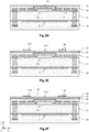
- FIGS. 2A and 2B are schematic sectional views of a thermal detector 1 according to one embodiment, comprising a deformable absorber 30 in planar detection configuration ( fig.2A ) and in cooling curve configuration ( fig. 2B ).
- a single thermal detector 1 is shown here, but the detection device advantageously comprises a matrix of identical thermal detectors (sensitive pixels).
- the thermal detector 1 can have lateral dimensions in the XY plane (say not pixel), of the order of one to a few tens of microns, for example equal to about 10 ⁇ m or even less.
- a direct three-dimensional orthogonal coordinate system (X, Y, Z), where the plane (X, Y) is substantially parallel to the main plane of the reading substrate 10 of the thermal detector 1, and where l Z axis is oriented in a direction substantially orthogonal to the main plane of the reading substrate 10 and oriented towards the three-dimensional structure 2.
- the terms “lower” and “upper” are understood to relate to a increasing positioning when moving away from the reading substrate 10 in the + Z direction.
- the thermal detector 1 comprises an advantageously functionalized substrate, called the reading substrate 10, produced in this example based on silicon, comprising a reading circuit allowing the control and the reading of the thermal detectors.
- the read circuit is here in the form of a CMOS integrated circuit located in a support substrate 11. It includes portions 13 of conductive lines, for example metallic, separated from each other by a dielectric material 12, for example a mineral material based on silicon such as a silicon oxide SiO x , a silicon nitride SiN x , or their alloys.
- the thermal detector 1 may also include active electronic elements (not shown), for example diodes, transistors, or passive electronic elements, for example capacitors, resistors, etc., connected by electrical interconnections to the thermal detector 1 on the one hand, and on the other hand to a connection pad (not shown), the latter being intended to connect the detection device to an external electronic device.
- the conductive portions 13 and the conductive vias 14 can be made, for example, of copper, aluminum or tungsten.
- the copper or tungsten may optionally be located between sublayers made of titanium nitride, tantalum or the like.
- the reading substrate 10 here has an upper face 10a formed in particular by a surface of an inter-metal insulating layer 12 and a surface of conductive portions 13 of the last level of electrical interconnection.
- the thermal detector 1 comprises a reflector 3, made of at least one material reflecting with respect to the electromagnetic radiation to be detected. It is advantageously formed here of a portion of the conductive line of the last level of electrical interconnection of the CMOS integrated circuit. It is located here in the substrate 10 and participates in defining the upper face 10a of the substrate. Alternatively, it can rest on the upper face 10a of the substrate, or even be spaced from the latter by a non-zero distance.
- the upper face 10a is advantageously coated with a protective layer 15, in particular when the thermal detector 1 is produced by using mineral sacrificial layers then eliminated by chemical attack in HF acid medium (hydrofluoric acid).
- the protective layer 15 then has an etching stop function, and is therefore suitable for ensuring protection of the support substrate 11 and of the inter-metal dielectric layers 12, when they are made of an inorganic material, with respect to HF chemical attack screw.
- This protective layer 15 thus forms a hermetic and chemically inert layer. It is electrically insulating to avoid any short circuit between the portions 13 of metal line. It can thus be produced in alumina Al 2 O 3 , or even in aluminum nitride or fluoride, or even in intrinsic amorphous silicon. It may have a thickness between a few tens and a few hundred nanometers, for example between 10nm and 500nm, preferably between 20nm and 100nm.
- the thermal detector 1 comprises a three-dimensional structure 2 adapted to detect the electromagnetic radiation of interest, suspended above the substrate 10 by the anchoring pillars 4 and thermally insulated therefrom by thermal insulation arms 5.
- the three-dimensional structure 2 is moreover electrically connected to the reading circuit by the anchoring pillars 4 and the thermal insulation arms 5.
- the anchoring pillars 4 are conductive pads made of at least one electrically conductive material, which extend along the axis Z from the reading substrate 10 to the three-dimensional structure 2. They are in contact with the portions 13 conductive lines, and thus ensure the electrical connection of the three-dimensional structure 2 to the reading circuit.
- the anchoring pillars 4 can be made, for example, of copper, aluminum or tungsten, optionally encapsulated in at least one protective sublayer of titanium nitride, or the like.
- the thermal insulation arms 5 here extend substantially coplanar with the membrane 20, and are here formed of a layer electrically conductive allowing the electrical connection of the membrane 20 to the reading circuit, advantageously encapsulated in two lower and upper dielectric layers which help to stiffen the thermal insulation arms 5.
- the three-dimensional structure 2 has two separate functional stages superimposed on each other.
- the functional stages are thus arranged in separate planes which are parallel to each other, and are opposite one another.
- the first functional stage is a lower stage having a function for detecting electromagnetic radiation.
- it comprises the membrane 20 containing a thermometric transducer 23, that is to say an element having an electrical property varying with its heating.
- the membrane 20 extends planarly parallel to the plane XY of the substrate 10. It is said to be fixed in so far as it is located at a substantially constant distance from the substrate 10.
- the thermometric transducer 23 is here a material thermistor such as for example a vanadium or titanium oxide, or amorphous silicon, but may alternatively be a capacitor formed by a pyroelectric or ferroelectric material, a diode (pn or pin junction), or even a field effect transistor and at metal / oxide / semiconductor structure (MOSFET).
- the membrane 20 is here conventionally formed of a stack of a lower dielectric layer 21 made of a dielectric material, of two electrodes 22 electrically isolated from one another by lateral spacing, of a thermistor material 23 s' extending in contact with the polarization electrodes 22 and the lower dielectric layer 21, and with an upper dielectric layer 24 covering the polarization electrodes 22 and the thermistor material 23, making it possible in particular to protect the thermistor material 23 during chemical attack hydrofluoric acid implemented later.
- the second functional stage is an upper stage having a function of absorbing the electromagnetic radiation to be detected. It thus comprises the deformable absorber 30, produced on the basis of a shape memory alloy advantageously adapted to absorb electromagnetic radiation. It rests on the membrane 20 and is in thermal connection with the thermistor material 23, while being partly spaced from the latter.
- the deformable absorber 30 is thus adapted to deform as a function of its temperature and thus to pass from a planar detection configuration to a cooling curve configuration, and vice versa.
- the deformable absorber 30 is formed of a fixed part 30.1, resting in contact with the membrane 20, here of the upper protective layer, and of a so-called free part 30.2, that is to say able to deform and spaced from the membrane 20 by a non-zero distance.
- the fixed part 30.1 is located in the center of the deformable absorber 30, and the part free 30.2 extends peripherally around the fixed part 30.1.
- the fixed part 30.1 can be located on the edge of the deformable absorber 30, and the free part 30.2 can then extend from the fixed part 30.1 in one or two preferred directions.
- the deformable absorber 30 is adapted to occupy a detection configuration in which it extends planarly parallel to the XY plane of the substrate.
- the deformable absorber 30 can occupy the plane configuration of detection when the shape memory alloy has a volume fraction ⁇ m of the martensitic phase greater than or equal to 0.95, for example equal to 1.0, that is to say when its temperature is less than or equal to a first threshold temperature T 1 , namely the final martensitic temperature M f or the initial austenitic temperature A s according to the direct or opposite direction of the martensitic transformation.
- the deformable absorber 30 is planar, so that its fixed part 30.1 and its free part 30.2 are spaced from the reflector 3 by a non-zero distance d d substantially constant and homogeneous in the XY plane.
- the distance d d is therefore constant in temperature as long as T is less than or equal to T 1 .
- This distance is adjusted so as to form an undisturbed quarter-wave interference cavity maximizing the absorption of the electromagnetic radiation to be detected by the deformable absorber 30.
- the deformable absorber 30 is spaced from the reflector 3 by a distance typically between 1 ⁇ m and 5 ⁇ m, preferably 2 ⁇ m, when the thermal detector 1 is designed for the detection of infrared radiation included in the LWIR.
- the deformable absorber 30, in the planar detection configuration makes it possible to maximize the absorption of the electromagnetic radiation of interest.
- the deformable absorber 30 is adapted to occupy a cooling configuration for which the absorber extends in a curved manner with respect to a plane parallel to the plane XY of the substrate. It can occupy the cooling curve configuration when the shape memory alloy has a volume fraction ⁇ m of the martensitic phase less than 0.95, for example equal to 0.5 or less, that is to say when its temperature is higher at a second predetermined threshold temperature T 2 , namely here the initial austenitic temperature A s .
- the deformable absorber 30 is curved, so that its fixed part 30.1 is spaced from the reflector 3 by the distance d d but that the deformed free part 30.2 is spaced from the reflector 3 by a non-zero distance variable d r in the XY plane, whose value depends on the temperature T.
- This distance d r no longer corresponds to the distance d d so that the quarter-wave interference cavity is degraded.
- the absorption of electromagnetic radiation by the deformable absorber 30, in the the cooling curve configuration is then reduced, which makes it possible to reduce the heating of the deformable absorber 30 and therefore to reduce its temperature as well as that of the thermistor material 23.
- the deformable absorber 30 is made from a shape memory alloy. It is formed by an absorbent layer 32 of the shape memory alloy, here advantageously encapsulated between two lower and upper protective layers (cf. fig.3A-3H ).
- the protective layers are intended to protect in particular the shape memory alloy during a phase of removal of the sacrificial layers used during the manufacture of the thermal detector 1. They can be produced for example from a silicon nitride SiN or a silicon oxide SiO, for example with a thickness of 10 nm.
- the shape memory alloy is a metal alloy chosen from alloys based on NiTi, based on copper Cu, or based on iron Fe.
- the metal alloy is chosen so that the temperature initial austenitic A s is equal to the temperature T 2 , which is less than or equal to a predetermined temperature T th for protecting the thermometric transducer.
- This protection temperature depends on the type of thermometric transducer, and can be of the order of 100 ° C to 350 ° C, for example at 200 ° C.
- the metal alloy can be produced in a binary compound NiTi with an atomic proportion of nickel and titanium equal or not, or in a ternary compound NiTiA where the additional chemical element A can be iron Fe, copper Cu, zirconium Zr, hafnium Hf, platinum Pt, palladium Pd, tungsten W, gold Au, or the like. It can thus be Ti 51 Ni 38 Cu 11 where the indices represent the atomic proportion of each chemical element within the alloy.
- the thickness of the absorbent layer 32 in the shape memory alloy is such that its impedance is substantially equal to that of the vacuum (resistance of the absorbent layer close to 377 ⁇ / sq) and can be between a few nanometers to a few tens of nanometers, for example between 5nm and 25nm.
- the metal alloy is Ti 50-x Ni 50 Cu x (resistivity 1.5x10 -6 ⁇ .m) of thickness between 4nm and 6nm, and Ti 85.3-x Ni x Hf 14.7 (resistivity 2x10 -6 ⁇ .m) of thickness between 5nm and 10nm.
- the absorbent layer 32 made of the shape memory alloy advantageously has a constant thickness in the fixed part 30.1 and the free part 30.2.
- it may include protuberances 34 (cf. fig.3H ) located at the level of the free part 30.2, and / or at least one notch 35 (cf. fig.3H ) located at the joint between the fixed part 30.1 and the free part 30.2.
- the absorbent layer 32 made of the shape memory alloy of the deformable absorber 30 advantageously comprises a local thickness variation, so as to more effectively control the direction of the deformation between the planar and curved configurations.
- the absorbent layer 32 in the shape memory alloy comprises at least one protruding pattern 34 (cf. fig.3H ), that is to say at least one protuberance, situated on a face of the deformable absorber 30 opposite the substrate 10.
- these protuberances 34 may extend orthogonally to the local surface of the deformable absorber 30, and can have a height for example of the order of a few tens of nanometers.
- the deformable absorber 30 may also include at least one notch 35 (cf. fig.3H ) located at the joint between the fixed part 30.1 and the movable part, at the face of the deformable absorber 30 opposite the substrate 10.
- a notch 35 is a local decrease in the thickness of the absorbent layer 32 in l shape memory alloy, which remains non-zero.
- the deformable absorber 30 is made of a shape memory alloy having a dynamic time constant ⁇ t dyn of deformation, in response to the absorption of high power electromagnetic radiation, which is less than a thermal time constant ⁇ t th associated with the excessive heating caused by this radiation.
- the thermal detector 1 receives high power electromagnetic radiation
- the deformable absorber 30 deforms and changes from the planar detection configuration to the cooling curve configuration, which causes a disturbance of the quarter interference cavity. wave and therefore a degradation of the absorption of electromagnetic radiation, and therefore a decrease in the temperature T of the deformable absorber 30, before the temperature T reaches the threshold temperature T th of protection of the thermistor material 23.
- the shape memory alloy is advantageously chosen from, for example, Ti 85.3-x Ni x Hf 14.7 with x> 50% in at.%, Ti 50-x Ni 50 Cu x with x> 7.5% in at.%, Ti 82-x Ni x Zr 18 with x> 49% in at.%, Ti 50.5 Ni 24.5 Pd 25 , among others.
- the deformable absorber 30 based on a shape memory alloy makes it possible to improve the protection of the thermal detector 1, and more precisely of the thermometric transducer 23, when the latter is subjected to high power electromagnetic radiation.
- the temperature T of the deformable absorber 30 is equal to a nominal temperature, which is less than or equal to the initial austenitic temperature A s .
- the deformable absorber 30 thus has a planar detection configuration, in which it extends in a substantially planar manner opposite the reflector 3. The quarter-wave interference cavity is thus not degraded, which makes it possible to maximize the absorption of the electromagnetic radiation of interest by the deformable absorber 30.
- the temperature T of the deformable absorber 30 increases and becomes higher than the initial austenitic temperature A s .
- the deformable absorber 30 thus passes from the planar detection configuration to the cooling curve configuration, in which it extends in a substantially curved manner with respect to the XY plane parallel to the reflector 3.
- the properties of the quarter interference cavity wave are then degraded, which causes a decrease in the absorption of high power electromagnetic radiation by the deformable absorber 30, and leads to a decrease in temperature T.
- the threshold effect linked to the reverse martensitic transformation of a shape memory alloy is thus used to protect the thermal detector 1 from excessive heating, while keeping a quarter interference cavity wave not degraded in the absence of such high power electromagnetic radiation.
- the thermal detector 1 is produced using mineral sacrificial layers intended to be subsequently removed by wet etching in an acid medium (HF vapor).
- the sacrificial layers may be made on the basis of polyimide or equivalent and be subsequently removed by dry etching, for example under plasma 02.
- the materials of the protective layers 31, 33 are adapted to be inert to this type of dry etching, and can be chosen from AlN, Al 2 O 3 , amorphous carbon, amorphous silicon, among others.
- the reading substrate 10 is produced, formed of a support substrate 11 containing the reading circuit suitable for controlling and reading the thermal detector 1.
- the reading circuit thus comprises conductive portions 13 which are flush with the upper face 10a of the substrate reading 10, which is substantially planar.
- the conductive portions 13 and the conductive vias 14 can be made of copper, aluminum and / or tungsten, among others, for example by means of a damascene process in which are filled with trenches made in the inter-metal insulating layer.
- the outcrop of the conductive portions 13 at the level of the upper face 10a can be obtained by a chemical mechanical planarization technique (CMP).
- CMP chemical mechanical planarization technique
- the reflector 3 of the thermal detector 1 is also produced.
- the reflector 3 is here formed by a portion of a conductive line of the last interconnection level, this being made of a metallic material suitable for reflecting the electromagnetic radiation to be detected. It is intended to extend opposite the membrane 20, and is intended to form with the deformable absorber 30 a quarter-wave interference cavity with respect to the electromagnetic radiation to be detected.
- a protective layer 15 can then be deposited so as to cover the inter-metal insulating layer 12.
- This etching stop layer 15 is made of a material substantially inert to the etching agent used subsequently to remove the mineral sacrificial layers , for example in the HF vapor phase medium. It thus prevents the underlying mineral insulating layers 12 from being etched during this step of removing the sacrificial layers. It can be formed from an aluminum oxide or nitride, from aluminum trifluoride, or from intrinsic amorphous silicon (not intentionally doped). It can be deposited for example by PVD (for Physical Vapor Deposition, in English) and can have a thickness of the order of ten nanometers to a few hundred nanometers.
- a first sacrificial layer 41 is deposited on the reading substrate 10, for example made of an inorganic material such as a silicon oxide SiO x deposited by chemical vapor deposition plasma assisted (PECVD).
- This mineral material is capable of being removed by wet chemical etching, in particular by chemical attack in an acid medium, the etchant preferably being hydrofluoric acid (HF) in the vapor phase.
- This mineral sacrificial layer 41 is deposited so as to extend continuously over substantially the entire surface of the reading substrate 10 and thus cover the etching stop layer 15.
- the thickness of the sacrificial layer 41 along the axis Z allows to define the height of the membrane 20. It can be of the order of a few hundred nanometers to a few microns.
- Vertical holes are then made for forming the anchoring pillars 4. They are made by photolithography and etching, and pass through the mineral sacrificial layer 41 and the protective layer 15, to lead to the conductive portions 13 of the reading circuit. .
- the vertical orifices may have a cross section in the plane (X, Y) of square, rectangular or circular shape, with a surface substantially equal, for example, to 0.25 ⁇ m 2 .
- the anchoring pillars 4 are then produced in the vertical holes. They can be made by filling the orifices with one or more electrically conductive materials.
- they can each comprise a layer of TiN deposited by PVD or MOCVD (for Metal Organic Chemical Vapor Deposition, in English) on the vertical sides of the orifices, and a core of copper or tungsten filling the defined space. transversely through the TiN layer.
- a CMP step then makes it possible to remove the excess filling materials and to planarize the upper face formed by the sacrificial layer 41 and the anchoring pillars 4.
- the thermal insulation arms 5 and the membrane 20 with thermometric transducer are produced, here a membrane 20 with thermistor.
- the thermal insulation arms 5 provide thermal insulation of the membrane 20 from the reading substrate 10, the electrical connection of the thermistor material 23, and participate in keeping the membrane 20 suspended above the reading substrate. 10.
- a lower dielectric layer 21 is deposited here on the sacrificial layer 41, then a conductive layer 22 and an intermediate dielectric layer 25.
- the electrical contact between the anchoring pillars 4 and the conductive layer 22 is obtained by openings previously made through the lower dielectric layer 21 and filled with the material of the conductive layer 22.
- the conductive layer 22 is thus in contact with the upper end of the anchoring pillars 4.
- the lower dielectric layers 21 and intermediate 25 can be made of amorphous silicon, silicon carbide, alumina Al 2 O 3 or aluminum nitride, among others. They may have a thickness of a few tens of nanometers, for example 20 nm, and participate in ensuring the stiffening of the thermal insulation arms 5.
- the thermistor membrane 20 is formed by a stack here of the lower insulating layer 21, of two electrodes 22 coming from the conductive layer and insulated from one another by lateral spacing, from the intermediate insulating layer 25 covering the polarization electrodes 22 and the lateral spacing, except in two openings leading to the electrodes 22, of a thermistor material 23, for example amorphous silicon or a vanadium or titanium oxide.
- the thermistor material 23 is in contact with the two electrodes 22 via the openings.
- An upper protective layer 26 is then deposited so as to cover the thermistor material 23 and possibly the intermediate dielectric layer 25 at the level of the thermal insulation arms 5.
- a second sacrificial layer 42 is then deposited, then a second lower protective layer 31.
- the second sacrificial layer 42 thus covers the thermistor membrane 20 as well as the thermal insulation arms 5.
- a CMP step can be performed so that the upper face of the sacrificial layer 42 is flush with that of the upper protective layer 26.
- the sacrificial layer 42 is preferably made of a material identical to that of the first sacrificial layer 41.
- the lower protective layer is then deposited 31 so as to cover the second sacrificial layer 42. It is preferably made of a material making it possible to protect the shape memory alloy during a subsequent step of removing the sacrificial layers. It can be made of a nitride or a silicon oxide, with a thickness for example of 10 nm.
- an absorbent layer 32 made of a shape memory alloy is then deposited.
- the absorbent layer 32 is deposited so as to cover the lower protective layer 31. It has a constant thickness at the level of the fixed and free parts, chosen so as to adapt its impedance to that of the vacuum. The thickness can thus be between 5 nm and 25 nm, for example.
- the shape memory alloy can be a metallic alloy of NiTi whose atomic proportion of nickel and titanium, as well as any additional chemical elements, makes it possible to obtain an initial austenitic temperature A s equal to the temperature T 2 and below a protection threshold temperature T th .
- the shape memory alloy can thus be chosen from Ti 85.3-x Ni x Hf 14.7 with x> 50% in at.%, Ti 82-x Ni x Zr 18 with x> 49% in at.%, Ti 7 Ni 11 Zr 43 Cu 39-x Co x with x> 10% in at.%, Ti 50 Ni 50-x Pt x with x ⁇ 25% in at.%, Ti 50,5 Ni 24.5 Pd 25 , Ti 51 Ni 38 Cu 11 , Ti 50-x Ni 50 Cu x with x> 7.5% at at%, or even an alloy of the TiNiCuAlMn family.
- protruding patterns 34 that is to say protuberances, are advantageously produced from the shape memory alloy.
- protrusions 34 are arranged at a face of the absorbent layer 32 opposite the substrate 10 and are located in an area intended to form the free part 30.2. They can extend, continuously or not, around the fixed part 30.1. Also, the zones intended to form the fixed 30.1 and free 30.2 parts have a substantially constant thickness, except at the level of the protrusions 34.
- the thickness of the protrusions 34 may be of the order of 5 nm to 100 nm, and preferably be between 10nm and 50nm.
- a second upper protective layer 33 is then deposited, so as to continuously cover the absorbent layer 32 in the alloy with shape memory.
- the upper protective layer 33 therefore extends over the zones intended to form the fixed 30.1 and free 30.2 parts, and covers the protrusions 34. It is preferably made of a material and a thickness identical to those of the lower protective layer 31.
- the stack of lower 31 and upper 33 protective layers is then structured, as well as the absorbent layer 32, by photolithography and etching, so as to form the deformable absorber 30 disposed opposite the reflector 3.
- the deformable absorber 30 thus comprises a fixed part 30.1 resting in contact with the membrane 20, and a part 30.2 here peripheral intended to be free, that is to say capable of deforming as a function of its temperature.
- a notch 35 is advantageously produced, by partial etching of the absorbent layer 32 and the upper protective layer 33, located at the joint between the fixed part 30.1 and the free part 30.2.
- the notch 35 can be produced before the deposition of the upper protective layer 33.
- the various sacrificial layers 41, 42 are removed so as to suspend the three-dimensional structure 2, and therefore the membrane 20 above the reading substrate 10, and the free part 30.2 of the deformable absorber 30 above the membrane 20.
- the suspension can be carried out after having encapsulated the thermal detector 1 in a box (not shown) defining a vacuum cavity intended to be hermetic.
- the suspension can be obtained by chemical etching of the various mineral sacrificial layers 41, 42, here by wet chemical etching by attack with hydrofluoric acid in the vapor phase.
- a thermal detector 1 comprising a three-dimensional structure 2 formed by a lower stage containing the membrane 20 with thermistor, and an upper stage containing the deformable absorber 30.
- This is formed on the basis of a memory alloy of shape which makes it possible to ensure the deformation of the deformable absorber 30 and to absorb the electromagnetic radiation of interest. It comprises a fixed part 30.1 which rests in contact with the membrane 20 with thermistor, and a free part 30.2 which is spaced from the latter.
- the deformable absorber 30 has a plane detection configuration, in which it is spaced from the reflector 3 by the constant distance d d in the plane XY.
- the quarter-wave interference cavity is then undisturbed, which maximizes the absorption of the electromagnetic radiation of interest by the deformable absorber 30.
- the deformable absorber 30 Above this temperature A s , the deformable absorber 30 has a curved configuration of cooling in which the free part 30.2 is spaced from the reflector 3 by a distance d r different from the value d d .
- the quarter-wave interference cavity is then disturbed, which reduces the absorption of high power electromagnetic radiation by the deformable absorber 30 and causes its cooling and therefore that of the membrane 20 with thermistor.
- the thermal detector 1 thus has improved protection against high power electromagnetic radiation, while optimizing the absorption of the electromagnetic radiation of interest in the absence of excessive heating.
- the shape memory alloy has a dynamic time constant ⁇ t day advantageously less than the thermal time constant ⁇ t th associated with the heating of the deformable absorber 30 when it is subjected to radiation electromagnetic of high power
- the shape memory alloy deforms and quickly passes from the plane detection configuration to the cooling curve configuration, thus limiting any excessive heating of the deformable absorber 30 and therefore of the membrane 20 with thermistor, and therefore any risk of degradation of the thermistor material 23.
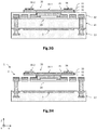
- the figure 4A illustrates an alternative embodiment which differs from the embodiment illustrated on the fig.3H essentially in that the membrane 20 comprises an intermediate portion 27 which rests on the thermistor material 23, here on the upper protective layer 26.
- the intermediate portion 27 is made of a thermally conductive material. Here it is located in the center of the membrane 20 and here in the center of the thermistor material 23. It has an upper face forming the support surface for the deformable absorber 30.
- the support surface has an extent less than that of the upper protective layer 26 at the thermistor material 23.
- the deformable absorber 30 then has a deformation length, in the XY plane, greater than if it rested in contact with the upper protective layer 26.
- the deformable absorber 30, in the cooling curve configuration has a free part 30.2, adapted to deform, which extends peripherally around a fixed part 30.1 which rests on the intermediate portion 27.
- the free part 30.2 has a surface in the plane Larger XY, which leads to disturb the quarter-wave interference cavity over a larger area in the XY plane, and therefore leads to a decrease greater the absorption of the electromagnetic radiation of interest, and therefore the temperature of the deformable absorber 30.
- the figure 4B schematically illustrates another variant, which differs from that illustrated on the fig. 4A essentially in that the intermediate portion 27 is located at the edge of the thermistor material 23. Also, the deformable absorber 30 has a free part 30.2, adapted to deform, located opposite the thermistor material 23, which extends in the plane XY from the fixed part 30.1.
- the fig.4B illustrates another example of the structure of the membrane 20.
- the membrane 20 does not comprise an intermediate dielectric layer situated between the thermistor material 23 and the polarization electrodes 22. It thus comprises a lower dielectric layer 21, produced in a dielectric material, for example made of a silicon oxide, a silicon nitride or a silicon oxynitride. It can also be made of a semiconductor material having an electrical resistivity lower than dielectric materials, but having a lower thermal conductivity, such as amorphous silicon of high electrical resistivity.
- the lower dielectric layer 21 can be made of amorphous silicon with a thickness of 40 nm and a higher electrical resistivity or equal to 1000 ⁇ .cm.
- the lower dielectric layer 21 has a thickness, for example between 10 nm and 100 nm, preferably between 30 nm and 50 nm. It helps to stiffen the thermal insulation arms 5.
- Two polarization electrodes 22 extend planarly over and in contact with the lower dielectric layer 21. They are spaced from one another by a lateral spacing for example of the order of 5 ⁇ m to 10 ⁇ m for a pixel pitch of the order of 12 ⁇ m, so as to avoid electrically shunting the thermistor material 23.
- the material thermistor 23 rests in contact with the polarization electrodes 22, and rests in contact with the lower dielectric layer 21.
- An upper dielectric layer 24 covers the thermistor material 23 and the polarization electrodes 22. It preferably has a material identical or similar to that of the lower dielectric layer 21, and preferably has an identical thickness. It advantageously participates in the stiffening of the thermal insulation arms 5.
- This example of membrane 20 is given by way of illustration, and other structures can be used.
Landscapes
- Physics & Mathematics (AREA)
- General Physics & Mathematics (AREA)
- Spectroscopy & Molecular Physics (AREA)
- Condensed Matter Physics & Semiconductors (AREA)
- Electromagnetism (AREA)
- Engineering & Computer Science (AREA)
- Computer Hardware Design (AREA)
- Microelectronics & Electronic Packaging (AREA)
- Power Engineering (AREA)
- Chemical & Material Sciences (AREA)
- Inorganic Chemistry (AREA)
- Photometry And Measurement Of Optical Pulse Characteristics (AREA)
- Micromachines (AREA)
Abstract
L'invention porte sur un détecteur thermique comportant une structure tridimensionnelle (2) adaptée à détecter un rayonnement électromagnétique, suspendue au-dessus et thermiquement isolée d'un substrat (10), comportant une membrane (20) et un absorbeur (30), celui-ci étant formé à base d'un alliage à mémoire de forme et étant adapté à présenter une configuration plane de détection lorsque sa température est inférieure ou égale à T<sub>1</sub>et une configuration courbe de refroidissement lorsque sa température est supérieure à une température austénitique initiale A<sub>s</sub>.
Description
- Le domaine de l'invention est celui de détecteurs thermiques d'un rayonnement électromagnétique, par exemple infrarouge ou térahertz, comportant une membrane suspendue et thermiquement isolée vis-à-vis d'un substrat. L'invention s'applique notamment au domaine de l'imagerie infrarouge ou térahertz, de la thermographie, voire de la détection de personne ou de mouvement.
- Les dispositifs de détection de rayonnement électromagnétique peuvent comporter une matrice de pixels sensibles contenant chacun un détecteur thermique comportant une membrane absorbante suspendue au-dessus d'un substrat pouvant contenir un circuit de lecture. La membrane absorbante comporte un absorbeur du rayonnement électromagnétique à détecter associé à un transducteur thermométrique dont une propriété électrique varie en intensité en fonction de l'échauffement du transducteur. Le transducteur thermométrique peut être un matériau thermistance tel qu'un oxyde de vanadium ou du silicium amorphe, entre autres. L'absorbeur est espacé d'un réflecteur disposé au niveau du substrat de manière à former ensemble une cavité interférentielle quart d'onde améliorant l'absorption du rayonnement électromagnétique d'intérêt.
- La température du transducteur thermométrique étant cependant grandement dépendante de son environnement, la membrane absorbante est isolée thermiquement du substrat et du circuit de lecture. Ainsi, la membrane absorbante peut être suspendue au-dessus du substrat par des piliers d'ancrage, et est isolée thermiquement du substrat par des bras d'isolation thermique. Ces piliers d'ancrage et bras d'isolation thermique présentent également une fonction électrique en assurant la connexion électrique de la membrane absorbante au circuit de lecture.
- La
figure 1A est une vue schématique en coupe d'un détecteur thermique 1 similaire à celui décrit dans l'article de Li et al. intitulé Recent Development of Ultra Small Pixel Uncooled Focal Plane Arrays at DRS, Infrared Technology and Applications XXXIII, Proc. of SPIE, Vol. 6542, 65421Y, 2007. Le détecteur thermique 1 comporte une structure tridimensionnelle 2 suspendue au-dessus du substrat 10 par des piliers d'ancrage 4 et thermiquement isolée de celui-ci par des bras d'isolation thermique 5. La structure tridimensionnelle 2 comporte un étage inférieur formé par une membrane 9 contenant un matériau thermistance 6, ici un oxyde de vanadium, et comporte un étage supérieur formé par un absorbeur 7 du rayonnement infrarouge incident. L'absorbeur 7 s'étend de manière plane au-dessus de la membrane 9, tout en étant en liaison thermique avec le matériau thermistance 6. Plus précisément, l'absorbeur 7 semble être formé de deux parties 7.1, 7.2 réalisées d'un seul tenant et en un même matériau : une partie périphérique supérieure 7.1 qui s'étend de manière planaire au-dessus de la membrane 9, et une partie centrale verticale 7.2 creuse, qui vient reposer sur la membrane 9. Cependant, la présence de la partie centrale verticale 7.2 est susceptible de dégrader les propriétés de la cavité interférentielle quart d'onde et donc de diminuer l'absorption du rayonnement infrarouge incident par l'absorbeur 7. - Par ailleurs, le détecteur thermique est susceptible d'être soumis à un rayonnement électromagnétique de forte puissance, tel qu'un rayonnement solaire ou un rayonnement laser. La membrane absorbante étant isolée thermiquement du substrat, elle peut alors subir un fort échauffement susceptible de provoquer une dégradation des propriétés du transducteur thermométrique.
- A ce titre, la
figure 1B est une vue schématique en coupe d'un détecteur thermique 1 décrit dans la demandeKR101181248 - Aussi, lors d'un échauffement excessif de la membrane absorbante 9, la partie déformable 9.2 se déforme par effet bilame jusqu'à venir au contact du substrat 10, ce qui provoque le refroidissement de la membrane absorbante 9. Ce refroidissement provoque en retour l'écartement de la partie déformable 9.2 vis-à-vis du substrat 10. Cependant, il apparaît qu'un mouvement continu d'oscillation verticale peut se mettre en place à cause de l'alternance des phases de refroidissement au contact du substrat et de réchauffement après perte du contact, ce qui nuit à la qualité du contact thermique entre la partie déformable 9.2 et le substrat 10, et donc au refroidissement de la membrane absorbante 9.
- L'invention a pour objectif de remédier au moins en partie aux inconvénients de l'art antérieur, et plus particulièrement de proposer un détecteur thermique présentant une absorption du rayonnement électromagnétique d'intérêt améliorée, tout en assurant une bonne protection vis-à-vis des rayonnements électromagnétiques de forte puissance.
- Pour cela, l'objet de l'invention est un détecteur thermique adapté à détecter un rayonnement électromagnétique, comportant :
- ∘ un substrat ;
- ∘ un réflecteur dudit rayonnement électromagnétique ;
- ∘ une structure tridimensionnelle adaptée à détecter ledit rayonnement électromagnétique, suspendue au-dessus du substrat et thermiquement isolée du substrat, comportant :
- une membrane comportant un transducteur thermométrique,
- un absorbeur dudit rayonnement électromagnétique,
- ▪ reposant sur la membrane et en partie espacé de celle-ci, et en liaison thermique avec le transducteur thermométrique,
- ▪ espacé vis-à-vis du réflecteur de manière à former une cavité interférentielle quart d'onde pour le rayonnement électromagnétique.
- Selon l'invention, l'absorbeur est :
- formé à base d'un alliage à mémoire de forme présentant une transformation martensitique dite inverse d'une phase martensitique en une phase austénitique dudit alliage à partir d'une température dite austénitique initiale As, et
- adapté à présenter :
- ▪ une configuration dite de détection lorsque sa température est inférieure ou égale à une première température seuil T1, dans laquelle il s'étend de manière planaire dans un plan parallèle au réflecteur, et
- ▪ une configuration dite de refroidissement lorsque sa température est supérieure à une deuxième température seuil T2 prédéterminée égale à la température austénitique initiale As, dans laquelle il s'étend au moins en partie de manière courbe vis-à-vis d'un plan parallèle au réflecteur.
- Certains aspects préférés mais non limitatifs de ce détecteur thermique sont les suivants.
- L'alliage à mémoire de forme présente une fraction volumique χm de la phase martensitique. Il peut présenter la configuration plane de détection lorsque la fraction volumique χm est supérieure ou égale à 0.95, et peut présenter la configuration courbe de refroidissement lorsque la fraction volumique χm est inférieure à 0.95.
- L'alliage à mémoire de forme peut présenter une fraction volumique χm inférieure ou égale à 0.05 lorsque sa température est supérieure ou égale à une température dite austénitique finale Af, ladite température austénitique finale Af étant inférieure à une température seuil Tth prédéterminée de protection du transducteur thermométrique.
- L'absorbeur déformable peut comporter une partie fixe reposant au contact de la membrane, et une partie libre adaptée à se déformer en fonction de la température de l'absorbeur déformable et s'étendant à partir de la partie fixe en étant espacée de la membrane.
- L'alliage à mémoire de forme peut être un alliage métallique à base de NiTi. L'alliage à mémoire de forme peut être un alliage métallique choisi parmi le Ti85.3-xNixHf14.7 avec x>50%at, le Ti82-xNixZr18 avec x>49%at, le Ti7Ni11Zr43Cu39-xCox avec x>10%at, le Ti50Ni50-xPtx avec x< 25%at, le Ti50,5Ni24.5Pd25, le Ti51Ni38Cu11, le Ti50-xNi50Cux avec x>7.5 %at, voire un alliage à base de TiNiCuAlMn.
- L'absorbeur déformable peut comporter une couche absorbante en l'alliage à mémoire de forme présentant des protubérances disposées sur une face de la couche absorbante opposée au substrat.
- L'absorbeur déformable peut comporter une couche absorbante en l'alliage à mémoire de forme présentant au moins une échancrure formée à partir d'une face de la couche absorbante opposée au substrat.
- Le substrat peut présenter une face supérieure plane, et dans lequel la structure tridimensionnelle est maintenue au-dessus de la face supérieure du substrat par des bras d'isolation thermique, et par des piliers d'ancrage qui s'étendent de manière sensiblement orthogonale au plan de la face supérieure du substrat.
- Le substrat peut comporter un circuit de lecture, la structure tridimensionnelle étant électriquement connectée au circuit de lecture par les piliers d'ancrage et par les bras d'isolation thermique.
- L'invention porte également sur un procédé de fabrication du détecteur thermique selon l'une quelconque des caractéristiques précédentes, comportant les étapes suivantes :
- fourniture d'un substrat ;
- dépôt sur le substrat d'au moins une première couche sacrificielle ;
- réalisation de piliers d'ancrage au travers de la première couche sacrificielle ;
- réalisation de bras d'isolation thermique et d'une membrane contenant un transducteur thermométrique sur la première couche sacrificielle ;
- dépôt d'au moins une deuxième couche sacrificielle de manière à recouvrir les bras d'isolation thermique et la membrane ;
- réalisation de l'absorbeur sur la deuxième couche sacrificielle, de manière à reposer au moins en partie sur la membrane ;
- suppression des première et deuxième couches sacrificielles.
- D'autres aspects, buts, avantages et caractéristiques de l'invention apparaîtront mieux à la lecture de la description détaillée suivante de formes de réalisation préférées de celle-ci, donnée à titre d'exemple non limitatif, et faite en référence aux dessins annexés sur lesquels :
- les
figures 1A et 1B , déjà décrites, sont des vues schématiques, en coupe (fig.iA) et en perspective (fig.iB), d'un détecteur thermique selon deux exemples de l'art antérieur ; - les
figures 2A et 2B sont des vues schématiques en coupe d'un dispositif de détection selon un mode de réalisation, et lafigure 2C est un graphe qui illustre l'évolution en température de la fraction volumique de la phase martensitique au sein d'un alliage à mémoire de forme ; - les
figures 3A à 3H illustrent différentes étapes d'un procédé de fabrication du dispositif de détection selon une variante du mode de réalisation illustré sur lesfig.2A et 2B ; - les
figures 4A et 4B sont des vues schématiques en coupe de différents détecteurs thermiques selon des variantes de réalisation. - Sur les figures et dans la suite de la description, les mêmes références représentent les éléments identiques ou similaires. De plus, les différents éléments ne sont pas représentés à l'échelle de manière à privilégier la clarté des figures. Par ailleurs, les différents modes de réalisation et variantes ne sont pas exclusifs les uns des autres et peuvent être combinés entre eux. Sauf indication contraire, les termes « sensiblement », « environ », « de l'ordre de » signifient à 10% près, et de préférence à 5% près. Par ailleurs, l'expression « comportant un » doit être comprise, sauf indication contraire, comme « comportant au moins un » et non pas comme « comportant un unique ».
- L'invention porte sur un dispositif de détection d'un rayonnement électromagnétique, par exemple un rayonnement infrarouge ou térahertz. Le dispositif de détection comporte un ou plusieurs détecteurs thermiques de préférence particulièrement adaptés à détecter un rayonnement infrarouge de la gamme LWIR (Long Wavelength Infrared, en anglais) dont la longueur d'onde est comprise entre 8µm et 14µm environ.
- Chaque détecteur thermique comporte une structure tridimensionnelle, suspendue au-dessus du substrat, et thermiquement isolée de celui-ci. La structure tridimensionnelle comporte plusieurs étages fonctionnels distincts et superposés les uns aux autres, c'est-à-dire disposés en regard et parallèlement les uns aux autres. Elle comporte ainsi une membrane située dans un étage inférieur et contenant un transducteur thermométrique, et un absorbeur situé dans un étage supérieur. L'absorbeur est adapté à absorber le rayonnement électromagnétique à détecter, et repose sur la membrane tout en étant en partie espacé de celle-ci, et est en liaison thermique avec le transducteur thermométrique.
- Chaque détecteur thermique comporte également un réflecteur du rayonnement électromagnétique à détecter, situé de préférence sur le substrat. L'absorbeur est espacé vis-à-vis du réflecteur de manière à former une cavité interférentielle quart d'onde, permettant ainsi d'optimiser l'absorption du rayonnement infrarouge à détecter par l'absorbeur.
- Comme détaillé plus loin, l'absorbeur est dit déformable et est adapté à se déformer en fonction de sa température, pour ainsi passer d'une première configuration dite de détection lorsque sa température est inférieure ou égale à une première température seuil T1 prédéterminée, à une deuxième configuration dite de refroidissement lorsque sa température est supérieure à une deuxième température seuil T2 prédéterminée, et inversement. Dans la configuration de détection, l'absorbeur s'étend de manière planaire dans un plan parallèle au plan du réflecteur, permettant ainsi de maximiser l'absorption du rayonnement électromagnétique à détecter. Dans la configuration de refroidissement, l'absorbeur s'étend de manière courbe vis-à-vis d'un plan parallèle au plan du réflecteur, minimisant ainsi l'absorption du rayonnement électromagnétique à détecter. Dans la suite de la description, la température T de l'absorbeur déformable est sensiblement égale à la température de la membrane, du fait de la liaison thermique entre ces deux éléments. Aussi, la température est supposée homogène, au premier ordre, au sein de la structure tridimensionnelle, c'est-à-dire tant dans l'absorbeur déformable que dans la membrane à transducteur thermométrique.
- Pour cela, l'absorbeur déformable est réalisé à base d'au moins un alliage à mémoire de forme (SMA, pour Shape Memory Alloy, en anglais), c'est-à-dire en un alliage présentant une transformation martensitique. Par « à base de », on entend que l'absorbeur déformable comporte majoritairement ledit alliage à mémoire de forme. De manière connue, et comme décrit notamment dans l'article de Choudhary et Kaur intitulé Shape memory alloy thin films and heterostructuresfor MEMS applications: A review, Sensors and Actuators A 242 (2016) 162-181, une transformation martensitique est une transition structurale de l'alliage, réversible et de type displacive, en fonction de la température, entre une phase martensitique (phase cristallographique à basse température) et une phase austénitique (phase cristallographique à haute température). La transformation martensitique présente des températures caractéristiques (à contrainte nulle) qui dépendent du sens de la transformation. Ainsi, pour la transformation directe (austénite en martensite), les températures de début et de fin de transformation sont conventionnellement notées Ms (pour Martensite start temperature, en anglais) et Mf (pour Martensite finish temperature). Pour la transformation inverse (martensite en austénite), les températures de début et de fin de transformation sont conventionnellement notées As (pour Austenite start temperature) et Af (pour Austenite finish temperature). De manière connue également, la transformation martensitique présente une hystérésis en température entre le refroidissement et l'échauffement de l'alliage, dans la mesure où les températures Ms et Af sont différentes l'une de l'autre, tout comme le sont les températures Mf et As.
- En référence à la
figure 2C , lors de la transformation martensitique inverse (de martensite à austénite), la fraction volumique χm de la phase martensitique est supérieure ou égale à 0.95, voire égale à 1.0, lorsque la température T de l'alliage à mémoire de forme est inférieure ou égale à la température As. Elle diminue ensuite à mesure qu'augmente la température T et est inférieure ou égale à 0.05, voire égale à 0, lorsque la température T est supérieure ou égale à la température Af. De même, lors de la transformation martensitique directe (de austénite à martensite), la fraction volumique χm de la phase martensitique est inférieure ou égale à 0.05, voire égale à 0, lorsque la température T de l'alliage à mémoire de forme est supérieure ou égale à la température Ms. Elle augmente ensuite à mesure que diminue la température T et est supérieure ou égale à 0.95, voire égale à 1.0, lorsque la température T est inférieure ou égale à la température Mf. - Dans le cadre de l'invention, l'absorbeur déformable à base d'un alliage à mémoire de forme présente une température austénitique initiale As égale à la deuxième température seuil T2 (à partir de laquelle l'absorbeur se courbe). Ainsi, il se déforme en fonction de sa température et peut ainsi présenter :
- ∘ une forme plane (configuration de détection) lorsque sa température T est inférieure ou égale à la première température seuil T1, laquelle est égale à la température martensitique finale Mf ou à la température austénitique initiale As, en fonction du sens, direct ou inverse, de la transformation martensitique, et
- ∘ une forme courbe (configuration de refroidissement) lorsque sa température T est supérieure à la température austénitique initiale As.
- Ainsi, comme présenté en détail plus loin, l'effet de seuil associé à la déformation de l'alliage à mémoire de forme est mis à profit pour minimiser les risques de dégradation du transducteur thermométrique liés à un échauffement excessif, tout en optimisant l'absorption du rayonnement électromagnétique d'intérêt en l'absence d'un tel échauffement excessif.
- Les
figures 2A et 2B sont des vues schématiques en coupe d'un détecteur thermique 1 selon un mode de réalisation, comportant un absorbeur déformable 30 en configuration plane de détection (fig.2A ) et en configuration courbe de refroidissement (fig.2B ). Un seul détecteur thermique 1 est ici représenté, mais le dispositif de détection comporte avantageusement une matrice de détecteurs thermiques identiques (pixels sensibles). Le détecteur thermique 1 peut présenter des dimensions latérales dans le plan XY (dites pas pixel), de l'ordre d'une à quelques dizaines de microns, par exemple égale à 10µm environ voire moins. - On définit ici et pour la suite de la description un repère direct tridimensionnel orthogonal (X,Y,Z), où le plan (X,Y) est sensiblement parallèle au plan principal du substrat de lecture 10 du détecteur thermique 1, et où l'axe Z est orienté suivant une direction sensiblement orthogonale au plan principal du substrat de lecture 10 et orientée vers la structure tridimensionnelle 2. Dans la suite de la description, les termes « inférieur » et « supérieur » s'entendent comme étant relatifs à un positionnement croissant lorsqu'on s'éloigne du substrat de lecture 10 suivant la direction +Z.
- Le détecteur thermique 1 comporte un substrat avantageusement fonctionnalisé, dit substrat de lecture 10, réalisé dans cet exemple à base de silicium, comportant un circuit de lecture permettant la commande et la lecture des détecteurs thermiques. Le circuit de lecture se présente ici sous la forme d'un circuit intégré CMOS situé dans un substrat support 11. Il comporte des portions 13 de lignes conductrices, par exemple métalliques, séparées les unes des autres par un matériau diélectrique 12, par exemple un matériau minéral à base de silicium tel qu'un oxyde de silicium SiOx, un nitrure de silicium SiNx, ou leurs alliages. Il peut également comporter des éléments électroniques actifs (non représentés), par exemple des diodes, transistors, ou des éléments électroniques passifs, par exemple des condensateurs, résistances..., connectés par des interconnexions électriques au détecteur thermique 1 d'une part, et à un plot de connexion (non représenté) d'autre part, ce dernier étant destiné à connecter le dispositif de détection à un dispositif électronique externe. A titre illustratif, les portions conductrices 13 et les vias conducteurs 14 peuvent être réalisés, par exemple, en cuivre, en aluminium ou en tungstène. Le cuivre ou le tungstène peut éventuellement être situé entre des sous-couches en nitrure de titane, de tantale ou autre. Le substrat de lecture 10 présente ici une face supérieure 10a formée notamment par une surface d'une couche isolante inter-métal 12 et une surface de portions conductrices 13 du dernier niveau d'interconnexion électrique.
- Le détecteur thermique 1 comporte un réflecteur 3, réalisée au moins un matériau réfléchissant vis-à-vis du rayonnement électromagnétique à détecter. Il est ici avantageusement formé d'une portion de la ligne conductrice du dernier niveau d'interconnexion électrique du circuit intégré CMOS. Il est situé ici dans le substrat 10 et participe à définir la face supérieure 10a du substrat. En variante, il peut reposer sur la face supérieure 10a du substrat, voire être espacé de celle-ci d'une distance non nulle.
- La face supérieure 10a est avantageusement revêtue d'une couche de protection 15, notamment lorsque le détecteur thermique 1 est réalisé via l'utilisation de couches sacrificielles minérales éliminées ensuite par attaque chimique en milieu acide HF (acide fluorhydrique). La couche de protection 15 présente alors une fonction d'arrêt de gravure, et est donc adaptée à assurer une protection du substrat support 11 et des couches diélectriques inter-métal 12, lorsqu'elles sont réalisées en un matériau minéral, vis-à-vis de l'attaque chimique HF. Cette couche de protection 15 forme ainsi une couche hermétique et chimiquement inerte. Elle est électriquement isolante pour éviter tout court-circuit entre les portions 13 de ligne métallique. Elle peut ainsi être réalisée en alumine Al2O3, voire en nitrure ou fluorure d'aluminium, voire en silicium amorphe intrinsèque. Elle peut présenter une épaisseur comprise entre quelques dizaines et quelques centaines de nanomètres, par exemple comprise entre 10nm et 500nm, de préférence comprise entre 20nm et 100nm.
- Le détecteur thermique 1 comporte une structure tridimensionnelle 2 adaptée à détecter le rayonnement électromagnétique d'intérêt, suspendue au-dessus du substrat 10 par les piliers d'ancrage 4 et isolée thermiquement de celui-ci par des bras d'isolation thermique 5. La structure tridimensionnelle 2 est de plus électriquement connectée au circuit de lecture par les piliers d'ancrage 4 et les bras d'isolation thermique 5.
- Les piliers d'ancrage 4 sont des plots conducteurs réalisés en au moins un matériau électriquement conducteur, qui s'étendent suivant l'axe Z à partir du substrat de lecture 10 jusqu'à la structure tridimensionnelle 2. Ils sont au contact des portions 13 de lignes conductrices, et assurent ainsi la connexion électrique de la structure tridimensionnelle 2 au circuit de lecture. Les piliers d'ancrage 4 peuvent être réalisés, par exemple, en cuivre, en aluminium ou en tungstène, éventuellement encapsulé dans au moins une sous-couche de protection en nitrure de titane, ou autre. Les bras d'isolation thermique 5 s'étendent ici de manière sensiblement coplanaire à la membrane 20, et sont ici formés d'une couche électriquement conductrice permettant la connexion électrique de la membrane 20 au circuit de lecture, avantageusement encapsulée dans deux couches diélectriques inférieure et supérieure qui participent à assurer la rigidification des bras d'isolation thermique 5.
- La structure tridimensionnelle 2 comporte deux étages fonctionnels distincts superposés l'un à l'autre. Les étages fonctionnels sont ainsi disposés dans des plans distincts et parallèles entre eux, et sont en regard l'un de l'autre.
- Le premier étage fonctionnel est un étage inférieur présentant une fonction de détection du rayonnement électromagnétique. Pour cela, il comporte la membrane 20 contenant un transducteur thermométrique 23, c'est-à-dire un élément présentant une propriété électrique variant avec son échauffement. La membrane 20 s'étend de manière planaire parallèlement au plan XY du substrat 10. Elle est dite fixe dans la mesure où elle est située à une distance sensiblement constante vis-à-vis du substrat 10. Le transducteur thermométrique 23 est ici un matériau thermistance comme par exemple un oxyde de vanadium ou de titane, ou du silicium amorphe, mais peut être en variante une capacité formée par un matériau pyroélectrique ou ferroélectrique, une diode (jonction pn ou pin), voire un transistor à effet de champ et à structure métal/oxyde/semiconducteur (MOSFET).
- La membrane 20 est ici classiquement formée d'un empilement d'une couche diélectrique inférieure 21 réalisée en un matériau diélectrique, de deux électrodes 22 électriquement isolées l'une de l'autre par un espacement latéral, d'un matériau thermistance 23 s'étendant au contact des électrodes de polarisation 22 et de la couche diélectrique inférieure 21, et d'une couche diélectrique supérieure 24 recouvrant les électrodes de polarisation 22 et le matériau thermistance 23, permettant notamment de protéger le matériau thermistance 23 lors de l'attaque chimique à l'acide fluorhydrique mise en œuvre ultérieurement.
- Le deuxième étage fonctionnel est un étage supérieur présentant une fonction d'absorption du rayonnement électromagnétique à détecter. Il comporte ainsi l'absorbeur déformable 30, réalisé à base d'un alliage à mémoire de forme avantageusement adapté à absorber le rayonnement électromagnétique. Il repose sur la membrane 20 et est en liaison thermique avec le matériau thermistance 23, tout en étant en partie espacé de celle-ci. L'absorbeur déformable 30 est ainsi adapté à se déformer en fonction de sa température et ainsi à passer d'une configuration plane de détection à une configuration courbe de refroidissement, et inversement.
- L'absorbeur déformable 30 est formé d'une partie fixe 30.1, reposant au contact de la membrane 20, ici de la couche supérieure de protection, et d'une partie dite libre 30.2, c'est-à-dire apte à se déformer et espacée de la membrane 20 d'une distance non nulle. Dans cet exemple, la partie fixe 30.1 est située au centre de l'absorbeur déformable 30, et la partie libre 30.2 s'étend de manière périphérique autour de la partie fixe 30.1. En variante (cf.
figure 4B ), la partie fixe 30.1 peut être située en bordure de l'absorbeur déformable 30, et la partie libre 30.2 peut alors s'étendre à partir de la partie fixe 30.1 suivant une ou deux directions privilégiées. - En référence à la
fig.2A , l'absorbeur déformable 30 est adapté à occuper une configuration de détection dans laquelle il s'étend de manière planaire parallèlement au plan XY du substrat. L'absorbeur déformable 30 peut occuper la configuration plane de détection lorsque l'alliage à mémoire de forme présente une fraction volumique χm de la phase martensitique supérieure ou égale à 0.95, par exemple égale à 1.0, c'est-à-dire lorsque sa température est inférieure ou égale à une première température seuil T1, à savoir la température martensitique finale Mf ou la température austénitique initiale As selon le sens direct ou inverse de la transformation martensitique. - Dans la configuration plane de détection, l'absorbeur déformable 30 est planaire, de sorte que sa partie fixe 30.1 et sa partie libre 30.2 sont espacées du réflecteur 3 d'une distance non nulle dd sensiblement constante et homogène dans le plan XY. La distance dd est donc constante en température tant que T est inférieure ou égale à T1. Cette distance est ajustée de manière à former une cavité interférentielle quart d'onde non perturbée maximisant l'absorption du rayonnement électromagnétique à détecter par l'absorbeur déformable 30. L'absorbeur déformable 30 est espacé du réflecteur 3 d'une distance typiquement comprise entre 1µm et 5µm, de préférence 2µm, lorsque le détecteur thermique 1 est conçu pour la détection d'un rayonnement infrarouge compris dans le LWIR. Aussi, l'absorbeur déformable 30, dans la configuration plane de détection, permet de maximiser l'absorption du rayonnement électromagnétique d'intérêt.
- En référence à la
fig.2B , l'absorbeur déformable 30 est adapté à occuper une configuration de refroidissement pour laquelle l'absorbeur s'étend de manière courbe vis-à-vis d'un plan parallèle au plan XY du substrat. Il peut occuper la configuration courbe de refroidissement lorsque l'alliage à mémoire de forme présente une fraction volumique χm de la phase martensitique inférieure à 0.95, par exemple égale à 0.5 ou moins, c'est-à-dire lorsque sa température est supérieure à une deuxième température seuil T2 prédéterminée, à savoir ici la température austénitique initiale As. - Dans la configuration courbe de refroidissement, l'absorbeur déformable 30 est courbe, de sorte que sa partie fixe 30.1 est espacée du réflecteur 3 de la distance dd mais que la partie libre 30.2 déformée est espacée du réflecteur 3 d'une distance non nulle variable dr dans le plan XY, dont la valeur dépend de la température T. Cette distance dr ne correspond alors plus à la distance dd de sorte que la cavité interférentielle quart d'onde est dégradée. L'absorption du rayonnement électromagnétique par l'absorbeur déformable 30, dans la configuration courbe de refroidissement, est alors diminuée, ce qui permet de réduire l'échauffement de l'absorbeur déformable 30 et donc de diminuer sa température ainsi que celle du matériau thermistance 23.
- L'absorbeur déformable 30 est réalisé à base d'un alliage à mémoire de forme. Il est formé d'une couche absorbante 32 en l'alliage à mémoire de forme, ici avantageusement encapsulé entre deux couches inférieure et supérieure de protection (cf.
fig.3A-3H ). Les couches de protection sont destinées à protéger notamment l'alliage à mémoire de forme lors d'une phase de suppression des couches sacrificielles utilisées lors de la fabrication du détecteur thermique 1. Elles peuvent être réalisées par exemple en un nitrure de silicium SiN ou un oxyde de silicium SiO, par exemple d'une épaisseur de 10nm. - D'une manière générale, l'alliage à mémoire de forme est un alliage métallique choisi parmi les alliages à base de NiTi, à base de cuivre Cu, ou à base de fer Fe. L'alliage métallique est choisi de sorte que la température austénitique initiale As est égale à la température T2, laquelle est inférieure ou égale à une température prédéterminée Tth de protection du transducteur thermométrique. Cette température de protection dépend du type de transducteur thermométrique, et peut être de l'ordre de 100°C à 350°C, par exemple à 200°C. Ainsi, l'alliage métallique peut être réalisé en un composé binaire NiTi avec une proportion atomique de nickel et de titane égale ou non, ou en un composé ternaire NiTiA où l'élément chimique additionnel A peut être du fer Fe, du cuivre Cu, du zirconium Zr, de l'hafnium Hf, du platine Pt, du palladium Pd, du tungstène W, de l'or Au, ou autre. Il peut ainsi s'agir du Ti51Ni38Cu11 où les indices représentent la proportion atomique de chaque élément chimique au sein de l'alliage. On peut citer par exemple : Ti85.3-xNixHf14.7 avec x>50% en at.%, Ti82-xNixZr18 avec x>49% en at.%, Ti7Ni11Zr43Cu39-xCox avec x>10% en at.%, Ti50Ni50-xPtx avec x< 25% en at.%, Ti50,5Ni24.5Pd25, Ti51Ni38Cu11, Ti50-xNi50Cux avec x>7.5 % en at.%. Il peut également s'agir d'un alliage à base de TiNiCuAlMn dont la température austénitique initiale est inférieure ou égale à 200°C. Ces alliages présentent une résistivité comprise entre 10-6 Ω.m et 4.10-5 Ω.m. L'épaisseur de la couche absorbante 32 en l'alliage en mémoire de forme est telle que son impédance est sensiblement égale à celle du vide (résistance de la couche absorbante proche de 377 Ω/sq) et peut être comprise entre quelques nanomètres à quelques dizaines de nanomètres, par exemple compris entre 5nm et 25nm. De préférence, l'alliage métallique est le Ti50-xNi50Cux (résistivité 1.5x10⁻⁶ Ω.m) d'épaisseur entre 4nm et 6nm, et le Ti85.3-xNixHf14.7 (résistivité 2x10⁻⁶ Ω.m) d'épaisseur comprise entre 5nm et 10nm. Plus précisément, comme mentionné ci-dessous, la couche absorbante 32 en l'alliage à mémoire de forme présente avantageusement une épaisseur constante dans la partie fixe 30.1 et la partie libre 30.2. Elle peut cependant comporter des protubérances 34 (cf.
fig.3H ) situées au niveau de la partie libre 30.2, et/ou au moins une échancrure 35 (cf.fig.3H ) située à la jointure entre la partie fixe 30.1 et la partie libre 30.2. - La couche absorbante 32 en l'alliage à mémoire de forme de l'absorbeur déformable 30 comporte avantageusement une variation locale d'épaisseur, de manière à contrôler plus efficacement le sens de la déformation entre les configurations plane et courbe. Autrement dit, pour obtenir une déformation de l'absorbeur déformable 30 telle que la distance dr en configuration courbe de refroidissement est supérieure à la distance dd en configuration plane de détection, la couche absorbante 32 en l'alliage à mémoire de forme comporte au moins un motif en saillie 34 (cf.
fig.3H ), c'est-à-dire au moins une protubérance, situé sur une face de l'absorbeur déformable 30 opposée au substrat 10. Ces protubérances 34 peuvent s'étendre de manière orthogonale à la surface locale de l'absorbeur déformable 30, et peuvent présenter une hauteur par exemple de l'ordre de quelques dizaines nanomètres. En variante ou en complément, l'absorbeur déformable 30 peut également comporter au moins une échancrure 35 (cf.fig.3H ) située à la jointure entre la partie fixe 30.1 et la partie mobile, au niveau de la face de l'absorbeur déformable 30 opposée au substrat 10. Une échancrure 35 est une diminution locale de l'épaisseur de la couche absorbante 32 en l'alliage à mémoire de forme, qui reste non nulle. - De préférence, l'absorbeur déformable 30 est réalisé en un alliage à mémoire de forme présentant une constante de temps dynamique Δtdyn de déformation, en réponse à l'absorption du rayonnement électromagnétique de forte puissance, qui est inférieure à une constante de temps thermique Δtth associée à l'échauffement excessif provoqué par ce rayonnement. Autrement dit, lorsque le détecteur thermique 1 reçoit le rayonnement électromagnétique de forte puissance, l'absorbeur déformable 30 se déforme et passe de la configuration plane de détection à la configuration courbe de refroidissement, ce qui provoque un dérèglement de la cavité interférentielle quart d'onde et donc une dégradation de l'absorption du rayonnement électromagnétique, et donc une diminution de la température T de l'absorbeur déformable 30, avant que la température T n'atteigne la température seuil Tth de protection du matériau thermistance 23. Pour cela, l'alliage à mémoire de forme est avantageusement choisi parmi, par exemple, le Ti85.3-xNixHf14.7 avec x>50% en at.%, le Ti50-xNi50Cux avec x>7.5 % en at.%, le Ti82-xNixZr18 avec x>49% en at.%, le Ti50,5Ni24.5Pd25, entre autres.
- Ainsi, l'absorbeur déformable 30 à base d'un alliage à mémoire de forme permet d'améliorer la protection du détecteur thermique 1, et plus précisément du transducteur thermométrique 23, lorsque celui-ci est soumis à un rayonnement électromagnétique de forte puissance.
- En effet, en l'absence d'un tel rayonnement électromagnétique, la température T de l'absorbeur déformable 30 est égale à une température nominale, laquelle est inférieure ou égale à la température austénitique initiale As. L'absorbeur déformable 30 présente ainsi une configuration plane de détection, dans laquelle il s'étend de manière sensiblement planaire en regard du réflecteur 3. La cavité interférentielle quart d'onde est ainsi non dégradée, ce qui permet de maximiser l'absorption du rayonnement électromagnétique d'intérêt par l'absorbeur déformable 30.
- Lorsqu'un rayonnement électromagnétique de forte puissance est présent, par exemple un rayonnement solaire ou un faisceau laser, la température T de l'absorbeur déformable 30 augmente et devient supérieure à la température austénitique initiale As. L'absorbeur déformable 30 passe ainsi de la configuration plane de détection à la configuration courbe de refroidissement, dans laquelle il s'étend de manière sensiblement courbe vis-à-vis du plan XY parallèle au réflecteur 3. Les propriétés de la cavité interférentielle quart d'onde sont alors dégradées, ce qui provoque une diminution de l'absorption du rayonnement électromagnétique de forte puissance par l'absorbeur déformable 30, et conduit à une diminution de la température T.
- Ainsi, l'effet de seuil lié à la transformation martensitique inverse d'un alliage à mémoire de forme est ainsi mis à profit pour protéger le détecteur thermique 1 vis-à-vis d'un échauffement excessif, tout en gardant une cavité interférentielle quart d'onde non dégradée en l'absence d'un tel rayonnement électromagnétique de forte puissance.
- Les
figures 3A à 3H illustrent différentes étapes d'un procédé de fabrication d'un détecteur thermique 1 selon un autre mode de réalisation. Dans cet exemple, le détecteur thermique 1 est réalisé en utilisant des couches sacrificielles minérales destinées à être ultérieurement supprimées par gravure humide en milieu acide (HF vapeur). En variante, les couches sacrificielles peuvent être réalisées à base de polyimide ou équivalent et être ultérieurement supprimées par gravure sèche par exemple sous plasma 02. Dans ce cas, les matériaux des couches de protection 31, 33 sont adaptés à être inertes à ce type de gravure sèche, et peuvent être choisis parmi l'AlN, le Al2O3, le carbone amorphe, le silicium amorphe, entre autres. - En référence à la
fig.3A , on réalise le substrat de lecture 10, formé d'un substrat support 11 contenant le circuit de lecture adapté à commander et lire le détecteur thermique 1. Le circuit de lecture comporte ainsi des portions conductrices 13 qui affleurent la face supérieure 10a du substrat de lecture 10, laquelle est sensiblement plane. Les portions conductrices 13 et les vias conducteurs 14 peuvent être réalisés en cuivre, en aluminium et/ou en tungstène, entre autres, par exemple au moyen d'un procédé damascène dans lequel on remplit des tranchées réalisées dans la couche isolante inter-métal. L'affleurement des portions conductrices 13 au niveau de la face supérieure 10a peut être obtenu par une technique de planarisation mécano-chimique (CMP). - On réalise également le réflecteur 3 du détecteur thermique 1. Le réflecteur 3 est ici formé par une portion d'une ligne conductrice du dernier niveau d'interconnexion, celle-ci étant réalisée en un matériau métallique adapté à réfléchir le rayonnement électromagnétique à détecter. Il est destiné à s'étendre en regard de la membrane 20, et est destiné à former avec l'absorbeur déformable 30 une cavité interférentielle quart d'onde vis-à-vis du rayonnement électromagnétique à détecter.
- On peut ensuite déposer une couche de protection 15 de manière à recouvrir la couche isolante inter-métal 12. Cette couche d'arrêt de gravure 15 est réalisée en un matériau sensiblement inerte à l'agent de gravure utilisé ultérieurement pour supprimer les couches sacrificielles minérales, par exemple au milieu HF en phase vapeur. Elle permet ainsi d'éviter que les couches isolantes minérales 12 sous-jacentes ne soient gravées lors de cette étape de suppression des couches sacrificielles. Elle peut être formée en un oxyde ou nitrure d'aluminium, en trifluorure d'aluminium, ou en silicium amorphe intrinsèque (non intentionnellement dopé). Elle peut être déposée par exemple par PVD (pour Physical Vapor Deposition, en anglais) et peut présenter une épaisseur de l'ordre d'une dizaine de nanomètres à quelques centaines de nanomètres.
- En référence à la
fig.3B , on réalise des piliers d'ancrage 4. Pour cela, on dépose une première couche sacrificielle 41 sur le substrat de lecture 10, par exemple réalisée en un matériau minéral tel qu'un oxyde de silicium SiOx déposé par dépôt chimique en phase vapeur assisté par plasma (PECVD). Ce matériau minéral est apte à être supprimé par gravure chimique humide, en particulier par attaque chimique en milieu acide, l'agent de gravure étant de préférence de l'acide fluorhydrique (HF) en phase vapeur. Cette couche sacrificielle minérale 41 est déposée de manière à s'étendre continûment sur sensiblement toute la surface du substrat de lecture 10 et recouvrir ainsi la couche d'arrêt de gravure 15. L'épaisseur de la couche sacrificielle 41 suivant l'axe Z permet de définir la hauteur de la membrane 20. Elle peut être de l'ordre de quelques centaines de nanomètres à quelques microns. - On réalise ensuite des orifices verticaux destinés à la formation des piliers d'ancrage 4. Ils sont réalisés par photolithographie et gravure, et traversent la couche sacrificielle minérale 41 et la couche de protection 15, pour déboucher sur les portions conductrices 13 du circuit de lecture. Les orifices verticaux peuvent présenter une section droite dans le plan (X,Y) de forme carrée, rectangulaire, ou circulaire, d'une surface sensiblement égale, par exemple, à 0,25µm2. On réalise ensuite les piliers d'ancrage 4 dans les orifices verticaux. Ils peuvent être réalisés par remplissage des orifices par un ou plusieurs matériaux électriquement conducteurs. A titre d'exemple, ils peuvent comporter chacun une couche de TiN déposée par PVD ou MOCVD (pour Métal Organic Chemical Vapor Déposition, en anglais) sur les flancs verticaux des orifices, et un cœur en cuivre ou en tungstène remplissant l'espace délimité transversalement par la couche de TiN. Une étape de CMP permet ensuite de supprimer les matériaux de remplissage en excès et de planariser la face supérieure formée par la couche sacrificielle 41 et les piliers d'ancrage 4.
- En référence à la
fig.3C , on réalise les bras d'isolation thermique 5 et la membrane 20 à transducteur thermométrique, ici une membrane 20 à thermistance. Les bras d'isolation thermique 5 assurent l'isolation thermique de la membrane 20 vis-à-vis du substrat de lecture 10, la connexion électrique du matériau thermistance 23, et participent à maintenir la membrane 20 suspendue au-dessus du substrat de lecture 10. Pour cela, on dépose ici une couche diélectrique inférieure 21 sur la couche sacrificielle 41, puis une couche conductrice 22 et une couche diélectrique intermédiaire 25. Le contact électrique entre les piliers d'ancrage 4 et la couche conductrice 22 est obtenu par des ouvertures pratiquées au préalable au travers de la couche diélectrique inférieure 21 et remplie par le matériau de la couche conductrice 22. La couche conductrice 22 est ainsi en contact avec l'extrémité supérieure des piliers d'ancrage 4. Elle est réalisée en un matériau électriquement conducteur, par exemple du TiN d'une épaisseur de quelques nanomètres à quelques dizaines de nanomètres, par exemple 10nm. Les couches diélectriques inférieure 21 et intermédiaire 25 peuvent être réalisées en silicium amorphe, carbure de silicium, alumine Al2O3 ou nitrure d'aluminium, entre autres. Elles peuvent présenter une épaisseur de quelques dizaines de nanomètres, par exemple 20nm, et participent à assurer la rigidification des bras d'isolation thermique 5. - La membrane 20 à thermistance est formée d'un empilement ici de la couche isolante inférieure 21, de deux électrodes 22 issues de la couche conductrice et isolées l'une de l'autre par un espacement latéral, de la couche isolante intermédiaire 25 recouvrant les électrodes de polarisation 22 et l'espacement latéral, hormis en deux ouvertures débouchant sur les électrodes 22, d'un matériau thermistance 23, par exemple du silicium amorphe ou un oxyde de vanadium ou de titane. Le matériau thermistance 23 est au contact des deux électrodes 22 via les ouvertures. Une couche supérieure de protection 26 est ensuite déposée de manière à recouvrir le matériau thermistance 23 et éventuellement la couche diélectrique intermédiaire 25 au niveau des bras d'isolation thermique 5. Elle permet de protéger le matériau thermistance 23 vis-à-vis de l'agent de gravure chimique utilisé lors de la suppression ultérieure des couches sacrificielles minérales. Une structuration des couches diélectriques 21, 25, de la couche conductrice 22, et de la couche supérieure de protection 26 est ensuite effectuée par photolithographie et gravure localisée, de manière à définir les bras d'isolation thermique 5 dans le plan XY, ainsi que la membrane 20 à thermistance. La structure de la membrane 20 est donnée ici à titre illustratif, et d'autres structures peuvent être utilisées.
- En référence à la
figure 3D , on dépose ensuite une deuxième couche sacrificielle 42 puis une deuxième couche inférieure de protection 31. La deuxième couche sacrificielle 42 recouvre ainsi la membrane 20 à thermistance ainsi que les bras d'isolation thermique 5. Une étape de CMP peut être effectuée de sorte que la face supérieure de la couche sacrificielle 42 affleure au niveau de celle de la couche supérieure de protection 26. La couche sacrificielle 42 est réalisée de préférence en un matériau identique à celui de la première couche sacrificielle 41. On dépose ensuite la couche inférieure de protection 31 de manière à recouvrir la deuxième couche sacrificielle 42. Elle est réalisée de préférence en un matériau permettant de protéger l'alliage à mémoire de forme lors d'une étape ultérieure de suppression des couches sacrificielles. Elle peut être réalisée en un nitrure ou un oxyde de silicium, d'une épaisseur par exemple de 10nm. - En référence à la
figure 3E , on dépose ensuite une couche absorbante 32 en alliage à mémoire de forme. La couche absorbante 32 est déposée de manière à recouvrir la couche inférieure de protection 31. Elle présente une épaisseur constante au niveau des parties fixe et libre, choisie de manière à adapter son impédance à celle du vide. L'épaisseur peut ainsi être comprise entre 5nm et 25nm, par exemple. L'alliage à mémoire de forme peut être un alliage métallique de NiTi dont la proportion atomique de nickel et de titane, ainsi que d'éventuels éléments chimiques additionnels, permet d'obtenir une température austénitique initiale As égale à la température T2 et inférieure à une température seuil de protection Tth. L'alliage à mémoire de forme peut ainsi être choisi parmi le Ti85.3-xNixHf14.7 avec x>50% en at.%, le Ti82-xNixZr18 avec x>49% en at.%, le Ti7Ni11Zr43Cu39-xCox avec x>10% en at.%, le Ti50Ni50-xPtx avec x< 25% en at.%, le Ti50,5Ni24.5Pd25, le Ti51Ni38Cu11, le Ti50-xNi50Cux avec x>7.5 % en at.%, voire un alliage de la famille TiNiCuAlMn. Ensuite, on réalise avantageusement des motifs en saillie 34, c'est-à-dire des protubérances, en l'alliage à mémoire de forme. Ces protubérances 34 sont disposées au niveau d'une face de la couche absorbante 32 opposée au substrat 10 et sont situées dans une zone destinée à former la partie libre 30.2. Elles peuvent s'étendre, continûment ou non, autour de la partie fixe 30.1. Aussi, les zones destinées à former les parties fixe 30.1 et libre 30.2 présentent une épaisseur sensiblement constante, hormis au niveau des protubérances 34. L'épaisseur des protubérances 34 peut être de l'ordre de 5nm à 100nm, et de préférence être comprise entre 10nm et 50nm. - En référence à la
figure 3F , on dépose ensuite une deuxième couche supérieure de protection 33, de manière à recouvrir continûment la couche absorbante 32 en l'alliage à mémoire de forme. La couche supérieure de protection 33 s'étend donc sur les zones destinées à former les parties fixe 30.1 et libre 30.2, et recouvre les protubérances 34. Elle est réalisée de préférence en un matériau et une épaisseur identiques à ceux de la couche inférieure de protection 31. - En référence à la
figure 3G , on structure ensuite l'empilement des couches inférieure 31 et supérieure 33 de protection, ainsi que la couche absorbante 32, par photolithographie et gravure, de manière à former l'absorbeur déformable 30 disposé en regard du réflecteur 3. L'absorbeur déformable 30 comporte ainsi une partie fixe 30.1 reposant au contact de la membrane 20, et une partie 30.2 ici périphérique destinée à être libre, c'est-à-dire apte à se déformer en fonction de sa température. De manière à améliorer l'obtention de la déformation suivant la direction +Z de la partie libre 30.2 lorsque la température de l'absorbeur déformable 30 dépasse la température As, on réalise avantageusement une échancrure 35, par gravure partielle de la couche absorbante 32 et de la couche supérieure de protection 33, située à la jointure entre la partie fixe 30.1 et la partie libre 30.2. En variante, l'échancrure 35 peut être réalisée avant le dépôt de la couche supérieure de protection 33. - En référence à la
fig.3H , on supprime les différentes couches sacrificielles 41, 42 de manière à suspendre la structure tridimensionnelle 2, et donc la membrane 20 au-dessus du substrat de lecture 10, et la partie libre 30.2 de l'absorbeur déformable 30 au-dessus de la membrane 20. La suspension peut être effectuée après avoir réalisé l'encapsulation du détecteur thermique 1 dans un boîtier (non représenté) définissant une cavité sous vide destinée à être hermétique. La suspension peut être obtenue par gravure chimique des différentes couches sacrificielles minérales 41, 42, ici par une gravure chimique humide par attaque à l'acide fluorhydrique en phase vapeur. - On obtient ainsi un détecteur thermique 1 comportant une structure tridimensionnelle 2 formée d'un étage inférieur contenant la membrane 20 à thermistance, et un étage supérieur contenant l'absorbeur déformable 30. Celui-ci est formé à base d'un alliage à mémoire de forme qui permet d'assurer la déformation de l'absorbeur déformable 30 et d'absorber le rayonnement électromagnétique d'intérêt. Il comporte une partie fixe 30.1 qui repose au contact de la membrane 20 à thermistance, et une partie libre 30.2 qui est espacée de celle-ci. Ainsi, en deçà de la température austénitique initiale As, l'absorbeur déformable 30 présente une configuration plane de détection, dans laquelle il est espacé du réflecteur 3 de la distance constante dd dans le plan XY. La cavité interférentielle quart d'onde est alors non perturbée, ce qui maximise l'absorption du rayonnement électromagnétique d'intérêt par l'absorbeur déformable 30. Au-delà de cette température As, l'absorbeur déformable 30 présente une configuration courbe de refroidissement dans laquelle la partie libre 30.2 est espacée du réflecteur 3 d'une distance dr différente de la valeur dd. La cavité interférentielle quart d'onde est alors perturbée, ce qui diminue l'absorption du rayonnement électromagnétique de forte puissance par l'absorbeur déformable 30 et provoque son refroidissement et donc celui de la membrane 20 à thermistance. Le détecteur thermique 1 présente ainsi une protection améliorée vis-à-vis des rayonnements électromagnétiques de forte puissance, tout en optimisant l'absorption du rayonnement électromagnétique d'intérêt en l'absence d'échauffement excessif.
- De plus, dans la mesure où l'alliage à mémoire de forme présente une constante de temps dynamique Δtday avantageusement inférieure à la constante de temps thermique Δtth associée à l'échauffement de l'absorbeur déformable 30 lorsqu'il est soumis au rayonnement électromagnétique de forte puissance, l'alliage à mémoire de forme se déforme et passe rapidement de la configuration plane de détection à la configuration courbe de refroidissement, limitant ainsi tout échauffement excessif de l'absorbeur déformable 30 et donc de la membrane 20 à thermistance, et donc tout risque de dégradation du matériau thermistance 23. Aussi, il y a refroidissement de la membrane 20 à thermistance avant que la température de celle-ci n'atteigne ou ne dépasse la température seuil de protection Tth du matériau thermistance 23.
- Des modes de réalisation particuliers viennent d'être décrits. Différentes variantes et modifications apparaîtront à l'homme du métier.
- Ainsi, la
figure 4A illustre une variante de réalisation qui se distingue du mode de réalisation illustré sur lafig.3H essentiellement en ce que la membrane 20 comporte une portion intercalaire 27 qui repose sur le matériau thermistance 23, ici sur la couche supérieure de protection 26. La portion intercalaire 27 est réalisée en un matériau thermiquement conducteur. Elle est ici située au centre de la membrane 20 et ici au centre du matériau thermistance 23. Elle présente une face supérieure formant la surface support pour l'absorbeur déformable 30. La surface support présente une étendue inférieure à celle de la couche supérieure de protection 26 au niveau du matériau thermistance 23. L'absorbeur déformable 30 présente alors une longueur de déformation, dans le plan XY, plus importante que s'il reposait au contact de la couche supérieure de protection 26. Ainsi, l'absorbeur déformable 30, dans la configuration courbe de refroidissement, présente une partie libre 30.2, adaptée à se déformer, qui s'étend de manière périphérique autour d'une partie fixe 30.1 qui repose sur la portion intercalaire 27. La partie libre 30.2 présente une surface dans le plan XY plus importante, ce qui conduit à perturber la cavité interférentielle quart d'onde sur une plus grande zone dans le plan XY, et donc conduit à une diminution plus importante de l'absorption du rayonnement électromagnétique d'intérêt, et donc de la température de l'absorbeur déformable 30. - La
figure 4B illustre schématiquement une autre variante, qui se distingue de celle illustrée sur lafig.4A essentiellement en ce que la portion intercalaire 27 est située en bordure du matériau thermistance 23. Aussi, l'absorbeur déformable 30 comporte une partie libre 30.2, adaptée à se déformer, située en regard du matériau thermistance 23, qui s'étend dans le plan XY à partir de la partie fixe 30.1. - Par ailleurs, la
fig.4B illustre un autre exemple de structure de la membrane 20. Dans cet exemple, la membrane 20 ne comporte pas de couche diélectrique intermédiaire située entre le matériau thermistance 23 et les électrodes de polarisation 22. Elle comporte ainsi une couche diélectrique inférieure 21, réalisée en un matériau diélectrique par exemple en un oxyde de silicium, un nitrure de silicium ou un oxynitrure de silicium. Elle peut aussi être réalisée en un matériau semiconducteur présentant une résistivité électrique inférieure aux matériaux diélectriques, mais présentant une plus faible conductivité thermique, comme du silicium amorphe de haute résistivité électrique. A titre d'exemple, pour un matériau thermistance 23 de résistivité électrique de 10Ω.cm et d'une épaisseur de 80nm, la couche diélectrique inférieure 21 peut être réalisée en silicium amorphe d'une épaisseur de 40nm et d'une résistivité électrique supérieure ou égale à 1000Ω.cm. D'une manière générale, la couche diélectrique inférieure 21 présente une épaisseur par exemple comprise entre 10nm et 100nm, de préférence comprise entre 30nm et 50nm. Elle participe à assurer la rigidification des bras d'isolation thermique 5. - Deux électrodes de polarisation 22 s'étendent de manière plane sur la couche diélectrique inférieure 21 et au contact de celle-ci. Elles sont espacées l'une de l'autre d'un espacement latéral par exemple de l'ordre de 5µm à 10µm pour un pas pixel de l'ordre de 12µm, de manière à éviter de shunter électriquement le matériau thermistance 23. Le matériau thermistance 23 repose au contact des électrodes de polarisation 22, et repose au contact de la couche diélectrique inférieure 21. Une couche diélectrique supérieure 24 recouvre le matériau thermistance 23 et les électrodes de polarisation 22. Elle présente de préférence un matériau identique ou similaire à celui de la couche diélectrique inférieure 21, et présente de préférence une épaisseur identique. Elle participe avantageusement à la rigidification des bras d'isolation thermique 5. Cet exemple de membrane 20 est donné à titre illustratif, et d'autres structures peuvent être utilisées.
Claims (11)
- Détecteur thermique (1) adapté à détecter un rayonnement électromagnétique, comportant :∘ un substrat (10) ;∘ un réflecteur (3) dudit rayonnement électromagnétique ;∘ une structure tridimensionnelle (2) adaptée à détecter ledit rayonnement électromagnétique, suspendue au-dessus du substrat (10) et thermiquement isolée du substrat (10), comportant :• une membrane (20) comportant un transducteur thermométrique (23),• un absorbeur (30) dudit rayonnement électromagnétique,caractérisé en ce que l'absorbeur (30) est :▪ reposant sur la membrane (20) et en partie espacé de celle-ci, et en liaison thermique avec le transducteur thermométrique (23),▪ espacé vis-à-vis du réflecteur (3) de manière à former une cavité interférentielle quart d'onde pour le rayonnement électromagnétique,• formé à base d'un alliage à mémoire de forme présentant une transformation martensitique dite inverse d'une phase martensitique en une phase austénitique dudit alliage à partir d'une température dite austénitique initiale As, et• adapté à présenter :▪ une configuration dite de détection lorsque sa température est inférieure ou égale à une première température seuil T1 (Mf ; As), dans laquelle il s'étend de manière planaire dans un plan parallèle au réflecteur (3), et▪ une configuration dite de refroidissement lorsque sa température est supérieure à une deuxième température seuil T2 prédéterminée égale à la température austénitique initiale As, dans laquelle il s'étend au moins en partie de manière courbe vis-à-vis d'un plan parallèle au réflecteur (3).
- Détecteur thermique (1) selon la revendication 1, dans lequel l'alliage à mémoire de forme présente une fraction volumique χm de la phase martensitique, et présente la configuration plane de détection lorsque la fraction volumique χm est supérieure ou égale à 0.95, et présente la configuration courbe de refroidissement lorsque la fraction volumique χm est inférieure à 0.95.
- Détecteur thermique (1) selon la revendication 1 ou 2, dans lequel l'alliage à mémoire de forme présente une fraction volumique χm de la phase martensitique, et présente une fraction volumique χm inférieure ou égale à 0.05 lorsque sa température est supérieure ou égale à une température dite austénitique finale Af, ladite température austénitique finale Af étant inférieure à une température seuil Tth prédéterminée de protection du transducteur thermométrique.
- Détecteur thermique (1) selon l'une quelconque des revendications 1 à 3, dans lequel l'absorbeur déformable (30) comporte une partie fixe (30.1) reposant au contact de la membrane (20), et une partie libre (30.2) adaptée à se déformer en fonction de la température de l'absorbeur déformable (30) et s'étendant à partir de la partie fixe (30.1) en étant espacée de la membrane (20).
- Détecteur thermique (1) selon l'une quelconque des revendications 1 à 4, dans lequel l'alliage à mémoire de forme est un alliage métallique à base de NiTi.
- Détecteur thermique (1) selon l'une quelconque des revendications 1 à 5, dans lequel l'alliage à mémoire de forme est un alliage métallique choisi parmi le Ti85.3-xNixHf14.7 avec x>50%at, le Ti82-xNixZr18 avec x>49%at, le Ti7Ni11Zr43Cu39-xCox avec x>10%at, le Ti50Ni50-xPtx avec x< 25%at, le Ti50,5Ni24.5Pd25, le Ti51Ni38Cu11, le Ti50-xNi50Cux avec x>7.5 %at, voire un alliage à base de TiNiCuAlMn.
- Détecteur thermique (1) selon l'une quelconque des revendications 1 à 6, dans lequel l'absorbeur déformable (30) comporte une couche absorbante (32) en l'alliage à mémoire de forme présentant des protubérances (34) disposées sur une face de la couche absorbante (32) opposée au substrat (10).
- Détecteur thermique (1) selon l'une quelconque des revendications 1 à 7, dans lequel l'absorbeur déformable (30) comporte une couche absorbante (32) en l'alliage à mémoire de forme présentant au moins une échancrure (35) formée à partir d'une face de la couche absorbante (32) opposée au substrat (10).
- Détecteur thermique (1) selon l'une quelconque des revendications 1 à 8, dans lequel le substrat (10) présente une face supérieure (10a) plane, et dans lequel la structure tridimensionnelle (2) est maintenue au-dessus de la face supérieure (10a) du substrat (10) par des bras d'isolation thermique (5), et par des piliers d'ancrage (4) qui s'étendent de manière sensiblement orthogonale au plan de la face supérieure (10a) du substrat (10).
- Détecteur thermique (1) selon la revendication 9, dans lequel le substrat (10) comporte un circuit de lecture, la structure tridimensionnelle (2) étant électriquement connectée au circuit de lecture par les piliers d'ancrage (4) et par les bras d'isolation thermique (5).
- Procédé de fabrication du détecteur thermique (1) selon l'une quelconque des revendications précédentes, comportant les étapes suivantes :- fourniture d'un substrat (10) ;- dépôt sur le substrat (10) d'au moins une première couche sacrificielle (41) ;- réalisation de piliers d'ancrage (4) au travers de la première couche sacrificielle (41) ;- réalisation de bras d'isolation thermique (5) et d'une membrane (20) contenant un transducteur thermométrique (23) sur la première couche sacrificielle (41) ;- dépôt d'au moins une deuxième couche sacrificielle (42) de manière à recouvrir les bras d'isolation thermique (5) et la membrane (20) ;- réalisation de l'absorbeur (30) sur la deuxième couche sacrificielle (42), de manière à reposer au moins en partie sur la membrane (20) ;- suppression des première et deuxième couches sacrificielles (41, 42).
Applications Claiming Priority (1)
| Application Number | Priority Date | Filing Date | Title |
|---|---|---|---|
| FR1871743A FR3089005B1 (fr) | 2018-11-23 | 2018-11-23 | détecteur thermique à membrane suspendue comportant un absorbeur déformable |
Publications (1)
| Publication Number | Publication Date |
|---|---|
| EP3657143A1 true EP3657143A1 (fr) | 2020-05-27 |
Family
ID=66049254
Family Applications (1)
| Application Number | Title | Priority Date | Filing Date |
|---|---|---|---|
| EP19210683.9A Withdrawn EP3657143A1 (fr) | 2018-11-23 | 2019-11-21 | Detecteur thermique a membrane suspendue comportant un absorbeur deformable |
Country Status (7)
| Country | Link |
|---|---|
| US (1) | US20200166408A1 (fr) |
| EP (1) | EP3657143A1 (fr) |
| KR (1) | KR20200061301A (fr) |
| CN (1) | CN111220281A (fr) |
| CA (1) | CA3062133A1 (fr) |
| FR (1) | FR3089005B1 (fr) |
| RU (1) | RU2019137077A (fr) |
Families Citing this family (7)
| Publication number | Priority date | Publication date | Assignee | Title |
|---|---|---|---|---|
| CN113720482A (zh) * | 2021-03-26 | 2021-11-30 | 北京北方高业科技有限公司 | 基于cmos工艺的红外探测器像元和红外探测器 |
| CN114112057B (zh) * | 2021-03-26 | 2023-03-24 | 北京北方高业科技有限公司 | 基于cmos工艺的红外探测器像元和红外探测器 |
| CN114112055B (zh) * | 2021-03-26 | 2023-07-07 | 北京北方高业科技有限公司 | 一种基于cmos工艺的红外探测器及其制备方法 |
| CN113720483B (zh) * | 2021-03-26 | 2023-07-07 | 北京北方高业科技有限公司 | 基于cmos工艺的红外探测器像元和红外探测器 |
| CN113720465B (zh) * | 2021-03-26 | 2023-05-12 | 北京北方高业科技有限公司 | 基于cmos工艺的红外探测器及像元,制备方法 |
| CN114088208B (zh) * | 2021-03-26 | 2023-07-07 | 北京北方高业科技有限公司 | 一种基于cmos工艺的红外探测器及其制备方法 |
| CN114088209B (zh) * | 2021-03-26 | 2023-08-01 | 北京北方高业科技有限公司 | 基于cmos工艺的红外探测器 |
Citations (4)
| Publication number | Priority date | Publication date | Assignee | Title |
|---|---|---|---|---|
| US5017786A (en) * | 1989-12-19 | 1991-05-21 | Honeywell Inc. | V2 O3 protection for IR detector arrays against intense thermal radiation |
| US20020179837A1 (en) * | 2001-06-01 | 2002-12-05 | Michael Ray | Advanced high speed, multi-level uncooled bolometer and method for fabricating same |
| US20040200962A1 (en) * | 2003-04-11 | 2004-10-14 | Mitsubishi Denki Kabushiki Kaisha | Thermal type infrared detector and infrared focal plane array |
| WO2018190933A1 (fr) * | 2017-04-12 | 2018-10-18 | Raytheon Company | Mécanismes de protection thermique pour microbolomètres non refroidis |
Family Cites Families (1)
| Publication number | Priority date | Publication date | Assignee | Title |
|---|---|---|---|---|
| KR101181248B1 (ko) | 2011-07-22 | 2012-09-11 | 한국과학기술원 | 자기 보호 특성을 갖는 적외선 볼로미터 |
-
2018
- 2018-11-23 FR FR1871743A patent/FR3089005B1/fr not_active Expired - Fee Related
-
2019
- 2019-11-19 US US16/687,794 patent/US20200166408A1/en not_active Abandoned
- 2019-11-19 RU RU2019137077A patent/RU2019137077A/ru unknown
- 2019-11-19 CA CA3062133A patent/CA3062133A1/fr not_active Abandoned
- 2019-11-21 EP EP19210683.9A patent/EP3657143A1/fr not_active Withdrawn
- 2019-11-22 KR KR1020190150912A patent/KR20200061301A/ko unknown
- 2019-11-25 CN CN201911165767.9A patent/CN111220281A/zh active Pending
Patent Citations (4)
| Publication number | Priority date | Publication date | Assignee | Title |
|---|---|---|---|---|
| US5017786A (en) * | 1989-12-19 | 1991-05-21 | Honeywell Inc. | V2 O3 protection for IR detector arrays against intense thermal radiation |
| US20020179837A1 (en) * | 2001-06-01 | 2002-12-05 | Michael Ray | Advanced high speed, multi-level uncooled bolometer and method for fabricating same |
| US20040200962A1 (en) * | 2003-04-11 | 2004-10-14 | Mitsubishi Denki Kabushiki Kaisha | Thermal type infrared detector and infrared focal plane array |
| WO2018190933A1 (fr) * | 2017-04-12 | 2018-10-18 | Raytheon Company | Mécanismes de protection thermique pour microbolomètres non refroidis |
Non-Patent Citations (4)
| Title |
|---|
| CHOUDHARYKAUR: "Shape memory alloy thin films and heterostructures for MEMS applications: A review", SENSORS AND ACTUATORS A, vol. 242, 2016, pages 162 - 181, XP055609953, DOI: 10.1016/j.sna.2016.02.026 |
| FU Y ET AL: "Characterization of TiNi shape-memory alloy thin films for MEMS applications", SURFACE AND COATINGS TECHNOLOGY, ELSEVIER BV, AMSTERDAM, NL, vol. 145, no. 1-3, 1 August 2001 (2001-08-01), pages 107 - 112, XP027301218, ISSN: 0257-8972, [retrieved on 20010801] * |
| LI ET AL.: "Recent Development of Ultra Small Pixel Uncooled Focal Plane Arrays at DRS", INFRARED TECHNOLOGY AND APPLICATIONS XXXIII, PROC. OF SPIE, vol. 6542, 2007, pages 65421Y |
| NITIN CHOUDHARY ET AL: "Shape memory alloy thin films and heterostructures for MEMS applications: A review", SENSORS AND ACTUATORS A: PHYSICAL, vol. 242, 6 March 2016 (2016-03-06), NL, pages 162 - 181, XP055609953, ISSN: 0924-4247, DOI: 10.1016/j.sna.2016.02.026 * |
Also Published As
| Publication number | Publication date |
|---|---|
| KR20200061301A (ko) | 2020-06-02 |
| CN111220281A (zh) | 2020-06-02 |
| US20200166408A1 (en) | 2020-05-28 |
| FR3089005A1 (fr) | 2020-05-29 |
| RU2019137077A (ru) | 2021-05-19 |
| FR3089005B1 (fr) | 2020-10-30 |
| CA3062133A1 (fr) | 2020-05-23 |
Similar Documents
| Publication | Publication Date | Title |
|---|---|---|
| EP3657143A1 (fr) | Detecteur thermique a membrane suspendue comportant un absorbeur deformable | |
| EP3239670B1 (fr) | Procede de realisation d'un dispositif de detection de rayonnement electromagnetique comportant une couche en un materiau getter | |
| EP3211390B1 (fr) | Dispositif de detection de rayonnement electromagnetique a plot de connexion electrique sureleve | |
| WO2020074837A1 (fr) | Dispositif de detection d'un rayonnement electromagnetique comportant une structure tridimensionnelle suspendue | |
| EP3401657B1 (fr) | Procede de realisation d'un detecteur bolometrique | |
| EP2693140B1 (fr) | Procédé de limitation des variations de température d'un composant électrique | |
| EP3752805B1 (fr) | Procede de fabrication d'un microbolometre a materiau sensible a base d'oxyde de vanadium | |
| EP3596435B1 (fr) | Capteur de rayonnement muni d'une protection anti-eblouissement | |
| EP3663733A1 (fr) | Detecteur thermique a membrane suspendue comportant une partie deformable de court-circuit thermique | |
| EP1692475B1 (fr) | Dispositif de mesure d energie rayonnante ameliore a deux positions | |
| EP3864386B1 (fr) | Procede de fabrication d'un dispositif de detection d'un rayonnement electromagnetique comportant un element de detection suspendu | |
| EP3803299B1 (fr) | Systeme de detection a pixel sensible comportant un detecteur thermique et un dispositif de compensation | |
| EP3828521A1 (fr) | Procede de fabrication d'un dispositif de detection comportant une etape de collage direct d'une couche mince de scellement munie d'un materiau getter | |
| FR3087261A1 (fr) | Procede de fabrication d'un dispositif de detection d'un rayonnement electromagnetique a structure d'encapsulation amelioree | |
| EP4004507A1 (fr) | Procede de fabrication d'un microbolometre comportant un materiau sensible a base d'oxyde de vanadium | |
| FR3113125A1 (fr) | Procede de realisation d’un micro-bolometre d’imagerie infrarouge et micro-bolometre associe | |
| FR3070487B1 (fr) | Detecteur de rayonnement electromagnetique | |
| WO2018202992A1 (fr) | Dispositif pyroelectrique de detection infrarouge comportant un emetteur infrarouge de modulation | |
| FR3125585A1 (fr) | Micro-bolometre d’imagerie infrarouge | |
| WO2023170353A1 (fr) | Micro-bolometre d'imagerie infrarouge | |
| WO2022023658A1 (fr) | Procede de realisation d'un micro-bolometre d'imagerie infrarouge et micro-bolometre associe |
Legal Events
| Date | Code | Title | Description |
|---|---|---|---|
| PUAI | Public reference made under article 153(3) epc to a published international application that has entered the european phase |
Free format text: ORIGINAL CODE: 0009012 |
|
| STAA | Information on the status of an ep patent application or granted ep patent |
Free format text: STATUS: REQUEST FOR EXAMINATION WAS MADE |
|
| 17P | Request for examination filed |
Effective date: 20191121 |
|
| AK | Designated contracting states |
Kind code of ref document: A1 Designated state(s): AL AT BE BG CH CY CZ DE DK EE ES FI FR GB GR HR HU IE IS IT LI LT LU LV MC MK MT NL NO PL PT RO RS SE SI SK SM TR |
|
| AX | Request for extension of the european patent |
Extension state: BA ME |
|
| 18D | Application deemed to be withdrawn |
Effective date: 20201128 |