EP3662349B1 - Systèmes et procédés fournissant un mode de faible puissance pour des liaisons série - Google Patents
Systèmes et procédés fournissant un mode de faible puissance pour des liaisons série Download PDFInfo
- Publication number
- EP3662349B1 EP3662349B1 EP18738162.9A EP18738162A EP3662349B1 EP 3662349 B1 EP3662349 B1 EP 3662349B1 EP 18738162 A EP18738162 A EP 18738162A EP 3662349 B1 EP3662349 B1 EP 3662349B1
- Authority
- EP
- European Patent Office
- Prior art keywords
- transmitter
- low
- power mode
- data
- receiver
- Prior art date
- Legal status (The legal status is an assumption and is not a legal conclusion. Google has not performed a legal analysis and makes no representation as to the accuracy of the status listed.)
- Active
Links
Images




Classifications
-
- H—ELECTRICITY
- H04—ELECTRIC COMMUNICATION TECHNIQUE
- H04B—TRANSMISSION
- H04B1/00—Details of transmission systems, not covered by a single one of groups H04B3/00 - H04B13/00; Details of transmission systems not characterised by the medium used for transmission
- H04B1/02—Transmitters
-
- G—PHYSICS
- G06—COMPUTING OR CALCULATING; COUNTING
- G06F—ELECTRIC DIGITAL DATA PROCESSING
- G06F1/00—Details not covered by groups G06F3/00 - G06F13/00 and G06F21/00
- G06F1/04—Generating or distributing clock signals or signals derived directly therefrom
- G06F1/08—Clock generators with changeable or programmable clock frequency
-
- G—PHYSICS
- G06—COMPUTING OR CALCULATING; COUNTING
- G06F—ELECTRIC DIGITAL DATA PROCESSING
- G06F1/00—Details not covered by groups G06F3/00 - G06F13/00 and G06F21/00
- G06F1/26—Power supply means, e.g. regulation thereof
- G06F1/32—Means for saving power
- G06F1/3203—Power management, i.e. event-based initiation of a power-saving mode
- G06F1/3206—Monitoring of events, devices or parameters that trigger a change in power modality
- G06F1/3228—Monitoring task completion, e.g. by use of idle timers, stop commands or wait commands
-
- G—PHYSICS
- G06—COMPUTING OR CALCULATING; COUNTING
- G06F—ELECTRIC DIGITAL DATA PROCESSING
- G06F1/00—Details not covered by groups G06F3/00 - G06F13/00 and G06F21/00
- G06F1/26—Power supply means, e.g. regulation thereof
- G06F1/32—Means for saving power
- G06F1/3203—Power management, i.e. event-based initiation of a power-saving mode
- G06F1/3234—Power saving characterised by the action undertaken
- G06F1/324—Power saving characterised by the action undertaken by lowering clock frequency
-
- G—PHYSICS
- G06—COMPUTING OR CALCULATING; COUNTING
- G06F—ELECTRIC DIGITAL DATA PROCESSING
- G06F1/00—Details not covered by groups G06F3/00 - G06F13/00 and G06F21/00
- G06F1/26—Power supply means, e.g. regulation thereof
- G06F1/32—Means for saving power
- G06F1/3203—Power management, i.e. event-based initiation of a power-saving mode
- G06F1/3234—Power saving characterised by the action undertaken
- G06F1/325—Power saving in peripheral device
- G06F1/3253—Power saving in bus
-
- G—PHYSICS
- G06—COMPUTING OR CALCULATING; COUNTING
- G06F—ELECTRIC DIGITAL DATA PROCESSING
- G06F13/00—Interconnection of, or transfer of information or other signals between, memories, input/output devices or central processing units
- G06F13/38—Information transfer, e.g. on bus
- G06F13/42—Bus transfer protocol, e.g. handshake; Synchronisation
- G06F13/4282—Bus transfer protocol, e.g. handshake; Synchronisation on a serial bus, e.g. I2C bus, SPI bus
- G06F13/4291—Bus transfer protocol, e.g. handshake; Synchronisation on a serial bus, e.g. I2C bus, SPI bus using a clocked protocol
-
- H—ELECTRICITY
- H04—ELECTRIC COMMUNICATION TECHNIQUE
- H04B—TRANSMISSION
- H04B1/00—Details of transmission systems, not covered by a single one of groups H04B3/00 - H04B13/00; Details of transmission systems not characterised by the medium used for transmission
- H04B1/06—Receivers
-
- H—ELECTRICITY
- H04—ELECTRIC COMMUNICATION TECHNIQUE
- H04L—TRANSMISSION OF DIGITAL INFORMATION, e.g. TELEGRAPHIC COMMUNICATION
- H04L7/00—Arrangements for synchronising receiver with transmitter
- H04L7/04—Speed or phase control by synchronisation signals
-
- Y—GENERAL TAGGING OF NEW TECHNOLOGICAL DEVELOPMENTS; GENERAL TAGGING OF CROSS-SECTIONAL TECHNOLOGIES SPANNING OVER SEVERAL SECTIONS OF THE IPC; TECHNICAL SUBJECTS COVERED BY FORMER USPC CROSS-REFERENCE ART COLLECTIONS [XRACs] AND DIGESTS
- Y02—TECHNOLOGIES OR APPLICATIONS FOR MITIGATION OR ADAPTATION AGAINST CLIMATE CHANGE
- Y02D—CLIMATE CHANGE MITIGATION TECHNOLOGIES IN INFORMATION AND COMMUNICATION TECHNOLOGIES [ICT], I.E. INFORMATION AND COMMUNICATION TECHNOLOGIES AIMING AT THE REDUCTION OF THEIR OWN ENERGY USE
- Y02D10/00—Energy efficient computing, e.g. low power processors, power management or thermal management
-
- Y—GENERAL TAGGING OF NEW TECHNOLOGICAL DEVELOPMENTS; GENERAL TAGGING OF CROSS-SECTIONAL TECHNOLOGIES SPANNING OVER SEVERAL SECTIONS OF THE IPC; TECHNICAL SUBJECTS COVERED BY FORMER USPC CROSS-REFERENCE ART COLLECTIONS [XRACs] AND DIGESTS
- Y02—TECHNOLOGIES OR APPLICATIONS FOR MITIGATION OR ADAPTATION AGAINST CLIMATE CHANGE
- Y02D—CLIMATE CHANGE MITIGATION TECHNOLOGIES IN INFORMATION AND COMMUNICATION TECHNOLOGIES [ICT], I.E. INFORMATION AND COMMUNICATION TECHNOLOGIES AIMING AT THE REDUCTION OF THEIR OWN ENERGY USE
- Y02D30/00—Reducing energy consumption in communication networks
- Y02D30/50—Reducing energy consumption in communication networks in wire-line communication networks, e.g. low power modes or reduced link rate
Definitions
- the present application relates, generally, to high-speed serial links and, more specifically, to low-power modes for high-speed serial links.
- High-speed serial links may be used, for example, to carry data between two CPUs or other processing devices.
- High speed serial links such as those used in Peripheral Component Interconnect (PCI) Express, usually support some form or forms of low power modes which the link can go into when there is no system data to transmit and the link is inactive.
- some high-speed serial links may use power at transmit circuitry (e.g., data drivers) and/or at receive circuitry (e.g., data capture circuitry) as data is transmitted over the links.
- Low-power modes seek to save some of that power by, e.g., turning off transmit circuitry and/or receive circuitry.
- the level of power savings has a general relationship to the time it takes to enter into and exit out of that power savings state; that is, the usual expectation is that the greater the power savings of a state, the longer it takes to enter or exit that state. Long entry and exit times are usually undesirable due to the impact on computer system performance.
- the system may then have to wait for the link to exit the low power mode before it can be transferred.
- Long low power mode entry times may reduce the time in the low power mode, which may reduce the amount of power saved. Furthermore, if the link is designed such that it fully enters the low power mode before it can exit, system performance may be doubly affected if data traffic shows up right after the link starts its sequence to enter the low power savings state and data traffic then waits for both the entry and exit times.
- Typical high speed serial links have low power mode entry and exit times measured in milliseconds or microseconds.
- some serial links may include a plurality of channels, and a conventional low power mode technique may include shutting down the receive side circuitry for some or all of the serial links.
- the receiver may lose a phase lock on its input data signal and may also lose its equalization and gain settings.
- the exit time i.e., returning to active mode from a low-power mode
- Document US 2014/114887 A1 refers to a set of training sequences, wherein each training sequence includes a respective training sequence header, and the training sequence header is to be DC-balanced over the set of training sequences.
- the set of training sequences can be combined with electric ordered sets to form supersequences.
- Document US 9 467 120 B1 refers to systems and methods for managing power of a device coupled with a transceiver module, in communication with a high-speed interface.
- a dynamic clock trunk tree associated with the transceiver module is controlled by a trunk driver having a first clock tree gate.
- a dynamic clock leaf tree associated with the device is controlled by a leaf driver having a second clock tree gate.
- Significant power savings may be achieved, for example, by triggering activation of clock gating mechanisms
- the present invention provides systems and methods that provide low-power states for serial links. Some embodiments include entering a low-power state on a transmitter side by dividing a transmitter clock so that the transmitter operates at a lower clock rate during the low-power mode. Furthermore, during the low-power mode, the clock on the transmit side has a same phase relationship to the undivided clock so that the bits sent over the interface also have a same phase relationship as would be experienced during a normal operation active mode. The same phase relationship of the divided clock, and therefore the resulting bits sent over the interface, allows the receiver side to maintain phase lock during the low-power mode. Therefore, the present invention allows for dynamic power savings by reducing a rate of operation of the transmit side while allowing quick entry and exit because the receiver side maintains its phase lock.
- a system is defined according to claim 1.
- an upper-level logic such as a transmit control module may monitor a first in first out (FIFO) buffer or other data queue to determine to enter into a low-power mode by discerning that there are no data bits in the queue to transmit or that no data has been placed in the queue in a certain amount of time.
- the transmit control module may then send a message to upper-level logic at the receiver (e.g., receiver control module) to inform the receiver that it is about to enter a low-power mode.
- the receiver then instructs its receive circuitry to halt adaptively applying equalization and variable gain and to save its equalization and variable gain settings.
- the receiver causes its receive circuitry to apply gain and equalization at the saved settings until the adaptive algorithm is resumed at exit of the low-power mode. In this example, the receiver stays on throughout the low-power mode and the active mode.
- the transmit control module puts its transmit circuitry in a low-power mode by reducing a clock frequency of the transmit circuitry.
- a divideby-8 clock gating system may be used to output one pulse having a same phase as a digital one pulse in the clock while gating off seven other digital ones in a given group of eight clock pulses.
- the transmit control module may also generate a pattern of ones and zeros that is transmitted by the transmit circuitry at edges of the divided clock. This pattern of ones and zeros is transmitted to the receiver in place of system data.
- the transmit circuitry continues to operate, but at a lower clock frequency.
- the receive circuitry also continues to operate and in fact continues to maintain its phase lock on the received pattern of ones and zeros at the lower clock frequency.
- the transmit control module may discern that there are bits of system data in the data queue to transmit, so it begins the process of exiting the low-power mode and back to active mode.
- the transmit control module then returns to its normal clock frequency and also changes from generating its pattern of ones and zeros to using dummy data.
- the transmit control module then sends a message to the receiver control module that it is exiting the low-power mode.
- the receiver control module resumes adaptively applying equalization and gain control by returning to closed loop adaptive algorithms starting with the saved equalization and variable gain control.
- the receive circuitry does not need to start a phase lock on the signal because it has maintained its phase lock even through the low-power mode. Furthermore, the receive circuitry begins its adaptive functions by using the equalization and gain control settings that it had previously used before entering the low-power mode.
- the low power mode keeps the receiver "alive” enough to avoid the receiver wake up time upon mode exit.
- the transmitter saves dynamic power when entering this mode by dividing clocks on-the-fly by eight or some other factor.
- the transmitter will transmit a repeating pattern of zeros and ones in the low power mode which may have enough transition density for the receiver to maintain clock and data recovery (CDR) lock and avoid the need to re-lock upon mode exit. Because entry and exit may be performed quickly, a simple, purely hardware based decision to enter or exit the mode may be used in some instances, for example, if data resides in a transmit buffer or not.
- Figure 1 is an illustration of an example chip-to-chip interface 100, according to one embodiment.
- Figure 1 shows two chips - chip 110 and chip 120, which in this case may be any appropriate semiconductor chip or chip package.
- chip 110 and chip 120 are both multi-core server processor chips that are each mounted in respective sockets, and those sockets are mounted on a printed circuit board or other appropriate substrate.
- Link 130 is a physical link made of a conductive material, such as copper, formed in traces or on the board. In fact, link 130 multiple (N) conductive lines from chip 110 to chip 120, where N is an integer greater than one.
- link 130 not only provides a chip-to-chip interface, but each of the conductive lines provides a high-speed serial link between a transmitter at chip 110 and a receiver at chip 120.
- the transmitter at chip 110 may serialize data and send it over one of the conductive lines, where the serialized data is received at chip 110 and de-serialized accordingly.
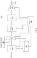
- FIG 2 is an illustration of an example transmitter 200, which may be used in the embodiment of Figure 1 .
- chip 110 of Figure 1 may include multiple transmitters the same as or similar to transmitter 200, each of the transmitters transmitting data over one of the conductive lines of the link 130 to a respective receiver at chip 120.
- Figure 2 illustrates one transmitter 200, and it is understood that the other transmitters on a chip may operate in the same or similar manner.
- Transmitter 200 includes FIFO 201, which receives data in a parallel format from upstream logic (not shown).
- FIFO 201 sends its data to multiplexor 202.
- Multiplexor 202 selects between the data it receives from FIFO 201 and bits from pattern generator 203.
- the multiplexor 202 is controlled by upper-level logic 207, which may include a transmitter control module.
- upper-level logic 207 which may include a transmitter control module.
- serializer 204 Assuming that the system data, as opposed to the generated pattern, is output from multiplexor 202, the data is received by serializer 204, which changes the data from a parallel format into a serial format.
- the data in parallel format is eight bits wide, and the serializer generates a single serialized output. Accordingly, the system clock that provides timing for FIFO 201 and multiplexor 202 may operate at a slower rate than the serializer clock that causes the data to be output at eight times the speed.
- the scope of embodiments is not limited to any particular width for parallel data, nor any particular clock speed.
- serializer 204 outputs the serialized data at some multiple clock rate corresponding to a width of the parallel format data.
- the serialized data is received by feed forward equalization (FFE) module 205, which reshapes the data according to an adaptive algorithm to compensate for any expected signal distortion that may be experienced on the conductive line 209.
- FFE feed forward equalization
- Driver 206 may include a latch that is clocked to launch the data and one or more amplifiers to provide an appropriate gain to the data as it is placed on the conductive line 209.
- conductive line 209 may correspond to one of the conductive lines of link 130 of Figure 1 .
- Upper-level logic 207 includes hardware and/or software logic to determine when to put transmitter 200 into a low-power mode and when to exit the low-power mode to return to an active mode. In this example, upper-level logic 207 monitors FIFO 201 to determine when to enter and exit the low-power mode. For instance, if upper-level logic 207 determines that FIFO 201 is empty of system data, then upper-level logic 207 may determine that it is appropriate to enter into a low-power mode. Similarly, in another example, upper-level logic 207 may discern that the data line into FIFO 201 has been idle for a pre-programmed period of time and determine that it is appropriate to enter into the low-power mode.
- upper-level logic 207 when the transmitter 200 is in the low-power mode, it may be appropriate to exit the low-power mode and go back to an active mode once there is system data to transmit. For instance, upper-level logic 207 may monitor FIFO 201 and may determine to exit the low-power mode when it loads system data and/or may monitor the data line into FIFO 201 to determine to exit the low-power mode when system data is fed into FIFO 201.
- Upper-level logic 207 also communicates with clock module 208 to cause clock module 208 to reduce a clock rate that is applied to transmitter 200. Specifically, in this example, the reduced clock may be applied to the serializer 204, FFE 205, and driver 206 to transmit serialized data bits at the lower clock rate during the low-power mode. During the active mode, though, upper-level logic 207 may control clock module 208 to provide a clock at a normal rate. An example clock module 208 is described in more detail with respect to Figure 4 .
- Multiplexor 202 selects between the data pattern from pattern generator 203 and the system data from FIFO 201, so that the data output from multiplexor 202 is from one of those two sources at any given time.
- upper-level logic 207 causes multiplexor 202 to select system data from FIFO 201 during active mode and to select the data pattern from pattern generator 203 during the low-power mode. Further in this example, upper-level logic 207 may send a control signal to multiplexor 202 to cause multiplexor 202 to select one of those inputs.
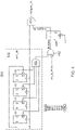
- Figure 3 is an illustration of an example receiver 300, which may be included in a chip-to-chip interface such as that shown in Figure 1 .
- chip 120 may include multiple receivers the same as or similar to receiver 300 configured to receive data over links 130 from chip 110.
- Figure 3 illustrates one receiver 300, and it is understood that a chip-to-chip interface may have multiple receivers, each of the receivers corresponding to a conductive line of links 130.
- conductive line 209 carries serialized data that is either system data or originates from pattern generator 203.
- Variable gain amplifier 301 adjusts a gain of the received data before it passes the data to latches 302.
- Latches 302 output the serialized data to deserializer 303.
- Deserializer 303 de-serializes the data and passes the data further onto pattern checker 305 and to FIFO data buffer 306.
- Figure 3 omits further downstream components for ease of illustration.
- Upper-level logic 307 such as a receiver controller module, includes hardware or software logic to determine when the transmitter enters or exits a low-power mode and to take appropriate action. For instance, upper-level logic 307 monitors conductive line 209 to receive command signals from upper-level logic 207 at the transmitter and to act in response to those command signals.
- upper-level logic 307 receives a first command signal indicating that the transmitter is entering a low-power mode. Accordingly, the upper-level logic 307 then sends a control signal to variable gain amplifier 301 to cause variable gain amplifier 301 to halt performing adaptive variable gain control and to save its variable gain control settings. In response, the variable gain amplifier 301 applies the current variable gain control settings without adaptively varying the gain until upper-level logic 307 indicates otherwise.
- Upper-level logic 307 may include memory to save the variable gain control settings, or those gain control settings may be saved at variable gain controller 301 or some other appropriate place.
- upper-level logic 307 receives an additional command signal indicating that the transmitter is subsequently exiting the low-power mode. In response, the upper-level logic 307 sends another control signal to the variable gain amplifier 301 to cause the variable gain amplifier 301 to resume adaptively performing automatic gain control. In response, variable gain amplifier 301 accesses the saved gain control settings and applies them as a starting value as it resumes its adaptive algorithm.
- upper-level logic 307 in response to receiving the command signal indicating that the transmitter is entering the low-power mode, it sends one or more control signals to clock and data recovery (CDR) and equalization (EQ) component 304 to cause the equalization circuits to halt adaptively performing equalization.
- the equalization circuits save a current equalization setting either at upper-level logic 307 or at another appropriate place and to continue performing equalization, although not adaptively. Rather, during low-power mode, the equalization circuits apply the saved equalization settings.
- upper-level logic 307 When upper-level logic 307 receives an additional command signal indicating that the transmitter is subsequently exiting the low-power mode, upper-level logic 307 sends another control signal to CDR and EQ 304 to cause equalization circuits to resume adaptively performing equalization. In response, the equalization circuits access the saved equalization settings and apply them as a starting value as it resumes its adaptive algorithm.
- the CDR circuits at component 304 in this example receive the data and perform phase interpolation adaptively to keep either the leading edge or the falling edge of the received data within a particular window of allowed phase values relative to a clock to ensure that latches 302 can properly sample the data.
- the CDR circuits may adaptively adjust a phase locked loop (not shown), thereby adjusting the clock that is applied to latches 302 to maintain the phase lock on the data.
- the CDR circuits at component 304 continue to perform clock and data recovery to maintain a phase lock on the data during the low-power mode. Accordingly, the CDR circuits continue to adaptively adjust the phase locked loop to maintain phase lock both before, during, and after the low-power mode.
- FIG 4 is an illustration of an example clock module 208 ( Figure 2 ), according to one embodiment.
- the example clock module 208 of Figure 4 is operable to provide an undivided clock (clk) and a clock that is divided by eight (div8gate_clk).
- clk undivided clock
- clk a clock that is divided by eight
- divide_clk any appropriate amount, such as 2, 4, 16, etc., by increasing or reducing a number of flip-flops.
- the clock module 208 of Figure 4 includes a Johnson counter 410, which has four flip-flops Q0-Q4.
- the undivided clock (clk) is shown in Figure 5 .
- the output of flip-flop Q3 is shown as div8_clk, which is divided by eight relative to clk, although the pulses are wider.
- the outputs of each of the flip-flops Q0-Q4 are input to AND gate 401.
- the particular Johnson counter 410 of Figure 4 is configured so that its output from AND gate 401 is a two-bit wide pulse occurring when the inputs to AND gate 401 are 1000.
- the scope of embodiments is not limited to that particular configuration, as any combination of binary ones and zeros at the output of flip-flops Q0-Q3 may be chosen to cause the two-bit wide pulse.
- the output of AND gate 401 is one of the inputs to OR gate 402, where the set_lp_mode signal acts as an enable.
- upper-level logic 207 may provide set_lp_mode to clock module 208 to cause clock module 208 to output either a divided (div8gate_clk) or an undivided (elk) clock.
- set_lp_mode when set_lp_mode has a value of one, it causes clock module 208 to output the divided clock (div8gate_clk) and when set_lp_mode has a value of zero it causes clock module 208 to output the undivided clock (clk).
- the output of AND gate 404 is either the divided clock or the undivided clock.
- Flip-flop 403 is a negative clock edge flop, and it delays the div8gate signal by half a cycle.
- the output of flip-flop 403 is input to AND gate 404, so that the resulting divided by eight clock looks like that shown in Figure 5 (div8gate_clk).
- div8gate_clk has the same pulse width as the undivided clock clk, and the rising edge of the pulse of div8gate_clk has minimal or no perceptible phase shift from the undivided clock clk. This is illustrated by dashed line 501.
- the divided clock div8gate_clk since the divided clock div8gate_clk has a same phase as the undivided clock clk, it causes the transmitter to transmit the data also having a same phase, and this allows the receiver to maintain a phase lock on the data even during low-power mode.
- Figure 6 is an illustration of method 600 for entering and exiting a low-power mode.
- the method 600 is performed by a transmitter and receiver, such as the example transmitter 200 and Figure 2 and example receiver 300 Figure 3 .
- Requester Ctrl may correspond to upper-level logic 207 ( Figure 2 ) and Responder Ctrl may correspond to upper-level logic 307 ( Figure 3 ).
- the Requester Phy may correspond to a serializer 204, FFE 205, and driver 206, whereas Responder Phy may correspond to the VGA 301, latches 302, and deserializer 303.
- upper-level logic (e.g., logic 207 or logic 307) includes processing circuitry that executes computer readable instructions to determine when to enter or exit a low-power mode and when to perform other appropriate actions in response to either entering or exiting the low-power mode.
- the upper-level logic 207 or 307 may include hardware and/or software to perform the functionality described in Figures 6 and 7 .
- the transmitter and receiver combination is operating according to the active mode.
- the active mode includes operating at the normal clock frequency clk and passing system data from the transmitter to the receiver over a high-speed serial link.
- the Requester Ctrl determines that it is appropriate to enter into a low-power mode, so it sends a command signal (LP_REQ) to the Responder Ctrl.
- the command signal be in any particular format, such as a 128 bit command signal for which the Responder Ctrl is programmed to recognize.
- the Responder CTRL receives the command signal and determines that the transmitter is entering the low-power mode. Accordingly, the Responder CTRL causes the receiver to halt performing adaptive gain control and equalization on the received data at actions 606 and 610. As noted above, the receiver saves its gain control and equalization settings and continues to use the same equalization and gain control settings outside of an adaptive control loop during the low-power mode. Also, at actions 608 and 610 the Responder CTRL is no longer looking for system data, instead examining the data input for an additional command signal from the transmitter to indicate that the transmitter is exiting the low-power mode.
- the Requester CTRL asserts the set_lp_mode signal, thereby causing the transmitter clock module to begin clock division.
- the clock divides by eight during the low-power mode, although other embodiments may use different clock division factors.
- the transmitter is in low-power mode. As described in the examples above, low-power mode may include both operating at a divided clock rate and transmitting a preprogrammed pattern for data, such as 1010, instead of system data.
- both the receiver and the transmitter are operating in a low-power mode.
- this may include operating at a lower clock rate and providing preprogrammed bit patterns as data at the lower clock rate, whereas on the receive side it includes halting adaptive variable gain and equalization operations while continuing to maintain phase lock on the data.
- the transmitter and receiver continue in the low-power mode until the upper-level logic determines that it is appropriate to exit the low-power mode.
- the Requester CTRL de-asserts the set_lp_mode signal in response to determining that it is appropriate to exit the low-power mode. For instance, as described above, the upper-level logic may monitor a transmitter FIFO or a data input line and determine that there is system data to be transmitted. Accordingly, the upper-level logic may then determine to exit the low-power mode by de-asserting the set_lp_mode signal. In response, the clock module provides the undivided clock to the Requester Phy, which then sends data over the link to the receiver at the undivided clock rate, and the transmitter is in normal mode at action 618.
- the transmitter causes the multiplexer to select the input from the FIFO rather than the preprogrammed pattern generator bits.
- the FIFO may send dummy data during this period to allow the receiver time to detect the next command signal and to resume its adaptive variable gain and equalization algorithms.
- the Requester CTRL sends an additional command signal (LP_EXIT) to the Responder CTRL to instruct the receiver to exit the low-power mode.
- the Responder CTRL recognizes the command signal, and in response to the command signal de-asserts the halt_training signal at action 624 and resumes training on data at action 626.
- action 626 includes resuming adaptively performing variable gain control and equalization by applying the saved variable gain and equalization settings. Note that at this point, the receiver has been maintaining a phase lock on the data throughout the low-power mode, so in the present invention, the system is benefited by saving any time that would otherwise have been used to establish phase lock.
- the transmitter may at this point transmit system data over the link to the receiver, and the receiver after action 626 is in full active mode 628. Accordingly, the receiver latches, equalizes, and sends the system data on to downstream components.
- the data entering the FIFO may be scrambled so that selection by the multiplexor of either the pattern bits or the FIFO input necessarily chooses between scrambled or non-scrambled data. Accordingly, during normal operating mode (e.g., active mode) the receiver may see data that otherwise appears random due to the scrambling, whereas beginning at action 614, the receiver may see the preprogrammed data that is a repeating pattern rather than pseudorandom. Examples of scrambling may include, but are not limited to, coding such as 8b10b. Then once again at action 618, the data may begin to appear random as the multiplexor selects the FIFO data input.
- Figure 7 is an illustration of a method 700 for entering and exiting low-power mode by a chip-to-chip interface, according to the present invention.
- the actions of method 700 may be performed for example by the upper-level logic 207, 307 of Figures 2 and 3 as a chip-to-chip interface determines to enter low-power mode and exit low-power mode.
- the upper-level logic may provide such functionality by executing computer readable instructions from computer readable media, and the upper-level logic may be implemented using hardware and/or software.
- the transmitter transmits data signals to a receiver over a high-speed serial data link during a first mode of operation.
- the first mode of operation may include, e.g., operating in a first clock rate and sending system data over the chip-to-chip link.
- the system data may include scrambled data from a transmitter FIFO buffer.
- Action 710 may also include monitoring a data buffer, such as a FIFO buffer, at the transmit side for system data. On the receive side, the receiver performs adaptive variable gain control, adaptive equalization, and maintains a phase lock on the data.
- the upper-level logic of the transmitter side causes the transmitter to enter a low-power mode of operation in response to monitoring data transmission during the first mode of operation.
- the upper-level logic may monitor the data transmission and determine that the data buffer is empty of data or that there is no system data or little system data at the input to the FIFO data buffer.
- the upper-level logic determines to enter the low power mode in response to determining that the data buffer is empty data or that there is no system data or little system data at the input to the data buffer.
- various embodiments may use any appropriate criteria to determine that low-power mode should be entered.
- the upper-level logic causes the clock module at the transmitter to assume the divided operation with a same phase alignment as during the first mode of operation. Examples are shown above, wherein the undivided clock clk is used during active mode or normal mode, and the divided clock div8gate_clk is used during the low-power mode. Whether the transmitter uses its active mode clock or its divided clock, the clock triggers data to be sent over the serial link to the receiver.
- Actions 720 and 730 also includes sending a first command signal from the transmitter to the receiver over the link, wherein the first command signal indicates that the transmitter is entering the low-power mode.
- the receiver halts performance of equalization and variable gain control and saves equalization and variable gain control settings.
- the receiver maintains a phase lock on the data signals during the low-power mode of operation. As noted above, the receiver maintains a phase lock also during the first mode of operation as well. In the examples above, the receiver maintains the phase lock by performing CDR on the received data and adjusting a phase locked loop to clock a latch so that the data is latched on the receive side within a particular phase window.
- the upper-level logic at the transmitter exits the low-power mode of operation in response to monitoring data transmission.
- the upper-level logic of the transmitter may monitor a FIFO data buffer or a data line in and determine that system data is being received and should be transmitted on the data link.
- the upper-level logic at the transmitter may determine that the FIFO buffer at the transmitter includes data and may then send a second command signal to the receiver, wherein the second command signal indicates that the transmitter is exiting low-power mode.
- the receiver resumes performance of equalization and variable gain control by applying the saved equalization and variable gain control settings.
- the upper-level logic of the transmitter may then resume using the active mode clock, e.g., an undivided clock.
- the transmitter may switch to transmitting system data as it exits the low-power mode in interest the active mode.
- method 700 may include entering and exiting low-power mode multiple times during operation of a device by repeating actions 710-750 as system data is either available are not available for transmitting on the transmitter side.
- Various embodiments may include one or more advantages over conventional solutions. For instance, while some conventional solutions may turn the receiver side off or partly off, various example embodiments described herein may leave the receiver on just enough to maintain CDR lock. Specifically, various example embodiments described herein may maintain a phase lock on data at the receiver side, thereby reducing or eliminating time that would otherwise be used to regain a phase lock on the receiver side during exit of the low-power mode. Such embodiments may save some power at the receiver side by halting activities, such as adaptive gain control and adaptive equalization.
- various embodiments may divide a clock frequency during low-power mode of the transmitter, and the act of dividing the clock frequency may result in power savings at the clock tree on the transmitter side because fewer bits are being latched and driven per unit time. Additionally, various embodiments that select between an active mode clock and a divided clock may see reduced exit time because the clock gating mechanism (e.g., as noted above with respect to Figures 4 and 5 ) may add negligible time to the exit process. This is in contrast to some conventional solutions that may turn off transmitters or receivers altogether and may therefore use more exit time.
Landscapes
- Engineering & Computer Science (AREA)
- Theoretical Computer Science (AREA)
- Physics & Mathematics (AREA)
- General Engineering & Computer Science (AREA)
- General Physics & Mathematics (AREA)
- Computer Networks & Wireless Communication (AREA)
- Signal Processing (AREA)
- Dc Digital Transmission (AREA)
- Information Transfer Systems (AREA)
- Synchronisation In Digital Transmission Systems (AREA)
- Power Sources (AREA)
Claims (10)
- Système (100) comprenant :un émetteur (200) couplé à une liaison (130) ;un récepteur (300) couplé à la liaison et configuré pour recevoir des signaux sur la liaison en provenance de l'émetteur ;un module de commande d'émission (207) configuré pour amener l'émetteur à entrer et à sortir d'un mode basse consommation ; etun module d'horloge (208) couplé à l'émetteur et configuré pour fournir un signal d'horloge à l'émetteur, dans lequel le module d'horloge (208) est en outre configuré pour fournir le signal d'horloge en tant que signal d'horloge divisé à l'émetteur (200) lorsque l'émetteur (200) est en mode basse consommation, dans lequel en outre le signal d'horloge divisé a une même phase que le signal d'horloge avant l'entrée dans le mode basse consommation ;dans lequel le récepteur (300) est configuré pour arrêter l'exécution d'une égalisation adaptative et d'une commande de gain variable en réponse à l'entrée de l'émetteur dans le mode basse consommation ;caractérisé en ce quele récepteur (300) est en outre configuré pour enregistrer des réglages de commande de gain variable et des réglages d'égalisation en réponse à l'entrée de l'émetteur (200) dans le mode basse consommation ; etdans lequel le récepteur (300) est en outre configuré pour reprendre l'exécution de l'égalisation adaptative et de la commande de gain variable, en réponse à la sortie ultérieure de l'émetteur (200) du mode basse consommation, en appliquant les réglages de commande de gain variable et les réglages d'égalisation sauvegardés.
- Système (100) selon la revendication 1, dans lequel la liaison (130) comprend une liaison de données série à haut débit entre l'émetteur (200) et le récepteur (300).
- Système (100) selon la revendication 2, dans lequel la liaison (130) comprend une liaison puce à puce, et dans lequel l'émetteur (200) est disposé sur une première puce semiconductrice (110) et le récepteur (300) est disposé sur une deuxième puce semiconductrice (120).
- Système (100) selon la revendication 1, dans lequel le récepteur (300) est configuré pour rester allumé pendant le mode basse consommation et pendant un mode actif.
- Système (100) selon la revendication 1, dans lequel le récepteur (300) est configuré pour rester verrouillé en phase sur un signal de données provenant de l'émetteur (200) pendant le mode basse consommation.
- Procédé (700) comprenant :l'émission (710) de signaux de données provenant d'un émetteur (200) à un récepteur (300) sur une liaison de données en série pendant un premier mode de fonctionnement ;l'entrée forcée (720) de l'émetteur dans un mode de fonctionnement à basse consommation en réponse à la surveillance de l'émission de données pendant le premier mode de fonctionnement ;en réponse à l'entrée dans le mode de fonctionnement à basse consommation, la prise forcée (730) par un module d'horloge (208) au niveau de l'émetteur (200) d'un fonctionnement divisé avec un même alignement de phase que pendant le premier mode de fonctionnement ; etle maintien (740) d'un verrouillage de phase sur les signaux de données par le récepteur pendant le premier mode de fonctionnement et pendant le mode de fonctionnement à basse consommation ;l'envoi un premier signal de commande depuis l'émetteur (200) au récepteur sur la liaison série ;en réponse à la réception du premier signal de commande, l'arrêt d'une égalisation adaptative et d'une commande de gain variable au niveau du récepteur (300) ;caractérisé en ce que :en réponse à la réception du premier signal de commande, l'enregistrement de réglages de commande de gain variable et d'égalisation ;l'envoi d'un deuxième signal de commande depuis l'émetteur au récepteur sur la liaison série ; eten réponse à la réception du deuxième signal de commande, la reprise de l'égalisation adaptative et de la commande de gain variable au niveau du récepteur en appliquant les réglages de commande de gain variable et les réglages d'égalisation sauvegardés.
- Procédé (700) selon la revendication 6, dans lequel les signaux de données comprennent un ensemble répétitif de bits numériques pendant le mode de fonctionnement à basse consommation.
- Procédé (700) selon la revendication 6, dans lequel les signaux de données comprennent des données brouillées pendant le premier mode de fonctionnement.
- Procédé (700) selon la revendication 6, comprenant en outre :la surveillance d'un tampon de données premier entré, premier sorti, FIFO, au niveau de l'émetteur pour déterminer que le tampon de données FIFO est vide de données ; etla détermination d'entrer dans le mode de fonctionnement à basse consommation en réponse à la détermination que le tampon de données FIFO est vide de données.
- Procédé (700) selon la revendication 6, comprenant en outre :
après l'entrée dans le mode de fonctionnement à basse consommation, la sortie du mode de fonctionnement à basse consommation en réponse à la détermination qu'un tampon de données premier entré premier sorti, FIFO, au niveau de l'émetteur comporte des données.
Applications Claiming Priority (2)
| Application Number | Priority Date | Filing Date | Title |
|---|---|---|---|
| US15/666,764 US10218391B1 (en) | 2017-08-02 | 2017-08-02 | Systems and methods providing a low-power mode for serial links |
| PCT/US2018/038065 WO2019027581A1 (fr) | 2017-08-02 | 2018-06-18 | Systèmes et procédés fournissant un mode de faible puissance pour des liaisons série |
Publications (2)
| Publication Number | Publication Date |
|---|---|
| EP3662349A1 EP3662349A1 (fr) | 2020-06-10 |
| EP3662349B1 true EP3662349B1 (fr) | 2022-10-05 |
Family
ID=62842316
Family Applications (1)
| Application Number | Title | Priority Date | Filing Date |
|---|---|---|---|
| EP18738162.9A Active EP3662349B1 (fr) | 2017-08-02 | 2018-06-18 | Systèmes et procédés fournissant un mode de faible puissance pour des liaisons série |
Country Status (5)
| Country | Link |
|---|---|
| US (1) | US10218391B1 (fr) |
| EP (1) | EP3662349B1 (fr) |
| CN (1) | CN110998485B (fr) |
| TW (1) | TWI676888B (fr) |
| WO (1) | WO2019027581A1 (fr) |
Families Citing this family (4)
| Publication number | Priority date | Publication date | Assignee | Title |
|---|---|---|---|---|
| KR102915782B1 (ko) * | 2021-12-24 | 2026-01-20 | 엘지디스플레이 주식회사 | 표시장치 |
| CN116414755A (zh) | 2021-12-31 | 2023-07-11 | 华为技术有限公司 | 一种高速串行接口和数据传输方法 |
| US12130758B2 (en) * | 2022-08-24 | 2024-10-29 | Qualcomm Incorporated | Data transmission power optimization |
| US12519608B2 (en) * | 2023-10-23 | 2026-01-06 | Nvidia Corp. | Adaptive clock generation for serial links |
Family Cites Families (22)
| Publication number | Priority date | Publication date | Assignee | Title |
|---|---|---|---|---|
| US6819150B1 (en) | 2001-09-19 | 2004-11-16 | Sony Corporation | Method and apparatus for quick clock swapping using much slower asynchronous clock for power savings |
| EP2375662B1 (fr) * | 2005-01-20 | 2018-09-26 | Rambus Inc. | Systemes de signalisation a grande vitesse a egalisation et preaccentuation adaptables |
| US7352248B2 (en) | 2005-03-01 | 2008-04-01 | Seiko Epson Corporation | Method and apparatus for maintaining a clock/data recovery circuit frequency during transmitter low power mode |
| US7752476B2 (en) | 2006-05-17 | 2010-07-06 | Advanced Micro Devices, Inc. | Fast transition from low-speed mode to high-speed mode in high-speed interfaces |
| US7849339B2 (en) * | 2007-03-23 | 2010-12-07 | Silicon Image, Inc. | Power-saving clocking technique |
| JP2009026047A (ja) * | 2007-07-19 | 2009-02-05 | Nec Electronics Corp | 動作周波数動的自動制御機能を有するオーディオプロセッサ |
| CN100487716C (zh) * | 2007-07-20 | 2009-05-13 | 深圳兆日技术有限公司 | 一种相位对准装置、应用该装置的设备及方法 |
| WO2010080172A1 (fr) * | 2009-01-12 | 2010-07-15 | Rambus Inc. | Système de signalisation de faible puissance à transfert d'horloge |
| WO2012021380A2 (fr) | 2010-08-13 | 2012-02-16 | Rambus Inc. | Mémoire d'éveil rapide |
| WO2012049815A1 (fr) * | 2010-10-12 | 2012-04-19 | パナソニック株式会社 | Circuit d'émission, circuit de réception, procédé d'émission, procédé de réception, système de communication et procédé de communication s'y rapportant |
| US8578222B2 (en) * | 2011-02-17 | 2013-11-05 | Qualcomm Incorporated | SerDes power throttling as a function of detected error rate |
| US8923087B2 (en) | 2012-01-19 | 2014-12-30 | Lsi Corporation | Method and apparatus for decreasing leakage power consumption in power gated memories |
| US9117036B2 (en) * | 2012-09-26 | 2015-08-25 | Ati Technologies Ulc | Fast exit from low-power state for bus protocol compatible device |
| US9600431B2 (en) | 2012-10-22 | 2017-03-21 | Intel Corporation | High performance interconnect physical layer |
| US8837561B2 (en) * | 2012-11-21 | 2014-09-16 | Texas Instruments Incorporated | Initialization sequence for bi-directional communications in a carrier-based system |
| CN104301121A (zh) * | 2013-07-19 | 2015-01-21 | 中兴通讯股份有限公司 | 一种控制方法、装置及光收发器 |
| US9467120B1 (en) | 2013-12-19 | 2016-10-11 | Altera Corporation | Power management for PCI express |
| US9552322B2 (en) * | 2014-06-12 | 2017-01-24 | Pericom Semiconductor Corporation | Hybrid repeater for supporting backward compatibility |
| US9792247B2 (en) * | 2014-07-18 | 2017-10-17 | Qualcomm Incorporated | Systems and methods for chip to chip communication |
| JP6354553B2 (ja) * | 2014-12-02 | 2018-07-11 | 住友電気工業株式会社 | バイアス制御回路およびそれを含む光送信器 |
| JP2018506915A (ja) * | 2015-02-04 | 2018-03-08 | クアルコム,インコーポレイテッド | データリンク電力低減およびスループット向上のためのマルチ変調 |
| US10007319B2 (en) * | 2015-12-17 | 2018-06-26 | Microsemi Solutions (U.S.), Inc. | Power saving in multi-directional data transfer |
-
2017
- 2017-08-02 US US15/666,764 patent/US10218391B1/en active Active
-
2018
- 2018-06-18 WO PCT/US2018/038065 patent/WO2019027581A1/fr not_active Ceased
- 2018-06-18 CN CN201880050674.9A patent/CN110998485B/zh active Active
- 2018-06-18 EP EP18738162.9A patent/EP3662349B1/fr active Active
- 2018-06-21 TW TW107121347A patent/TWI676888B/zh active
Also Published As
| Publication number | Publication date |
|---|---|
| EP3662349A1 (fr) | 2020-06-10 |
| WO2019027581A1 (fr) | 2019-02-07 |
| US20190044553A1 (en) | 2019-02-07 |
| US10218391B1 (en) | 2019-02-26 |
| CN110998485B (zh) | 2023-08-25 |
| TWI676888B (zh) | 2019-11-11 |
| CN110998485A (zh) | 2020-04-10 |
| TW201910970A (zh) | 2019-03-16 |
Similar Documents
| Publication | Publication Date | Title |
|---|---|---|
| US5621774A (en) | Method and apparatus for synchronizing parallel data transfer | |
| US5794020A (en) | Data transfer apparatus fetching reception data at maximum margin of timing | |
| EP3662349B1 (fr) | Systèmes et procédés fournissant un mode de faible puissance pour des liaisons série | |
| US9355054B2 (en) | Digital calibration-based skew cancellation for long-reach MIPI D-PHY serial links | |
| US5793227A (en) | Synchronizing logic avoiding metastability | |
| US8595541B2 (en) | Data processing modules requiring different average clock frequencies having a common clock and a clock gating circuit for deleting clock pulses applied to the modules at times consistent with data sourcing and sinking capabilities | |
| KR100866601B1 (ko) | 반도체 장치의 종단 저항을 제어할 수 있는 장치 및 방법 | |
| US20160071563A1 (en) | Output timing control circuit of semiconductor apparatus and method thereof | |
| CN103003882B (zh) | 用于源同步信息传送的装置和关联方法 | |
| US6424688B1 (en) | Method to transfer data in a system with multiple clock domains using clock skipping techniques | |
| US12267075B2 (en) | Low-power inter-die communication using delay lines | |
| US11870615B2 (en) | Summing circuit and equalizer including the same | |
| US7512201B2 (en) | Multi-channel synchronization architecture | |
| JPWO2009014182A1 (ja) | データ転送装置およびデータ転送方法 | |
| KR100894486B1 (ko) | 디지털 필터, 클록 데이터 복구 회로 및 그 동작방법, 반도체 메모리 장치 및 그의 동작방법 | |
| US7734944B2 (en) | Mechanism for windaging of a double rate driver | |
| US7934109B2 (en) | Low power mode unipolar current/voltage mode interface | |
| US6760392B1 (en) | Method and apparatus to provide fixed latency early response in a system with multiple clock domains with fixable clock ratios | |
| US11018904B1 (en) | Equalization for a transmitter circuit | |
| US7249273B2 (en) | Synchronized serial interface | |
| US7711940B2 (en) | Circuit block and circuit system having skew compensation, and skew compensation method | |
| CN100454803C (zh) | 一种快速无毛刺的时钟倒换方法和装置 | |
| US20260039514A1 (en) | Decision feedback equalizer for double data rate memory | |
| US20260121822A1 (en) | Device for performing device-to-device communication based on high-speed serial interface and operating method thereof | |
| US6647507B1 (en) | Method for improving a timing margin in an integrated circuit by setting a relative phase of receive/transmit and distributed clock signals |
Legal Events
| Date | Code | Title | Description |
|---|---|---|---|
| STAA | Information on the status of an ep patent application or granted ep patent |
Free format text: STATUS: UNKNOWN |
|
| STAA | Information on the status of an ep patent application or granted ep patent |
Free format text: STATUS: THE INTERNATIONAL PUBLICATION HAS BEEN MADE |
|
| PUAI | Public reference made under article 153(3) epc to a published international application that has entered the european phase |
Free format text: ORIGINAL CODE: 0009012 |
|
| STAA | Information on the status of an ep patent application or granted ep patent |
Free format text: STATUS: REQUEST FOR EXAMINATION WAS MADE |
|
| 17P | Request for examination filed |
Effective date: 20191218 |
|
| AK | Designated contracting states |
Kind code of ref document: A1 Designated state(s): AL AT BE BG CH CY CZ DE DK EE ES FI FR GB GR HR HU IE IS IT LI LT LU LV MC MK MT NL NO PL PT RO RS SE SI SK SM TR |
|
| AX | Request for extension of the european patent |
Extension state: BA ME |
|
| DAV | Request for validation of the european patent (deleted) | ||
| DAX | Request for extension of the european patent (deleted) | ||
| STAA | Information on the status of an ep patent application or granted ep patent |
Free format text: STATUS: EXAMINATION IS IN PROGRESS |
|
| 17Q | First examination report despatched |
Effective date: 20210311 |
|
| REG | Reference to a national code |
Ref country code: DE Ref legal event code: R079 Ref document number: 602018041401 Country of ref document: DE Free format text: PREVIOUS MAIN CLASS: G06F0001320000 Ipc: G06F0001323400 |
|
| GRAP | Despatch of communication of intention to grant a patent |
Free format text: ORIGINAL CODE: EPIDOSNIGR1 |
|
| STAA | Information on the status of an ep patent application or granted ep patent |
Free format text: STATUS: GRANT OF PATENT IS INTENDED |
|
| RIC1 | Information provided on ipc code assigned before grant |
Ipc: G06F 13/42 20060101ALI20220405BHEP Ipc: G06F 1/08 20060101ALI20220405BHEP Ipc: G06F 1/3228 20190101ALI20220405BHEP Ipc: G06F 1/324 20190101ALI20220405BHEP Ipc: G06F 1/3234 20190101AFI20220405BHEP |
|
| INTG | Intention to grant announced |
Effective date: 20220428 |
|
| GRAS | Grant fee paid |
Free format text: ORIGINAL CODE: EPIDOSNIGR3 |
|
| GRAA | (expected) grant |
Free format text: ORIGINAL CODE: 0009210 |
|
| STAA | Information on the status of an ep patent application or granted ep patent |
Free format text: STATUS: THE PATENT HAS BEEN GRANTED |
|
| AK | Designated contracting states |
Kind code of ref document: B1 Designated state(s): AL AT BE BG CH CY CZ DE DK EE ES FI FR GB GR HR HU IE IS IT LI LT LU LV MC MK MT NL NO PL PT RO RS SE SI SK SM TR |
|
| REG | Reference to a national code |
Ref country code: GB Ref legal event code: FG4D |
|
| REG | Reference to a national code |
Ref country code: CH Ref legal event code: EP |
|
| REG | Reference to a national code |
Ref country code: AT Ref legal event code: REF Ref document number: 1523146 Country of ref document: AT Kind code of ref document: T Effective date: 20221015 |
|
| REG | Reference to a national code |
Ref country code: DE Ref legal event code: R096 Ref document number: 602018041401 Country of ref document: DE |
|
| REG | Reference to a national code |
Ref country code: IE Ref legal event code: FG4D |
|
| REG | Reference to a national code |
Ref country code: LT Ref legal event code: MG9D |
|
| REG | Reference to a national code |
Ref country code: NL Ref legal event code: MP Effective date: 20221005 |
|
| REG | Reference to a national code |
Ref country code: AT Ref legal event code: MK05 Ref document number: 1523146 Country of ref document: AT Kind code of ref document: T Effective date: 20221005 |
|
| PG25 | Lapsed in a contracting state [announced via postgrant information from national office to epo] |
Ref country code: NL Free format text: LAPSE BECAUSE OF FAILURE TO SUBMIT A TRANSLATION OF THE DESCRIPTION OR TO PAY THE FEE WITHIN THE PRESCRIBED TIME-LIMIT Effective date: 20221005 |
|
| PG25 | Lapsed in a contracting state [announced via postgrant information from national office to epo] |
Ref country code: SE Free format text: LAPSE BECAUSE OF FAILURE TO SUBMIT A TRANSLATION OF THE DESCRIPTION OR TO PAY THE FEE WITHIN THE PRESCRIBED TIME-LIMIT Effective date: 20221005 Ref country code: PT Free format text: LAPSE BECAUSE OF FAILURE TO SUBMIT A TRANSLATION OF THE DESCRIPTION OR TO PAY THE FEE WITHIN THE PRESCRIBED TIME-LIMIT Effective date: 20230206 Ref country code: NO Free format text: LAPSE BECAUSE OF FAILURE TO SUBMIT A TRANSLATION OF THE DESCRIPTION OR TO PAY THE FEE WITHIN THE PRESCRIBED TIME-LIMIT Effective date: 20230105 Ref country code: LT Free format text: LAPSE BECAUSE OF FAILURE TO SUBMIT A TRANSLATION OF THE DESCRIPTION OR TO PAY THE FEE WITHIN THE PRESCRIBED TIME-LIMIT Effective date: 20221005 Ref country code: FI Free format text: LAPSE BECAUSE OF FAILURE TO SUBMIT A TRANSLATION OF THE DESCRIPTION OR TO PAY THE FEE WITHIN THE PRESCRIBED TIME-LIMIT Effective date: 20221005 Ref country code: ES Free format text: LAPSE BECAUSE OF FAILURE TO SUBMIT A TRANSLATION OF THE DESCRIPTION OR TO PAY THE FEE WITHIN THE PRESCRIBED TIME-LIMIT Effective date: 20221005 Ref country code: AT Free format text: LAPSE BECAUSE OF FAILURE TO SUBMIT A TRANSLATION OF THE DESCRIPTION OR TO PAY THE FEE WITHIN THE PRESCRIBED TIME-LIMIT Effective date: 20221005 |
|
| PG25 | Lapsed in a contracting state [announced via postgrant information from national office to epo] |
Ref country code: RS Free format text: LAPSE BECAUSE OF FAILURE TO SUBMIT A TRANSLATION OF THE DESCRIPTION OR TO PAY THE FEE WITHIN THE PRESCRIBED TIME-LIMIT Effective date: 20221005 Ref country code: PL Free format text: LAPSE BECAUSE OF FAILURE TO SUBMIT A TRANSLATION OF THE DESCRIPTION OR TO PAY THE FEE WITHIN THE PRESCRIBED TIME-LIMIT Effective date: 20221005 Ref country code: LV Free format text: LAPSE BECAUSE OF FAILURE TO SUBMIT A TRANSLATION OF THE DESCRIPTION OR TO PAY THE FEE WITHIN THE PRESCRIBED TIME-LIMIT Effective date: 20221005 Ref country code: IS Free format text: LAPSE BECAUSE OF FAILURE TO SUBMIT A TRANSLATION OF THE DESCRIPTION OR TO PAY THE FEE WITHIN THE PRESCRIBED TIME-LIMIT Effective date: 20230205 Ref country code: HR Free format text: LAPSE BECAUSE OF FAILURE TO SUBMIT A TRANSLATION OF THE DESCRIPTION OR TO PAY THE FEE WITHIN THE PRESCRIBED TIME-LIMIT Effective date: 20221005 Ref country code: GR Free format text: LAPSE BECAUSE OF FAILURE TO SUBMIT A TRANSLATION OF THE DESCRIPTION OR TO PAY THE FEE WITHIN THE PRESCRIBED TIME-LIMIT Effective date: 20230106 |
|
| REG | Reference to a national code |
Ref country code: DE Ref legal event code: R097 Ref document number: 602018041401 Country of ref document: DE |
|
| PG25 | Lapsed in a contracting state [announced via postgrant information from national office to epo] |
Ref country code: SM Free format text: LAPSE BECAUSE OF FAILURE TO SUBMIT A TRANSLATION OF THE DESCRIPTION OR TO PAY THE FEE WITHIN THE PRESCRIBED TIME-LIMIT Effective date: 20221005 Ref country code: RO Free format text: LAPSE BECAUSE OF FAILURE TO SUBMIT A TRANSLATION OF THE DESCRIPTION OR TO PAY THE FEE WITHIN THE PRESCRIBED TIME-LIMIT Effective date: 20221005 Ref country code: EE Free format text: LAPSE BECAUSE OF FAILURE TO SUBMIT A TRANSLATION OF THE DESCRIPTION OR TO PAY THE FEE WITHIN THE PRESCRIBED TIME-LIMIT Effective date: 20221005 Ref country code: DK Free format text: LAPSE BECAUSE OF FAILURE TO SUBMIT A TRANSLATION OF THE DESCRIPTION OR TO PAY THE FEE WITHIN THE PRESCRIBED TIME-LIMIT Effective date: 20221005 Ref country code: CZ Free format text: LAPSE BECAUSE OF FAILURE TO SUBMIT A TRANSLATION OF THE DESCRIPTION OR TO PAY THE FEE WITHIN THE PRESCRIBED TIME-LIMIT Effective date: 20221005 |
|
| PLBE | No opposition filed within time limit |
Free format text: ORIGINAL CODE: 0009261 |
|
| STAA | Information on the status of an ep patent application or granted ep patent |
Free format text: STATUS: NO OPPOSITION FILED WITHIN TIME LIMIT |
|
| PG25 | Lapsed in a contracting state [announced via postgrant information from national office to epo] |
Ref country code: SK Free format text: LAPSE BECAUSE OF FAILURE TO SUBMIT A TRANSLATION OF THE DESCRIPTION OR TO PAY THE FEE WITHIN THE PRESCRIBED TIME-LIMIT Effective date: 20221005 Ref country code: AL Free format text: LAPSE BECAUSE OF FAILURE TO SUBMIT A TRANSLATION OF THE DESCRIPTION OR TO PAY THE FEE WITHIN THE PRESCRIBED TIME-LIMIT Effective date: 20221005 |
|
| 26N | No opposition filed |
Effective date: 20230706 |
|
| PG25 | Lapsed in a contracting state [announced via postgrant information from national office to epo] |
Ref country code: SI Free format text: LAPSE BECAUSE OF FAILURE TO SUBMIT A TRANSLATION OF THE DESCRIPTION OR TO PAY THE FEE WITHIN THE PRESCRIBED TIME-LIMIT Effective date: 20221005 |
|
| PG25 | Lapsed in a contracting state [announced via postgrant information from national office to epo] |
Ref country code: MC Free format text: LAPSE BECAUSE OF FAILURE TO SUBMIT A TRANSLATION OF THE DESCRIPTION OR TO PAY THE FEE WITHIN THE PRESCRIBED TIME-LIMIT Effective date: 20221005 |
|
| PG25 | Lapsed in a contracting state [announced via postgrant information from national office to epo] |
Ref country code: MC Free format text: LAPSE BECAUSE OF FAILURE TO SUBMIT A TRANSLATION OF THE DESCRIPTION OR TO PAY THE FEE WITHIN THE PRESCRIBED TIME-LIMIT Effective date: 20221005 |
|
| REG | Reference to a national code |
Ref country code: CH Ref legal event code: PL |
|
| REG | Reference to a national code |
Ref country code: BE Ref legal event code: MM Effective date: 20230630 |
|
| PG25 | Lapsed in a contracting state [announced via postgrant information from national office to epo] |
Ref country code: LU Free format text: LAPSE BECAUSE OF NON-PAYMENT OF DUE FEES Effective date: 20230618 |
|
| REG | Reference to a national code |
Ref country code: IE Ref legal event code: MM4A |
|
| PG25 | Lapsed in a contracting state [announced via postgrant information from national office to epo] |
Ref country code: LU Free format text: LAPSE BECAUSE OF NON-PAYMENT OF DUE FEES Effective date: 20230618 |
|
| PG25 | Lapsed in a contracting state [announced via postgrant information from national office to epo] |
Ref country code: IE Free format text: LAPSE BECAUSE OF NON-PAYMENT OF DUE FEES Effective date: 20230618 |
|
| PG25 | Lapsed in a contracting state [announced via postgrant information from national office to epo] |
Ref country code: IE Free format text: LAPSE BECAUSE OF NON-PAYMENT OF DUE FEES Effective date: 20230618 Ref country code: CH Free format text: LAPSE BECAUSE OF NON-PAYMENT OF DUE FEES Effective date: 20230630 |
|
| PG25 | Lapsed in a contracting state [announced via postgrant information from national office to epo] |
Ref country code: IT Free format text: LAPSE BECAUSE OF FAILURE TO SUBMIT A TRANSLATION OF THE DESCRIPTION OR TO PAY THE FEE WITHIN THE PRESCRIBED TIME-LIMIT Effective date: 20221005 Ref country code: FR Free format text: LAPSE BECAUSE OF NON-PAYMENT OF DUE FEES Effective date: 20230630 Ref country code: BE Free format text: LAPSE BECAUSE OF NON-PAYMENT OF DUE FEES Effective date: 20230630 |
|
| PGFP | Annual fee paid to national office [announced via postgrant information from national office to epo] |
Ref country code: GB Payment date: 20240509 Year of fee payment: 7 |
|
| PGFP | Annual fee paid to national office [announced via postgrant information from national office to epo] |
Ref country code: DE Payment date: 20240509 Year of fee payment: 7 |
|
| PG25 | Lapsed in a contracting state [announced via postgrant information from national office to epo] |
Ref country code: BG Free format text: LAPSE BECAUSE OF FAILURE TO SUBMIT A TRANSLATION OF THE DESCRIPTION OR TO PAY THE FEE WITHIN THE PRESCRIBED TIME-LIMIT Effective date: 20221005 |
|
| PG25 | Lapsed in a contracting state [announced via postgrant information from national office to epo] |
Ref country code: BG Free format text: LAPSE BECAUSE OF FAILURE TO SUBMIT A TRANSLATION OF THE DESCRIPTION OR TO PAY THE FEE WITHIN THE PRESCRIBED TIME-LIMIT Effective date: 20221005 |
|
| PG25 | Lapsed in a contracting state [announced via postgrant information from national office to epo] |
Ref country code: CY Free format text: LAPSE BECAUSE OF FAILURE TO SUBMIT A TRANSLATION OF THE DESCRIPTION OR TO PAY THE FEE WITHIN THE PRESCRIBED TIME-LIMIT; INVALID AB INITIO Effective date: 20180618 |
|
| PG25 | Lapsed in a contracting state [announced via postgrant information from national office to epo] |
Ref country code: HU Free format text: LAPSE BECAUSE OF FAILURE TO SUBMIT A TRANSLATION OF THE DESCRIPTION OR TO PAY THE FEE WITHIN THE PRESCRIBED TIME-LIMIT; INVALID AB INITIO Effective date: 20180618 |
|
| PG25 | Lapsed in a contracting state [announced via postgrant information from national office to epo] |
Ref country code: TR Free format text: LAPSE BECAUSE OF FAILURE TO SUBMIT A TRANSLATION OF THE DESCRIPTION OR TO PAY THE FEE WITHIN THE PRESCRIBED TIME-LIMIT Effective date: 20221005 |
|
| REG | Reference to a national code |
Ref country code: DE Ref legal event code: R119 Ref document number: 602018041401 Country of ref document: DE |
|
| GBPC | Gb: european patent ceased through non-payment of renewal fee |
Effective date: 20250618 |
|
| PG25 | Lapsed in a contracting state [announced via postgrant information from national office to epo] |
Ref country code: GB Free format text: LAPSE BECAUSE OF NON-PAYMENT OF DUE FEES Effective date: 20250618 |
|
| PG25 | Lapsed in a contracting state [announced via postgrant information from national office to epo] |
Ref country code: DE Free format text: LAPSE BECAUSE OF NON-PAYMENT OF DUE FEES Effective date: 20260101 |