EP3660179A1 - Kompensieren von ablagerungsungleichförmigkeiten in schaltungselementen - Google Patents
Kompensieren von ablagerungsungleichförmigkeiten in schaltungselementen Download PDFInfo
- Publication number
- EP3660179A1 EP3660179A1 EP19212172.1A EP19212172A EP3660179A1 EP 3660179 A1 EP3660179 A1 EP 3660179A1 EP 19212172 A EP19212172 A EP 19212172A EP 3660179 A1 EP3660179 A1 EP 3660179A1
- Authority
- EP
- European Patent Office
- Prior art keywords
- deposition
- mask
- uniformity
- function
- lithography
- Prior art date
- Legal status (The legal status is an assumption and is not a legal conclusion. Google has not performed a legal analysis and makes no representation as to the accuracy of the status listed.)
- Granted
Links
Images



Classifications
-
- G—PHYSICS
- G03—PHOTOGRAPHY; CINEMATOGRAPHY; ANALOGOUS TECHNIQUES USING WAVES OTHER THAN OPTICAL WAVES; ELECTROGRAPHY; HOLOGRAPHY
- G03F—PHOTOMECHANICAL PRODUCTION OF TEXTURED OR PATTERNED SURFACES, e.g. FOR PRINTING, FOR PROCESSING OF SEMICONDUCTOR DEVICES; MATERIALS THEREFOR; ORIGINALS THEREFOR; APPARATUS SPECIALLY ADAPTED THEREFOR
- G03F7/00—Photomechanical, e.g. photolithographic, production of textured or patterned surfaces, e.g. printing surfaces; Materials therefor, e.g. comprising photoresists; Apparatus specially adapted therefor
- G03F7/70—Microphotolithographic exposure; Apparatus therefor
- G03F7/70483—Information management; Active and passive control; Testing; Wafer monitoring, e.g. pattern monitoring
- G03F7/70491—Information management, e.g. software; Active and passive control, e.g. details of controlling exposure processes or exposure tool monitoring processes
-
- G—PHYSICS
- G03—PHOTOGRAPHY; CINEMATOGRAPHY; ANALOGOUS TECHNIQUES USING WAVES OTHER THAN OPTICAL WAVES; ELECTROGRAPHY; HOLOGRAPHY
- G03F—PHOTOMECHANICAL PRODUCTION OF TEXTURED OR PATTERNED SURFACES, e.g. FOR PRINTING, FOR PROCESSING OF SEMICONDUCTOR DEVICES; MATERIALS THEREFOR; ORIGINALS THEREFOR; APPARATUS SPECIALLY ADAPTED THEREFOR
- G03F7/00—Photomechanical, e.g. photolithographic, production of textured or patterned surfaces, e.g. printing surfaces; Materials therefor, e.g. comprising photoresists; Apparatus specially adapted therefor
- G03F7/70—Microphotolithographic exposure; Apparatus therefor
- G03F7/70425—Imaging strategies, e.g. for increasing throughput or resolution, printing product fields larger than the image field or compensating lithography- or non-lithography errors, e.g. proximity correction, mix-and-match, stitching or double patterning
-
- C—CHEMISTRY; METALLURGY
- C23—COATING METALLIC MATERIAL; COATING MATERIAL WITH METALLIC MATERIAL; CHEMICAL SURFACE TREATMENT; DIFFUSION TREATMENT OF METALLIC MATERIAL; COATING BY VACUUM EVAPORATION, BY SPUTTERING, BY ION IMPLANTATION OR BY CHEMICAL VAPOUR DEPOSITION, IN GENERAL; INHIBITING CORROSION OF METALLIC MATERIAL OR INCRUSTATION IN GENERAL
- C23C—COATING METALLIC MATERIAL; COATING MATERIAL WITH METALLIC MATERIAL; SURFACE TREATMENT OF METALLIC MATERIAL BY DIFFUSION INTO THE SURFACE, BY CHEMICAL CONVERSION OR SUBSTITUTION; COATING BY VACUUM EVAPORATION, BY SPUTTERING, BY ION IMPLANTATION OR BY CHEMICAL VAPOUR DEPOSITION, IN GENERAL
- C23C14/00—Coating by vacuum evaporation, by sputtering or by ion implantation of the coating forming material
- C23C14/04—Coating on selected surface areas, e.g. using masks
- C23C14/042—Coating on selected surface areas, e.g. using masks using masks
-
- C—CHEMISTRY; METALLURGY
- C23—COATING METALLIC MATERIAL; COATING MATERIAL WITH METALLIC MATERIAL; CHEMICAL SURFACE TREATMENT; DIFFUSION TREATMENT OF METALLIC MATERIAL; COATING BY VACUUM EVAPORATION, BY SPUTTERING, BY ION IMPLANTATION OR BY CHEMICAL VAPOUR DEPOSITION, IN GENERAL; INHIBITING CORROSION OF METALLIC MATERIAL OR INCRUSTATION IN GENERAL
- C23C—COATING METALLIC MATERIAL; COATING MATERIAL WITH METALLIC MATERIAL; SURFACE TREATMENT OF METALLIC MATERIAL BY DIFFUSION INTO THE SURFACE, BY CHEMICAL CONVERSION OR SUBSTITUTION; COATING BY VACUUM EVAPORATION, BY SPUTTERING, BY ION IMPLANTATION OR BY CHEMICAL VAPOUR DEPOSITION, IN GENERAL
- C23C14/00—Coating by vacuum evaporation, by sputtering or by ion implantation of the coating forming material
- C23C14/06—Coating by vacuum evaporation, by sputtering or by ion implantation of the coating forming material characterised by the coating material
- C23C14/14—Metallic material, boron or silicon
-
- C—CHEMISTRY; METALLURGY
- C23—COATING METALLIC MATERIAL; COATING MATERIAL WITH METALLIC MATERIAL; CHEMICAL SURFACE TREATMENT; DIFFUSION TREATMENT OF METALLIC MATERIAL; COATING BY VACUUM EVAPORATION, BY SPUTTERING, BY ION IMPLANTATION OR BY CHEMICAL VAPOUR DEPOSITION, IN GENERAL; INHIBITING CORROSION OF METALLIC MATERIAL OR INCRUSTATION IN GENERAL
- C23C—COATING METALLIC MATERIAL; COATING MATERIAL WITH METALLIC MATERIAL; SURFACE TREATMENT OF METALLIC MATERIAL BY DIFFUSION INTO THE SURFACE, BY CHEMICAL CONVERSION OR SUBSTITUTION; COATING BY VACUUM EVAPORATION, BY SPUTTERING, BY ION IMPLANTATION OR BY CHEMICAL VAPOUR DEPOSITION, IN GENERAL
- C23C14/00—Coating by vacuum evaporation, by sputtering or by ion implantation of the coating forming material
- C23C14/22—Coating by vacuum evaporation, by sputtering or by ion implantation of the coating forming material characterised by the process of coating
- C23C14/225—Oblique incidence of vaporised material on substrate
-
- C—CHEMISTRY; METALLURGY
- C23—COATING METALLIC MATERIAL; COATING MATERIAL WITH METALLIC MATERIAL; CHEMICAL SURFACE TREATMENT; DIFFUSION TREATMENT OF METALLIC MATERIAL; COATING BY VACUUM EVAPORATION, BY SPUTTERING, BY ION IMPLANTATION OR BY CHEMICAL VAPOUR DEPOSITION, IN GENERAL; INHIBITING CORROSION OF METALLIC MATERIAL OR INCRUSTATION IN GENERAL
- C23C—COATING METALLIC MATERIAL; COATING MATERIAL WITH METALLIC MATERIAL; SURFACE TREATMENT OF METALLIC MATERIAL BY DIFFUSION INTO THE SURFACE, BY CHEMICAL CONVERSION OR SUBSTITUTION; COATING BY VACUUM EVAPORATION, BY SPUTTERING, BY ION IMPLANTATION OR BY CHEMICAL VAPOUR DEPOSITION, IN GENERAL
- C23C14/00—Coating by vacuum evaporation, by sputtering or by ion implantation of the coating forming material
- C23C14/22—Coating by vacuum evaporation, by sputtering or by ion implantation of the coating forming material characterised by the process of coating
- C23C14/54—Controlling or regulating the coating process
- C23C14/542—Controlling the film thickness or evaporation rate
- C23C14/544—Controlling the film thickness or evaporation rate using measurement in the gas phase
-
- C—CHEMISTRY; METALLURGY
- C23—COATING METALLIC MATERIAL; COATING MATERIAL WITH METALLIC MATERIAL; CHEMICAL SURFACE TREATMENT; DIFFUSION TREATMENT OF METALLIC MATERIAL; COATING BY VACUUM EVAPORATION, BY SPUTTERING, BY ION IMPLANTATION OR BY CHEMICAL VAPOUR DEPOSITION, IN GENERAL; INHIBITING CORROSION OF METALLIC MATERIAL OR INCRUSTATION IN GENERAL
- C23C—COATING METALLIC MATERIAL; COATING MATERIAL WITH METALLIC MATERIAL; SURFACE TREATMENT OF METALLIC MATERIAL BY DIFFUSION INTO THE SURFACE, BY CHEMICAL CONVERSION OR SUBSTITUTION; COATING BY VACUUM EVAPORATION, BY SPUTTERING, BY ION IMPLANTATION OR BY CHEMICAL VAPOUR DEPOSITION, IN GENERAL
- C23C14/00—Coating by vacuum evaporation, by sputtering or by ion implantation of the coating forming material
- C23C14/22—Coating by vacuum evaporation, by sputtering or by ion implantation of the coating forming material characterised by the process of coating
- C23C14/54—Controlling or regulating the coating process
- C23C14/542—Controlling the film thickness or evaporation rate
- C23C14/545—Controlling the film thickness or evaporation rate using measurement on deposited material
-
- C—CHEMISTRY; METALLURGY
- C23—COATING METALLIC MATERIAL; COATING MATERIAL WITH METALLIC MATERIAL; CHEMICAL SURFACE TREATMENT; DIFFUSION TREATMENT OF METALLIC MATERIAL; COATING BY VACUUM EVAPORATION, BY SPUTTERING, BY ION IMPLANTATION OR BY CHEMICAL VAPOUR DEPOSITION, IN GENERAL; INHIBITING CORROSION OF METALLIC MATERIAL OR INCRUSTATION IN GENERAL
- C23C—COATING METALLIC MATERIAL; COATING MATERIAL WITH METALLIC MATERIAL; SURFACE TREATMENT OF METALLIC MATERIAL BY DIFFUSION INTO THE SURFACE, BY CHEMICAL CONVERSION OR SUBSTITUTION; COATING BY VACUUM EVAPORATION, BY SPUTTERING, BY ION IMPLANTATION OR BY CHEMICAL VAPOUR DEPOSITION, IN GENERAL
- C23C16/00—Chemical coating by decomposition of gaseous compounds, without leaving reaction products of surface material in the coating, i.e. chemical vapour deposition [CVD] processes
- C23C16/44—Chemical coating by decomposition of gaseous compounds, without leaving reaction products of surface material in the coating, i.e. chemical vapour deposition [CVD] processes characterised by the method of coating
- C23C16/52—Controlling or regulating the coating process
-
- G—PHYSICS
- G03—PHOTOGRAPHY; CINEMATOGRAPHY; ANALOGOUS TECHNIQUES USING WAVES OTHER THAN OPTICAL WAVES; ELECTROGRAPHY; HOLOGRAPHY
- G03F—PHOTOMECHANICAL PRODUCTION OF TEXTURED OR PATTERNED SURFACES, e.g. FOR PRINTING, FOR PROCESSING OF SEMICONDUCTOR DEVICES; MATERIALS THEREFOR; ORIGINALS THEREFOR; APPARATUS SPECIALLY ADAPTED THEREFOR
- G03F1/00—Originals for photomechanical production of textured or patterned surfaces, e.g., masks, photo-masks, reticles; Mask blanks or pellicles therefor; Containers specially adapted therefor; Preparation thereof
- G03F1/36—Masks having proximity correction features; Preparation thereof, e.g. optical proximity correction [OPC] design processes
-
- G—PHYSICS
- G03—PHOTOGRAPHY; CINEMATOGRAPHY; ANALOGOUS TECHNIQUES USING WAVES OTHER THAN OPTICAL WAVES; ELECTROGRAPHY; HOLOGRAPHY
- G03F—PHOTOMECHANICAL PRODUCTION OF TEXTURED OR PATTERNED SURFACES, e.g. FOR PRINTING, FOR PROCESSING OF SEMICONDUCTOR DEVICES; MATERIALS THEREFOR; ORIGINALS THEREFOR; APPARATUS SPECIALLY ADAPTED THEREFOR
- G03F1/00—Originals for photomechanical production of textured or patterned surfaces, e.g., masks, photo-masks, reticles; Mask blanks or pellicles therefor; Containers specially adapted therefor; Preparation thereof
- G03F1/68—Preparation processes not covered by groups G03F1/20 - G03F1/50
- G03F1/70—Adapting basic layout or design of masks to lithographic process requirements, e.g., second iteration correction of mask patterns for imaging
-
- G—PHYSICS
- G03—PHOTOGRAPHY; CINEMATOGRAPHY; ANALOGOUS TECHNIQUES USING WAVES OTHER THAN OPTICAL WAVES; ELECTROGRAPHY; HOLOGRAPHY
- G03F—PHOTOMECHANICAL PRODUCTION OF TEXTURED OR PATTERNED SURFACES, e.g. FOR PRINTING, FOR PROCESSING OF SEMICONDUCTOR DEVICES; MATERIALS THEREFOR; ORIGINALS THEREFOR; APPARATUS SPECIALLY ADAPTED THEREFOR
- G03F1/00—Originals for photomechanical production of textured or patterned surfaces, e.g., masks, photo-masks, reticles; Mask blanks or pellicles therefor; Containers specially adapted therefor; Preparation thereof
- G03F1/68—Preparation processes not covered by groups G03F1/20 - G03F1/50
- G03F1/76—Patterning of masks by imaging
-
- G—PHYSICS
- G03—PHOTOGRAPHY; CINEMATOGRAPHY; ANALOGOUS TECHNIQUES USING WAVES OTHER THAN OPTICAL WAVES; ELECTROGRAPHY; HOLOGRAPHY
- G03F—PHOTOMECHANICAL PRODUCTION OF TEXTURED OR PATTERNED SURFACES, e.g. FOR PRINTING, FOR PROCESSING OF SEMICONDUCTOR DEVICES; MATERIALS THEREFOR; ORIGINALS THEREFOR; APPARATUS SPECIALLY ADAPTED THEREFOR
- G03F1/00—Originals for photomechanical production of textured or patterned surfaces, e.g., masks, photo-masks, reticles; Mask blanks or pellicles therefor; Containers specially adapted therefor; Preparation thereof
- G03F1/68—Preparation processes not covered by groups G03F1/20 - G03F1/50
- G03F1/76—Patterning of masks by imaging
- G03F1/78—Patterning of masks by imaging by charged particle beam [CPB], e.g. electron beam patterning of masks
-
- G—PHYSICS
- G03—PHOTOGRAPHY; CINEMATOGRAPHY; ANALOGOUS TECHNIQUES USING WAVES OTHER THAN OPTICAL WAVES; ELECTROGRAPHY; HOLOGRAPHY
- G03F—PHOTOMECHANICAL PRODUCTION OF TEXTURED OR PATTERNED SURFACES, e.g. FOR PRINTING, FOR PROCESSING OF SEMICONDUCTOR DEVICES; MATERIALS THEREFOR; ORIGINALS THEREFOR; APPARATUS SPECIALLY ADAPTED THEREFOR
- G03F7/00—Photomechanical, e.g. photolithographic, production of textured or patterned surfaces, e.g. printing surfaces; Materials therefor, e.g. comprising photoresists; Apparatus specially adapted therefor
- G03F7/70—Microphotolithographic exposure; Apparatus therefor
- G03F7/70425—Imaging strategies, e.g. for increasing throughput or resolution, printing product fields larger than the image field or compensating lithography- or non-lithography errors, e.g. proximity correction, mix-and-match, stitching or double patterning
- G03F7/70433—Layout for increasing efficiency or for compensating imaging errors, e.g. layout of exposure fields for reducing focus errors; Use of mask features for increasing efficiency or for compensating imaging errors
-
- H—ELECTRICITY
- H10—SEMICONDUCTOR DEVICES; ELECTRIC SOLID-STATE DEVICES NOT OTHERWISE PROVIDED FOR
- H10N—ELECTRIC SOLID-STATE DEVICES NOT OTHERWISE PROVIDED FOR
- H10N60/00—Superconducting devices
- H10N60/01—Manufacture or treatment
- H10N60/0912—Manufacture or treatment of Josephson-effect devices
-
- B—PERFORMING OPERATIONS; TRANSPORTING
- B82—NANOTECHNOLOGY
- B82Y—SPECIFIC USES OR APPLICATIONS OF NANOSTRUCTURES; MEASUREMENT OR ANALYSIS OF NANOSTRUCTURES; MANUFACTURE OR TREATMENT OF NANOSTRUCTURES
- B82Y10/00—Nanotechnology for information processing, storage or transmission, e.g. quantum computing or single electron logic
-
- B—PERFORMING OPERATIONS; TRANSPORTING
- B82—NANOTECHNOLOGY
- B82Y—SPECIFIC USES OR APPLICATIONS OF NANOSTRUCTURES; MEASUREMENT OR ANALYSIS OF NANOSTRUCTURES; MANUFACTURE OR TREATMENT OF NANOSTRUCTURES
- B82Y40/00—Manufacture or treatment of nanostructures
Definitions
- the present disclosure relates to compensating deposition non-uniformities in circuit elements, such as quantum computing circuit elements.
- Quantum computing is a relatively new computing method that takes advantage of quantum effects, such as superposition of basis states and entanglement to perform certain computations more efficiently than a classical digital computer.
- quantum computing systems can manipulate information using qubits.
- a qubit can refer to a quantum device that enables the superposition of multiple states (e.g., data in both the "0" and "1" state) and/or to the superposition of data, itself, in the multiple states.
- the superposition of a "0" and “1” state in a quantum system may be represented, e.g., as ⁇
- the "0" and “1" states of a digital computer are analogous to the
- 2 represents the probability that a qubit is in
- 2 represents the probability that a qubit is in the
- the subject matter of the present disclosure may be embodied in methods for fabricating a circuit element that include obtaining a lithography mask write file that includes mask information characterizing one or more mask features, obtaining a uniformity function that is configured to modify the mask information to compensate for a non-uniform deposition process, applying the uniformity function to the lithography mask write to obtain a modified lithography mask write file, and performing lithography as directed by the modified lithography mask write file.
- the uniformity function includes one or more geometric arguments mapping a set of one or more deposition parameters to the non-uniform deposition process.
- the uniformity function can include at least one of (a) a radial distribution function and (b) a linear gradient function.
- obtaining the uniformity function can include mapping deposition data (e.g., a resistance profile of at least one deposited junction) from the non-uniform deposition process to a set of one or more deposition parameters.
- the set of one or more deposition parameters can include at least one of a deposition angle, a deposition material, a deposition rotation, source-to-substrate distance, a top layer resist thickness, and a deposition beam profile.
- the lithography mask write file includes geometric and exposure time instructions for defining a pattern in a mask. Applying the uniformity function to modify the lithography mask write file can include modifying a set of geometric features and dwell time instruction specified in the lithography mask write file. Performing lithography as directed by the modified lithography mask write file can include performing lithography on a mask.
- the circuit element is a quantum circuit element including, for example, a Josephson junction.
- the uniformity function is obtained by a data processing apparatus.
- a data processing apparatus can apply the uniformity function to the lithography mask write file to obtain the modified lithography mask write file.
- methods for fabricating circuit elements includes depositing a resist layer onto a substrate, where as directed by the modified lithography mask write file includes performing lithography on the resist layer as directed by the modified lithography write file to fabricate a first resist mask.
- the first resist mask can be developed and a first deposition of a layer performed through the first resist mask at a first deposition angle. Surface oxidation can be performed on the first deposited layer and a second deposition through the first resist mask can be performed at a second deposition angle.
- the first resist mask and deposited layers can then be processed to lift-off the first resist mask and excess deposited material to form the circuit element.
- fabricating the circuit element includes depositing one or more resist layers onto a substrate, where performing lithography as directed by the modified lithography mask write file includes performing lithography on the one or more resist layers as directed by the modified lithography write file to fabricate one or more resist masks.
- the one or more resist masks can be developed and one or more depositions can be performed through the one or more resist masks, where the depositions include one or more deposition parameters.
- the one or more resist masks and deposited layers can be processed to lift-off the resist masks and excess deposited material to form the circuit element.
- the subject matter of the present disclosure may be embodied in a system including a data processing apparatus, a non-transitory memory storage in data communication with the data processing apparatus which stores instructions executable by the data processing apparatus and that upon execution causes the data processing apparatus to perform operations including obtaining a lithography mask write file including mask information characterizing at least one mask feature, obtaining a uniformity function configured to modify the mask information characterizing the at least one mask feature to compensate for a non-uniform deposition process, and applying the uniformity function to the lithography mask write file to obtain a modified lithography mask write file.
- the modified lithography mask write file characterizes a design pattern for a quantum computing circuit element.
- the subject matter of the present disclosure relates to improving Josephson junction resistance uniformity.
- Improving the junction resistance uniformity may include applying a uniformity function to modify at least one mask feature, as defined by a lithography mask write file, such that the modified mask feature compensates for a non-uniformity in a deposition process.
- the uniformity function may increase or decrease one or more dimensions of the mask feature, resulting in an increase or decrease of a resistance value of a feature to be formed using the modified mask feature.
- the at least one modified mask feature may include a feature that defines part of a Josephson junction.
- the uniformity function may be derived from deposition data, from resistances of previously formed Josephson junctions, or from one or more geometric arguments mapping known deposition parameters to the non-uniform deposition process, or a combination thereof.
- a geometric argument may be understood to include a geometric relationship between one or more deposition parameters (e.g., source-to-beam distance) and one or more deposition conditions (e.g., deposition thickness across a substrate) resulting from the one or more deposition parameters. Mapping a deposition parameter to the non-uniform deposition process therefore establishes a geometric relationship between the one or more deposition parameters and the one or more deposition conditions resulting from the one or more deposition parameters.
- junction resistance of a Josephson junction is inversely proportional to the cross-sectional area of the junction. Gradients in the deposition conditions of the junction width and thickness result in variability in the junction resistance for deposited Josephson junctions across a substrate.
- the resistances of the deposited Josephson junctions across the substrate are measured and gradients associated with deposition non-uniformity are derived from the measured resistances.
- a non-uniformity compensation function then may be generated by parameterizing the identified gradients into at least a radial distribution function and/or a vector-valued function.
- a uniformity function may be used to modify a lithography mask write file for a lithography tool (e.g., an electron beam lithography (EBL) system).
- the lithography mask write file can be modified such that certain feature dimensions and patterning elements are modified to compensate for the non-uniform deposition across a substrate.
- the modified lithography mask write file can then be used to perform lithography to define a mask.
- the mask may then be used for performing deposition through the mask. For example, a deposition of multiple Josephson junctions on a substrate using this technique would exhibit improved uniformity of junction resistance.
- Implementations may include one or more of the following advantages.
- the techniques disclosed herein may be used to improve uniformity of performance and/or uniformity of deposition across multiple Josephson junctions on a substrate.
- the presently disclosed techniques improve overall uniformity of performance of quantum computing circuit elements by compensating for fabrication variations across a substrate.
- the presently disclosed techniques may compensate for film thickness variations between a Josephson junction fabricated at an edge of a substrate and a Josephson junction fabricated near a center point of the substrate.
- improving uniformity of deposition across multiple Josephson junctions on a substrate facilitates the use of a global microwave drive method for driving/operating a set of two or more qubits using a single controller.
- the presently disclosed techniques facilitate quantum hardware design and fabrication by using a data processing apparatus (e.g., computer) to generate a uniformity function and modify a lithography mask write file from deposition parameter inputs and a lithography mask write file.
- the data processing apparatus may generate one or more uniformity functions that can be applied to many different lithography mask write files, rather than having to make modifications to each deposition layout manually.
- the one or more generated uniformity functions generated by a data processing apparatus may reduce or eliminate a number of calibration steps that must be taken for a set of different device layouts.
- a uniformity function may be applied to one or more lithography mask write files for multiple different device fabrication layouts. After a uniformity function is generated for a set of deposition parameters, the uniformity function may be used to modify lithography mask write files for a new device layout without necessitating a new calibration step for the new device layout.
- Quantum computing entails coherently processing quantum information stored in the quantum bits (qubits) of a quantum computer.
- Quantum computing is a promising implementation of quantum computing technology in which quantum circuit elements are formed, in part, from superconductor materials.
- Superconducting quantum computers are typically multilevel systems, in which only the first two levels are used as the computational basis.
- quantum computing circuit elements such as qubits, are operated at very low temperatures so that superconductivity can be achieved and so that thermal fluctuations do not cause transitions between energy levels. Additionally, it may be preferable that the quantum computing circuit elements are operated with low energy loss and dissipation (e.g., the quantum circuit elements exhibit a high quality factor, Q). Low energy loss and dissipation may help to avoid, e.g., quantum decoherence.
- Fabrication of integrated quantum computing circuit elements with superconducting components typically involves depositing and patterning superconductor materials, dielectrics and metal layers.
- Certain quantum computing circuit elements such as qubits, are constructed using Josephson junctions.
- a Josephson junction may be made by sandwiching a thin layer of a non-superconductive material between two layers of superconducting material.
- An exemplary process for fabricating a Josephson junction is described as follows.
- a photoresist layer is deposited on a substrate and patterned to define opening regions within the resist through which a surface of the substrate is exposed.
- the opening regions within the resist may be defined by selectively exposing the resist to a source (e.g., light or an electron beam) such that the exposed portions become either soluble or insoluble when treated with a developer solution.
- a source e.g., light or an electron beam
- an electron beam is directed onto the resist at predefined locations specified by a lithography mask write file.
- the lithography mask write file may define, e.g., the geometry and exposure time instructions for the electron beam to follow across the surface of the resist mask. Other exposure techniques, such as ultraviolet light exposure, may be used instead.
- the resist mask then is developed to selectively remove either the exposed or non-exposed regions of the resist layer, depending on the type of resist used.
- material that will form a Josephson junction may be deposited within the opened areas and on the remaining resist.
- a shadow evaporation technique may be used to deposit material that will form portions of the Josephson junction.
- the substrate having the patterned resist is placed within a deposition chamber (e.g., a chamber of a physical vapor deposition system) at a first position and is subjected to a first superconductor deposition process.
- the first superconductor deposition forms a first set of deposited superconductor structures (e.g., a bottom contact for a Josephson junction) on the substrate and within the opened regions of the resist.
- the substrate surface facing the material being deposited may be oriented at a non-normal angle with respect to a flow direction of the deposition material, such that a portion of the resist near the edge of opened areas blocks the deposition of at least some of the superconductor material within the opened regions.
- the substrate may be transferred to air or to a separate chamber where surface oxidation of the superconductor material is promoted.
- the substrate may be left in the deposition chamber for in-situ oxidation.
- the substrate then may be subjected to a second superconductor deposition step, in which a second superconductor material is deposited to form a second set of deposition structures (e.g., a top contact for each Josephson junction).
- a second superconductor material is deposited to form a second set of deposition structures (e.g., a top contact for each Josephson junction).
- the substrate may be rotated to a second position different from the first position.
- the substrate surface again may be oriented at a non-normal angle with respect to a flow direction of the deposition material, such that a portion of the resist near the edge of opened areas blocks the deposition of at least some of the superconductor material within the opened regions.
- the angle of orientation of the substrate surface during the second deposition may be different from the angle of orientation of the substrate surface during the first deposition.
- the substrate surface may be oriented at a first angle with respect to the flow direction of the deposition material during the first deposition step and at a second angle that is orthogonal to the first angle during the second deposition step.
- the resist may be removed in a lift-off step to remove unwanted material and complete the fabrication of the Josephson junctions.
- Lift-off may be performed using various different solvents and/or chemistries depending on the chemical composition of the resist material.
- the deposition process such as the shadow evaporation process described herein, deposits material in a non-uniform manner.
- the deposition process may produce a film of material having a first thickness in one area of the substrate and a second, different, thickness in a second different area of the substrate.
- the non-uniformity may arise for various reasons including, for example, a variation in the angle of deposition of material relative to the substrate surface. In some cases, the variation may arise due to substrate size (e.g., the angle of deposition will be different for locations near the center of a large substrate than for locations near the edge of the substrate) and/or substrate positioning within a deposition tool.
- a non-uniformity in film thickness across a substrate may arise due to shadowing and/or blocking of a deposition beam in areas of the substrate by a mask on or near the substrate, resulting in areas of the substrate with different film thicknesses than other areas of the substrate.
- the non-uniformity in film thickness may adversely affect the performance of circuit elements, such as quantum computing circuit elements.
- the non-uniformity in thickness of a deposited superconductor material may affect the performance (e.g., the conductance and/or the inductance) of one or more Josephson junctions at different locations across a substrate.
- two or more identically designed Josephson junctions may be non-identical when fabricated, due to non-uniformities of deposition.
- the two or more non-identical Josephson junctions may then exhibit different junction performance (e.g., conductance and/or inductance) due to the variation in film thickness.
- One method for determining non-uniformity of deposition of a Josephson junction may be measuring the resistance of a Josephson junction above the superconducting temperature of the superconducting material of the Josephson junction (e.g., at room temperature). The resistance of the Josephson junction may then be correlated to a non-uniformity of deposition. For example, the resistance of the junction may be inversely proportional to a junction area of the Josephson junction. As an example, for a 3" wafer substrate, a junction resistance of a Josephson junction fabricated near the edge of the wafer may differ from a junction resistance of a Josephson junction fabricated at the center of the wafer, due to a variation in superconducting material deposition thickness at the different locations, by about 10-15%.
- Resistance, R, of a junction area of a Josephson junction is proportional to 1/A, where A is the cross-sectional area of a junction formed by an insulator layer (e.g., an oxide layer) between deposited bottom and top contacts.
- the cross-sectional area of the junction may include an area of the top contact that is in contact with the insulator layer between the top and bottom contacts.
- the resistance R for the junction may be proportional to exp( d / d 0 )/A, where d is the thickness of the insulator layer between the top and bottom contacts, d 0 is a constant, and A is the area of the insulator layer in the overlap between the top and bottom contacts.
- the thickness d of the insulator layer between the top and bottom contacts is uniform across a substrate, and therefore the exponential dependence on oxide thickness in determining non-uniformity of deposition (and junction resistance) may be ignored.
- the thickness of an oxide layer may be uniform due to a uniformity in an oxidation process by which the oxide layer is promoted on top of a first deposition of a bottom contact.
- the area of the junction depends on an area of overlap between the top and bottom contacts between which there is an insulating (e.g., oxide) layer.
- the area of overlap between the top and bottom contacts in turn may depend on the relative dimensions (e.g., length, width, height) of the contacts and the location of the contacts relative to each other. Therefore, if the dimensions and relative location of top and bottom contacts varies from Josephson junction to Josephson junction, the different junctions will exhibit different resistances.
- Josephson junctions are components of many superconducting quantum computing circuit elements, including qubits. Josephson junctions in a qubit exhibiting different junction performance may directly affect the operating frequency (or phase) of the qubit. For example, the frequency of a qubit including one or more Josephson junctions is inversely proportional to a junction area of the one or more Josephson junctions, such that the frequency is proportional to the square root of the junction area.
- Matching the resistances of the Josephson junctions may improve controllability and reproducibility of the qubits. Additionally, it may make design and/or layout of one or more qubits on a substrate easier, in part because frequency deviations between qubits may reduce a frequency range over which the one or more qubits may operate.
- a set of three qubits may be designed to operate with a maximum qubit frequency of 6 GHz, but instead exhibit actual maximum qubit frequencies of 5.7, 5.8 and 6.1 GHz when fabricated due to non-uniformities in a Josephson junction contact deposition process. In certain implementations, such a set of qubits will be limited to operating at the lowest performing qubit (e.g., 5.7 GHz), which is less than the designed maximum qubit frequency of 6 GHz.
- deposition non-uniformities may affect the operation of superconducting quantum computing circuit devices and include, for example, electrode width, sidewall variation, and resist aperture variation.
- electrode width may depend in part on the thickness of the one or more resist masks.
- dimensions of one or more resist apertures for a second, subsequent deposition after a first deposition may be altered by a deposition thickness of the first deposition such that one or more electrode widths deposited in the second deposition will be affected.
- the present disclosure is directed to compensating for the non-uniformities created by deposition processes in the fabrication of circuit elements, such as quantum computing circuit elements.
- the compensation techniques described herein may include determining information about the non-uniformity caused by the deposition process, deriving a uniformity function from the non-uniformity information, modifying a lithography mask write file with the uniformity function, and applying the modified mask write file to assist in the fabrication of the circuit element, such as a quantum computing circuit element.
- the modified mask write file may define one or more features that, when used to fabricate circuit structures, may compensate for the film non-uniformity created by the deposition process.
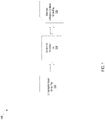
- FIG. 1 is a block diagram of an exemplary process 100 for obtaining a modified mask write file.
- a lithography mask write file (LMWF) 102 is provided.
- the LMWF 102 includes a set of instructions that may be used by a lithography tool (e.g., an electron beam lithography system) to pattern a surface during an exposure process.
- a lithography tool e.g., an electron beam lithography system
- the instructions from LMWF 102 may include instructions for directing and scanning a focused electron beam to define a geometric feature during a resist exposure process.
- the instructions may also define the feature dimensions of the geometric features to be produced.
- Feature dimensions include, e.g., radii, curves, lengths, widths, and/or aperture openings, among other feature dimensions.
- the instructions may also include dwell time instructions that specify the speed of the raster of an electron beam over a surface during the exposure process.
- the instructions specify how the geometric features defined by the electron beam are arranged along a two-dimensional plane.
- a LMWF 102 may include instructions for patterning of three-dimensional features.
- the LMWF 102 may provide instructions to a lithography system such that a wall of the mask is patterned at a particular angle.
- the LMWF 102 may include instructions for using low-kV electron beam lithography to pattern three-dimension features including angled openings in a mask.
- the fabrication of circuit elements may require the use of multiple LMWFs, where each LMWF provides instructions for a different mask to be used in a different fabrication step of a circuit fabrication process.
- the fabrication of a Josephson junction entails the deposition and patterning of two different resist layers, in which a different mask is applied to each resist layer.
- the features defined by the different masks may correspond to different aspects of the Josephson junction (e.g., bottom contact or a top contact).
- the LMWF 102 includes instructions for defining features to be formed on a photomask instead of instructions for directing an electron beam during e-beam lithography.
- the LMWF 102 may include instructions executable by computer aided design programs, such as AutoCAD®.
- the instructions of the LMWF may define the geometric dimensions of features to be formed on the photomask, as well as the arrangement of the features on the photomask.
- a uniformity function 104 may be applied to the lithography mask write file 102 to generate a modified lithography mask write file 106.
- a uniformity function 104 includes one or more functions that modify the lithography instructions of the LMWF 102.
- the modifications may include alterations to one or more feature defined by the LMWF 102.
- the modifications may include a change in the geometry and/or size of a feature defined by the LMWF 102.
- the modifications may include a change in dwell time instructions for an electron beam of the lithography tool.
- the uniformity function 104 may include a linear function component, a radial dependent component, a non-linear component, or a combination thereof that alters the features defined by the LMWF 102.
- a data processing apparatus receives a LMWF 102, and applies a uniformity function 104 to a LMWF 102 to generate a modified LMWF.
- a LMWF 102 may include instructions for an electron beam lithography tool for patterning a set of features (e.g., contact pads) in a grid layout across a resist mask on a substrate.
- a computer program on the data processing apparatus may then receive as inputs the LMWF 102 and the uniformity function 104, and apply the uniformity function 104 to the LMWF 102 such that the uniformity function 104 modifies one or more aspects of the features (e.g., size and/or location of the contact pads) to compensate for non-uniformities (e.g., film thickness variation) in the deposition process to be performed.
- the uniformity function 104 modifies one or more aspects of the features (e.g., size and/or location of the contact pads) to compensate for non-uniformities (e.g., film thickness variation) in the deposition process to be performed.
- Applying the uniformity function 104 to the LMWF 102 to create a modified LMWF 106 may include, but is not limited to, applying a function that changes a feature dimension of one or more features defined by the LMWF 102, applying a function that shifts a location of one or more features defined by the LMWF 102 relative to another feature or relative to a specified position within the mask, and/or applying a function that changes a dwell time of an electron beam defined by the LMWF 102.
- Feature dimensions that may be modified by the uniformity function 104 include, e.g., radii, curves, lengths, widths, and/or aperture openings, among other feature dimensions.
- a different uniformity function may be applied to each LMWF in a set of LMWFs for fabrication of circuit elements that requires the use of multiple masks.
- the feature changes produced by application of the uniformity function 104 to the LMWF 102 compensate for one or more non-uniformities in the deposition process. That is, structures that are fabricated using the modified LMWF 106 as a mask during the fabrication process may have features (e.g., geometric dimensions and/or location on a substrate surface) that are modified to compensate for variations resulting from deposition process (e.g., deposited film thickness variations).
- a LMWF 102 may define the shape and locations of portions of quantum computing circuit elements.
- the LMWF 102 may define the shape and location of multiple different Josephson junctions across a mask.
- the LMWF 102 also may specify that the shape of each quantum computing circuit element portion (e.g., each Josephson junction) is the same regardless of location within the mask.
- junction performance may vary depending on the thickness of the deposited contacts, and the thickness may be correlated with junction resistance, which, in turn, is proportional to a cross-sectional area of an oxide layer between the top and bottom contacts forming the junction.
- a spatial variation in the thickness of the deposited film used to form the contacts may result in the fabrication of multiple Josephson junctions one or more of which exhibit different junction resistances depending on the location of the junctions on the substrate.
- a uniformity function 104 may be applied to the LMWF 102 to produce a modified LMWF 106 that defines a modified shape and/or location of the quantum computing circuit element portions (e.g., the Josephson junction contacts) within the mask.
- the particular change that is applied to each quantum computing circuit element portion may be different depending on the location of the quantum computing circuit element portion within the mask.
- the changes applied to the quantum computing circuit element portion take into account the process variations (e.g., deposited film thickness variation) that may occur with fabrication in order to compensate for those variations (e.g., to provide Josephson junction contacts having uniform performance).
- process variations e.g., deposited film thickness variation
- the area of the contact along a plane orthogonal to the thickness direction (as defined by the lithography mask write file)
- Modifying the area of the contact along a plane orthogonal to the thickness direction preserves a total contact area. The increase in contact area may counter the decrease in film thickness.
- the modified LMWF 106 then may be used to form a mask that defines the Josephson junction contact areas.
- the uniformity function 104 applied to a LMWF 102 may compensate for non-uniformities of two or more depositions in a multi-deposition fabrication process.
- a first deposition step may have a unique non-uniform process variation relative to other deposition steps within the fabrication process. Differences in non-uniformity of deposition between deposition steps may be due to a variety of factors including, a difference in substrate rotation in the different steps, a difference in the angle of orientation of the substrate surface relative to a deposition beam source, and a difference in shadow effects by the resist mask between deposition steps.
- a shadow effect may occur when a part of a substrate area is shadowed or obscured by a resist mask such that a deposition beam is limited or blocked from depositing material on the substrate area.
- Another shadow effect may occur when a surface of deposition of a substrate is angled with respect to the deposition beam such that the deposition beam is shadowed or obscured from depositing material on the substrate area.
- one or more deposition steps may affect subsequent depositions. For example, for a first deposition for fabricating a Josephson junction, some amount of material may be deposited on at least a sidewall of a resist mask. For a second, subsequent deposition through the same mask, a deposition beam may be further shadowed by the material previously deposited on one or more sidewalls of the resist mask in the first deposition. The additional shadowing due to the sidewall deposition may limit the amount of deposition possible through the resist mask. This in turn may affect a width of a line that is deposited in the second, subsequent deposition. Changing the width of the deposited line may change the cross-sectional area of the junction and may in turn affect the resistance of the Josephson junction.
- a uniformity function 104 may reduce the non-uniformity of deposition resulting from the sidewall deposition by modifying a LMWF 102 to generate a modified LMWF (e.g., MLMWF 106).
- the LMWF 102 defines a lithography pattern that is copied multiple times across a mask using a stitching process.
- a different uniformity function 104 may be generated and applied to different regions of the mask defined by the LMWF 102.
- the particular uniformity function 104 that will be used at each different region may depend on the expected process variation to occur that region. For example, a uniformity function applied to a feature pattern in a region adjacent to a mask edge may differ from a uniformity function applied to the same feature pattern that is located in a region adjacent to a central portion of the mask.
- a uniformity function 104 for modifying a LMWF 102 may be generated using one or more different methods.
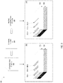
- FIGS. 2A , 2B are block diagrams illustrating exemplary processes 200 and 250 for generating uniformity functions from deposition data and from one or more geometric arguments, respectively.
- a uniformity function 104 in exemplary process 200 is generated empirically by a calibration process 202 having a fabrication and a characterization step 204.
- the calibration process 202 includes fabrication (206) of at least one test structure on a substrate and characterization (208) of the at least one test structure.
- An example of a test structure includes a thin film deposited across at least a portion of the substrate.
- a test structure may also be a Josephson junction.
- Other test structures are also possible. Test structures may be deposited directly onto a substrate or may be deposited through a mask. In some implementations, test structures may be deposited onto a substrate and undergo post-processing steps including lithography and/or etching.
- the fabrication (206) of the at least one test structure may be performed according to one or more specified depositions parameters ⁇ Dp ⁇ 210.
- deposition parameters include, but are not limited to, deposition tool parameters 210-1, deposition conditions 210-2, and geometry of deposited structures 210-3, the details of which will be described further below.
- the at least one fabricated test structure then may be characterized (208) to extract deposition data 212.
- the deposition data 212 may include, in some implementations, non-uniformity deposition results (e.g., non-uniform resistance or film thickness across a substrate).
- Characterization of at least one fabricated test structure may include, e.g., measuring, directly or indirectly, information about the geometric dimensions of the test structure. For example, a direct characterization of a test structure (e.g., a wire) may use atomic force microscopy (AFM) to measure the geometric dimensions (e.g., width, length, radius, thickness) of the features of the test structure.
- AFM atomic force microscopy
- An example of an indirect characterization may rely on a four-point probe measurement of the test structure (e.g., a thin film deposited on a substrate of known resistivity).
- the sheet resistance R s may be determined from the four-point probe based on a relationship between the measured voltage V and measured current I between the probes.
- Another example of an indirect characterization of Josephson junctions may rely on room-temperature DC probing for measurement of resistances across a wafer. The room-temperature DC probing yields an (x,y)-dependent resistance map across the wafer, which can then be used to extract information about the cross-sectional area of the junction.
- a set of deposition data ⁇ D N ⁇ 212 is collected from the characterization of the test structures 208, including information pertaining to non-uniformity in the deposition of the test structures.
- the function 214 may characterize certain deposition data (e.g., film thickness) as varying linearly, radially or non-linearly across a substrate surface for different angles at which the substrate surface is oriented with respect to a deposition source.
- a component is a non-linear function such as a cubic function or a quadratic function.
- the source direction is a unity vector pointing along the z axis (e.g., (0,0,1)).
- the empirical function 214 may be used to generate at least one uniformity function 104.
- a data processing apparatus e.g., a computer
- the data processing apparatus may then take as inputs the empirical function 214 and use the established relationship between resistance and cross-sectional area described herein, and generate a uniformity function 104.
- the deposition data 212 for a calibration process 202 may yield a different empirical function, generating a different uniformity function 104.
- the uniformity function 104 can then be applied to a LMWF 102 to create a modified LMWF 106.
- a series of geometric arguments can be formulated to compensate for non-uniformities in deposition.
- the one or more geometric arguments may be part of a geometric model or geometric simulation.
- a geometric argument 216 relates one or more deposition parameters 210 to one or more effects on deposition.
- a geometric argument may specify the effect on deposition thickness across a way as a function of an angle of deposition (e.g., the angle of the surface of a substrate relative to the angle of a deposition beam), such that the non-uniformity is a function of the angle of deposition.
- the deposition tool parameters 210-1 vary between deposition tools, and may be adjustable or static depending on the tool.
- Deposition tools include electron beam evaporation systems, physical vapor deposition systems, atomic layer deposition systems, chemical vapor deposition systems, molecular beam epitaxy systems, and the like.
- Deposition tool parameters include source-to-substrate distances, deposition rates, range of deposition angles, and deposition beam profile. For example, a larger source-to-substrate distance will ensure a higher degree of uniformity of deposition across a substrate due to a reduced angular dependence of the deposition. However, fewer deposition tools have this feature due to the required overall height of the tool for a large source-to-substrate distance.
- Geometry of deposited structures 210-3 include, parallel strips, crossed wires, coplanar waveguides, concentric circles, concentric squares, angled strips, tapered strips, circles, squares, and the like.
- the geometry of a set of deposited structures 210-3 additionally affects non-uniformity of the deposited structures.
- a first deposition on a substrate may affect subsequent depositions on the same substrate by creating additional shadowing affects. For example, a geometry including a two-step deposition process through a resist mask onto a substrate for depositing a pair of crossed wires, where each wire is deposited in a separate deposition step.
- a first deposition for a first wire may have the additional effect of depositing excess material on top of a resist mask.
- a geometric function F G ( ⁇ D P ⁇ ) 218 may be generated by a data processing apparatus.
- the geometric function 218 may include one or more geometric arguments 216 that establishes a geometric relationship between a given set of deposition parameters ⁇ D P ⁇ 210 and a set of simulated non-uniformity effects.
- the geometric function 218 may include information including film thickness variation, electrode width variation, sidewall variation, and resist aperture variation.
- the geometric function 218 further incorporates geometric and deposition considerations of the above mentioned deposition parameters. For each set of deposition data 210, the geometric function F G ( ⁇ D P ⁇ ) 218 generates at least one uniformity function 104 which can be applied to a LMWF 102 to create a modified LMWF 106.
- LMWF 102 contains instructions for the lithography tool (e.g., electron beam lithography tool) regarding the dimensions and layout with respect to a substrate of each feature 308-1, 308-2, and 308-3 such that the electron beam may selectively cure the areas where the features occur or the areas where the features do not occur, depending on the type of resist used.
- the instructions of the LMWF also include a dwell time or speed at which the electron beam rasters the surface, curing through the thickness of the resist layer.
- the mask features 308-1, 308-2, and 308-3 are all rectangular features of equal dimensions.
- the area of overlap between the top and bottom contacts may depend on the height of the bottom contact, which is dependent on the thickness of deposition.
- a rectangular wire bottom contact has a length, width, and height, wherein the height of the bottom contact is defined, in part, by the thickness of the film deposited at the location of the junction.
- the rectangular wire may have a top surface and one or more sidewalls.
- the one or more sidewalls may be defined as having a surface perpendicular to the surface of the substrate, and where the height of the sidewalls is defined by the thickness of the deposited film.
- An oxide layer promoted on the exposed surfaces of the rectangular wire may then include oxide formation on all exposed surfaces of the rectangular wire, including one or more sidewalls of the wire.
- a second, top contact e.g., a rectangular wire
- deposited on top of the oxide layer may then overlap the bottom contact (and oxide layer) over multiple exposed surfaces (e.g., a top surface and one or more sidewalls).
- Different forms of modification to a set of instructions in a modified LMWF may be implemented to compensate for various non-uniformities.
- Josephson junctions deposited across a substrate may have non-uniform junction cross-sectional areas, resulting in non-uniform junction resistances.
- FIG. 3 depicts a uniformity function 104 that includes a linear function for compensating for a linear non-uniformity of deposition, there can be multiple other forms of modifications applied by a uniformity function 104 as mentioned above.
- a uniformity function 104 is obtained (404) from an empirical function 214, a geometric function 218, or a combination thereof.
- the uniformity function 104 is obtained (404) by a data processing apparatus.
- the uniformity function 104 compensates for the non-uniformity deposition effects resulting from the deposition parameters 210 used in the fabrication process by modifying a LMWF 102 to generate a modified LMWF 106.
- a short source-to-substrate distance in a deposition tool e.g., an electron beam evaporation system
- an offset in uniformity from the center of the substrate may result from beam location, substrate tilt, substrate offset from center, or the like.
- a modified LMWF 106 is obtained (408) from the application of the uniformity function 104 to the LMWF 102.
- a data processing apparatus may obtain the modified LMWF 106 from the application of the uniformity function 104 to the LMWF 102.
- the modified LMWF 106 may have some or none of the same instructions from the original LMWF. For example, lithography is performed using the modified LMWF 106 to define a pattern that will be used for shadow evaporation of a superconducting material to form a set of Josephson junctions on the sample substrate.
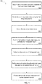
- FIG. 5 is a flow chart of an example process for fabricating a set of Josephson junctions with improved junction resistance uniformity on a sample substrate.
- One or more resist layers are deposited onto a substrate to form one or more resist masks (502). Deposition of resist layers may be through spin coating.
- Various compositions of resist may be used including poly(methyl methacrylate) (PMMA).
- Resists may be positive or negative resists, where the positive resist is exposed in regions that will be removed from the resist mask and negative resist is exposed in all the regions that will be part of the resist mask.
- the sample substrate is returned to the deposition tool, and a second deposition through the resist mask layers onto the substrate is performed (512).
- the second deposition is performed at a second substrate surface deposition angle (relative to the deposition beam axis).
- the second deposition angle may be orthogonal to the first deposition angle.
- the substrate is rotated to a second position in the deposition chamber different from the first position.
- the sample is processed to lift-off the resist mask layers as well as any excess deposition (514).
- one or more solvents e.g., acetone
- other chemical compounds e.g., resist strippers
- ultrasonic immersion e.g., heated bath, or a combination thereof may be used.
- An example of a superconductor material that can be used in the formation of quantum circuit elements is aluminum.
- Aluminum may be used in combination with a dielectric to establish Josephson junctions, which are a common component of quantum circuit elements.
- quantum circuit elements that may be formed with aluminum include circuit elements such as superconducting co-planar waveguides, quantum LC oscillators, qubits (e.g., flux qubits or charge qubits), superconducting quantum interference devices (SQUIDs) (e.g., RF-SQUID or DC-SQUID), inductors, capacitors, transmission lines, ground planes, among others.
- qubits e.g., flux qubits or charge qubits
- SQUIDs superconducting quantum interference devices
- inductors e.g., RF-SQUID or DC-SQUID
- capacitors e.g., transmission lines, ground planes, among others.
- quantum memories are devices that can store quantum data for a long time with high fidelity and efficiency, e.g., light-matter interfaces where light is used for transmission and matter for storing and preserving the quantum features of quantum data such as superposition or quantum coherence.
- a computer can be embedded in another device, e.g., a mobile telephone, a personal digital assistant (PDA), a mobile audio or video player, a game console, a Global Positioning System (GPS) receiver, or a portable storage device (e.g., a universal serial bus (USB) flash drive), to name just a few.
- Devices suitable for storing computer program instructions and data include all forms of non-volatile memory, media and memory devices, including by way of example semiconductor memory devices, e.g., EPROM, EEPROM, and flash memory devices; magnetic disks, e.g., internal hard disks or removable disks; magneto-optical disks; and CD-ROM and DVD-ROM disks.
- the processor and the memory can be supplemented by, or incorporated in, special purpose logic circuitry.
- Embodiments of the subject matter described in this specification can be implemented in a computing system that includes a back-end component, e.g., as a data server, or that includes a middleware component, e.g., an application server, or that includes a front-end component, e.g., a user computer having a graphical user interface or a Web browser through which a user can interact with an implementation of the subject matter described in this specification, or any combination of one or more such back-end, middleware, or front-end components.
- the components of the system can be interconnected by any form or medium of digital data communication, e.g., a communication network.
Landscapes
- Chemical & Material Sciences (AREA)
- Physics & Mathematics (AREA)
- Engineering & Computer Science (AREA)
- General Physics & Mathematics (AREA)
- Chemical Kinetics & Catalysis (AREA)
- Materials Engineering (AREA)
- Mechanical Engineering (AREA)
- Metallurgy (AREA)
- Organic Chemistry (AREA)
- Nanotechnology (AREA)
- Crystallography & Structural Chemistry (AREA)
- Manufacturing & Machinery (AREA)
- General Chemical & Material Sciences (AREA)
- Theoretical Computer Science (AREA)
- Mathematical Physics (AREA)
- Condensed Matter Physics & Semiconductors (AREA)
- Plasma & Fusion (AREA)
- Exposure And Positioning Against Photoresist Photosensitive Materials (AREA)
- Superconductor Devices And Manufacturing Methods Thereof (AREA)
- Electron Beam Exposure (AREA)
- Preparing Plates And Mask In Photomechanical Process (AREA)
Applications Claiming Priority (3)
| Application Number | Priority Date | Filing Date | Title |
|---|---|---|---|
| US201662440566P | 2016-12-30 | 2016-12-30 | |
| PCT/US2017/064182 WO2018125513A1 (en) | 2016-12-30 | 2017-12-01 | Compensating deposition non-uniformities in circuit elements |
| EP17825661.6A EP3475760B1 (de) | 2016-12-30 | 2017-12-01 | Kompensieren von ablagerungsungleichförmigkeiten in schaltungselementen |
Related Parent Applications (2)
| Application Number | Title | Priority Date | Filing Date |
|---|---|---|---|
| EP17825661.6A Division-Into EP3475760B1 (de) | 2016-12-30 | 2017-12-01 | Kompensieren von ablagerungsungleichförmigkeiten in schaltungselementen |
| EP17825661.6A Division EP3475760B1 (de) | 2016-12-30 | 2017-12-01 | Kompensieren von ablagerungsungleichförmigkeiten in schaltungselementen |
Publications (2)
| Publication Number | Publication Date |
|---|---|
| EP3660179A1 true EP3660179A1 (de) | 2020-06-03 |
| EP3660179B1 EP3660179B1 (de) | 2023-03-29 |
Family
ID=60935953
Family Applications (2)
| Application Number | Title | Priority Date | Filing Date |
|---|---|---|---|
| EP19212172.1A Active EP3660179B1 (de) | 2016-12-30 | 2017-12-01 | Kompensieren von ablagerungsungleichförmigkeiten in schaltungselementen |
| EP17825661.6A Active EP3475760B1 (de) | 2016-12-30 | 2017-12-01 | Kompensieren von ablagerungsungleichförmigkeiten in schaltungselementen |
Family Applications After (1)
| Application Number | Title | Priority Date | Filing Date |
|---|---|---|---|
| EP17825661.6A Active EP3475760B1 (de) | 2016-12-30 | 2017-12-01 | Kompensieren von ablagerungsungleichförmigkeiten in schaltungselementen |
Country Status (6)
| Country | Link |
|---|---|
| US (3) | US10990017B2 (de) |
| EP (2) | EP3660179B1 (de) |
| JP (1) | JP6706391B2 (de) |
| CN (2) | CN109844637B (de) |
| CA (1) | CA3034528C (de) |
| WO (1) | WO2018125513A1 (de) |
Families Citing this family (10)
| Publication number | Priority date | Publication date | Assignee | Title |
|---|---|---|---|---|
| EP3660179B1 (de) | 2016-12-30 | 2023-03-29 | Google LLC | Kompensieren von ablagerungsungleichförmigkeiten in schaltungselementen |
| US10608157B2 (en) | 2017-05-18 | 2020-03-31 | International Business Machines Corporation | Qubit network non-volatile identification |
| US10826713B2 (en) * | 2017-05-18 | 2020-11-03 | International Business Machines Corporation | Qubit network secure identification |
| US10503077B2 (en) * | 2017-11-07 | 2019-12-10 | International Business Machines Corporation | Shadow mask area correction for tunnel junctions |
| US11024792B2 (en) | 2019-01-25 | 2021-06-01 | Microsoft Technology Licensing, Llc | Fabrication methods |
| WO2021112856A1 (en) | 2019-12-05 | 2021-06-10 | Microsoft Technology Licensing, Llc | Method of fabricating a hollow wall for controlling directional deposition of material |
| AU2022289736A1 (en) | 2021-06-11 | 2024-02-01 | Caleb JORDAN | System and method of flux bias for superconducting quantum circuits |
| WO2023203679A1 (ja) * | 2022-04-20 | 2023-10-26 | 富士通株式会社 | ジョセフソン接合素子の製造方法および量子ビットの製造方法 |
| CN117979812A (zh) * | 2022-10-21 | 2024-05-03 | 腾讯科技(深圳)有限公司 | 芯片制备方法、系统及芯片 |
| FR3150039A1 (fr) * | 2023-06-16 | 2024-12-20 | Commissariat A L'energie Atomique Et Aux Energies Alternatives | Procede de mesure de la resistance et de la capacitance de films minces en cours de depot domaine technique et état de la technique antérieure |
Citations (3)
| Publication number | Priority date | Publication date | Assignee | Title |
|---|---|---|---|---|
| US20040058255A1 (en) * | 2002-09-24 | 2004-03-25 | Scott Jessen | Substrate topography compensation at mask design: 3D OPC topography anchored |
| US20090235224A1 (en) * | 2008-03-13 | 2009-09-17 | Hynix Semiconductor Inc. | Method for Processing Optical Proximity Correction |
| US20110151190A1 (en) * | 2007-05-08 | 2011-06-23 | Jae-Hyun Chung | Shadow edge lithography for nanoscale patterning and manufacturing |
Family Cites Families (16)
| Publication number | Priority date | Publication date | Assignee | Title |
|---|---|---|---|---|
| US6883158B1 (en) * | 1999-05-20 | 2005-04-19 | Micronic Laser Systems Ab | Method for error reduction in lithography |
| JP2001244181A (ja) | 2000-02-29 | 2001-09-07 | Nippon Telegr & Teleph Corp <Ntt> | 電子線描画データ加工方法および描画データ加工プログラムを記録した記録媒体、ならびに電子線描画装置 |
| US6402905B1 (en) | 2001-03-16 | 2002-06-11 | 4 Wave, Inc | System and method for controlling deposition thickness using a mask with a shadow that varies along a radius of a substrate |
| JP2005217047A (ja) * | 2004-01-28 | 2005-08-11 | Sony Corp | マスク、露光方法および半導体装置の製造方法 |
| JP4351928B2 (ja) * | 2004-02-23 | 2009-10-28 | 株式会社東芝 | マスクデータの補正方法、フォトマスクの製造方法及びマスクデータの補正プログラム |
| EP1619556A1 (de) * | 2004-07-20 | 2006-01-25 | Interuniversitair Micro-Elektronica Centrum | Verfahren und Masken zur Reduzierung der Auswirkung von Streulicht in der optischen Lithographie |
| JP4747112B2 (ja) | 2007-02-01 | 2011-08-17 | 株式会社ニューフレアテクノロジー | パターン形成方法及び荷電粒子ビーム描画装置 |
| US8181128B2 (en) * | 2008-10-13 | 2012-05-15 | Synopsys, Inc. | Method and apparatus for determining a photolithography process model which models the influence of topography variations |
| KR20130069037A (ko) * | 2011-12-16 | 2013-06-26 | 삼성디스플레이 주식회사 | 유기층 증착 장치, 이를 이용한 유기 발광 표시 장치의 제조 방법 및 유기 발광 표시 장치 |
| US8941187B2 (en) * | 2012-01-13 | 2015-01-27 | Globalfoundries Inc. | Strain engineering in three-dimensional transistors based on strained isolation material |
| US8793626B2 (en) * | 2012-03-23 | 2014-07-29 | Texas Instruments Incorporated | Computational lithography with feature upsizing |
| US8954919B1 (en) * | 2013-11-01 | 2015-02-10 | United Microelectronics Corp. | Calculation method for generating layout pattern in photomask |
| WO2017202665A1 (en) | 2016-05-25 | 2017-11-30 | Asml Netherlands B.V. | Focus and overlay improvement by modifying a patterning device |
| US10197908B2 (en) * | 2016-06-21 | 2019-02-05 | Lam Research Corporation | Photoresist design layout pattern proximity correction through fast edge placement error prediction via a physics-based etch profile modeling framework |
| US10254641B2 (en) * | 2016-12-01 | 2019-04-09 | Lam Research Corporation | Layout pattern proximity correction through fast edge placement error prediction |
| EP3660179B1 (de) | 2016-12-30 | 2023-03-29 | Google LLC | Kompensieren von ablagerungsungleichförmigkeiten in schaltungselementen |
-
2017
- 2017-12-01 EP EP19212172.1A patent/EP3660179B1/de active Active
- 2017-12-01 US US16/325,319 patent/US10990017B2/en active Active
- 2017-12-01 EP EP17825661.6A patent/EP3475760B1/de active Active
- 2017-12-01 JP JP2019510631A patent/JP6706391B2/ja active Active
- 2017-12-01 CN CN201780051576.2A patent/CN109844637B/zh active Active
- 2017-12-01 WO PCT/US2017/064182 patent/WO2018125513A1/en not_active Ceased
- 2017-12-01 CN CN202211009872.5A patent/CN115480457B/zh active Active
- 2017-12-01 CA CA3034528A patent/CA3034528C/en active Active
-
2021
- 2021-03-22 US US17/208,391 patent/US11378890B2/en active Active
-
2022
- 2022-07-01 US US17/856,564 patent/US11662664B2/en active Active
Patent Citations (3)
| Publication number | Priority date | Publication date | Assignee | Title |
|---|---|---|---|---|
| US20040058255A1 (en) * | 2002-09-24 | 2004-03-25 | Scott Jessen | Substrate topography compensation at mask design: 3D OPC topography anchored |
| US20110151190A1 (en) * | 2007-05-08 | 2011-06-23 | Jae-Hyun Chung | Shadow edge lithography for nanoscale patterning and manufacturing |
| US20090235224A1 (en) * | 2008-03-13 | 2009-09-17 | Hynix Semiconductor Inc. | Method for Processing Optical Proximity Correction |
Also Published As
| Publication number | Publication date |
|---|---|
| EP3475760B1 (de) | 2020-02-12 |
| CN109844637A (zh) | 2019-06-04 |
| US20230119165A1 (en) | 2023-04-20 |
| US20210208509A1 (en) | 2021-07-08 |
| JP2020502551A (ja) | 2020-01-23 |
| WO2018125513A1 (en) | 2018-07-05 |
| US20190204753A1 (en) | 2019-07-04 |
| EP3475760A1 (de) | 2019-05-01 |
| CA3034528C (en) | 2022-08-16 |
| JP6706391B2 (ja) | 2020-06-03 |
| CN115480457A (zh) | 2022-12-16 |
| US10990017B2 (en) | 2021-04-27 |
| EP3660179B1 (de) | 2023-03-29 |
| US11378890B2 (en) | 2022-07-05 |
| CA3034528A1 (en) | 2018-07-05 |
| US11662664B2 (en) | 2023-05-30 |
| CN109844637B (zh) | 2022-09-09 |
| CN115480457B (zh) | 2024-03-12 |
Similar Documents
| Publication | Publication Date | Title |
|---|---|---|
| US11662664B2 (en) | Compensating deposition non-uniformities in circuit elements | |
| US11903329B2 (en) | Reducing junction resistance variation in two-step deposition processes | |
| TW202341018A (zh) | 用於模擬量子計算的方法及系統 | |
| US10622267B2 (en) | Facilitation of spin-coat planarization over feature topography during substrate fabrication | |
| CN104730858B (zh) | 采用反馈控制改善晶圆图案化的均匀性 | |
| WO2024050152A2 (en) | Modifiable quantum error correction code for logical qubits | |
| Davaji et al. | Deep learning for predicting CD-SEMS of NEMS devices | |
| Constantoudis et al. | Line-edge-roughness transfer during plasma etching: modeling approaches and comparison with experimental results | |
| US20250386741A1 (en) | Compensating spatially-dependent circuit fabrication non-uniformities | |
| CN103855075B (zh) | 刻蚀条件的采集方法 | |
| Kojima et al. | Study of device mass production capability of the character projection based electron beam direct writing process technology toward 14 nm node and beyond | |
| Reznik et al. | The near-field microwave technique for deep profiling of free carrier concentration in semiconductors | |
| Andreeva et al. | Reservoir Network Based on Single Impurity Atoms in Silicon | |
| Kris et al. | Beyond 3 sigma: roughness metrology evolution at the last 20 years (in memory of Ben Bunday) | |
| BR102024012771A2 (pt) | Dispositivo de junção josephson tipo ferradura e o método de fabricação do dispositivo | |
| CN120525074A (zh) | 一种硅基单原子量子计算芯片及其制备方法 | |
| CN118489069A (zh) | 用于模拟量子计算的方法及系统 | |
| Johnson | Optimization of superconducting flux qubit readout using near-quantum-limited amplifiers | |
| Tsarik et al. | Formation of nanosized elements by ion beam lithography for multiple fin field effect transistor prototyping | |
| Samukawa | Prediction of abnormal etching profiles in high-aspect-ratio via/hole etching using on-wafer monitoring system | |
| Ruvich | Fabrication of microwave resonators in titanium nitride using photolithography |
Legal Events
| Date | Code | Title | Description |
|---|---|---|---|
| PUAI | Public reference made under article 153(3) epc to a published international application that has entered the european phase |
Free format text: ORIGINAL CODE: 0009012 |
|
| STAA | Information on the status of an ep patent application or granted ep patent |
Free format text: STATUS: THE APPLICATION HAS BEEN PUBLISHED |
|
| AC | Divisional application: reference to earlier application |
Ref document number: 3475760 Country of ref document: EP Kind code of ref document: P |
|
| AK | Designated contracting states |
Kind code of ref document: A1 Designated state(s): AL AT BE BG CH CY CZ DE DK EE ES FI FR GB GR HR HU IE IS IT LI LT LU LV MC MK MT NL NO PL PT RO RS SE SI SK SM TR |
|
| AX | Request for extension of the european patent |
Extension state: BA ME |
|
| RAP1 | Party data changed (applicant data changed or rights of an application transferred) |
Owner name: GOOGLE LLC |
|
| STAA | Information on the status of an ep patent application or granted ep patent |
Free format text: STATUS: REQUEST FOR EXAMINATION WAS MADE |
|
| 17P | Request for examination filed |
Effective date: 20201116 |
|
| RBV | Designated contracting states (corrected) |
Designated state(s): AL AT BE BG CH CY CZ DE DK EE ES FI FR GB GR HR HU IE IS IT LI LT LU LV MC MK MT NL NO PL PT RO RS SE SI SK SM TR |
|
| REG | Reference to a national code |
Ref country code: DE Ref legal event code: R079 Ref document number: 602017067359 Country of ref document: DE Free format text: PREVIOUS MAIN CLASS: C23C0014040000 Ipc: C23C0014140000 |
|
| RIC1 | Information provided on ipc code assigned before grant |
Ipc: B82Y 40/00 20110101ALI20220826BHEP Ipc: B82Y 10/00 20110101ALI20220826BHEP Ipc: G03F 1/78 20120101ALI20220826BHEP Ipc: G03F 1/76 20120101ALI20220826BHEP Ipc: G03F 7/20 20060101ALI20220826BHEP Ipc: H01L 39/24 20060101ALI20220826BHEP Ipc: C23C 14/22 20060101ALI20220826BHEP Ipc: C23C 14/04 20060101ALI20220826BHEP Ipc: C23C 14/14 20060101AFI20220826BHEP |
|
| GRAP | Despatch of communication of intention to grant a patent |
Free format text: ORIGINAL CODE: EPIDOSNIGR1 |
|
| STAA | Information on the status of an ep patent application or granted ep patent |
Free format text: STATUS: GRANT OF PATENT IS INTENDED |
|
| INTG | Intention to grant announced |
Effective date: 20221010 |
|
| GRAS | Grant fee paid |
Free format text: ORIGINAL CODE: EPIDOSNIGR3 |
|
| GRAA | (expected) grant |
Free format text: ORIGINAL CODE: 0009210 |
|
| STAA | Information on the status of an ep patent application or granted ep patent |
Free format text: STATUS: THE PATENT HAS BEEN GRANTED |
|
| AC | Divisional application: reference to earlier application |
Ref document number: 3475760 Country of ref document: EP Kind code of ref document: P |
|
| AK | Designated contracting states |
Kind code of ref document: B1 Designated state(s): AL AT BE BG CH CY CZ DE DK EE ES FI FR GB GR HR HU IE IS IT LI LT LU LV MC MK MT NL NO PL PT RO RS SE SI SK SM TR |
|
| REG | Reference to a national code |
Ref country code: CH Ref legal event code: EP |
|
| REG | Reference to a national code |
Ref country code: DE Ref legal event code: R096 Ref document number: 602017067359 Country of ref document: DE |
|
| REG | Reference to a national code |
Ref country code: AT Ref legal event code: REF Ref document number: 1556708 Country of ref document: AT Kind code of ref document: T Effective date: 20230415 |
|
| REG | Reference to a national code |
Ref country code: NL Ref legal event code: FP Ref country code: IE Ref legal event code: FG4D |
|
| P01 | Opt-out of the competence of the unified patent court (upc) registered |
Effective date: 20230518 |
|
| REG | Reference to a national code |
Ref country code: LT Ref legal event code: MG9D |
|
| PG25 | Lapsed in a contracting state [announced via postgrant information from national office to epo] |
Ref country code: RS Free format text: LAPSE BECAUSE OF FAILURE TO SUBMIT A TRANSLATION OF THE DESCRIPTION OR TO PAY THE FEE WITHIN THE PRESCRIBED TIME-LIMIT Effective date: 20230329 Ref country code: NO Free format text: LAPSE BECAUSE OF FAILURE TO SUBMIT A TRANSLATION OF THE DESCRIPTION OR TO PAY THE FEE WITHIN THE PRESCRIBED TIME-LIMIT Effective date: 20230629 Ref country code: LV Free format text: LAPSE BECAUSE OF FAILURE TO SUBMIT A TRANSLATION OF THE DESCRIPTION OR TO PAY THE FEE WITHIN THE PRESCRIBED TIME-LIMIT Effective date: 20230329 Ref country code: LT Free format text: LAPSE BECAUSE OF FAILURE TO SUBMIT A TRANSLATION OF THE DESCRIPTION OR TO PAY THE FEE WITHIN THE PRESCRIBED TIME-LIMIT Effective date: 20230329 Ref country code: HR Free format text: LAPSE BECAUSE OF FAILURE TO SUBMIT A TRANSLATION OF THE DESCRIPTION OR TO PAY THE FEE WITHIN THE PRESCRIBED TIME-LIMIT Effective date: 20230329 |
|
| REG | Reference to a national code |
Ref country code: AT Ref legal event code: MK05 Ref document number: 1556708 Country of ref document: AT Kind code of ref document: T Effective date: 20230329 |
|
| PG25 | Lapsed in a contracting state [announced via postgrant information from national office to epo] |
Ref country code: SE Free format text: LAPSE BECAUSE OF FAILURE TO SUBMIT A TRANSLATION OF THE DESCRIPTION OR TO PAY THE FEE WITHIN THE PRESCRIBED TIME-LIMIT Effective date: 20230329 Ref country code: GR Free format text: LAPSE BECAUSE OF FAILURE TO SUBMIT A TRANSLATION OF THE DESCRIPTION OR TO PAY THE FEE WITHIN THE PRESCRIBED TIME-LIMIT Effective date: 20230630 Ref country code: FI Free format text: LAPSE BECAUSE OF FAILURE TO SUBMIT A TRANSLATION OF THE DESCRIPTION OR TO PAY THE FEE WITHIN THE PRESCRIBED TIME-LIMIT Effective date: 20230329 |
|
| PG25 | Lapsed in a contracting state [announced via postgrant information from national office to epo] |
Ref country code: SM Free format text: LAPSE BECAUSE OF FAILURE TO SUBMIT A TRANSLATION OF THE DESCRIPTION OR TO PAY THE FEE WITHIN THE PRESCRIBED TIME-LIMIT Effective date: 20230329 Ref country code: RO Free format text: LAPSE BECAUSE OF FAILURE TO SUBMIT A TRANSLATION OF THE DESCRIPTION OR TO PAY THE FEE WITHIN THE PRESCRIBED TIME-LIMIT Effective date: 20230329 Ref country code: PT Free format text: LAPSE BECAUSE OF FAILURE TO SUBMIT A TRANSLATION OF THE DESCRIPTION OR TO PAY THE FEE WITHIN THE PRESCRIBED TIME-LIMIT Effective date: 20230731 Ref country code: ES Free format text: LAPSE BECAUSE OF FAILURE TO SUBMIT A TRANSLATION OF THE DESCRIPTION OR TO PAY THE FEE WITHIN THE PRESCRIBED TIME-LIMIT Effective date: 20230329 Ref country code: EE Free format text: LAPSE BECAUSE OF FAILURE TO SUBMIT A TRANSLATION OF THE DESCRIPTION OR TO PAY THE FEE WITHIN THE PRESCRIBED TIME-LIMIT Effective date: 20230329 Ref country code: AT Free format text: LAPSE BECAUSE OF FAILURE TO SUBMIT A TRANSLATION OF THE DESCRIPTION OR TO PAY THE FEE WITHIN THE PRESCRIBED TIME-LIMIT Effective date: 20230329 |
|
| PG25 | Lapsed in a contracting state [announced via postgrant information from national office to epo] |
Ref country code: SK Free format text: LAPSE BECAUSE OF FAILURE TO SUBMIT A TRANSLATION OF THE DESCRIPTION OR TO PAY THE FEE WITHIN THE PRESCRIBED TIME-LIMIT Effective date: 20230329 Ref country code: PL Free format text: LAPSE BECAUSE OF FAILURE TO SUBMIT A TRANSLATION OF THE DESCRIPTION OR TO PAY THE FEE WITHIN THE PRESCRIBED TIME-LIMIT Effective date: 20230329 Ref country code: IS Free format text: LAPSE BECAUSE OF FAILURE TO SUBMIT A TRANSLATION OF THE DESCRIPTION OR TO PAY THE FEE WITHIN THE PRESCRIBED TIME-LIMIT Effective date: 20230729 |
|
| REG | Reference to a national code |
Ref country code: DE Ref legal event code: R097 Ref document number: 602017067359 Country of ref document: DE |
|
| PG25 | Lapsed in a contracting state [announced via postgrant information from national office to epo] |
Ref country code: DK Free format text: LAPSE BECAUSE OF FAILURE TO SUBMIT A TRANSLATION OF THE DESCRIPTION OR TO PAY THE FEE WITHIN THE PRESCRIBED TIME-LIMIT Effective date: 20230329 Ref country code: CZ Free format text: LAPSE BECAUSE OF FAILURE TO SUBMIT A TRANSLATION OF THE DESCRIPTION OR TO PAY THE FEE WITHIN THE PRESCRIBED TIME-LIMIT Effective date: 20230329 |
|
| PLBE | No opposition filed within time limit |
Free format text: ORIGINAL CODE: 0009261 |
|
| STAA | Information on the status of an ep patent application or granted ep patent |
Free format text: STATUS: NO OPPOSITION FILED WITHIN TIME LIMIT |
|
| 26N | No opposition filed |
Effective date: 20240103 |
|
| PG25 | Lapsed in a contracting state [announced via postgrant information from national office to epo] |
Ref country code: SI Free format text: LAPSE BECAUSE OF FAILURE TO SUBMIT A TRANSLATION OF THE DESCRIPTION OR TO PAY THE FEE WITHIN THE PRESCRIBED TIME-LIMIT Effective date: 20230329 |
|
| PG25 | Lapsed in a contracting state [announced via postgrant information from national office to epo] |
Ref country code: SI Free format text: LAPSE BECAUSE OF FAILURE TO SUBMIT A TRANSLATION OF THE DESCRIPTION OR TO PAY THE FEE WITHIN THE PRESCRIBED TIME-LIMIT Effective date: 20230329 Ref country code: IT Free format text: LAPSE BECAUSE OF FAILURE TO SUBMIT A TRANSLATION OF THE DESCRIPTION OR TO PAY THE FEE WITHIN THE PRESCRIBED TIME-LIMIT Effective date: 20230329 |
|
| REG | Reference to a national code |
Ref country code: CH Ref legal event code: PL |
|
| PG25 | Lapsed in a contracting state [announced via postgrant information from national office to epo] |
Ref country code: LU Free format text: LAPSE BECAUSE OF NON-PAYMENT OF DUE FEES Effective date: 20231201 |
|
| PG25 | Lapsed in a contracting state [announced via postgrant information from national office to epo] |
Ref country code: MC Free format text: LAPSE BECAUSE OF FAILURE TO SUBMIT A TRANSLATION OF THE DESCRIPTION OR TO PAY THE FEE WITHIN THE PRESCRIBED TIME-LIMIT Effective date: 20230329 |
|
| REG | Reference to a national code |
Ref country code: BE Ref legal event code: MM Effective date: 20231231 |
|
| PG25 | Lapsed in a contracting state [announced via postgrant information from national office to epo] |
Ref country code: MC Free format text: LAPSE BECAUSE OF FAILURE TO SUBMIT A TRANSLATION OF THE DESCRIPTION OR TO PAY THE FEE WITHIN THE PRESCRIBED TIME-LIMIT Effective date: 20230329 Ref country code: LU Free format text: LAPSE BECAUSE OF NON-PAYMENT OF DUE FEES Effective date: 20231201 |
|
| REG | Reference to a national code |
Ref country code: IE Ref legal event code: MM4A |
|
| PG25 | Lapsed in a contracting state [announced via postgrant information from national office to epo] |
Ref country code: IE Free format text: LAPSE BECAUSE OF NON-PAYMENT OF DUE FEES Effective date: 20231201 |
|
| PG25 | Lapsed in a contracting state [announced via postgrant information from national office to epo] |
Ref country code: BE Free format text: LAPSE BECAUSE OF NON-PAYMENT OF DUE FEES Effective date: 20231231 |
|
| PG25 | Lapsed in a contracting state [announced via postgrant information from national office to epo] |
Ref country code: CH Free format text: LAPSE BECAUSE OF NON-PAYMENT OF DUE FEES Effective date: 20231231 |
|
| PG25 | Lapsed in a contracting state [announced via postgrant information from national office to epo] |
Ref country code: IE Free format text: LAPSE BECAUSE OF NON-PAYMENT OF DUE FEES Effective date: 20231201 Ref country code: CH Free format text: LAPSE BECAUSE OF NON-PAYMENT OF DUE FEES Effective date: 20231231 Ref country code: BE Free format text: LAPSE BECAUSE OF NON-PAYMENT OF DUE FEES Effective date: 20231231 |
|
| PG25 | Lapsed in a contracting state [announced via postgrant information from national office to epo] |
Ref country code: BG Free format text: LAPSE BECAUSE OF FAILURE TO SUBMIT A TRANSLATION OF THE DESCRIPTION OR TO PAY THE FEE WITHIN THE PRESCRIBED TIME-LIMIT Effective date: 20230329 |
|
| PG25 | Lapsed in a contracting state [announced via postgrant information from national office to epo] |
Ref country code: BG Free format text: LAPSE BECAUSE OF FAILURE TO SUBMIT A TRANSLATION OF THE DESCRIPTION OR TO PAY THE FEE WITHIN THE PRESCRIBED TIME-LIMIT Effective date: 20230329 |
|
| PG25 | Lapsed in a contracting state [announced via postgrant information from national office to epo] |
Ref country code: CY Free format text: LAPSE BECAUSE OF FAILURE TO SUBMIT A TRANSLATION OF THE DESCRIPTION OR TO PAY THE FEE WITHIN THE PRESCRIBED TIME-LIMIT; INVALID AB INITIO Effective date: 20171201 |
|
| PG25 | Lapsed in a contracting state [announced via postgrant information from national office to epo] |
Ref country code: HU Free format text: LAPSE BECAUSE OF FAILURE TO SUBMIT A TRANSLATION OF THE DESCRIPTION OR TO PAY THE FEE WITHIN THE PRESCRIBED TIME-LIMIT; INVALID AB INITIO Effective date: 20171201 |
|
| PG25 | Lapsed in a contracting state [announced via postgrant information from national office to epo] |
Ref country code: TR Free format text: LAPSE BECAUSE OF FAILURE TO SUBMIT A TRANSLATION OF THE DESCRIPTION OR TO PAY THE FEE WITHIN THE PRESCRIBED TIME-LIMIT Effective date: 20230329 |
|
| PGFP | Annual fee paid to national office [announced via postgrant information from national office to epo] |
Ref country code: GB Payment date: 20251229 Year of fee payment: 9 |
|
| PGFP | Annual fee paid to national office [announced via postgrant information from national office to epo] |
Ref country code: NL Payment date: 20251226 Year of fee payment: 9 Ref country code: FR Payment date: 20251226 Year of fee payment: 9 |
|
| PGFP | Annual fee paid to national office [announced via postgrant information from national office to epo] |
Ref country code: DE Payment date: 20251229 Year of fee payment: 9 |