EP3648557A1 - Power module substrate and power module - Google Patents
Power module substrate and power module Download PDFInfo
- Publication number
- EP3648557A1 EP3648557A1 EP18824890.0A EP18824890A EP3648557A1 EP 3648557 A1 EP3648557 A1 EP 3648557A1 EP 18824890 A EP18824890 A EP 18824890A EP 3648557 A1 EP3648557 A1 EP 3648557A1
- Authority
- EP
- European Patent Office
- Prior art keywords
- power module
- metal plate
- corner
- parts
- surface roughness
- Prior art date
- Legal status (The legal status is an assumption and is not a legal conclusion. Google has not performed a legal analysis and makes no representation as to the accuracy of the status listed.)
- Granted
Links
Images





Classifications
-
- H—ELECTRICITY
- H10—SEMICONDUCTOR DEVICES; ELECTRIC SOLID-STATE DEVICES NOT OTHERWISE PROVIDED FOR
- H10W—GENERIC PACKAGES, INTERCONNECTIONS, CONNECTORS OR OTHER CONSTRUCTIONAL DETAILS OF DEVICES COVERED BY CLASS H10
- H10W40/00—Arrangements for thermal protection or thermal control
- H10W40/20—Arrangements for cooling
- H10W40/25—Arrangements for cooling characterised by their materials
- H10W40/255—Arrangements for cooling characterised by their materials having a laminate or multilayered structure, e.g. direct bond copper [DBC] ceramic substrates
-
- C—CHEMISTRY; METALLURGY
- C04—CEMENTS; CONCRETE; ARTIFICIAL STONE; CERAMICS; REFRACTORIES
- C04B—LIME, MAGNESIA; SLAG; CEMENTS; COMPOSITIONS THEREOF, e.g. MORTARS, CONCRETE OR LIKE BUILDING MATERIALS; ARTIFICIAL STONE; CERAMICS; REFRACTORIES; TREATMENT OF NATURAL STONE
- C04B37/00—Joining burned ceramic articles with other burned ceramic articles or other articles by heating
- C04B37/02—Joining burned ceramic articles with other burned ceramic articles or other articles by heating with metallic articles
- C04B37/023—Joining burned ceramic articles with other burned ceramic articles or other articles by heating with metallic articles characterised by the interlayer used
- C04B37/026—Joining burned ceramic articles with other burned ceramic articles or other articles by heating with metallic articles characterised by the interlayer used consisting of metals or metal salts
-
- H—ELECTRICITY
- H05—ELECTRIC TECHNIQUES NOT OTHERWISE PROVIDED FOR
- H05K—PRINTED CIRCUITS; CASINGS OR CONSTRUCTIONAL DETAILS OF ELECTRIC APPARATUS; MANUFACTURE OF ASSEMBLAGES OF ELECTRICAL COMPONENTS
- H05K3/00—Apparatus or processes for manufacturing printed circuits
- H05K3/38—Improvement of the adhesion between the insulating substrate and the metal
-
- H—ELECTRICITY
- H10—SEMICONDUCTOR DEVICES; ELECTRIC SOLID-STATE DEVICES NOT OTHERWISE PROVIDED FOR
- H10W—GENERIC PACKAGES, INTERCONNECTIONS, CONNECTORS OR OTHER CONSTRUCTIONAL DETAILS OF DEVICES COVERED BY CLASS H10
- H10W70/00—Package substrates; Interposers; Redistribution layers [RDL]
- H10W70/60—Insulating or insulated package substrates; Interposers; Redistribution layers
- H10W70/62—Insulating or insulated package substrates; Interposers; Redistribution layers characterised by their interconnections
- H10W70/65—Shapes or dispositions of interconnections
-
- C—CHEMISTRY; METALLURGY
- C04—CEMENTS; CONCRETE; ARTIFICIAL STONE; CERAMICS; REFRACTORIES
- C04B—LIME, MAGNESIA; SLAG; CEMENTS; COMPOSITIONS THEREOF, e.g. MORTARS, CONCRETE OR LIKE BUILDING MATERIALS; ARTIFICIAL STONE; CERAMICS; REFRACTORIES; TREATMENT OF NATURAL STONE
- C04B2235/00—Aspects relating to ceramic starting mixtures or sintered ceramic products
- C04B2235/70—Aspects relating to sintered or melt-casted ceramic products
- C04B2235/96—Properties of ceramic products, e.g. mechanical properties such as strength, toughness, wear resistance
- C04B2235/963—Surface properties, e.g. surface roughness
-
- C—CHEMISTRY; METALLURGY
- C04—CEMENTS; CONCRETE; ARTIFICIAL STONE; CERAMICS; REFRACTORIES
- C04B—LIME, MAGNESIA; SLAG; CEMENTS; COMPOSITIONS THEREOF, e.g. MORTARS, CONCRETE OR LIKE BUILDING MATERIALS; ARTIFICIAL STONE; CERAMICS; REFRACTORIES; TREATMENT OF NATURAL STONE
- C04B2237/00—Aspects relating to ceramic laminates or to joining of ceramic articles with other articles by heating
- C04B2237/02—Aspects relating to interlayers, e.g. used to join ceramic articles with other articles by heating
- C04B2237/12—Metallic interlayers
- C04B2237/121—Metallic interlayers based on aluminium
-
- C—CHEMISTRY; METALLURGY
- C04—CEMENTS; CONCRETE; ARTIFICIAL STONE; CERAMICS; REFRACTORIES
- C04B—LIME, MAGNESIA; SLAG; CEMENTS; COMPOSITIONS THEREOF, e.g. MORTARS, CONCRETE OR LIKE BUILDING MATERIALS; ARTIFICIAL STONE; CERAMICS; REFRACTORIES; TREATMENT OF NATURAL STONE
- C04B2237/00—Aspects relating to ceramic laminates or to joining of ceramic articles with other articles by heating
- C04B2237/02—Aspects relating to interlayers, e.g. used to join ceramic articles with other articles by heating
- C04B2237/12—Metallic interlayers
- C04B2237/125—Metallic interlayers based on noble metals, e.g. silver
-
- C—CHEMISTRY; METALLURGY
- C04—CEMENTS; CONCRETE; ARTIFICIAL STONE; CERAMICS; REFRACTORIES
- C04B—LIME, MAGNESIA; SLAG; CEMENTS; COMPOSITIONS THEREOF, e.g. MORTARS, CONCRETE OR LIKE BUILDING MATERIALS; ARTIFICIAL STONE; CERAMICS; REFRACTORIES; TREATMENT OF NATURAL STONE
- C04B2237/00—Aspects relating to ceramic laminates or to joining of ceramic articles with other articles by heating
- C04B2237/02—Aspects relating to interlayers, e.g. used to join ceramic articles with other articles by heating
- C04B2237/12—Metallic interlayers
- C04B2237/126—Metallic interlayers wherein the active component for bonding is not the largest fraction of the interlayer
-
- C—CHEMISTRY; METALLURGY
- C04—CEMENTS; CONCRETE; ARTIFICIAL STONE; CERAMICS; REFRACTORIES
- C04B—LIME, MAGNESIA; SLAG; CEMENTS; COMPOSITIONS THEREOF, e.g. MORTARS, CONCRETE OR LIKE BUILDING MATERIALS; ARTIFICIAL STONE; CERAMICS; REFRACTORIES; TREATMENT OF NATURAL STONE
- C04B2237/00—Aspects relating to ceramic laminates or to joining of ceramic articles with other articles by heating
- C04B2237/02—Aspects relating to interlayers, e.g. used to join ceramic articles with other articles by heating
- C04B2237/12—Metallic interlayers
- C04B2237/126—Metallic interlayers wherein the active component for bonding is not the largest fraction of the interlayer
- C04B2237/127—The active component for bonding being a refractory metal
-
- C—CHEMISTRY; METALLURGY
- C04—CEMENTS; CONCRETE; ARTIFICIAL STONE; CERAMICS; REFRACTORIES
- C04B—LIME, MAGNESIA; SLAG; CEMENTS; COMPOSITIONS THEREOF, e.g. MORTARS, CONCRETE OR LIKE BUILDING MATERIALS; ARTIFICIAL STONE; CERAMICS; REFRACTORIES; TREATMENT OF NATURAL STONE
- C04B2237/00—Aspects relating to ceramic laminates or to joining of ceramic articles with other articles by heating
- C04B2237/02—Aspects relating to interlayers, e.g. used to join ceramic articles with other articles by heating
- C04B2237/12—Metallic interlayers
- C04B2237/126—Metallic interlayers wherein the active component for bonding is not the largest fraction of the interlayer
- C04B2237/128—The active component for bonding being silicon
-
- C—CHEMISTRY; METALLURGY
- C04—CEMENTS; CONCRETE; ARTIFICIAL STONE; CERAMICS; REFRACTORIES
- C04B—LIME, MAGNESIA; SLAG; CEMENTS; COMPOSITIONS THEREOF, e.g. MORTARS, CONCRETE OR LIKE BUILDING MATERIALS; ARTIFICIAL STONE; CERAMICS; REFRACTORIES; TREATMENT OF NATURAL STONE
- C04B2237/00—Aspects relating to ceramic laminates or to joining of ceramic articles with other articles by heating
- C04B2237/30—Composition of layers of ceramic laminates or of ceramic or metallic articles to be joined by heating, e.g. Si substrates
- C04B2237/32—Ceramic
- C04B2237/34—Oxidic
- C04B2237/343—Alumina or aluminates
-
- C—CHEMISTRY; METALLURGY
- C04—CEMENTS; CONCRETE; ARTIFICIAL STONE; CERAMICS; REFRACTORIES
- C04B—LIME, MAGNESIA; SLAG; CEMENTS; COMPOSITIONS THEREOF, e.g. MORTARS, CONCRETE OR LIKE BUILDING MATERIALS; ARTIFICIAL STONE; CERAMICS; REFRACTORIES; TREATMENT OF NATURAL STONE
- C04B2237/00—Aspects relating to ceramic laminates or to joining of ceramic articles with other articles by heating
- C04B2237/30—Composition of layers of ceramic laminates or of ceramic or metallic articles to be joined by heating, e.g. Si substrates
- C04B2237/32—Ceramic
- C04B2237/36—Non-oxidic
- C04B2237/365—Silicon carbide
-
- C—CHEMISTRY; METALLURGY
- C04—CEMENTS; CONCRETE; ARTIFICIAL STONE; CERAMICS; REFRACTORIES
- C04B—LIME, MAGNESIA; SLAG; CEMENTS; COMPOSITIONS THEREOF, e.g. MORTARS, CONCRETE OR LIKE BUILDING MATERIALS; ARTIFICIAL STONE; CERAMICS; REFRACTORIES; TREATMENT OF NATURAL STONE
- C04B2237/00—Aspects relating to ceramic laminates or to joining of ceramic articles with other articles by heating
- C04B2237/30—Composition of layers of ceramic laminates or of ceramic or metallic articles to be joined by heating, e.g. Si substrates
- C04B2237/32—Ceramic
- C04B2237/36—Non-oxidic
- C04B2237/366—Aluminium nitride
-
- C—CHEMISTRY; METALLURGY
- C04—CEMENTS; CONCRETE; ARTIFICIAL STONE; CERAMICS; REFRACTORIES
- C04B—LIME, MAGNESIA; SLAG; CEMENTS; COMPOSITIONS THEREOF, e.g. MORTARS, CONCRETE OR LIKE BUILDING MATERIALS; ARTIFICIAL STONE; CERAMICS; REFRACTORIES; TREATMENT OF NATURAL STONE
- C04B2237/00—Aspects relating to ceramic laminates or to joining of ceramic articles with other articles by heating
- C04B2237/30—Composition of layers of ceramic laminates or of ceramic or metallic articles to be joined by heating, e.g. Si substrates
- C04B2237/32—Ceramic
- C04B2237/36—Non-oxidic
- C04B2237/368—Silicon nitride
-
- C—CHEMISTRY; METALLURGY
- C04—CEMENTS; CONCRETE; ARTIFICIAL STONE; CERAMICS; REFRACTORIES
- C04B—LIME, MAGNESIA; SLAG; CEMENTS; COMPOSITIONS THEREOF, e.g. MORTARS, CONCRETE OR LIKE BUILDING MATERIALS; ARTIFICIAL STONE; CERAMICS; REFRACTORIES; TREATMENT OF NATURAL STONE
- C04B2237/00—Aspects relating to ceramic laminates or to joining of ceramic articles with other articles by heating
- C04B2237/30—Composition of layers of ceramic laminates or of ceramic or metallic articles to be joined by heating, e.g. Si substrates
- C04B2237/40—Metallic
- C04B2237/402—Aluminium
-
- C—CHEMISTRY; METALLURGY
- C04—CEMENTS; CONCRETE; ARTIFICIAL STONE; CERAMICS; REFRACTORIES
- C04B—LIME, MAGNESIA; SLAG; CEMENTS; COMPOSITIONS THEREOF, e.g. MORTARS, CONCRETE OR LIKE BUILDING MATERIALS; ARTIFICIAL STONE; CERAMICS; REFRACTORIES; TREATMENT OF NATURAL STONE
- C04B2237/00—Aspects relating to ceramic laminates or to joining of ceramic articles with other articles by heating
- C04B2237/30—Composition of layers of ceramic laminates or of ceramic or metallic articles to be joined by heating, e.g. Si substrates
- C04B2237/40—Metallic
- C04B2237/407—Copper
-
- C—CHEMISTRY; METALLURGY
- C04—CEMENTS; CONCRETE; ARTIFICIAL STONE; CERAMICS; REFRACTORIES
- C04B—LIME, MAGNESIA; SLAG; CEMENTS; COMPOSITIONS THEREOF, e.g. MORTARS, CONCRETE OR LIKE BUILDING MATERIALS; ARTIFICIAL STONE; CERAMICS; REFRACTORIES; TREATMENT OF NATURAL STONE
- C04B2237/00—Aspects relating to ceramic laminates or to joining of ceramic articles with other articles by heating
- C04B2237/50—Processing aspects relating to ceramic laminates or to the joining of ceramic articles with other articles by heating
- C04B2237/70—Forming laminates or joined articles comprising layers of a specific, unusual thickness
- C04B2237/704—Forming laminates or joined articles comprising layers of a specific, unusual thickness of one or more of the ceramic layers or articles
-
- C—CHEMISTRY; METALLURGY
- C04—CEMENTS; CONCRETE; ARTIFICIAL STONE; CERAMICS; REFRACTORIES
- C04B—LIME, MAGNESIA; SLAG; CEMENTS; COMPOSITIONS THEREOF, e.g. MORTARS, CONCRETE OR LIKE BUILDING MATERIALS; ARTIFICIAL STONE; CERAMICS; REFRACTORIES; TREATMENT OF NATURAL STONE
- C04B2237/00—Aspects relating to ceramic laminates or to joining of ceramic articles with other articles by heating
- C04B2237/50—Processing aspects relating to ceramic laminates or to the joining of ceramic articles with other articles by heating
- C04B2237/86—Joining of two substrates at their largest surfaces, one surface being complete joined and covered, the other surface not, e.g. a small plate joined at it's largest surface on top of a larger plate
-
- C—CHEMISTRY; METALLURGY
- C04—CEMENTS; CONCRETE; ARTIFICIAL STONE; CERAMICS; REFRACTORIES
- C04B—LIME, MAGNESIA; SLAG; CEMENTS; COMPOSITIONS THEREOF, e.g. MORTARS, CONCRETE OR LIKE BUILDING MATERIALS; ARTIFICIAL STONE; CERAMICS; REFRACTORIES; TREATMENT OF NATURAL STONE
- C04B2237/00—Aspects relating to ceramic laminates or to joining of ceramic articles with other articles by heating
- C04B2237/50—Processing aspects relating to ceramic laminates or to the joining of ceramic articles with other articles by heating
- C04B2237/88—Joining of two substrates, where a substantial part of the joining material is present outside of the joint, leading to an outside joining of the joint
-
- H—ELECTRICITY
- H05—ELECTRIC TECHNIQUES NOT OTHERWISE PROVIDED FOR
- H05K—PRINTED CIRCUITS; CASINGS OR CONSTRUCTIONAL DETAILS OF ELECTRIC APPARATUS; MANUFACTURE OF ASSEMBLAGES OF ELECTRICAL COMPONENTS
- H05K1/00—Printed circuits
- H05K1/02—Details
- H05K1/03—Use of materials for the substrate
- H05K1/0306—Inorganic insulating substrates, e.g. ceramic, glass
-
- H—ELECTRICITY
- H10—SEMICONDUCTOR DEVICES; ELECTRIC SOLID-STATE DEVICES NOT OTHERWISE PROVIDED FOR
- H10W—GENERIC PACKAGES, INTERCONNECTIONS, CONNECTORS OR OTHER CONSTRUCTIONAL DETAILS OF DEVICES COVERED BY CLASS H10
- H10W72/00—Interconnections or connectors in packages
- H10W72/071—Connecting or disconnecting
- H10W72/073—Connecting or disconnecting of die-attach connectors
-
- H—ELECTRICITY
- H10—SEMICONDUCTOR DEVICES; ELECTRIC SOLID-STATE DEVICES NOT OTHERWISE PROVIDED FOR
- H10W—GENERIC PACKAGES, INTERCONNECTIONS, CONNECTORS OR OTHER CONSTRUCTIONAL DETAILS OF DEVICES COVERED BY CLASS H10
- H10W72/00—Interconnections or connectors in packages
- H10W72/071—Connecting or disconnecting
- H10W72/075—Connecting or disconnecting of bond wires
-
- H—ELECTRICITY
- H10—SEMICONDUCTOR DEVICES; ELECTRIC SOLID-STATE DEVICES NOT OTHERWISE PROVIDED FOR
- H10W—GENERIC PACKAGES, INTERCONNECTIONS, CONNECTORS OR OTHER CONSTRUCTIONAL DETAILS OF DEVICES COVERED BY CLASS H10
- H10W72/00—Interconnections or connectors in packages
- H10W72/30—Die-attach connectors
-
- H—ELECTRICITY
- H10—SEMICONDUCTOR DEVICES; ELECTRIC SOLID-STATE DEVICES NOT OTHERWISE PROVIDED FOR
- H10W—GENERIC PACKAGES, INTERCONNECTIONS, CONNECTORS OR OTHER CONSTRUCTIONAL DETAILS OF DEVICES COVERED BY CLASS H10
- H10W72/00—Interconnections or connectors in packages
- H10W72/30—Die-attach connectors
- H10W72/351—Materials of die-attach connectors
- H10W72/352—Materials of die-attach connectors comprising metals or metalloids, e.g. solders
-
- H—ELECTRICITY
- H10—SEMICONDUCTOR DEVICES; ELECTRIC SOLID-STATE DEVICES NOT OTHERWISE PROVIDED FOR
- H10W—GENERIC PACKAGES, INTERCONNECTIONS, CONNECTORS OR OTHER CONSTRUCTIONAL DETAILS OF DEVICES COVERED BY CLASS H10
- H10W72/00—Interconnections or connectors in packages
- H10W72/50—Bond wires
- H10W72/531—Shapes of wire connectors
- H10W72/5363—Shapes of wire connectors the connected ends being wedge-shaped
-
- H—ELECTRICITY
- H10—SEMICONDUCTOR DEVICES; ELECTRIC SOLID-STATE DEVICES NOT OTHERWISE PROVIDED FOR
- H10W—GENERIC PACKAGES, INTERCONNECTIONS, CONNECTORS OR OTHER CONSTRUCTIONAL DETAILS OF DEVICES COVERED BY CLASS H10
- H10W72/00—Interconnections or connectors in packages
- H10W72/50—Bond wires
- H10W72/551—Materials of bond wires
- H10W72/552—Materials of bond wires comprising metals or metalloids, e.g. silver
- H10W72/5522—Materials of bond wires comprising metals or metalloids, e.g. silver comprising gold [Au]
-
- H—ELECTRICITY
- H10—SEMICONDUCTOR DEVICES; ELECTRIC SOLID-STATE DEVICES NOT OTHERWISE PROVIDED FOR
- H10W—GENERIC PACKAGES, INTERCONNECTIONS, CONNECTORS OR OTHER CONSTRUCTIONAL DETAILS OF DEVICES COVERED BY CLASS H10
- H10W72/00—Interconnections or connectors in packages
- H10W72/50—Bond wires
- H10W72/551—Materials of bond wires
- H10W72/552—Materials of bond wires comprising metals or metalloids, e.g. silver
- H10W72/5524—Materials of bond wires comprising metals or metalloids, e.g. silver comprising aluminium [Al]
-
- H—ELECTRICITY
- H10—SEMICONDUCTOR DEVICES; ELECTRIC SOLID-STATE DEVICES NOT OTHERWISE PROVIDED FOR
- H10W—GENERIC PACKAGES, INTERCONNECTIONS, CONNECTORS OR OTHER CONSTRUCTIONAL DETAILS OF DEVICES COVERED BY CLASS H10
- H10W72/00—Interconnections or connectors in packages
- H10W72/851—Dispositions of multiple connectors or interconnections
- H10W72/874—On different surfaces
- H10W72/884—Die-attach connectors and bond wires
-
- H—ELECTRICITY
- H10—SEMICONDUCTOR DEVICES; ELECTRIC SOLID-STATE DEVICES NOT OTHERWISE PROVIDED FOR
- H10W—GENERIC PACKAGES, INTERCONNECTIONS, CONNECTORS OR OTHER CONSTRUCTIONAL DETAILS OF DEVICES COVERED BY CLASS H10
- H10W72/00—Interconnections or connectors in packages
- H10W72/90—Bond pads, in general
- H10W72/951—Materials of bond pads
- H10W72/952—Materials of bond pads comprising metals or metalloids, e.g. PbSn, Ag or Cu
-
- H—ELECTRICITY
- H10—SEMICONDUCTOR DEVICES; ELECTRIC SOLID-STATE DEVICES NOT OTHERWISE PROVIDED FOR
- H10W—GENERIC PACKAGES, INTERCONNECTIONS, CONNECTORS OR OTHER CONSTRUCTIONAL DETAILS OF DEVICES COVERED BY CLASS H10
- H10W90/00—Package configurations
- H10W90/701—Package configurations characterised by the relative positions of pads or connectors relative to package parts
- H10W90/731—Package configurations characterised by the relative positions of pads or connectors relative to package parts of die-attach connectors
- H10W90/734—Package configurations characterised by the relative positions of pads or connectors relative to package parts of die-attach connectors between a chip and a stacked insulating package substrate, interposer or RDL
-
- H—ELECTRICITY
- H10—SEMICONDUCTOR DEVICES; ELECTRIC SOLID-STATE DEVICES NOT OTHERWISE PROVIDED FOR
- H10W—GENERIC PACKAGES, INTERCONNECTIONS, CONNECTORS OR OTHER CONSTRUCTIONAL DETAILS OF DEVICES COVERED BY CLASS H10
- H10W90/00—Package configurations
- H10W90/701—Package configurations characterised by the relative positions of pads or connectors relative to package parts
- H10W90/751—Package configurations characterised by the relative positions of pads or connectors relative to package parts of bond wires
- H10W90/754—Package configurations characterised by the relative positions of pads or connectors relative to package parts of bond wires between a chip and a stacked insulating package substrate, interposer or RDL
Definitions
- the present disclosure relates to: a power module substrate in which metal plates are joined to an insulating substrate; and a power module.
- circuit board that is used in an electronic device, such as a power module equipped with an electronic component(s) exemplified by an IGBT (Insulated Gate Bipolar Transistor), there has been used a power module substrate in which metal plates made of a metal material, such as copper, are joined to an insulating substrate made of a ceramic sintered body or the like.
- IGBT Insulated Gate Bipolar Transistor
- metal plates are each manufactured by punching to have a lateral surface perpendicular to an insulating substrate, thereby reducing a space between (the lateral surfaces of) metal plates.
- Patent Literature 1 JP 2007-53349 A
- a power module substrate includes: an insulating substrate; and a metal plate joined to the insulating substrate with a brazing material in between, wherein as to surface roughness of a lateral surface of the metal plate in a thickness direction, the surface roughness of at least a corner part farthest from a center of the metal plate in plan view is larger than the surface roughness of plane parts sandwiching the corner part.
- a power module includes: the above power module substrate; and an electronic component mounted on the metal plate of the power module substrate.
- the brazing material is restrained from climbing up at the corner part, where thermal stress tends to concentrate, and spreads much from the corner part onto the insulating substrate, so that the power module substrate has excellent joint reliability of the metal plate and the insulating substrate.
- the power module of the present disclosure because it includes the power module substrate configured as described above, the power module has high reliability.
- FIG. 1 is a top view showing an example of a power module substrate of the present disclosure.
- FIG. 2 is a cross-sectional view taken along a line B-B of FIG. 1 .
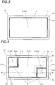
- FIG. 3 is a bottom view of FIG. 1 .
- FIG. 4 is a top view showing another example of the power module substrate of the present disclosure.
- FIG. 5 is a cross-sectional view taken along a line B-B of FIG. 4 .
- FIG. 6 is a bottom view of FIG. 4 .
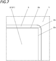
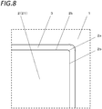
- FIG. 7 and FIG. 8 show examples of an enlarged view of a section A of FIG. 1 and FIG. 4 .
- FIG. 9 is a perspective view of FIG. 8 .
- a power module substrate 10 includes an insulating substrate 1 and metal plates 2 joined to main surfaces (upper and lower surfaces) of the insulating substrate 1 with brazing materials 3 in between.
- the surface roughness of the lateral surface of a metal plate 2 in its thickness direction is larger than the surface roughness of plane parts 2b sandwiching the corner part 2a.
- a space between brazing materials, with which the metal plates are joined to an insulating substrate also need to be reduced, and hence spread of the brazing materials from the lateral surfaces of the metal plates to the surface of the insulating substrate is also reduced.
- reducing spread of the brazing materials may lower joint reliability of the metal plates and the insulating substrate because thermal expansion difference between the metal plates and the insulating substrate may generate thermal stress, which may generate cracks in the brazing materials or the insulating substrate around, of the metal plates, corner parts where the thermal stress tends to concentrate.
- each metal plate 2 is located between the main surfaces (upper and lower surfaces) of the metal plate 2, and is substantially perpendicular to the both main surfaces (upper and lower surfaces). This can reduce a space between metal plates 2, and consequently produce the power module substrate 10 that is small.
- Each metal plate 2 is joined to the insulating substrate 1 with a brazing material 3.
- the brazing material 3 is interposed between the metal plate 2 and the insulating substrate 1.
- the brazing material 3 spreads from the lateral surface of the metal plate 2 to the surface of the insulating substrate 1, and forms a so-called meniscus-shaped fillet part.
- the fillet part of the brazing material 3 protrudes from the outer edge of the metal plate 2 in plan view. In order to reduce a space between metal plates 2, it is necessary to reduce the amounts of protrusion of brazing materials 3.
- heat generated in a semiconductor element when, for example, the semiconductor element is mounted on the power module substrate and it is operated as a power module generates the thermal stress due to thermal expansion difference between a metal plate(s) and an insulating substrate thereof.
- metal plates are often quadrangular in plan view, but the thermal stress tends to concentrate at the edge of each of such metal plates, in particular, immediately under corner parts thereof and at the outer end parts of a brazing material present around the corner parts.
- the amount of protrusion of the brazing material is a little, the corner parts of the metal plate and the end parts of the brazing material become close to one another, so that the thermal stress concentrates more.
- conventional power module substrates tend to have low joint reliability of metal plates and an insulating substrate.
- the surface roughness of each corner part 2a of the metal plate 2 is larger than the surface roughness of plane parts 2b sandwiching the corner part 2a, so that the corner parts 2a have lower wettability of the brazing material 3 than the plane parts 2b.
- the brazing material 3 climbs up the lateral surface of the metal plate 2 less at the corner parts 2a than at the plane parts 2b. Hence, the brazing material spreads much from the corner parts 2a onto the insulating substrate 1.
- a brazing material spreads onto an insulating substrate as indicated by a two-dot chain line in each of FIG. 7 and FIG. 8 .
- a corner part of a metal plate 2 and an end part of its brazing material 3 located outside the corner part have a long distance therebetween. This disperses the thermal stress, thereby improving the joint reliability of the metal plate 2 and the insulating substrate 1.
- the "corner parts 2a" herein are salient corner parts.
- three metal plates 2 (21, 22) composed of one relatively large metal plate 2 (21) and two small metal plates 2 (22) arranged so as to sandwich the relatively large metal plate 2 (21) are joined to the upper surface of the insulating substrate 1, and one metal plate 2 (23) is joined to the lower surface of the insulating substrate 1.
- all of these three metal plates 2 (21, 22) are quadrangular in plan view.
- the metal plate 2 (21) arranged at the center part of the upper surface of the insulating substrate 1 is shaped such that a pair of quadrangular corners on a diagonal is notched.
- a corner part 2c on the notch part in a section C enclosed by a broken line in FIG. 4 has a re-entrant corner.
- the two metal plates 22 located in the two notch parts each including the re-entrant corner part 2c are quadrangular.
- the large metal plate 2 (21) and the small metal plates 2 (22) are joined to the upper surface.
- an electronic component (s) is mounted on the large metal plate 2 (21), and an electrode(s) of the electronic component is electrically connected to the small metal plates 2 (22) by bonding wires.
- the thermal stress is large at the four corner parts 2a of the large quadrangular metal plate 2 (21) shown in FIG. 1 to FIG. 3 .
- unnotched corners on a diagonal of the large metal plate 2 (21) form the salient corner parts 2a where the thermal stress is large.
- the quadrangular metal plate 2 (23) joined to the lower surface of the insulating substrate 1 is also large, the four corners of this metal plate 2 (23) also form the corner parts 2a where the thermal stress is large.
- Each of these corner parts 2a is the corner part farthest from the center of its metal plate 2 in plan view.
- the center of the metal plate 2 in plan view may be referred to as the centroid of the shape of the metal plate 2 in plan view. Reducing the thermal stress at the corner parts 2a farthest from the center of the large metal plate 2 (21) among the metal plates 2 joined to the main surfaces (upper surface and lower surface) of the insulating substrate 1 is effective in improvement of the joint reliability. For that, the surface roughness of at least these corner parts 2a are larger than the surface roughness of the plane parts 2b sandwiching the corner parts 2a.
- Corner parts 22a of the small metal plates 2 (22) are close to the other metal plate 2 (21), and hence, in order for the brazing materials 3 not to spread much, the surface roughness of the corner parts 22a does not need to be large like the corner parts 2a.
- two salient corner parts 21a existing on the outer sides of each notch part and adjacent to the re-entrant corner part 2c are not of the corner part farthest from the center of the metal plate 2 but are close to either one of the other metal plates 2 (21), and hence the surface roughness of the corner parts 21a does not need to be large like the corner parts 2a either.
- the surface roughness of the lateral surface of each metal plate 2 is measured in the thickness direction of the metal plate 2 because the thickness direction of the metal plate 2, which is the climbing direction of the brazing material 3, affects degree of climbing of the brazing material 3 on the lateral surface of the metal plate 2.
- the surface roughness of each corner part 2a does not need to be the surface roughness at the apex of a corner, but is the surface roughness of a corner part being a range that has a predetermined width and includes the apex of a corner.
- the corner part is a part of up to about 0.5 mm from the apex of a corner in directions toward two plane parts 2b. When a corner is rounded in plan view as shown in FIG.
- a corner part is a part of up to about 0.5 mm from the apex of the corner in directions toward two plane parts 2b, where the apex is a point at which the two plane parts 2b extended in plan view intersect.
- the surface roughness of each plane part 2b is measured at a point(s) 2 mm or more away from a corner.
- the surface roughness of its plane parts 2b is measured at a point (s) 1.5 mm or more away from the respective ends of the rounded part.
- the surface roughness is the arithmetic mean roughness Ra, and may be measured with a laser microscope.
- the surface roughness may be measured with a laser microscope (KV9510) manufactured by Keyence Corporation under the following conditions: a measurement range of 100 ⁇ m; a cut-off of 0.08 mm; and a measurement pitch of 0.01 ⁇ m.
- the surface roughness is measured at multiple points (e.g. three points), and the mean is obtained as the surface roughness of the corner part 2a or the plane part 2b.
- a metal plate 2 is a copper plate and has a lateral surface formed by normal punching using a die (and additional processing), and its brazing material 3 contains a silver-copper alloy as a main component
- the surface roughness of each plane part 2b is, for example, 0.3 ⁇ m to 1.0 ⁇ m
- the surface roughness of each corner part 2a is, for example, 0.5 ⁇ m to 1.5 ⁇ m.
- the surface roughness of the plane part 2b and the surface roughness of the corner part 2a differ, for example, by 0.1 ⁇ m or more, the abovementioned effects are obtained.
- the brazing material 3 climbs up to about 1/5 to 1/2 of the thickness of the metal plate 2, and forms the concave meniscus-shaped fillet part from the lateral surface of the metal plate 2 to the upper surface of the insulating substrate 1, and the stress is likely to be relieved.
- the power module substrate 10 may be a power module substrate in which the surface roughness gradually increases from the plane parts 2b to the corner parts 2a.
- the power module substrate 10 may be a power module substrate in which the surface roughness becomes smaller as the points are away from the corner parts 2a toward the plane parts 2b.
- wettability of the brazing material on the lateral surface of the metal plate 2 changes gradually, and as shown in FIG. 9 , the height of the brazing material 3 on the lateral surface of the metal plate 2 changes gradually.
- the length of spread (protrusion width) of the brazing material 3 onto the insulating substrate 1 does not extremely differ between the plane parts 2b and the corner parts 2a.
- part where the length of spread changes is not shaped such that the thermal stress or the like tends to concentrate. Consequently, the joint reliability of the metal plate 2 and the insulating substrate 1 has improved.
- Change in the surface roughness from the plane parts 2b to the corner parts 2a in this case may be confirmed by measuring the surface roughness of the corner parts 2a and the plane parts 2b at regular intervals (e.g. 1 mm) .
- the surface roughness may not keep being smaller as the points are away from the corner parts 2a owing to variations in processing or measurement, the surface roughness is smaller as the points are away from the corner parts 2a in a fitted curve of a graph showing a relationship between the surface roughness and the measurement point (distance from each corner part 2a).
- the change may be confirmed as follows too: divide each plane part 2b into equal regions; measure the surface roughness at multiple points in each region; and compare the means of the surface roughness in the respective regions with one another.
- the corner parts 2a may be convex in plan view.
- the corner parts 2a may each do not have a jag and hence are shaped such that the stress is less likely to concentrate, cracks or the like are hardly generated in the brazing material 3 or the insulating substrate 1 starting from the vicinities of the corner parts 2a. Consequently, the reliability is high.
- the corner parts 2a may each be rounded and have a radius of about 0.1 mm to 3 mm in plan view, for example. Corner parts other than the corner parts 2a having the above surface roughness may also be convex.
- corner parts 22a of the small metal plates 22 examples include: the salient corner parts 22a of the small metal plates 22; and the salient corner parts 21a formed on the notch parts shown in FIG. 4 .
- a corner part adjacent to another metal plate 2 being convex reduces the possibility that, between the corner part and the adjacent metal plate 2, an electric discharge occurs and the insulation decreases.
- the surface roughness of the re-entrant corner parts 2c may be smaller than that of the plane parts 2b.
- the brazing material 3 climbs up more at the re-entrant corner parts 2c.
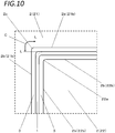
- the brazing material 3 spreads less from the re-entrant corner parts 2c onto the insulating substrate 1 than from the re-entrant corner parts 2c configured to have larger surface roughness (indicated by a two-dot chain line in FIG. 10 ).
- FIG. 10 shows an example of an enlarged view of the section C of FIG. 4(a) .
- FIG. 11 is a perspective view of FIG. 10 .
- the re-entrant corner parts 2c may be concave in plan view.
- the climbing height of the brazing material 3 at the re-entrant corner parts 2c tends to be higher.
- the re-entrant corner parts 2c each do not have a jag and hence are shaped such that the stress is less likely to concentrate, cracks or the like are hardly generated starting from the vicinities of the re-entrant corner parts 2c. Consequently, the reliability is high.
- the re-entrant corner parts 2c may each be concave and have a radius of about 0.1 mm to 3 mm in plan view, for example.
- the measurement point for the surface roughness of each re-entrant corner part 2c is in a part of up to about 0.5 mm from the apex of its corner in directions toward two plane parts 2b (21b).
- the measurement point is in a part of up to about 0.5 mm from the apex of the corner in directions toward two plane parts 2b (21b), where the apex is a point at which the two plane parts 2b (21b) extended in plan view intersect. More specifically, as shown in FIG. 10 , a range (range c shown in FIG. 10 and FIG. 11 ) sandwiched between points at which imaginary extension lines (two straight lines L shown in FIG.
- a range of a re-entrant corner part 2c is a range from the apex of its corner toward each of its plane parts 2b (21b) by the width of the brazing material 3 present outside the plane parts 2b (21b).
- the surface roughness may gradually increase from the re-entrant corner parts 2c to the plane parts 2b (21b).
- wettability of the brazing material on the lateral surface of the metal plate 2 changes gradually in the vicinities of the re-entrant corner parts 2c too, and as shown in FIG. 11 , the height of the brazing material 3 on the lateral surface of the metal plate 2 (21) changes gradually.
- the length of spread of the brazing material 3 onto the insulating substrate 1 does not extremely differ between the plane parts 2b (21b) and the re-entrant corner parts 2c. Hence, of the brazing material 3, part where the length of spread changes is not shaped such that the thermal stress or the like tends to concentrate.
- the surface roughness may gradually increase from the re-entrant corner parts 2c to the plane parts 2b and then to the corner parts 2a by being combined with the above-described case where the surface roughness gradually increases from the plane parts 2b to the corner parts 2a.
- FIG. 12 is a top view showing an example of a power module of the present disclosure.
- FIG. 13 is a cross-sectional view taken along a line B-B of FIG. 12 .
- a power module 100 includes the above-described power module substrate 10 and an electronic component 40 mounted on the metal plate 2 (21) of the power module substrate 10. According to the power module 100, because it includes the power module substrate 10 configured as described above, the power module 100 has high joint reliability of the metal plates 2 and the insulating substrate 1.
- the power module substrate 10 shown in FIG. 12 and FIG. 13 is the same as the power module substrate 10 shown in FIG. 1 to FIG. 3 , and includes one large metal plate 2 (21) and two small metal plates 2 (22) on the upper surface of the insulating substrate 1.
- the electronic component 40 is mounted on the large metal plate 2 (21), and electrically connected to the small metal plates 2 (22) by connective members, such as bonding wires 41.
- the metal plate 21 functions as a metal plate for mounting the electronic component 40 and dissipating heat
- the metal plates 22 function as terminals for electrically connecting the electronic component 40 to external electric circuit (s) (not shown), for example.
- the metal plates 22 may project from the outer edge of the insulating substrate 1 in plan view.
- the metal plate 23 is joined to the lower surface of the insulating substrate 1 with the brazing material 3.
- the metal plate 23 is quadrangular and slightly smaller than the lower surface of the insulating substrate 1. This metal plate 23 functions as a heat dissipating plate for releasing heat generated in the electronic component 40 to the outside of the power module 100, for example. This improves heat dissipation of the power module 100, and improves long-term operational reliability of the electronic component 40.
- the metal plate 23 joined to the lower surface of the insulating substrate 1 may function as a circuit board for mounting the electronic component 40 or connecting the electronic component 40 to an external circuit(s).
- the insulating substrate 1 is a base part for fixing and supporting the metal plates 2 in the power module substrate 10.
- the insulating substrate 1 functions as an insulating member for electrically insulating the metal plate 21 and the metal plates 22 on the upper surface of the insulating substrate 1 from one another, or the metal plates 21 and 22 on the upper surface of the insulating substrate 1 and the metal plate 23 on the lower surface of the insulating substrate 1 from one another.
- the insulating substrate 1 is made of a ceramic sintered body and has characteristics such as high mechanical strength and high heat transfer characteristics (cooling characteristics).
- a ceramic sintered body a known material may be used, and examples thereof include an alumina (Al 2 O 3 ) sintered body, an aluminum nitride (AlN) sintered body, a silicon nitride (Si 3 N 4 ) sintered body, and a silicon carbide (SiC) sintered body.
- a quadrangular plate having a length of 10 to 120 mm, a width of 10 to 120 mm, and a thickness of 0.2 to 3.0 mm may be used.
- Such an insulating substrate 1 may be manufactured with a known manufacturing method, for example, manufactured by: adding and mixing an organic binder or the like to and with base powder in which a sintering aid is added to alumina powder; shaping the resulting product into a substrate; and calcining the substrate.
- the metal plates 2 are each for mounting the electronic component 40, function as a circuit conductor that electrically connects the electronic component 40 to an external electric circuit, or function as a heat dissipating plate for dissipating heat generated in the electronic component 40.
- Their shapes are not particularly fixed, and are set to fit the wiring design of the power module 100.
- the thickness of the metal plates 2 may be set to, for example, 0.2 mm to 2.0 mm in terms of electrical resistance, strength, and heat dissipation.
- the number and arrangement of metal plates 2 are not limited to the examples shown in FIG. 1 to FIG. 3 and shown in FIG. 4 to FIG. 6 .
- the metal plates 2 are formed of a metal material, such as copper (Cu), a copper alloy, aluminum (Al), or an aluminum alloy. Pure copper or pure aluminum, which is 99% or more pure, has low electrical resistance and excellent thermal conductivity. When oxygen is contained as a component of the metal plates 2, a smaller content thereof in the metal plates 2 has an advantage in terms of improvement of the joint strength of the metal plates 2 and the bonding wires 41.
- the metal plates 2 may each be manufactured by, for example, punching a metal base substrate to be a predetermined shape, and performing additional processing for adjusting the surface roughness of the lateral surface. Normal punching using a die can produce a metal plate 2 having substantially right angles formed by the lateral surface and the main surfaces. This can make the distance between metal plates 2 short in the power module substrate 10, and consequently achieve the miniaturization.
- the shape of each metal plate 2 can be set by the shape of a die used for punching. In the same manner, the shape of the corner parts 2a and the shape of the re-entrant corner parts 2c can be made convex and concave in plan view, respectively.
- Performing additional processing on the lateral surface that has been formed by punching and where the surface roughness is relatively small can form the metal plate 2 having: the plane parts 2b the surface roughness of which is larger than that of the re-entrant corner parts 2c; and the salient corner parts 2a the surface roughness of which is larger than that of the plane parts 2b.
- Making degrees of additional processing, which is performed after punching, for the corner parts 2a, the plane parts 2b, and the re-entrant corner parts 2c different from one another makes degrees of the surface roughness thereof different from one another.
- additional processing usable include barreling and blasting.
- the abrasive hitting periods may be adjusted by the following method. For example, after barreling or blasting is performed in a state in which protective films made of resin or the like are provided on the plane parts 2b and the re-entrant corner parts 2c, barreling or blasting is performed again with the protective films removed, so that the surface roughness of the corner parts 2a is larger than that of the plane parts 2b and that of the re-entrant corner parts 2c.
- processing periods of the plane parts 2b and the re-entrant corner parts 2c may be set to be equal. Such additional processing can also remove burrs generated by punching. Further, punching and additional processing can chamfer the corners formed by the upper surface and the lateral surface of the metal plate 2, thereby forming an R plane, and consequently reduce electric discharges from the corners.
- the surface roughness of the re-entrant corner parts 2c that are less likely to be rubbed is unchanged, and the surface roughness of, for example, the plane parts 2b and the salient corner parts 2a that are likely to be rubbed becomes larger than that of the re-entrant corner parts 2c. Because the salient corner parts 2a are more likely to be hit by an abrasive than the plane parts 2b, the surface roughness of the salient corner parts 2a becomes larger than the surface roughness of the plane parts 2b by their processing periods being adjusted. The same applies to blasting, and hence the size of an abrasive may be adjusted.
- the surface roughness of the lateral surfaces of the small metal plates 22 does not need to be different from part to part.
- the small metal plates 22 and the plane parts 2b (21b) of the large metal plate 21 may be manufactured by the same additional processing as that performed on the plane parts 2b (21b) of the large metal plate 21.
- barreling or blasting may be performed using the above-described protective films.
- barreling or blasting is performed again with, of the protective films, part close to the corner parts 2a (21a) removed. This makes the processing amount (degree of rubbing) of additional processing different from part to part.
- the following may be repeated: perform additional processing with the re-entrant corner parts 2c and the plane parts 2b (21b) covered with protective films; and perform additional processing again with, of the protective films, part close to the corner parts 2a (21a) removed.
- multiple media having different sizes may be used.
- both the first media and the second media are unlikely to hit a portion of up to about 0.3 mm from the apex of the corner; the first media are likely but the second media are unlikely to hit a portion of up to about 1.5 mm from about 0.3 mm away from the apex of the corner; and both the first media and the second media are likely to hit a portion of about 1.5 mm or more away from the apex of the corner.
- the state of change in the surface roughness can be adjusted by the size, the number of sizes, the mixing ratio, and so forth of media to be combined. Media having different shapes and/or media having different materials can also be used in combination. The same applies to blasting.
- the metal plates 2 are joined (brazed) to the insulating substrate 1 with the brazing materials 3.
- the brazing materials 3 for example, when the metal plates 2 are made of copper (Cu) or a copper alloy, an active metal-containing brazing material in which an active metal, such as titanium (Ti), hafnium (Hf), or zirconium (Zr), is contained in a silver-copper (Ag-Cu) alloy brazing material may be used, whereas when the metal plates 2 are made of aluminum (Al) or an aluminum alloy, an aluminum-silicon (Al-Si) alloy brazing material or an aluminum-germanium (Al-Ge) alloy brazing material may be used.
- the metal plates 2 are joined (brazed) to the insulating substrate 1 by: applying a brazing material paste to the insulating substrate 1 with a method such as screen printing; placing the metal plates 2 thereon; and heating the resulting product in a pressurized state.
- the brazing materials 3 each spread from the outer edge of the metal plate 2 onto the insulating substrate 1 in plan view, and the spread width of the brazing material 3, namely the distance from the outer edge of the metal plate 2 to the outer edge of the brazing material 3 in plan view, is, for example, about 0.05 mm to 0.5 mm.
- the space between the metal plate 2 (21) and another metal plate 2 (22) is, for example, about 0.8 mm to 2.0 mm.
- the distance (space) between the outer edges of the brazing materials 3 present between the metal plates 2 adjacent to one another is, for example, 0.5 mm to 1.0 mm.
- the metal plate 23 on the lower surface of the insulating substrate 1 functions as a heat dissipating plate as described above
- the metal plate 23 on the lower surface may be set to have a size, in plan view, equal to or larger than the whole of the metal plates 2 (21 and 22) on the upper surface but smaller than the insulating substrate 1, for example.
- the metal plate 23 on the lower surface having about the same size as that defined by connecting the outer edges of the metal plates 2 (21 and 22) on the upper surface reduces thermal stress difference between the upper side and the lower side of the insulating substrate 1. This has an advantage in restraint of warpage of the power module substrate 10.
- the metal plate 23 on the lower surface being smaller than the insulating substrate 1 improves the electrical insulation between the metal plate 23 on the lower surface and the metal plates 2 (21 and 22) on the upper surface.
- the metal plate 23 on the lower surface being larger than the metal plates 2 (21 and 22) on the upper surface, namely the outer edge of the metal plate 23 being located outside the outer edge of the metal plates 2 (21 and 22) on the upper surface in see-through plan view, effectively diffuses heat in the horizontal direction of the metal plate 23 on the lower surface, the heat being generated during use of the power module 100. This has an advantage in improvement of heat dissipation.
- the metal plate 23 on the lower surface may be made larger than the insulating substrate 1. In this case, the metal plates 2 (21 and 22) on the upper surface are joined to the insulating substrate 1 so as to be located inside the outer edge of the insulating substrate 1, and hence certainly insulated from the metal plate 23 on the lower surface.
- plating layers may be formed to protect the surfaces or to improve the joining property of the brazing materials 3, the bonding wires 41, and so forth.
- the plating layers may each be a metal plating layer of palladium, nickel, silver, or the like.
- the power module substrate 10 may be manufactured as follows: manufacture a product with a so-called multi-cavity form; and divide the product.
- the electronic component 40 is, for example, a power semiconductor device, such as an IGBT.
- the electronic component 40 is joined and fixed to a metal plate 2 by, for example, soldering, brazing or diffusion bonding.
- the electronic component 40 is fixed to the large metal plate 21 joined to the upper surface of the insulating substrate 1, and is electrically connected to the small metal plates 22 on the upper surface by the bonding wires 41 made of aluminum, gold (Au), or the like.
- the power module 100 may be, for example, housed in a case, or housed in a case and covered with resin.
- a heat sink may be arranged, and the metal plate 23 on the lower surface of the power module substrate 10 and the heat sink may be joined to one another with a heat-transfer material, for example, heat-transfer grease, to enhance heat dissipation.
- a heat-transfer material for example, heat-transfer grease
- the power module substrate 10 and the power module 100 are not limited to the examples described in the above embodiment, and can be variously modified within the scope of the present disclosure.
Landscapes
- Engineering & Computer Science (AREA)
- Chemical & Material Sciences (AREA)
- Ceramic Engineering (AREA)
- Materials Engineering (AREA)
- Structural Engineering (AREA)
- Organic Chemistry (AREA)
- Manufacturing & Machinery (AREA)
- Microelectronics & Electronic Packaging (AREA)
- Cooling Or The Like Of Semiconductors Or Solid State Devices (AREA)
- Structure Of Printed Boards (AREA)
- Manufacturing Of Printed Wiring (AREA)
Abstract
Description
- The present disclosure relates to: a power module substrate in which metal plates are joined to an insulating substrate; and a power module.
- As a circuit board that is used in an electronic device, such as a power module equipped with an electronic component(s) exemplified by an IGBT (Insulated Gate Bipolar Transistor), there has been used a power module substrate in which metal plates made of a metal material, such as copper, are joined to an insulating substrate made of a ceramic sintered body or the like.
- In order to miniaturize a power module, metal plates are each manufactured by punching to have a lateral surface perpendicular to an insulating substrate, thereby reducing a space between (the lateral surfaces of) metal plates. (See, for example,
Patent Literature 1.) - Patent Literature 1:
JP 2007-53349 A - A power module substrate according to an aspect of the present disclosure includes: an insulating substrate; and a metal plate joined to the insulating substrate with a brazing material in between, wherein as to surface roughness of a lateral surface of the metal plate in a thickness direction, the surface roughness of at least a corner part farthest from a center of the metal plate in plan view is larger than the surface roughness of plane parts sandwiching the corner part.
- A power module according to an aspect of the present disclosure includes: the above power module substrate; and an electronic component mounted on the metal plate of the power module substrate.
- According to the power module substrate of the present disclosure, because it is configured as described above, the brazing material is restrained from climbing up at the corner part, where thermal stress tends to concentrate, and spreads much from the corner part onto the insulating substrate, so that the power module substrate has excellent joint reliability of the metal plate and the insulating substrate.
- According to the power module of the present disclosure, because it includes the power module substrate configured as described above, the power module has high reliability.
-
-
FIG. 1 is a top view showing an example of a power module substrate of the present disclosure. -
FIG. 2 is a cross-sectional view taken along a line B-B ofFIG. 1 . -
FIG. 3 is a bottom view ofFIG. 1 . -
FIG. 4 is a top view showing another example of the power module substrate of the present disclosure. -
FIG. 5 is a cross-sectional view taken along a line B-B ofFIG. 4 . -
FIG. 6 is a bottom view ofFIG. 4 . -
FIG. 7 shows an example of an enlarged view of a section A ofFIG. 1 andFIG. 4 . -
FIG. 8 shows another example of the enlarged view of the section A ofFIG. 1 andFIG. 4 . -
FIG. 9 is a perspective view ofFIG. 8 . -
FIG. 10 shows an example of an enlarged view of a section C ofFIG. 4 . -
FIG. 11 is a perspective view ofFIG. 10 . -
FIG. 12 is a top view showing an example of a power module of the present disclosure. -
FIG. 13 is a cross-sectional view taken along a line B-B ofFIG. 12 . - A power module substrate and a power module according to an embodiment of the present disclosure will be described with reference to the drawings. It is noted that "upper" and "lower" are used in the following description for the sake of convenience, and hence not intended to limit the upper and lower sides in actual use of the power module substrate, the power module, or the like.
-
FIG. 1 is a top view showing an example of a power module substrate of the present disclosure.FIG. 2 is a cross-sectional view taken along a line B-B ofFIG. 1 .FIG. 3 is a bottom view ofFIG. 1 .FIG. 4 is a top view showing another example of the power module substrate of the present disclosure.FIG. 5 is a cross-sectional view taken along a line B-B ofFIG. 4 .FIG. 6 is a bottom view ofFIG. 4 .FIG. 7 andFIG. 8 show examples of an enlarged view of a section A ofFIG. 1 andFIG. 4 .FIG. 9 is a perspective view ofFIG. 8 . - A
power module substrate 10 includes aninsulating substrate 1 andmetal plates 2 joined to main surfaces (upper and lower surfaces) of theinsulating substrate 1 with brazingmaterials 3 in between. As to surface roughness of the lateral surface of ametal plate 2 in its thickness direction, the surface roughness of at least a corner part(s) 2a farthest from the center of themetal plate 2 in plan view is larger than the surface roughness ofplane parts 2b sandwiching thecorner part 2a. - In a conventional power module substrate, in order to reduce a space between metal plates, a space between brazing materials, with which the metal plates are joined to an insulating substrate, also need to be reduced, and hence spread of the brazing materials from the lateral surfaces of the metal plates to the surface of the insulating substrate is also reduced. However, reducing spread of the brazing materials may lower joint reliability of the metal plates and the insulating substrate because thermal expansion difference between the metal plates and the insulating substrate may generate thermal stress, which may generate cracks in the brazing materials or the insulating substrate around, of the metal plates, corner parts where the thermal stress tends to concentrate.
- The lateral surface of each
metal plate 2 is located between the main surfaces (upper and lower surfaces) of themetal plate 2, and is substantially perpendicular to the both main surfaces (upper and lower surfaces). This can reduce a space betweenmetal plates 2, and consequently produce thepower module substrate 10 that is small. Eachmetal plate 2 is joined to theinsulating substrate 1 with abrazing material 3. Thebrazing material 3 is interposed between themetal plate 2 and theinsulating substrate 1. The brazingmaterial 3 spreads from the lateral surface of themetal plate 2 to the surface of theinsulating substrate 1, and forms a so-called meniscus-shaped fillet part. The fillet part of thebrazing material 3 protrudes from the outer edge of themetal plate 2 in plan view. In order to reduce a space betweenmetal plates 2, it is necessary to reduce the amounts of protrusion of brazingmaterials 3. - In a power module substrate, heat generated in a semiconductor element when, for example, the semiconductor element is mounted on the power module substrate and it is operated as a power module generates the thermal stress due to thermal expansion difference between a metal plate(s) and an insulating substrate thereof. For example, metal plates are often quadrangular in plan view, but the thermal stress tends to concentrate at the edge of each of such metal plates, in particular, immediately under corner parts thereof and at the outer end parts of a brazing material present around the corner parts. When the amount of protrusion of the brazing material is a little, the corner parts of the metal plate and the end parts of the brazing material become close to one another, so that the thermal stress concentrates more. Thus, conventional power module substrates tend to have low joint reliability of metal plates and an insulating substrate.
- According to the
power module substrate 10 of the present disclosure, as to the surface roughness of the lateral surface of ametal plate 2 in its thickness direction, the surface roughness of eachcorner part 2a of themetal plate 2 is larger than the surface roughness ofplane parts 2b sandwiching thecorner part 2a, so that thecorner parts 2a have lower wettability of thebrazing material 3 than theplane parts 2b. The brazingmaterial 3 climbs up the lateral surface of themetal plate 2 less at thecorner parts 2a than at theplane parts 2b. Hence, the brazing material spreads much from thecorner parts 2a onto theinsulating substrate 1. For example, in the vicinity of a corner part in a conventional power module substrate, which is uniform in surface roughness, a brazing material spreads onto an insulating substrate as indicated by a two-dot chain line in each ofFIG. 7 andFIG. 8 . As compared with such a conventional one, a corner part of ametal plate 2 and an end part of itsbrazing material 3 located outside the corner part have a long distance therebetween. This disperses the thermal stress, thereby improving the joint reliability of themetal plate 2 and theinsulating substrate 1. - The "
corner parts 2a" herein are salient corner parts. In each of examples shown inFIG. 1 to FIG. 3 and shown inFIG. 4 to FIG. 6 , three metal plates 2 (21, 22) composed of one relatively large metal plate 2 (21) and two small metal plates 2 (22) arranged so as to sandwich the relatively large metal plate 2 (21) are joined to the upper surface of theinsulating substrate 1, and one metal plate 2 (23) is joined to the lower surface of theinsulating substrate 1. In the example shown inFIG. 1 to FIG. 3 , all of these three metal plates 2 (21, 22) are quadrangular in plan view. On the other hand, in the example shown inFIG. 4 to FIG. 6 , the metal plate 2 (21) arranged at the center part of the upper surface of theinsulating substrate 1 is shaped such that a pair of quadrangular corners on a diagonal is notched. Acorner part 2c on the notch part in a section C enclosed by a broken line inFIG. 4 has a re-entrant corner. The twometal plates 22 located in the two notch parts each including there-entrant corner part 2c are quadrangular. - It is unnecessary for the surface roughness of all salient corner parts to be larger than the surface roughness of plane parts, as long as the surface roughness of at least a corner part (s) 2a farthest from the center of its
metal plate 2 in plan view is larger than the surface roughness ofplane parts 2b sandwiching thecorner part 2a. As described above, in each of the examples shown inFIG. 1 to FIG. 3 and shown inFIG. 4 to FIG. 6 , the large metal plate 2 (21) and the small metal plates 2 (22) are joined to the upper surface. For example, an electronic component (s) is mounted on the large metal plate 2 (21), and an electrode(s) of the electronic component is electrically connected to the small metal plates 2 (22) by bonding wires. Because the above-described thermal stress is larger as the joint length of ametal plate 2 and the insulatingsubstrate 1 is longer, the thermal stress is large at the fourcorner parts 2a of the large quadrangular metal plate 2 (21) shown inFIG. 1 to FIG. 3 . In the example shown inFIG. 4 to FIG. 6 , unnotched corners on a diagonal of the large metal plate 2 (21) form thesalient corner parts 2a where the thermal stress is large. Further, because the quadrangular metal plate 2 (23) joined to the lower surface of the insulatingsubstrate 1 is also large, the four corners of this metal plate 2 (23) also form thecorner parts 2a where the thermal stress is large. Each of thesecorner parts 2a is the corner part farthest from the center of itsmetal plate 2 in plan view. The center of themetal plate 2 in plan view may be referred to as the centroid of the shape of themetal plate 2 in plan view. Reducing the thermal stress at thecorner parts 2a farthest from the center of the large metal plate 2 (21) among themetal plates 2 joined to the main surfaces (upper surface and lower surface) of the insulatingsubstrate 1 is effective in improvement of the joint reliability. For that, the surface roughness of at least thesecorner parts 2a are larger than the surface roughness of theplane parts 2b sandwiching thecorner parts 2a. -
Corner parts 22a of the small metal plates 2 (22) are close to the other metal plate 2 (21), and hence, in order for thebrazing materials 3 not to spread much, the surface roughness of thecorner parts 22a does not need to be large like thecorner parts 2a. Further, in the example shown inFIG. 4 to FIG. 6 , twosalient corner parts 21a existing on the outer sides of each notch part and adjacent to there-entrant corner part 2c are not of the corner part farthest from the center of themetal plate 2 but are close to either one of the other metal plates 2 (21), and hence the surface roughness of thecorner parts 21a does not need to be large like thecorner parts 2a either. In the example shown inFIG. 4 to FIG. 6 , when the notch parts keep their sizes but thesmall metal plates 22 are smaller, so that thesalient corner parts 21a on the notch parts of thelarge metal plate 21 are sufficiently far away from thesmall metal plates 22, the surface roughness of thesalient corner parts 21a on the notch parts may be large like thecorner parts 2a. - The surface roughness of the lateral surface of each
metal plate 2 is measured in the thickness direction of themetal plate 2 because the thickness direction of themetal plate 2, which is the climbing direction of thebrazing material 3, affects degree of climbing of thebrazing material 3 on the lateral surface of themetal plate 2. The surface roughness of eachcorner part 2a does not need to be the surface roughness at the apex of a corner, but is the surface roughness of a corner part being a range that has a predetermined width and includes the apex of a corner. The corner part is a part of up to about 0.5 mm from the apex of a corner in directions toward twoplane parts 2b. When a corner is rounded in plan view as shown inFIG. 8 , a corner part is a part of up to about 0.5 mm from the apex of the corner in directions toward twoplane parts 2b, where the apex is a point at which the twoplane parts 2b extended in plan view intersect. The surface roughness of eachplane part 2b is measured at a point(s) 2 mm or more away from a corner. When acorner part 2a is rounded, and its radius is larger than 0.5 mm, the surface roughness of itsplane parts 2b is measured at a point (s) 1.5 mm or more away from the respective ends of the rounded part. - The surface roughness is the arithmetic mean roughness Ra, and may be measured with a laser microscope. For example, the surface roughness may be measured with a laser microscope (KV9510) manufactured by Keyence Corporation under the following conditions: a measurement range of 100 µm; a cut-off of 0.08 mm; and a measurement pitch of 0.01 µm. In each of the above-defined corner part(s) 2a and plane part(s) 2b, the surface roughness is measured at multiple points (e.g. three points), and the mean is obtained as the surface roughness of the
corner part 2a or theplane part 2b. For example, when ametal plate 2 is a copper plate and has a lateral surface formed by normal punching using a die (and additional processing), and itsbrazing material 3 contains a silver-copper alloy as a main component, the surface roughness of eachplane part 2b is, for example, 0.3 µm to 1.0 µm, and the surface roughness of eachcorner part 2a is, for example, 0.5 µm to 1.5 µm. When the surface roughness of theplane part 2b and the surface roughness of thecorner part 2a differ, for example, by 0.1 µm or more, the abovementioned effects are obtained. Further, when the surface roughness are in the above ranges, even at thecorner parts 2a, thebrazing material 3 climbs up to about 1/5 to 1/2 of the thickness of themetal plate 2, and forms the concave meniscus-shaped fillet part from the lateral surface of themetal plate 2 to the upper surface of the insulatingsubstrate 1, and the stress is likely to be relieved. - The
power module substrate 10 may be a power module substrate in which the surface roughness gradually increases from theplane parts 2b to thecorner parts 2a. In other words, thepower module substrate 10 may be a power module substrate in which the surface roughness becomes smaller as the points are away from thecorner parts 2a toward theplane parts 2b. In this case, wettability of the brazing material on the lateral surface of themetal plate 2 changes gradually, and as shown inFIG. 9 , the height of thebrazing material 3 on the lateral surface of themetal plate 2 changes gradually. The length of spread (protrusion width) of thebrazing material 3 onto the insulatingsubstrate 1 does not extremely differ between theplane parts 2b and thecorner parts 2a. Hence, of thebrazing material 3, part where the length of spread changes is not shaped such that the thermal stress or the like tends to concentrate. Consequently, the joint reliability of themetal plate 2 and the insulatingsubstrate 1 has improved. - Change in the surface roughness from the
plane parts 2b to thecorner parts 2a in this case may be confirmed by measuring the surface roughness of thecorner parts 2a and theplane parts 2b at regular intervals (e.g. 1 mm) . Although the surface roughness may not keep being smaller as the points are away from thecorner parts 2a owing to variations in processing or measurement, the surface roughness is smaller as the points are away from thecorner parts 2a in a fitted curve of a graph showing a relationship between the surface roughness and the measurement point (distance from eachcorner part 2a). The change may be confirmed as follows too: divide eachplane part 2b into equal regions; measure the surface roughness at multiple points in each region; and compare the means of the surface roughness in the respective regions with one another. - As described above, as shown in
FIG. 8 andFIG. 9 , thecorner parts 2a may be convex in plan view. In this case, because thecorner parts 2a each do not have a jag and hence are shaped such that the stress is less likely to concentrate, cracks or the like are hardly generated in thebrazing material 3 or the insulatingsubstrate 1 starting from the vicinities of thecorner parts 2a. Consequently, the reliability is high. Thecorner parts 2a may each be rounded and have a radius of about 0.1 mm to 3 mm in plan view, for example. Corner parts other than thecorner parts 2a having the above surface roughness may also be convex. Examples of the other corner parts include: thesalient corner parts 22a of thesmall metal plates 22; and thesalient corner parts 21a formed on the notch parts shown inFIG. 4 . A corner part adjacent to anothermetal plate 2 being convex reduces the possibility that, between the corner part and theadjacent metal plate 2, an electric discharge occurs and the insulation decreases. - As shown in
FIG. 4 , when ametal plate 2 hasre-entrant corner parts 2c, and other metal plates 2 (22) are located near the respectivere-entrant corner parts 2c, the surface roughness of there-entrant corner parts 2c may be smaller than that of theplane parts 2b. In this case, as shown inFIG. 11 , thebrazing material 3 climbs up more at there-entrant corner parts 2c. Hence, thebrazing material 3 spreads less from there-entrant corner parts 2c onto the insulatingsubstrate 1 than from there-entrant corner parts 2c configured to have larger surface roughness (indicated by a two-dot chain line inFIG. 10 ). This reduces the possibility that the distances between thebrazing material 3 and theother metal plates 2 arranged close to the respectivere-entrant corner parts 2c become short and the insulation decreases.FIG. 10 shows an example of an enlarged view of the section C ofFIG. 4(a) .FIG. 11 is a perspective view ofFIG. 10 . - As shown in
FIG. 10 andFIG. 11 , there-entrant corner parts 2c may be concave in plan view. In this case, the climbing height of thebrazing material 3 at there-entrant corner parts 2c tends to be higher. Further, because there-entrant corner parts 2c each do not have a jag and hence are shaped such that the stress is less likely to concentrate, cracks or the like are hardly generated starting from the vicinities of there-entrant corner parts 2c. Consequently, the reliability is high. There-entrant corner parts 2c may each be concave and have a radius of about 0.1 mm to 3 mm in plan view, for example. - The measurement point for the surface roughness of each
re-entrant corner part 2c is in a part of up to about 0.5 mm from the apex of its corner in directions toward twoplane parts 2b (21b). When a corner is rounded in plan view as shown inFIG. 10 andFIG. 11 , the measurement point is in a part of up to about 0.5 mm from the apex of the corner in directions toward twoplane parts 2b (21b), where the apex is a point at which the twoplane parts 2b (21b) extended in plan view intersect. More specifically, as shown inFIG. 10 , a range (range c shown inFIG. 10 andFIG. 11 ) sandwiched between points at which imaginary extension lines (two straight lines L shown inFIG. 10 ) intersect with the lateral surface of the metal plate 2 (21) having a re-entrant corner part(s) 2c is defined as there-entrant corner part 2c of themetal plate 21, where the imaginary extension lines are obtained by extending, in directions toward the corner of there-entrant corner part 2c, straight-line parts of the outer peripheral edge of thebrazing material 3 that spreads outward from theplane parts 2b (21b) of the metal plate 2 (21) having there-entrant corner part 2c. In other words, a range of are-entrant corner part 2c is a range from the apex of its corner toward each of itsplane parts 2b (21b) by the width of thebrazing material 3 present outside theplane parts 2b (21b). - The surface roughness may gradually increase from the
re-entrant corner parts 2c to theplane parts 2b (21b). In this case, wettability of the brazing material on the lateral surface of themetal plate 2 changes gradually in the vicinities of there-entrant corner parts 2c too, and as shown inFIG. 11 , the height of thebrazing material 3 on the lateral surface of the metal plate 2 (21) changes gradually. The length of spread of thebrazing material 3 onto the insulatingsubstrate 1 does not extremely differ between theplane parts 2b (21b) and there-entrant corner parts 2c. Hence, of thebrazing material 3, part where the length of spread changes is not shaped such that the thermal stress or the like tends to concentrate. Consequently, the joint reliability of the metal plate 2 (21) and the insulatingsubstrate 1 has improved. The surface roughness may gradually increase from there-entrant corner parts 2c to theplane parts 2b and then to thecorner parts 2a by being combined with the above-described case where the surface roughness gradually increases from theplane parts 2b to thecorner parts 2a. -
FIG. 12 is a top view showing an example of a power module of the present disclosure.FIG. 13 is a cross-sectional view taken along a line B-B ofFIG. 12 . As shown inFIG. 12 and FIG. 13 , apower module 100 includes the above-describedpower module substrate 10 and anelectronic component 40 mounted on the metal plate 2 (21) of thepower module substrate 10. According to thepower module 100, because it includes thepower module substrate 10 configured as described above, thepower module 100 has high joint reliability of themetal plates 2 and the insulatingsubstrate 1. - The
power module substrate 10 shown inFIG. 12 and FIG. 13 is the same as thepower module substrate 10 shown inFIG. 1 to FIG. 3 , and includes one large metal plate 2 (21) and two small metal plates 2 (22) on the upper surface of the insulatingsubstrate 1. Theelectronic component 40 is mounted on the large metal plate 2 (21), and electrically connected to the small metal plates 2 (22) by connective members, such asbonding wires 41. In the example shown inFIG. 12 and FIG. 13 , themetal plate 21 functions as a metal plate for mounting theelectronic component 40 and dissipating heat, and themetal plates 22 function as terminals for electrically connecting theelectronic component 40 to external electric circuit (s) (not shown), for example. In this case, themetal plates 22 may project from the outer edge of the insulatingsubstrate 1 in plan view. In each of the examples shown inFIG. 1 to FIG. 3 and shown inFIG. 4 to FIG. 6 , themetal plate 23 is joined to the lower surface of the insulatingsubstrate 1 with thebrazing material 3. In each of the examples shown inFIG. 1 to FIG. 3 and shown inFIG. 4 to FIG. 6 , themetal plate 23 is quadrangular and slightly smaller than the lower surface of the insulatingsubstrate 1. Thismetal plate 23 functions as a heat dissipating plate for releasing heat generated in theelectronic component 40 to the outside of thepower module 100, for example. This improves heat dissipation of thepower module 100, and improves long-term operational reliability of theelectronic component 40. Themetal plate 23 joined to the lower surface of the insulatingsubstrate 1 may function as a circuit board for mounting theelectronic component 40 or connecting theelectronic component 40 to an external circuit(s). - The insulating
substrate 1 is a base part for fixing and supporting themetal plates 2 in thepower module substrate 10. The insulatingsubstrate 1 functions as an insulating member for electrically insulating themetal plate 21 and themetal plates 22 on the upper surface of the insulatingsubstrate 1 from one another, or themetal plates substrate 1 and themetal plate 23 on the lower surface of the insulatingsubstrate 1 from one another. - Preferably, the insulating
substrate 1 is made of a ceramic sintered body and has characteristics such as high mechanical strength and high heat transfer characteristics (cooling characteristics). As the ceramic sintered body, a known material may be used, and examples thereof include an alumina (Al2O3) sintered body, an aluminum nitride (AlN) sintered body, a silicon nitride (Si3N4) sintered body, and a silicon carbide (SiC) sintered body. As the insulatingsubstrate 1, for example, a quadrangular plate having a length of 10 to 120 mm, a width of 10 to 120 mm, and a thickness of 0.2 to 3.0 mm may be used. Such an insulatingsubstrate 1 may be manufactured with a known manufacturing method, for example, manufactured by: adding and mixing an organic binder or the like to and with base powder in which a sintering aid is added to alumina powder; shaping the resulting product into a substrate; and calcining the substrate. - As described above, in the
power module 100, themetal plates 2 are each for mounting theelectronic component 40, function as a circuit conductor that electrically connects theelectronic component 40 to an external electric circuit, or function as a heat dissipating plate for dissipating heat generated in theelectronic component 40. Their shapes are not particularly fixed, and are set to fit the wiring design of thepower module 100. The thickness of themetal plates 2 may be set to, for example, 0.2 mm to 2.0 mm in terms of electrical resistance, strength, and heat dissipation. The number and arrangement ofmetal plates 2 are not limited to the examples shown inFIG. 1 to FIG. 3 and shown inFIG. 4 to FIG. 6 . - The
metal plates 2 are formed of a metal material, such as copper (Cu), a copper alloy, aluminum (Al), or an aluminum alloy. Pure copper or pure aluminum, which is 99% or more pure, has low electrical resistance and excellent thermal conductivity. When oxygen is contained as a component of themetal plates 2, a smaller content thereof in themetal plates 2 has an advantage in terms of improvement of the joint strength of themetal plates 2 and thebonding wires 41. - The
metal plates 2 may each be manufactured by, for example, punching a metal base substrate to be a predetermined shape, and performing additional processing for adjusting the surface roughness of the lateral surface. Normal punching using a die can produce ametal plate 2 having substantially right angles formed by the lateral surface and the main surfaces. This can make the distance betweenmetal plates 2 short in thepower module substrate 10, and consequently achieve the miniaturization. The shape of eachmetal plate 2 can be set by the shape of a die used for punching. In the same manner, the shape of thecorner parts 2a and the shape of there-entrant corner parts 2c can be made convex and concave in plan view, respectively. - Performing additional processing on the lateral surface that has been formed by punching and where the surface roughness is relatively small can form the
metal plate 2 having: theplane parts 2b the surface roughness of which is larger than that of there-entrant corner parts 2c; and thesalient corner parts 2a the surface roughness of which is larger than that of theplane parts 2b. Making degrees of additional processing, which is performed after punching, for thecorner parts 2a, theplane parts 2b, and there-entrant corner parts 2c different from one another makes degrees of the surface roughness thereof different from one another. Examples of additional processing usable include barreling and blasting. In blasting, periods of an abrasive hitting there-entrant corner parts 2c, theplane parts 2b, and thesalient corner parts 2a are made longer in this order. In either of barreling and blasting, the abrasive hitting periods may be adjusted by the following method. For example, after barreling or blasting is performed in a state in which protective films made of resin or the like are provided on theplane parts 2b and there-entrant corner parts 2c, barreling or blasting is performed again with the protective films removed, so that the surface roughness of thecorner parts 2a is larger than that of theplane parts 2b and that of there-entrant corner parts 2c. Because there-entrant corner parts 2c are less likely to be hit by an abrasive than theplane parts 2b, processing periods of theplane parts 2b and there-entrant corner parts 2c may be set to be equal. Such additional processing can also remove burrs generated by punching. Further, punching and additional processing can chamfer the corners formed by the upper surface and the lateral surface of themetal plate 2, thereby forming an R plane, and consequently reduce electric discharges from the corners. - In order for additional processing to make the surface roughness of the
re-entrant corner parts 2c smaller than the surface roughness of theplane parts 2b, there is a usable method of, for example, adjusting the size of media (abrasive stone or abrasive) used for barreling such that the abrasive is unlikely to hit there-entrant corner parts 2c. For example, when media each having a diameter of 0.6 mm are used, in eachre-entrant corner part 2c that is right-angled, the media are unlikely to hit a portion of up to about 0.3 mm from the apex of the corner, so that this portion is unlikely to be rubbed, and the other portions are likely to be rubbed. In the case of the rubbing that increases the surface roughness, the surface roughness of there-entrant corner parts 2c that are less likely to be rubbed is unchanged, and the surface roughness of, for example, theplane parts 2b and thesalient corner parts 2a that are likely to be rubbed becomes larger than that of there-entrant corner parts 2c. Because thesalient corner parts 2a are more likely to be hit by an abrasive than theplane parts 2b, the surface roughness of thesalient corner parts 2a becomes larger than the surface roughness of theplane parts 2b by their processing periods being adjusted. The same applies to blasting, and hence the size of an abrasive may be adjusted. - The surface roughness of the lateral surfaces of the
small metal plates 22 does not need to be different from part to part. However, in order for thesmall metal plates 22 and theplane parts 2b (21b) of thelarge metal plate 21 to have the same degree of climbing of thebrazing materials 3 onto the lateral surfaces and the same degree of spread of thebrazing materials 3 onto the insulatingsubstrate 1, thesmall metal plates 22 may be manufactured by the same additional processing as that performed on theplane parts 2b (21b) of thelarge metal plate 21. - In order for the surface roughness of the lateral surface of the
metal plate 2 to gradually increase from theplane parts 2b to thecorner parts 2a, for example, barreling or blasting may be performed using the above-described protective films. For example, after barreling or blasting is performed in a state in which theplane parts 2b are covered with protective films, barreling or blasting is performed again with, of the protective films, part close to thecorner parts 2a (21a) removed. This makes the processing amount (degree of rubbing) of additional processing different from part to part. - In order for the surface roughness to gradually increase from the
re-entrant corner parts 2c to theplane parts 2b (21b) and then to thecorner parts 2a (21a), the following may be repeated: perform additional processing with there-entrant corner parts 2c and theplane parts 2b (21b) covered with protective films; and perform additional processing again with, of the protective films, part close to thecorner parts 2a (21a) removed. In barreling described above, multiple media having different sizes may be used. For example, when second media each having a diameter of 3 mm are used in addition to first media each having a diameter of 0.6 mm, which are described above, in eachre-entrant corner part 2c, both the first media and the second media are unlikely to hit a portion of up to about 0.3 mm from the apex of the corner; the first media are likely but the second media are unlikely to hit a portion of up to about 1.5 mm from about 0.3 mm away from the apex of the corner; and both the first media and the second media are likely to hit a portion of about 1.5 mm or more away from the apex of the corner. As the portion is away from there-entrant corner part 2c, more media hit the portion, and the portion is rubbed accordingly, which gradually increases the surface roughness. The state of change in the surface roughness can be adjusted by the size, the number of sizes, the mixing ratio, and so forth of media to be combined. Media having different shapes and/or media having different materials can also be used in combination. The same applies to blasting. - The
metal plates 2 are joined (brazed) to the insulatingsubstrate 1 with thebrazing materials 3. As thebrazing materials 3, for example, when themetal plates 2 are made of copper (Cu) or a copper alloy, an active metal-containing brazing material in which an active metal, such as titanium (Ti), hafnium (Hf), or zirconium (Zr), is contained in a silver-copper (Ag-Cu) alloy brazing material may be used, whereas when themetal plates 2 are made of aluminum (Al) or an aluminum alloy, an aluminum-silicon (Al-Si) alloy brazing material or an aluminum-germanium (Al-Ge) alloy brazing material may be used. Themetal plates 2 are joined (brazed) to the insulatingsubstrate 1 by: applying a brazing material paste to the insulatingsubstrate 1 with a method such as screen printing; placing themetal plates 2 thereon; and heating the resulting product in a pressurized state. - The
brazing materials 3 each spread from the outer edge of themetal plate 2 onto the insulatingsubstrate 1 in plan view, and the spread width of thebrazing material 3, namely the distance from the outer edge of themetal plate 2 to the outer edge of thebrazing material 3 in plan view, is, for example, about 0.05 mm to 0.5 mm. The space between the metal plate 2 (21) and another metal plate 2 (22) is, for example, about 0.8 mm to 2.0 mm. The distance (space) between the outer edges of thebrazing materials 3 present between themetal plates 2 adjacent to one another is, for example, 0.5 mm to 1.0 mm. When the spaces between thebrazing materials 3 and between themetal plates 2 are in the above ranges, the possibility of poor insulation between themetal plates 2 adjacent to one another is reduced. Also, because the spaces are sufficiently small, thepower module substrate 10 and thepower module 100 can be made small. - When the
metal plate 23 on the lower surface of the insulatingsubstrate 1 functions as a heat dissipating plate as described above, themetal plate 23 on the lower surface may be set to have a size, in plan view, equal to or larger than the whole of the metal plates 2 (21 and 22) on the upper surface but smaller than the insulatingsubstrate 1, for example. Themetal plate 23 on the lower surface having about the same size as that defined by connecting the outer edges of the metal plates 2 (21 and 22) on the upper surface reduces thermal stress difference between the upper side and the lower side of the insulatingsubstrate 1. This has an advantage in restraint of warpage of thepower module substrate 10. Themetal plate 23 on the lower surface being smaller than the insulatingsubstrate 1 improves the electrical insulation between themetal plate 23 on the lower surface and the metal plates 2 (21 and 22) on the upper surface. Themetal plate 23 on the lower surface being larger than the metal plates 2 (21 and 22) on the upper surface, namely the outer edge of themetal plate 23 being located outside the outer edge of the metal plates 2 (21 and 22) on the upper surface in see-through plan view, effectively diffuses heat in the horizontal direction of themetal plate 23 on the lower surface, the heat being generated during use of thepower module 100. This has an advantage in improvement of heat dissipation. When it is desired to further improve the heat dissipation, themetal plate 23 on the lower surface may be made larger than the insulatingsubstrate 1. In this case, the metal plates 2 (21 and 22) on the upper surface are joined to the insulatingsubstrate 1 so as to be located inside the outer edge of the insulatingsubstrate 1, and hence certainly insulated from themetal plate 23 on the lower surface. - On the surfaces of the metal plates 2 (21, 22, 23), plating layers may be formed to protect the surfaces or to improve the joining property of the
brazing materials 3, thebonding wires 41, and so forth. The plating layers may each be a metal plating layer of palladium, nickel, silver, or the like. - The
power module substrate 10 may be manufactured as follows: manufacture a product with a so-called multi-cavity form; and divide the product. - By mounting the
electronic component 40 on thepower module substrate 10, thepower module 100 shown inFIG. 12 and FIG. 13 as an example is made. Theelectronic component 40 is, for example, a power semiconductor device, such as an IGBT. Theelectronic component 40 is joined and fixed to ametal plate 2 by, for example, soldering, brazing or diffusion bonding. In the example shown inFIG. 12 and FIG. 13 , theelectronic component 40 is fixed to thelarge metal plate 21 joined to the upper surface of the insulatingsubstrate 1, and is electrically connected to thesmall metal plates 22 on the upper surface by thebonding wires 41 made of aluminum, gold (Au), or the like. Thepower module 100 may be, for example, housed in a case, or housed in a case and covered with resin. At the bottom of the case, a heat sink may be arranged, and themetal plate 23 on the lower surface of thepower module substrate 10 and the heat sink may be joined to one another with a heat-transfer material, for example, heat-transfer grease, to enhance heat dissipation. - The
power module substrate 10 and thepower module 100 are not limited to the examples described in the above embodiment, and can be variously modified within the scope of the present disclosure. -
- 1
- Insulating Substrate
- 2 (21, 22, 23)
- Metal Plate
- 2a (21a, 22a)
- Corner Part
- 2b (21b, 22b)
- Plane Part
- 2c
- Re-entrant Corner Part
- 3
- Brazing Material
- 10
- Power Module Substrate
- 40
- Electronic Component
- 41
- Bonding Wire
- 100
- Power Module
Claims (4)
- A power module substrate comprising:an insulating substrate; anda metal plate joined to the insulating substrate with a brazing material in between, whereinas to surface roughness of a lateral surface of the metal plate in a thickness direction, the surface roughness of at least a corner part farthest from a center of the metal plate in plan view is larger than the surface roughness of plane parts sandwiching the corner part.
- The power module substrate according to claim 1, wherein the surface roughness gradually increases from the plane parts to the corner part.
- The power module substrate according to claim 1 or 2, wherein the corner part is convex in plan view.
- A power module comprising:the power module substrate according to any one of claims 1 to 3; andan electronic component mounted on the metal plate of the power module substrate.
Applications Claiming Priority (2)
| Application Number | Priority Date | Filing Date | Title |
|---|---|---|---|
| JP2017126375 | 2017-06-28 | ||
| PCT/JP2018/019679 WO2019003725A1 (en) | 2017-06-28 | 2018-05-22 | Power module substrate and power module |
Publications (3)
| Publication Number | Publication Date |
|---|---|
| EP3648557A1 true EP3648557A1 (en) | 2020-05-06 |
| EP3648557A4 EP3648557A4 (en) | 2021-03-24 |
| EP3648557B1 EP3648557B1 (en) | 2023-08-30 |
Family
ID=64741364
Family Applications (1)
| Application Number | Title | Priority Date | Filing Date |
|---|---|---|---|
| EP18824890.0A Active EP3648557B1 (en) | 2017-06-28 | 2018-05-22 | Power module substrate and power module |
Country Status (5)
| Country | Link |
|---|---|
| US (2) | US11195776B2 (en) |
| EP (1) | EP3648557B1 (en) |
| JP (1) | JP6832426B2 (en) |
| CN (1) | CN110809910B (en) |
| WO (1) | WO2019003725A1 (en) |
Families Citing this family (7)
| Publication number | Priority date | Publication date | Assignee | Title |
|---|---|---|---|---|
| WO2019003725A1 (en) * | 2017-06-28 | 2019-01-03 | 京セラ株式会社 | Power module substrate and power module |
| JP7772630B2 (en) * | 2022-03-23 | 2025-11-18 | 株式会社ダイヘン | High voltage application circuit |
| JP7555493B2 (en) | 2022-03-31 | 2024-09-24 | デンカ株式会社 | Circuit board and manufacturing method thereof |
| WO2023190255A1 (en) * | 2022-03-31 | 2023-10-05 | デンカ株式会社 | Circuit board, manufacturing method for same, and power module |
| JP2023162879A (en) * | 2022-04-27 | 2023-11-09 | 株式会社豊田自動織機 | Electronic apparatus |
| US20240429122A1 (en) * | 2023-06-23 | 2024-12-26 | Wolfspeed, Inc. | Thermally conductive interposer, a device implementing a thermally conductive interposer, and processes for implementing the same |
| JP2025145247A (en) * | 2024-03-21 | 2025-10-03 | 株式会社デンソー | Semiconductor Devices |
Family Cites Families (18)
| Publication number | Priority date | Publication date | Assignee | Title |
|---|---|---|---|---|
| JPS57139469A (en) * | 1981-02-24 | 1982-08-28 | Mitsubishi Electric Corp | Manufacture of die for press forming |
| JP2629635B2 (en) * | 1995-02-23 | 1997-07-09 | 日本電気株式会社 | Semiconductor device with metal plate for heat dissipation |
| JP2001110953A (en) * | 1999-10-07 | 2001-04-20 | Sumitomo Metal Electronics Devices Inc | Semiconductor module substrate and method of manufacturing the same |
| JP2001148438A (en) * | 1999-11-22 | 2001-05-29 | Ngk Spark Plug Co Ltd | Metal lid and package |
| US6921971B2 (en) * | 2003-01-15 | 2005-07-26 | Kyocera Corporation | Heat releasing member, package for accommodating semiconductor element and semiconductor device |
| JP5151080B2 (en) | 2005-07-20 | 2013-02-27 | 三菱マテリアル株式会社 | Insulating substrate, method for manufacturing insulating substrate, power module substrate and power module |
| US20100068552A1 (en) * | 2008-03-31 | 2010-03-18 | Infineon Technologies Ag | Module including a stable solder joint |
| US7821130B2 (en) * | 2008-03-31 | 2010-10-26 | Infineon Technologies Ag | Module including a rough solder joint |
| JP5291376B2 (en) * | 2008-04-28 | 2013-09-18 | 京セラケミカル株式会社 | Compound bulletproof board |
| JP5077102B2 (en) * | 2008-06-30 | 2012-11-21 | 三菱マテリアル株式会社 | Power module substrate and manufacturing method thereof |
| JP5400447B2 (en) * | 2009-03-31 | 2014-01-29 | 三井金属鉱業株式会社 | Roughened copper foil, method for producing roughened copper foil, and copper-clad laminate |
| JP5139519B2 (en) * | 2009-09-01 | 2013-02-06 | 株式会社東芝 | Semiconductor light emitting device and semiconductor light emitting device |
| JP5614423B2 (en) * | 2012-03-29 | 2014-10-29 | 三菱マテリアル株式会社 | Power module substrate and manufacturing method thereof |
| JP6430382B2 (en) * | 2013-08-08 | 2018-11-28 | 株式会社東芝 | Circuit board and semiconductor device |
| JP5954371B2 (en) * | 2014-08-05 | 2016-07-20 | 三菱マテリアル株式会社 | Power module substrate and manufacturing method thereof |
| EP3200223B1 (en) * | 2014-09-26 | 2019-06-12 | Kyocera Corporation | Wiring board, electronic device and electronic module |
| JP6642146B2 (en) * | 2015-03-31 | 2020-02-05 | 日立金属株式会社 | Silicon nitride based ceramic aggregate substrate and method of manufacturing the same |
| WO2019003725A1 (en) * | 2017-06-28 | 2019-01-03 | 京セラ株式会社 | Power module substrate and power module |
-
2018
- 2018-05-22 WO PCT/JP2018/019679 patent/WO2019003725A1/en not_active Ceased
- 2018-05-22 CN CN201880041644.1A patent/CN110809910B/en active Active
- 2018-05-22 US US16/627,099 patent/US11195776B2/en active Active
- 2018-05-22 EP EP18824890.0A patent/EP3648557B1/en active Active
- 2018-05-22 JP JP2019526691A patent/JP6832426B2/en active Active
-
2021
- 2021-10-14 US US17/501,539 patent/US12033915B2/en active Active
Also Published As
| Publication number | Publication date |
|---|---|
| WO2019003725A1 (en) | 2019-01-03 |
| US20200135612A1 (en) | 2020-04-30 |
| US12033915B2 (en) | 2024-07-09 |
| CN110809910B (en) | 2022-11-25 |
| EP3648557A4 (en) | 2021-03-24 |
| EP3648557B1 (en) | 2023-08-30 |
| CN110809910A (en) | 2020-02-18 |
| US20220037226A1 (en) | 2022-02-03 |
| JPWO2019003725A1 (en) | 2020-04-02 |
| JP6832426B2 (en) | 2021-02-24 |
| US11195776B2 (en) | 2021-12-07 |
Similar Documents
| Publication | Publication Date | Title |
|---|---|---|
| US12033915B2 (en) | Power module substrate and power module | |
| CN104603933B (en) | Power module substrate and power module | |
| CN107112299B (en) | Circuit substrate and electronic device | |
| CN106463476A (en) | Wiring board, electronic device, and electronic module | |
| JP4124040B2 (en) | Semiconductor device | |
| CN104956781B (en) | Circuit board and electronic device | |
| JP2020136648A (en) | Circuit boards and electronics | |
| US11935811B2 (en) | Baseplate for a semiconductor module and method for producing a baseplate | |
| WO2019163941A1 (en) | Substrate for power modules, and power module | |
| JP2017212362A (en) | Circuit board assembly, electronic device assembly, method for manufacturing circuit board assembly, and method for manufacturing electronic device | |
| JP5902557B2 (en) | Multilayer wiring board and electronic device | |
| CN108028232B (en) | Wiring board, electronic device, and electronic module | |
| JP6317178B2 (en) | Circuit board and electronic device | |
| CN112992815A (en) | Semiconductor package with extended heat spreader | |
| JP4656126B2 (en) | Semiconductor device | |
| JP6744488B2 (en) | Power module substrate and power module | |
| WO2018164206A1 (en) | Insulation circuit board terminal, insulation circuit board composite body, and semiconductor device composite body | |
| JP3447043B2 (en) | Package for electronic components | |
| JP4812516B2 (en) | Multiple wiring board | |
| JP7017341B2 (en) | Semiconductor packages and semiconductor devices | |
| JP2007043098A (en) | Power semiconductor module | |
| CN110326101A (en) | Circuit board, electronic device and electronic module | |
| JP5679827B2 (en) | Wiring board and multi-cavity wiring board | |
| JP6538484B2 (en) | Circuit board and electronic device | |
| EP2811512A1 (en) | Circuit board, and electronic device using same |
Legal Events
| Date | Code | Title | Description |
|---|---|---|---|
| STAA | Information on the status of an ep patent application or granted ep patent |
Free format text: STATUS: THE INTERNATIONAL PUBLICATION HAS BEEN MADE |
|
| PUAI | Public reference made under article 153(3) epc to a published international application that has entered the european phase |
Free format text: ORIGINAL CODE: 0009012 |
|
| STAA | Information on the status of an ep patent application or granted ep patent |
Free format text: STATUS: REQUEST FOR EXAMINATION WAS MADE |
|
| 17P | Request for examination filed |
Effective date: 20191219 |
|
| AK | Designated contracting states |
Kind code of ref document: A1 Designated state(s): AL AT BE BG CH CY CZ DE DK EE ES FI FR GB GR HR HU IE IS IT LI LT LU LV MC MK MT NL NO PL PT RO RS SE SI SK SM TR |
|
| AX | Request for extension of the european patent |
Extension state: BA ME |
|
| DAV | Request for validation of the european patent (deleted) | ||
| DAX | Request for extension of the european patent (deleted) | ||
| A4 | Supplementary search report drawn up and despatched |
Effective date: 20210223 |
|
| RIC1 | Information provided on ipc code assigned before grant |
Ipc: H05K 3/38 20060101AFI20210217BHEP Ipc: H05K 1/03 20060101ALN20210217BHEP |
|
| RIC1 | Information provided on ipc code assigned before grant |
Ipc: H01L 23/498 20060101ALI20230127BHEP Ipc: H01L 23/373 20060101ALI20230127BHEP Ipc: H05K 1/03 20060101ALI20230127BHEP Ipc: H05K 3/38 20060101AFI20230127BHEP |
|
| GRAP | Despatch of communication of intention to grant a patent |
Free format text: ORIGINAL CODE: EPIDOSNIGR1 |
|
| STAA | Information on the status of an ep patent application or granted ep patent |
Free format text: STATUS: GRANT OF PATENT IS INTENDED |
|
| INTG | Intention to grant announced |
Effective date: 20230322 |
|
| P01 | Opt-out of the competence of the unified patent court (upc) registered |
Effective date: 20230505 |
|
| GRAS | Grant fee paid |
Free format text: ORIGINAL CODE: EPIDOSNIGR3 |
|
| GRAA | (expected) grant |
Free format text: ORIGINAL CODE: 0009210 |
|
| STAA | Information on the status of an ep patent application or granted ep patent |
Free format text: STATUS: THE PATENT HAS BEEN GRANTED |
|
| AK | Designated contracting states |
Kind code of ref document: B1 Designated state(s): AL AT BE BG CH CY CZ DE DK EE ES FI FR GB GR HR HU IE IS IT LI LT LU LV MC MK MT NL NO PL PT RO RS SE SI SK SM TR |
|
| REG | Reference to a national code |
Ref country code: GB Ref legal event code: FG4D |
|
| REG | Reference to a national code |
Ref country code: CH Ref legal event code: EP |
|
| REG | Reference to a national code |
Ref country code: DE Ref legal event code: R096 Ref document number: 602018056576 Country of ref document: DE |
|
| REG | Reference to a national code |
Ref country code: IE Ref legal event code: FG4D |
|
| REG | Reference to a national code |
Ref country code: LT Ref legal event code: MG9D |
|
| REG | Reference to a national code |
Ref country code: NL Ref legal event code: MP Effective date: 20230830 |
|
| REG | Reference to a national code |
Ref country code: AT Ref legal event code: MK05 Ref document number: 1607161 Country of ref document: AT Kind code of ref document: T Effective date: 20230830 |
|
| PG25 | Lapsed in a contracting state [announced via postgrant information from national office to epo] |
Ref country code: GR Free format text: LAPSE BECAUSE OF FAILURE TO SUBMIT A TRANSLATION OF THE DESCRIPTION OR TO PAY THE FEE WITHIN THE PRESCRIBED TIME-LIMIT Effective date: 20231201 |
|
| PG25 | Lapsed in a contracting state [announced via postgrant information from national office to epo] |
Ref country code: IS Free format text: LAPSE BECAUSE OF FAILURE TO SUBMIT A TRANSLATION OF THE DESCRIPTION OR TO PAY THE FEE WITHIN THE PRESCRIBED TIME-LIMIT Effective date: 20231230 |
|
| PG25 | Lapsed in a contracting state [announced via postgrant information from national office to epo] |
Ref country code: SE Free format text: LAPSE BECAUSE OF FAILURE TO SUBMIT A TRANSLATION OF THE DESCRIPTION OR TO PAY THE FEE WITHIN THE PRESCRIBED TIME-LIMIT Effective date: 20230830 Ref country code: RS Free format text: LAPSE BECAUSE OF FAILURE TO SUBMIT A TRANSLATION OF THE DESCRIPTION OR TO PAY THE FEE WITHIN THE PRESCRIBED TIME-LIMIT Effective date: 20230830 Ref country code: NO Free format text: LAPSE BECAUSE OF FAILURE TO SUBMIT A TRANSLATION OF THE DESCRIPTION OR TO PAY THE FEE WITHIN THE PRESCRIBED TIME-LIMIT Effective date: 20231130 Ref country code: LV Free format text: LAPSE BECAUSE OF FAILURE TO SUBMIT A TRANSLATION OF THE DESCRIPTION OR TO PAY THE FEE WITHIN THE PRESCRIBED TIME-LIMIT Effective date: 20230830 Ref country code: LT Free format text: LAPSE BECAUSE OF FAILURE TO SUBMIT A TRANSLATION OF THE DESCRIPTION OR TO PAY THE FEE WITHIN THE PRESCRIBED TIME-LIMIT Effective date: 20230830 Ref country code: IS Free format text: LAPSE BECAUSE OF FAILURE TO SUBMIT A TRANSLATION OF THE DESCRIPTION OR TO PAY THE FEE WITHIN THE PRESCRIBED TIME-LIMIT Effective date: 20231230 Ref country code: HR Free format text: LAPSE BECAUSE OF FAILURE TO SUBMIT A TRANSLATION OF THE DESCRIPTION OR TO PAY THE FEE WITHIN THE PRESCRIBED TIME-LIMIT Effective date: 20230830 Ref country code: GR Free format text: LAPSE BECAUSE OF FAILURE TO SUBMIT A TRANSLATION OF THE DESCRIPTION OR TO PAY THE FEE WITHIN THE PRESCRIBED TIME-LIMIT Effective date: 20231201 Ref country code: FI Free format text: LAPSE BECAUSE OF FAILURE TO SUBMIT A TRANSLATION OF THE DESCRIPTION OR TO PAY THE FEE WITHIN THE PRESCRIBED TIME-LIMIT Effective date: 20230830 Ref country code: AT Free format text: LAPSE BECAUSE OF FAILURE TO SUBMIT A TRANSLATION OF THE DESCRIPTION OR TO PAY THE FEE WITHIN THE PRESCRIBED TIME-LIMIT Effective date: 20230830 |
|
| PG25 | Lapsed in a contracting state [announced via postgrant information from national office to epo] |
Ref country code: PL Free format text: LAPSE BECAUSE OF FAILURE TO SUBMIT A TRANSLATION OF THE DESCRIPTION OR TO PAY THE FEE WITHIN THE PRESCRIBED TIME-LIMIT Effective date: 20230830 Ref country code: NL Free format text: LAPSE BECAUSE OF FAILURE TO SUBMIT A TRANSLATION OF THE DESCRIPTION OR TO PAY THE FEE WITHIN THE PRESCRIBED TIME-LIMIT Effective date: 20230830 |
|
| PG25 | Lapsed in a contracting state [announced via postgrant information from national office to epo] |
Ref country code: ES Free format text: LAPSE BECAUSE OF FAILURE TO SUBMIT A TRANSLATION OF THE DESCRIPTION OR TO PAY THE FEE WITHIN THE PRESCRIBED TIME-LIMIT Effective date: 20230830 |
|
| PG25 | Lapsed in a contracting state [announced via postgrant information from national office to epo] |
Ref country code: SM Free format text: LAPSE BECAUSE OF FAILURE TO SUBMIT A TRANSLATION OF THE DESCRIPTION OR TO PAY THE FEE WITHIN THE PRESCRIBED TIME-LIMIT Effective date: 20230830 Ref country code: RO Free format text: LAPSE BECAUSE OF FAILURE TO SUBMIT A TRANSLATION OF THE DESCRIPTION OR TO PAY THE FEE WITHIN THE PRESCRIBED TIME-LIMIT Effective date: 20230830 Ref country code: ES Free format text: LAPSE BECAUSE OF FAILURE TO SUBMIT A TRANSLATION OF THE DESCRIPTION OR TO PAY THE FEE WITHIN THE PRESCRIBED TIME-LIMIT Effective date: 20230830 Ref country code: EE Free format text: LAPSE BECAUSE OF FAILURE TO SUBMIT A TRANSLATION OF THE DESCRIPTION OR TO PAY THE FEE WITHIN THE PRESCRIBED TIME-LIMIT Effective date: 20230830 Ref country code: DK Free format text: LAPSE BECAUSE OF FAILURE TO SUBMIT A TRANSLATION OF THE DESCRIPTION OR TO PAY THE FEE WITHIN THE PRESCRIBED TIME-LIMIT Effective date: 20230830 Ref country code: CZ Free format text: LAPSE BECAUSE OF FAILURE TO SUBMIT A TRANSLATION OF THE DESCRIPTION OR TO PAY THE FEE WITHIN THE PRESCRIBED TIME-LIMIT Effective date: 20230830 Ref country code: SK Free format text: LAPSE BECAUSE OF FAILURE TO SUBMIT A TRANSLATION OF THE DESCRIPTION OR TO PAY THE FEE WITHIN THE PRESCRIBED TIME-LIMIT Effective date: 20230830 Ref country code: PT Free format text: LAPSE BECAUSE OF FAILURE TO SUBMIT A TRANSLATION OF THE DESCRIPTION OR TO PAY THE FEE WITHIN THE PRESCRIBED TIME-LIMIT Effective date: 20240102 |
|
| PG25 | Lapsed in a contracting state [announced via postgrant information from national office to epo] |
Ref country code: IT Free format text: LAPSE BECAUSE OF FAILURE TO SUBMIT A TRANSLATION OF THE DESCRIPTION OR TO PAY THE FEE WITHIN THE PRESCRIBED TIME-LIMIT Effective date: 20230830 |
|
| REG | Reference to a national code |
Ref country code: DE Ref legal event code: R097 Ref document number: 602018056576 Country of ref document: DE |
|
| PLBE | No opposition filed within time limit |
Free format text: ORIGINAL CODE: 0009261 |
|
| STAA | Information on the status of an ep patent application or granted ep patent |
Free format text: STATUS: NO OPPOSITION FILED WITHIN TIME LIMIT |
|
| PG25 | Lapsed in a contracting state [announced via postgrant information from national office to epo] |
Ref country code: SI Free format text: LAPSE BECAUSE OF FAILURE TO SUBMIT A TRANSLATION OF THE DESCRIPTION OR TO PAY THE FEE WITHIN THE PRESCRIBED TIME-LIMIT Effective date: 20230830 |
|
| 26N | No opposition filed |
Effective date: 20240603 |
|
| PG25 | Lapsed in a contracting state [announced via postgrant information from national office to epo] |
Ref country code: BG Free format text: LAPSE BECAUSE OF FAILURE TO SUBMIT A TRANSLATION OF THE DESCRIPTION OR TO PAY THE FEE WITHIN THE PRESCRIBED TIME-LIMIT Effective date: 20230830 |
|
| PG25 | Lapsed in a contracting state [announced via postgrant information from national office to epo] |
Ref country code: BG Free format text: LAPSE BECAUSE OF FAILURE TO SUBMIT A TRANSLATION OF THE DESCRIPTION OR TO PAY THE FEE WITHIN THE PRESCRIBED TIME-LIMIT Effective date: 20230830 |
|
| REG | Reference to a national code |
Ref country code: CH Ref legal event code: PL |
|
| PG25 | Lapsed in a contracting state [announced via postgrant information from national office to epo] |
Ref country code: MC Free format text: LAPSE BECAUSE OF FAILURE TO SUBMIT A TRANSLATION OF THE DESCRIPTION OR TO PAY THE FEE WITHIN THE PRESCRIBED TIME-LIMIT Effective date: 20230830 |
|
| PG25 | Lapsed in a contracting state [announced via postgrant information from national office to epo] |
Ref country code: LU Free format text: LAPSE BECAUSE OF NON-PAYMENT OF DUE FEES Effective date: 20240522 |
|
| GBPC | Gb: european patent ceased through non-payment of renewal fee |
Effective date: 20240522 |
|
| PG25 | Lapsed in a contracting state [announced via postgrant information from national office to epo] |
Ref country code: MC Free format text: LAPSE BECAUSE OF FAILURE TO SUBMIT A TRANSLATION OF THE DESCRIPTION OR TO PAY THE FEE WITHIN THE PRESCRIBED TIME-LIMIT Effective date: 20230830 Ref country code: LU Free format text: LAPSE BECAUSE OF NON-PAYMENT OF DUE FEES Effective date: 20240522 Ref country code: CH Free format text: LAPSE BECAUSE OF NON-PAYMENT OF DUE FEES Effective date: 20240531 |
|
| REG | Reference to a national code |
Ref country code: BE Ref legal event code: MM Effective date: 20240531 |
|
| PG25 | Lapsed in a contracting state [announced via postgrant information from national office to epo] |
Ref country code: IE Free format text: LAPSE BECAUSE OF NON-PAYMENT OF DUE FEES Effective date: 20240522 |
|
| PG25 | Lapsed in a contracting state [announced via postgrant information from national office to epo] |
Ref country code: BE Free format text: LAPSE BECAUSE OF NON-PAYMENT OF DUE FEES Effective date: 20240531 |
|
| PG25 | Lapsed in a contracting state [announced via postgrant information from national office to epo] |
Ref country code: FR Free format text: LAPSE BECAUSE OF NON-PAYMENT OF DUE FEES Effective date: 20240531 |
|
| PG25 | Lapsed in a contracting state [announced via postgrant information from national office to epo] |
Ref country code: GB Free format text: LAPSE BECAUSE OF NON-PAYMENT OF DUE FEES Effective date: 20240522 |
|
| PGFP | Annual fee paid to national office [announced via postgrant information from national office to epo] |
Ref country code: DE Payment date: 20250402 Year of fee payment: 8 |
|
| PG25 | Lapsed in a contracting state [announced via postgrant information from national office to epo] |
Ref country code: CY Free format text: LAPSE BECAUSE OF FAILURE TO SUBMIT A TRANSLATION OF THE DESCRIPTION OR TO PAY THE FEE WITHIN THE PRESCRIBED TIME-LIMIT; INVALID AB INITIO Effective date: 20180522 |
|
| PG25 | Lapsed in a contracting state [announced via postgrant information from national office to epo] |
Ref country code: HU Free format text: LAPSE BECAUSE OF FAILURE TO SUBMIT A TRANSLATION OF THE DESCRIPTION OR TO PAY THE FEE WITHIN THE PRESCRIBED TIME-LIMIT; INVALID AB INITIO Effective date: 20180522 |