EP3648291A1 - Power supply system - Google Patents
Power supply system Download PDFInfo
- Publication number
- EP3648291A1 EP3648291A1 EP19204682.9A EP19204682A EP3648291A1 EP 3648291 A1 EP3648291 A1 EP 3648291A1 EP 19204682 A EP19204682 A EP 19204682A EP 3648291 A1 EP3648291 A1 EP 3648291A1
- Authority
- EP
- European Patent Office
- Prior art keywords
- battery
- module
- battery module
- power supply
- supply system
- Prior art date
- Legal status (The legal status is an assumption and is not a legal conclusion. Google has not performed a legal analysis and makes no representation as to the accuracy of the status listed.)
- Pending
Links
Images


Classifications
-
- H—ELECTRICITY
- H02—GENERATION; CONVERSION OR DISTRIBUTION OF ELECTRIC POWER
- H02J—CIRCUIT ARRANGEMENTS OR SYSTEMS FOR SUPPLYING OR DISTRIBUTING ELECTRIC POWER; SYSTEMS FOR STORING ELECTRIC ENERGY
- H02J7/00—Circuit arrangements for charging or depolarising batteries or for supplying loads from batteries
- H02J7/0029—Circuit arrangements for charging or depolarising batteries or for supplying loads from batteries with safety or protection devices or circuits
- H02J7/0031—Circuit arrangements for charging or depolarising batteries or for supplying loads from batteries with safety or protection devices or circuits using battery or load disconnect circuits
-
- H—ELECTRICITY
- H01—ELECTRIC ELEMENTS
- H01M—PROCESSES OR MEANS, e.g. BATTERIES, FOR THE DIRECT CONVERSION OF CHEMICAL ENERGY INTO ELECTRICAL ENERGY
- H01M10/00—Secondary cells; Manufacture thereof
- H01M10/42—Methods or arrangements for servicing or maintenance of secondary cells or secondary half-cells
- H01M10/4207—Methods or arrangements for servicing or maintenance of secondary cells or secondary half-cells for several batteries or cells simultaneously or sequentially
-
- H—ELECTRICITY
- H02—GENERATION; CONVERSION OR DISTRIBUTION OF ELECTRIC POWER
- H02J—CIRCUIT ARRANGEMENTS OR SYSTEMS FOR SUPPLYING OR DISTRIBUTING ELECTRIC POWER; SYSTEMS FOR STORING ELECTRIC ENERGY
- H02J7/00—Circuit arrangements for charging or depolarising batteries or for supplying loads from batteries
- H02J7/0013—Circuit arrangements for charging or depolarising batteries or for supplying loads from batteries acting upon several batteries simultaneously or sequentially
- H02J7/0014—Circuits for equalisation of charge between batteries
- H02J7/0016—Circuits for equalisation of charge between batteries using shunting, discharge or bypass circuits
-
- G—PHYSICS
- G01—MEASURING; TESTING
- G01R—MEASURING ELECTRIC VARIABLES; MEASURING MAGNETIC VARIABLES
- G01R31/00—Arrangements for testing electric properties; Arrangements for locating electric faults; Arrangements for electrical testing characterised by what is being tested not provided for elsewhere
- G01R31/36—Arrangements for testing, measuring or monitoring the electrical condition of accumulators or electric batteries, e.g. capacity or state of charge [SoC]
- G01R31/3644—Constructional arrangements
- G01R31/3648—Constructional arrangements comprising digital calculation means, e.g. for performing an algorithm
-
- G—PHYSICS
- G01—MEASURING; TESTING
- G01R—MEASURING ELECTRIC VARIABLES; MEASURING MAGNETIC VARIABLES
- G01R31/00—Arrangements for testing electric properties; Arrangements for locating electric faults; Arrangements for electrical testing characterised by what is being tested not provided for elsewhere
- G01R31/36—Arrangements for testing, measuring or monitoring the electrical condition of accumulators or electric batteries, e.g. capacity or state of charge [SoC]
- G01R31/382—Arrangements for monitoring battery or accumulator variables, e.g. SoC
- G01R31/3842—Arrangements for monitoring battery or accumulator variables, e.g. SoC combining voltage and current measurements
-
- H—ELECTRICITY
- H01—ELECTRIC ELEMENTS
- H01M—PROCESSES OR MEANS, e.g. BATTERIES, FOR THE DIRECT CONVERSION OF CHEMICAL ENERGY INTO ELECTRICAL ENERGY
- H01M10/00—Secondary cells; Manufacture thereof
- H01M10/42—Methods or arrangements for servicing or maintenance of secondary cells or secondary half-cells
- H01M10/425—Structural combination with electronic components, e.g. electronic circuits integrated to the outside of the casing
-
- H—ELECTRICITY
- H01—ELECTRIC ELEMENTS
- H01M—PROCESSES OR MEANS, e.g. BATTERIES, FOR THE DIRECT CONVERSION OF CHEMICAL ENERGY INTO ELECTRICAL ENERGY
- H01M10/00—Secondary cells; Manufacture thereof
- H01M10/42—Methods or arrangements for servicing or maintenance of secondary cells or secondary half-cells
- H01M10/44—Methods for charging or discharging
- H01M10/441—Methods for charging or discharging for several batteries or cells simultaneously or sequentially
-
- H—ELECTRICITY
- H01—ELECTRIC ELEMENTS
- H01M—PROCESSES OR MEANS, e.g. BATTERIES, FOR THE DIRECT CONVERSION OF CHEMICAL ENERGY INTO ELECTRICAL ENERGY
- H01M10/00—Secondary cells; Manufacture thereof
- H01M10/42—Methods or arrangements for servicing or maintenance of secondary cells or secondary half-cells
- H01M10/48—Accumulators combined with arrangements for measuring, testing or indicating the condition of cells, e.g. the level or density of the electrolyte
- H01M10/482—Accumulators combined with arrangements for measuring, testing or indicating the condition of cells, e.g. the level or density of the electrolyte for several batteries or cells simultaneously or sequentially
-
- H—ELECTRICITY
- H02—GENERATION; CONVERSION OR DISTRIBUTION OF ELECTRIC POWER
- H02J—CIRCUIT ARRANGEMENTS OR SYSTEMS FOR SUPPLYING OR DISTRIBUTING ELECTRIC POWER; SYSTEMS FOR STORING ELECTRIC ENERGY
- H02J7/00—Circuit arrangements for charging or depolarising batteries or for supplying loads from batteries
- H02J7/0013—Circuit arrangements for charging or depolarising batteries or for supplying loads from batteries acting upon several batteries simultaneously or sequentially
-
- H—ELECTRICITY
- H02—GENERATION; CONVERSION OR DISTRIBUTION OF ELECTRIC POWER
- H02J—CIRCUIT ARRANGEMENTS OR SYSTEMS FOR SUPPLYING OR DISTRIBUTING ELECTRIC POWER; SYSTEMS FOR STORING ELECTRIC ENERGY
- H02J7/00—Circuit arrangements for charging or depolarising batteries or for supplying loads from batteries
- H02J7/0029—Circuit arrangements for charging or depolarising batteries or for supplying loads from batteries with safety or protection devices or circuits
- H02J7/0036—Circuit arrangements for charging or depolarising batteries or for supplying loads from batteries with safety or protection devices or circuits using connection detecting circuits
-
- H—ELECTRICITY
- H02—GENERATION; CONVERSION OR DISTRIBUTION OF ELECTRIC POWER
- H02J—CIRCUIT ARRANGEMENTS OR SYSTEMS FOR SUPPLYING OR DISTRIBUTING ELECTRIC POWER; SYSTEMS FOR STORING ELECTRIC ENERGY
- H02J7/00—Circuit arrangements for charging or depolarising batteries or for supplying loads from batteries
- H02J7/0042—Circuit arrangements for charging or depolarising batteries or for supplying loads from batteries characterised by the mechanical construction
- H02J7/0045—Circuit arrangements for charging or depolarising batteries or for supplying loads from batteries characterised by the mechanical construction concerning the insertion or the connection of the batteries
-
- H—ELECTRICITY
- H02—GENERATION; CONVERSION OR DISTRIBUTION OF ELECTRIC POWER
- H02J—CIRCUIT ARRANGEMENTS OR SYSTEMS FOR SUPPLYING OR DISTRIBUTING ELECTRIC POWER; SYSTEMS FOR STORING ELECTRIC ENERGY
- H02J7/00—Circuit arrangements for charging or depolarising batteries or for supplying loads from batteries
- H02J7/0068—Battery or charger load switching, e.g. concurrent charging and load supply
-
- H—ELECTRICITY
- H02—GENERATION; CONVERSION OR DISTRIBUTION OF ELECTRIC POWER
- H02M—APPARATUS FOR CONVERSION BETWEEN AC AND AC, BETWEEN AC AND DC, OR BETWEEN DC AND DC, AND FOR USE WITH MAINS OR SIMILAR POWER SUPPLY SYSTEMS; CONVERSION OF DC OR AC INPUT POWER INTO SURGE OUTPUT POWER; CONTROL OR REGULATION THEREOF
- H02M3/00—Conversion of dc power input into dc power output
- H02M3/02—Conversion of dc power input into dc power output without intermediate conversion into ac
- H02M3/04—Conversion of dc power input into dc power output without intermediate conversion into ac by static converters
- H02M3/10—Conversion of dc power input into dc power output without intermediate conversion into ac by static converters using discharge tubes with control electrode or semiconductor devices with control electrode
- H02M3/145—Conversion of dc power input into dc power output without intermediate conversion into ac by static converters using discharge tubes with control electrode or semiconductor devices with control electrode using devices of a triode or transistor type requiring continuous application of a control signal
- H02M3/155—Conversion of dc power input into dc power output without intermediate conversion into ac by static converters using discharge tubes with control electrode or semiconductor devices with control electrode using devices of a triode or transistor type requiring continuous application of a control signal using semiconductor devices only
-
- G—PHYSICS
- G01—MEASURING; TESTING
- G01R—MEASURING ELECTRIC VARIABLES; MEASURING MAGNETIC VARIABLES
- G01R31/00—Arrangements for testing electric properties; Arrangements for locating electric faults; Arrangements for electrical testing characterised by what is being tested not provided for elsewhere
- G01R31/36—Arrangements for testing, measuring or monitoring the electrical condition of accumulators or electric batteries, e.g. capacity or state of charge [SoC]
- G01R31/389—Measuring internal impedance, internal conductance or related variables
-
- G—PHYSICS
- G01—MEASURING; TESTING
- G01R—MEASURING ELECTRIC VARIABLES; MEASURING MAGNETIC VARIABLES
- G01R31/00—Arrangements for testing electric properties; Arrangements for locating electric faults; Arrangements for electrical testing characterised by what is being tested not provided for elsewhere
- G01R31/36—Arrangements for testing, measuring or monitoring the electrical condition of accumulators or electric batteries, e.g. capacity or state of charge [SoC]
- G01R31/396—Acquisition or processing of data for testing or for monitoring individual cells or groups of cells within a battery
-
- Y—GENERAL TAGGING OF NEW TECHNOLOGICAL DEVELOPMENTS; GENERAL TAGGING OF CROSS-SECTIONAL TECHNOLOGIES SPANNING OVER SEVERAL SECTIONS OF THE IPC; TECHNICAL SUBJECTS COVERED BY FORMER USPC CROSS-REFERENCE ART COLLECTIONS [XRACs] AND DIGESTS
- Y02—TECHNOLOGIES OR APPLICATIONS FOR MITIGATION OR ADAPTATION AGAINST CLIMATE CHANGE
- Y02E—REDUCTION OF GREENHOUSE GAS [GHG] EMISSIONS, RELATED TO ENERGY GENERATION, TRANSMISSION OR DISTRIBUTION
- Y02E60/00—Enabling technologies; Technologies with a potential or indirect contribution to GHG emissions mitigation
- Y02E60/10—Energy storage using batteries
Definitions
- a power supply system in which a plurality of battery modules is connected in series, to supply electric power (for power running) to a load, is used.
- batteries included in the battery modules are secondary batteries, the batteries can be charged (regenerated) with power from the load side.
- each battery module with a switching circuit that connects and disconnects the battery module to and from the load, based on a gate drive signal.
- voltage control is performed by driving the switching circuit of each battery module, with the gate drive signal applied via a delay circuit (see Japanese Unexamined Patent Application Publication No. 2018-074709 ( JP 2018-074709 A )).
- the manufacturing cost of the power supply system will increase if a current sensor is provided for each battery module so as to measure the internal resistance of the battery.
- a first aspect of the invention provides a power supply system.
- the power supply system includes a controller, and a plurality of battery modules each having a secondary battery.
- the battery modules are configured to be connected in series, according to a gate drive signal from the controller, to provide series connection, and each of the battery modules has a disconnecting device configured to force the battery module to be disconnected from the series connection.
- the controller is configured to estimate an internal resistance of the battery module disconnected from the series connection by the disconnecting device, from a module voltage of the battery module before the battery module is disconnected from the series connection, a module voltage immediately after the battery module is disconnected, and a module current delivered from the battery module.
- the controller may be configured to estimate the internal resistance, from an absolute value of a difference between the module voltage before the battery module is disconnected from the series connection by the disconnecting device, and the module voltage immediately after the battery module is disconnected from the series connection, and the module current.
- the controller may be configured to estimate the internal resistance from an absolute value of a difference between the module voltage before the battery module is connected to the series connection from the state in which the battery module is disconnected from the series connection by the disconnecting device, and the module voltage immediately after the battery module is connected to the series connection, and the module current.
- a power supply system 100 includes a plurality of battery modules 102 (102a, 102b, ..., 102n) and a controller 104.
- the battery modules 102 can be connected in series under control of the controller 104.
- the battery modules 102 included in the power supply system 100 can supply electric power (for power running) to a load (not shown) connected to terminals T1 and T2, or can be charged (regenerated) with electric power from a power supply (not shown) connected to the terminals T1 and T2.
- Each of the battery modules 102 includes a battery 10, choke coil 12, capacitor 14, first switch element 16, second switch element 18, delay circuit 20, AND element 22, and NOT element 24.
- each battery module 102a, 102b, ... 102n has the same configuration.
- the battery 10 includes at least one secondary cell.
- the battery 10 is composed of a plurality of lithium-ion cells, nickel-hydrogen cells, or the like, connected in series and/or in parallel, for example.
- the choke coil 12 and the capacitor 14 constitute a smoothing circuit (low-pass filter circuit) that smooths and delivers output from the battery 10. Since one or more secondary cells are used in the battery 10, an RLC filter is formed by the battery 10, choke coil 12 and capacitor 14, for smoothing of current, so as to curb deterioration of the battery 10 due to increase of an internal resistance loss.
- the choke coil 12 and the capacitor 14 are not essential components, and may not be provided.
- the positions at which the choke coil 12 and the battery 10 are placed (connected) may be switched with each other.
- the second switch element 18 may be placed on the opposite side of the output terminals with respect to the first switch element 16. Namely, the arrangement of respective elements and electric components may be changed as appropriate, provided that the voltage of the battery 10 (capacitor 14) can be applied to the output terminals, through switching operation of the first switch element 16 and the second switch element 18.
- the first switch element 16 includes a switching device for short-circuiting the output ends of the battery 10.
- the first switch element 16 is configured such that a freewheeling diode is connected in parallel with a field-effect transistor as the switching device.
- the second switch element 18 is placed between the battery 10 and the first switch element 16, and is connected in series with the battery 10.
- the second switch element 18 is configured such that a freewheeling diode is connected in parallel with a field-effect transistor as a switching device. Switching of the first switch element 16 and the second switch element 18 is controlled according to a gate signal (gate drive signal) from the controller 104. While the field-effect transistors are used as the first switch element 16 and the second switch element 18 in this embodiment, switching devices other than the field-effect transistors may be used.
- the delay circuit 20 serves to delay the gate signal transmitted from the controller 104 to each battery module 102, by a predetermine time.
- each of the battery modules 102a, 102b, ..., 102n is provided with the delay circuit 20, and the delay circuits 20 of the respective battery modules 102 are connected in series. Accordingly, the gate signal received from the controller 104 is sequentially applied to the battery modules 102a, 102b, ..., 102n, while being delayed by the predetermined time in each battery module.
- the AND element 22 constitutes a disconnecting device that forcedly disconnects the corresponding battery module 102 from the series-connected state, according to a forced disconnection signal.
- the AND element 22 is controlled in response to the forced disconnection signal from the controller 104.
- the AND element 22 has one input terminal that receives a control signal from the controller 104, and the other input terminal that receives the gate drive signal from the delay circuit 20.
- An output signal from the AND element 22 is transmitted to a gate terminal of the second switch element 18.
- the output signal from the AND element 22 is also transmitted to a gate terminal of the first switch element 16 via the NOT element 24.
- the controller 104 sends a high(H)-level control signal to the AND element 22. Accordingly, the gate drive signal is transmitted as it is to the gate terminal of the second switch element 18, and an inversion signal of the gate drive signal is transmitted to the gate terminal of the first switch element 16.
- the gate drive signal is at a high (H) level
- the first switch element 16 is placed in the OFF state
- the second switch element 18 is placed in the ON state.
- the gate drive signal is at a low (L) level
- the first switch element 16 is placed in the ON state
- the second switch element 18 is placed in the OFF state.
- the battery module 102 to which the high(H)-level gate drive signal is applied is connected in series with the other battery modules 102, and the battery module 102 to which the low(L)-level gate drive signal is applied is disconnected from the other battery modules 102, and placed in a through state.
- the controller 104 sends a low(L)-level control signal to the AND element 22.
- a low(L)-level signal is generated from the AND element 22, and a high(H)-level signal is received by the gate terminal of the first switch element 16 via the NOT element 24, while the low(L)-level signal is received by the gate terminal of the second switch element 18.
- the first switch element 16 is placed in the ON state all the time, and the second switch element 18 is placed in the OFF state all the time, so that the battery module 102 is placed in a state (path-through state) in which it is forced to be disconnected from series connection, irrespective of the level of the gate drive signal.
- the forced disconnection control as described above may be used as control for reducing imbalance of the SOC among the battery modules 102 in the power supply system 100, and may be used for disconnection of a battery module when it fails. Namely, when the power supply system 100 is in a state of discharge, the SOC of the battery modules 102 involved in output of the power supply system 100 is reduced. However, if any of the battery modules 102 is brought into a forced disconnected state, the SOC of the battery module 102 can be kept at the same level. Also, when the power supply system 100 is in a state of charge, the SOC of the battery modules 102 involved in charging of the power supply system 100 is increased. However, if any of the battery modules 102 is brought into the forced disconnected state, the SOC of the battery module 102 can be kept at the same level.
- the delay circuit 20 is placed in the preceding stage of the AND element 22 in this embodiment, it may be placed in the trailing stage of the AND element 22. Namely, any arrangement may be employed provided that the gate signal, which is delayed by a predetermined time in each battery module 102, is sequentially transmitted to the delay circuits 20 of the downstream battery modules 102.
- the high(H)-level control signal is transmitted from the controller 104 to the AND element 22 of each of the battery modules 102a, 102b, ..., 102n. Accordingly, the gate terminal of the first switch element 16 receives an inversion signal of the output signal from the delay circuit 20 via the NOT element 24, and the gate terminal of the second switch element 18 receives the output signal from the delay circuit 20 as it is.
- FIG. 2 shows pulse waveform of the gate signal D1 that drives the battery module 102a, rectangular wave D2 indicating a switching state of the first switch element 16, rectangular wave D3 indicating a switching state of the second switch element 18, and waveform D4 of output voltage Vmod of the battery module 102a.
- the first switch element 16 In the initial state of the battery module 102a, namely, in a condition where no gate signal is generated, the first switch element 16 is in the ON state, and the second switch element 18 is in the OFF state. Then, when a gate signal is transmitted from the controller 104 to the battery module 102a, switching control in the form of PWM control is performed on the battery module 102a. Under the switching control, the first switch element 16 and the second switch element 18 are alternately placed in the ON state and the OFF state.
- the first switch element 16 and second switch element 18 of the battery module 102a are driven, according to the gate signal D1.
- the first switch element 16 is switched from the ON state to the OFF state, in response to a fall of the signal from the NOT element 24 responsive to a rise of the gate signal D1. Also, the first switch element 16 is switched from the OFF state to the ON state, with a slight time delay (dead time dt) from a fall of the gate signal D1.
- the second switch element 18 is switched from the OFF state to the ON state, with a slight time delay (dead time dt) from a rise of the gate signal D1. Also, the second switch element 18 is switched from the ON state to the OFF state, at the same time as a fall of the gate signal D1. Thus, the first switch element 16 and the second switch element 18 are controlled so as to be alternately switched between the ON state and the OFF state.
- the first switch element 16 operates with a slight time delay (dead time dt) upon a fall of the gate signal D1
- the second switch element 18 operates with a slight time delay (dead time dt) upon a rise of the gate signal D1, so that the first switch element 16 and the second switch element 18 are prevented from operating at the same time. Namely, the first switch element 16 and the second switch element 18 are prevented from being turned ON at the same time and short-circuited.
- the dead time dt for which the operation is delayed is set to 100 ns, for example, but may be set as appropriate.
- current flows backward through a diode, so that the switch element is brought into the same condition as that in which the switching device disposed in parallel with the diode is turned ON.
- the capacitor 14 is disconnected from the output terminals of the battery module 102a. Accordingly, no voltage is applied from the battery module 102a to the output terminals. In this condition, the battery module 102a is placed in a through state in which the battery 10 (capacitor 14) of the battery module 102a is bypassed, as shown in FIG. 3A .
- the capacitor 14 When the gate signal D1 is ON (namely, when the first switch element 16 is OFF, and the second switch element 18 is ON), the capacitor 14 is connected to the output terminals of the battery module 102a. Accordingly, a voltage is applied from the battery module 102a to the output terminals. In this conditions, the voltage Vmod is applied to the output terminals via the capacitor 14 in the battery module 102a, as shown in FIG. 3B .
- the controller 104 controls the whole set of the battery modules 102. Namely, the controller 104 controls a plurality of battery modules 102a, 102b, ..., 102n, so as to control the output voltage of the power supply system 100.
- the controller 104 includes a gate circuit that generates a gate signal in the form of rectangular wave, to each battery module 102.
- the gate signal is sequentially transmitted to the battery modules 102 of the downstream stages, via the delay circuit 20 included in the battery module 102a, delay circuit 20 included in the battery module 102b, and so forth. Namely, the gate signal is sequentially transmitted from the most upstream side of the battery modules 102 connected in series in the power supply system 100, to the downstream side, while being delayed by a predetermined delay time in each battery module.
- the high(H)-level control signal is applied from the controller 104 to the AND element 22; therefore, the gate signal delivered from the delay circuit 20 of each battery module 102 is applied as it is to the gate terminal of the second switch element 18, and a signal obtained by inverting the gate signal is applied to the gate terminal of the first switch element 16. Accordingly, when the gate signal is at the high (H) level, the first switch element 16 is placed in the OFF state, and the second switch element 18 is placed in the ON state. When the gate signal is at the low (L) level, the first switch element 16 is placed in the ON state, and the second switch element 18 is placed in the OFF state.
- the battery module 102 to which the high(H)-level gate signal is applied is placed in a state in which it is connected in series with the other battery modules 102, and the battery module 102 to which the low(L)-level gate signal is applied is placed in a through state in which it is disconnected from the other battery modules 102.
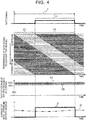
- FIG. 4 shows a control sequence according to which a given number of the battery modules 102a, 102b, ..., 102n are sequentially connected in series, to deliver electric power.
- the battery modules 102a, 102b, ..., 102n are driven one after another from the upstream side to the downstream side, with a fixed delay time.
- period E1 indicates a state (connected state) in which the first switch elements 16 of the battery modules 102a, 102b, ..., 102n are OFF, and the second switch elements 18 are ON, so that voltage is generated from the output terminals of the battery modules 102a, 102b, ..., 102n.
- period E2 indicates a state (through state) in which the first switch elements 16 of the battery modules 102a, 102b, ..., 102n are ON, and the second switch elements 18 are OFF, so that no voltage is generated from the output terminals of the battery modules 102a, 102b, ..., 102n.
- the battery modules 102a, 102b, ..., 102n are sequentially driven with the fixed delay time.
- the period T of the gate signal is set by adding the delay times of the battery modules 102a, 102b, ..., 102n together.
- the frequency of the gate signal is lower as the delay time is set to be longer.
- the frequency of the gate signal is higher as the delay time is set to be shorter.
- the delay time by which the gate signal is delayed is set as appropriate, according to the specifications required of the power supply system 100.
- the ON-time ratio D (ON-duty D) in the period T of the gate signal, namely, the ratio of time T ON for which the gate signal is at the high (H) level, to the period T, is calculated by dividing the output voltage of the power supply system 100 by the total voltage of the battery modules 102a, 102b, ..., 102n, i.e., (output voltage of the power supply system 100) / (total voltage of the battery modules 102a, 102b, ..., 102n).
- the ON-time ratio D (output voltage of the power supply system 100) / (the battery voltage of the battery module 102 ⁇ the total number of the battery modules 102).
- the ON-time ratio varies due to the dead time dt; therefore, it is preferable to correct the ON-time ratio in a feedback or feedforward manner, as generally performed by a chopper circuit.
- the output voltage of the power supply system 100 is represented by a value obtained by multiplying the battery voltage of each battery module 102 by the number of the battery modules 102 that are in the connected state.
- the output voltage of the power supply system 100 is a value that can be exactly divided by the battery voltage of one battery module 102, some battery modules 102 are switched from the connected state to the through state, at the moment when other battery modules 102 are switched from the through state to the connected state. Thus, there is no variation in the output voltage of the battery modules 102 as a whole.
- the output voltage of the power supply system 100 is a value that cannot be exactly divided by the battery voltage of each battery module 102
- the output voltage of the power supply system 100 (the overall output voltage) varies.
- the variable amplitude is the voltage of one battery module
- the variable period is obtained by dividing the period T of the gate signal by the total number of the battery modules 102.
- the output voltage HI in the form of rectangular wave is provided by the power supply system 100, as shown in FIG. 4 .
- the gate signal applied to the most upstream battery module 102a is applied with a delay of a given time, to the downstream battery module 102b, and the gate signal is further sequentially transmitted to the downstream battery modules 102 with the delay of the given time for each module, so that the battery modules 102a, 102b, ..., 102n sequentially deliver voltages, with the delay of the given time. Then, these voltages are added up, to provide the voltage of the power supply system 100. In this manner, the desired voltage can be delivered from the power supply system 100.
- the desired voltage can be easily provided by adjusting the ON-time ratio D, and the versatility of the power supply system 100 can be improved.
- the desired voltage can obtained by excluding the faulty battery module 102, using normal battery modules 102, and resetting the period T of the gate signal, ON-time ratio D, and delay time. Namely, even when a failure occurs in any of the battery modules 102a, 102b, ..., 102n, the desired voltage can be kept generated.
- FIG. 5 is a flowchart of an internal resistance measurement process of the battery module 102 according to this embodiment. Referring to FIG. 5 , the internal resistance measurement process of the battery module 102 will be described.
- step S10 an output current lout from the power supply system 100 is measured.
- the controller 104 obtains a measurement value of the output current lout, from a current sensor 32 provided in an output line of the power supply system 100.
- the module current Imod is calculated according to the relationship between the output current lout of the power supply system 100 and the ON-time ratio D (ON-duty D). Accordingly, there is no need to provide a current sensor in each battery module 102, and the manufacturing cost of the power supply system 100 can be reduced.
- step S14 the module voltage Vmod of the battery module 102 is measured.
- the controller 104 obtains a measurement value of the module voltage Vmod, from a voltage sensor 30 provided in each battery module 102 of the power supply system 100.
- the module voltage Vmod (connection voltage CCV) of each battery module 102 that is not forced to be disconnected is measured.
- step S16 a process of disconnecting a certain battery module 102 and a disconnection determining process are performed.
- the controller 104 places the battery module 102 of which the internal resistance Rmod is to be measured, in a forcedly disconnected state. More specifically, the controller 104 applies a low(L)-level control signal, to the AND element 22 of the battery module 102 as an object of forced disconnection. As a result, the battery module 102 as the object of forced disconnection is disconnected from series connection.
- the controller 104 proceeds to step S18 when the battery module 102 is disconnected, and returns to step S14 if not.
- step S18 the module voltage Vmod of the battery module 102 is measured.
- the controller 104 obtains a measurement value of the module voltage Vmod, from the voltage sensor 30 provided in each battery module 102 of the power supply system 100.
- the module voltage Vmod open-circuit voltage OCV
- a time difference between prior to disconnection and immediately after disconnection may be set to about 10 ⁇ s, for example.
- a potential difference ⁇ V is calculated. As shown in FIG. 7 , in the module voltage Vmod of the battery module 102, a potential difference ⁇ V appears between the connection voltage CCV prior to disconnection, and the open-circuit voltage OCV immediately after disconnection.
- step S22 the internal resistance Rmod of the battery module 102 is calculated.
- Eq. (4) is obtained by modifying Eq. (3) above.
- the controller 104 calculates the internal resistance Rmod of the battery module 102, according to Eq. (4).
- Rmod ⁇ V / Imod
- the internal resistance Rmod of the battery module 102 can be obtained.
- the internal resistance Rmod can also be estimated even during operation of the power supply system 100.
- the current can be reduced in steps to zero, and the potential difference ⁇ V due to the internal resistance Rmod of the battery 10 can be accurately measured.
- the internal resistance Rmod can also be estimated with high accuracy.
- the relationship between a combination of the module current Imod and the potential difference ⁇ V, and the internal resistance Rmod, may be examined in advance, and stored in a storage that can be accessed from the controller 104, so that the internal resistance Rmod can be obtained by measuring the module current Imod and the potential difference ⁇ V.
- the module voltage Vmod (connection voltage CCV) is measured in step S14 of FIG. 5
- the module voltage Vmod (open-circuit voltage OCV) is measured in step S18.
- these steps may be reversed. Namely, when the battery module 102 is brought from the forcedly disconnected state into the connected state, a potential difference ⁇ V between prior to the connection and immediately after the connection may be obtained. With this method, too, the internal resistance Rmod can be estimated.
Abstract
A power supply system includes a controller (104), and a plurality of battery modules (102). The battery modules (102) are connected in series, according to a gate drive signal from the controller (104), to provide series connection, and each of the battery modules (102) has a disconnecting device (22) configured to force the battery module to be disconnected from the series connection. The controller (104) is configured to estimate the internal resistance of the battery module disconnected from the series connection by the disconnecting device (22), from a module voltage of the battery module before the battery module is disconnected from the series connection, a module voltage immediately after the battery module is disconnected, and a module current delivered from the battery module.
Description
- The invention relates to a power supply system in which battery modules are connected in series, to supply electric power.
- A power supply system in which a plurality of battery modules is connected in series, to supply electric power (for power running) to a load, is used. When batteries included in the battery modules are secondary batteries, the batteries can be charged (regenerated) with power from the load side.
- In the power supply system as described above, it has been proposed to provide each battery module with a switching circuit that connects and disconnects the battery module to and from the load, based on a gate drive signal. In this circuit arrangement, voltage control is performed by driving the switching circuit of each battery module, with the gate drive signal applied via a delay circuit (see Japanese Unexamined Patent Application Publication No.
2018-074709 JP 2018-074709 A - Also, a method of computing the internal resistance of a secondary battery, which has a first stage and a second stage, is disclosed in Japanese Unexamined Patent Application Publication No.
2010-249770 JP 2010-249770 A - In the power supply system, it is desirable to be able to measure the internal resistance of the battery included in each of the battery modules, with high accuracy, so as to be aware of deterioration conditions, etc. of the battery. However, the manufacturing cost of the power supply system will increase if a current sensor is provided for each battery module so as to measure the internal resistance of the battery.
- A first aspect of the invention provides a power supply system. The power supply system includes a controller, and a plurality of battery modules each having a secondary battery. The battery modules are configured to be connected in series, according to a gate drive signal from the controller, to provide series connection, and each of the battery modules has a disconnecting device configured to force the battery module to be disconnected from the series connection. The controller is configured to estimate an internal resistance of the battery module disconnected from the series connection by the disconnecting device, from a module voltage of the battery module before the battery module is disconnected from the series connection, a module voltage immediately after the battery module is disconnected, and a module current delivered from the battery module.
- A second aspect of the invention provides another power supply system. The power supply system includes a controller, and a plurality of battery modules each having a secondary battery. The battery modules are configured to be connected in series, according to a gate drive signal from the controller, to provide series connection, and each of the battery modules has a disconnecting device configured to force the battery module to be disconnected from the series connection. The controller is configured to estimate an internal resistance of the battery module connected to the series connection, from a module voltage of the battery module before the battery module is connected to the series connection from a state in which the battery module is disconnected from the series connection by the disconnecting device, a module voltage immediately after the battery module is connected to the series connection, and a module current delivered from the battery module.
- In the power supply system of each of the first and second aspects, the controller may be configured to estimate the module current, from an output current delivered from the power supply system and an ON-duty set for the battery module.
- In the power supply system of the first aspect, the controller may be configured to estimate the internal resistance, from an absolute value of a difference between the module voltage before the battery module is disconnected from the series connection by the disconnecting device, and the module voltage immediately after the battery module is disconnected from the series connection, and the module current.
- In the power supply system of the second aspect, the controller may be configured to estimate the internal resistance from an absolute value of a difference between the module voltage before the battery module is connected to the series connection from the state in which the battery module is disconnected from the series connection by the disconnecting device, and the module voltage immediately after the battery module is connected to the series connection, and the module current.
- According to this invention, it is possible to measure the internal resistance of the battery included in each battery module with high accuracy, without providing a current sensor for each battery module.
- Features, advantages, and technical and industrial significance of exemplary embodiments of the invention will be described below with reference to the accompanying drawings, in which like numerals denote like elements, and wherein:
-
FIG. 1 is a view showing the configuration of a power supply system according to one embodiment of the invention; -
FIG. 2 is a time chart useful for describing control of a battery module in the embodiment of the invention; -
FIG. 3A is a view showing one example of operation of the battery module in the embodiment of the invention: -
FIG. 3B is a view showing another example of operation of the battery module in the embodiment of the invention; -
FIG. 4 is a time chart useful for describing control of the power supply system in the embodiment of the invention; -
FIG. 5 is a flowchart illustrating a process of estimating the internal resistance in the embodiment of the invention; -
FIG. 6 is a view useful for describing module current in the embodiment of the invention; and -
FIG. 7 is a view useful for describing module voltage in the embodiment of the invention. - As shown in
FIG. 1 , apower supply system 100 according to one embodiment includes a plurality of battery modules 102 (102a, 102b, ..., 102n) and acontroller 104. The battery modules 102 can be connected in series under control of thecontroller 104. The battery modules 102 included in thepower supply system 100 can supply electric power (for power running) to a load (not shown) connected to terminals T1 and T2, or can be charged (regenerated) with electric power from a power supply (not shown) connected to the terminals T1 and T2. - Each of the battery modules 102 includes a
battery 10,choke coil 12,capacitor 14,first switch element 16,second switch element 18,delay circuit 20, ANDelement 22, andNOT element 24. In this embodiment, eachbattery module - The
battery 10 includes at least one secondary cell. Thebattery 10 is composed of a plurality of lithium-ion cells, nickel-hydrogen cells, or the like, connected in series and/or in parallel, for example. Thechoke coil 12 and thecapacitor 14 constitute a smoothing circuit (low-pass filter circuit) that smooths and delivers output from thebattery 10. Since one or more secondary cells are used in thebattery 10, an RLC filter is formed by thebattery 10,choke coil 12 andcapacitor 14, for smoothing of current, so as to curb deterioration of thebattery 10 due to increase of an internal resistance loss. - The
choke coil 12 and thecapacitor 14 are not essential components, and may not be provided. In the battery module 102, the positions at which thechoke coil 12 and thebattery 10 are placed (connected) may be switched with each other. Also, thesecond switch element 18 may be placed on the opposite side of the output terminals with respect to thefirst switch element 16. Namely, the arrangement of respective elements and electric components may be changed as appropriate, provided that the voltage of the battery 10 (capacitor 14) can be applied to the output terminals, through switching operation of thefirst switch element 16 and thesecond switch element 18. - The
first switch element 16 includes a switching device for short-circuiting the output ends of thebattery 10. In this embodiment, thefirst switch element 16 is configured such that a freewheeling diode is connected in parallel with a field-effect transistor as the switching device. Thesecond switch element 18 is placed between thebattery 10 and thefirst switch element 16, and is connected in series with thebattery 10. In this embodiment, thesecond switch element 18 is configured such that a freewheeling diode is connected in parallel with a field-effect transistor as a switching device. Switching of thefirst switch element 16 and thesecond switch element 18 is controlled according to a gate signal (gate drive signal) from thecontroller 104. While the field-effect transistors are used as thefirst switch element 16 and thesecond switch element 18 in this embodiment, switching devices other than the field-effect transistors may be used. - The
delay circuit 20 serves to delay the gate signal transmitted from thecontroller 104 to each battery module 102, by a predetermine time. In thepower supply system 100, each of thebattery modules delay circuit 20, and thedelay circuits 20 of the respective battery modules 102 are connected in series. Accordingly, the gate signal received from thecontroller 104 is sequentially applied to thebattery modules - The
AND element 22 constitutes a disconnecting device that forcedly disconnects the corresponding battery module 102 from the series-connected state, according to a forced disconnection signal. TheAND element 22 is controlled in response to the forced disconnection signal from thecontroller 104. TheAND element 22 has one input terminal that receives a control signal from thecontroller 104, and the other input terminal that receives the gate drive signal from thedelay circuit 20. An output signal from the ANDelement 22 is transmitted to a gate terminal of thesecond switch element 18. The output signal from the ANDelement 22 is also transmitted to a gate terminal of thefirst switch element 16 via theNOT element 24. - Under normal control, the
controller 104 sends a high(H)-level control signal to the ANDelement 22. Accordingly, the gate drive signal is transmitted as it is to the gate terminal of thesecond switch element 18, and an inversion signal of the gate drive signal is transmitted to the gate terminal of thefirst switch element 16. As a result, when the gate drive signal is at a high (H) level, thefirst switch element 16 is placed in the OFF state, and thesecond switch element 18 is placed in the ON state. When the gate drive signal is at a low (L) level, thefirst switch element 16 is placed in the ON state, and thesecond switch element 18 is placed in the OFF state. Namely, the battery module 102 to which the high(H)-level gate drive signal is applied is connected in series with the other battery modules 102, and the battery module 102 to which the low(L)-level gate drive signal is applied is disconnected from the other battery modules 102, and placed in a through state. - At the time of forced disconnection, the
controller 104 sends a low(L)-level control signal to the ANDelement 22. As a result, a low(L)-level signal is generated from the ANDelement 22, and a high(H)-level signal is received by the gate terminal of thefirst switch element 16 via theNOT element 24, while the low(L)-level signal is received by the gate terminal of thesecond switch element 18. Accordingly, thefirst switch element 16 is placed in the ON state all the time, and thesecond switch element 18 is placed in the OFF state all the time, so that the battery module 102 is placed in a state (path-through state) in which it is forced to be disconnected from series connection, irrespective of the level of the gate drive signal. - The forced disconnection control as described above may be used as control for reducing imbalance of the SOC among the battery modules 102 in the
power supply system 100, and may be used for disconnection of a battery module when it fails. Namely, when thepower supply system 100 is in a state of discharge, the SOC of the battery modules 102 involved in output of thepower supply system 100 is reduced. However, if any of the battery modules 102 is brought into a forced disconnected state, the SOC of the battery module 102 can be kept at the same level. Also, when thepower supply system 100 is in a state of charge, the SOC of the battery modules 102 involved in charging of thepower supply system 100 is increased. However, if any of the battery modules 102 is brought into the forced disconnected state, the SOC of the battery module 102 can be kept at the same level. - While the
delay circuit 20 is placed in the preceding stage of the ANDelement 22 in this embodiment, it may be placed in the trailing stage of the ANDelement 22. Namely, any arrangement may be employed provided that the gate signal, which is delayed by a predetermined time in each battery module 102, is sequentially transmitted to thedelay circuits 20 of the downstream battery modules 102. - Referring to
FIG. 2 , control of thepower supply system 100 will be described. Under normal control, the high(H)-level control signal is transmitted from thecontroller 104 to the ANDelement 22 of each of thebattery modules first switch element 16 receives an inversion signal of the output signal from thedelay circuit 20 via theNOT element 24, and the gate terminal of thesecond switch element 18 receives the output signal from thedelay circuit 20 as it is. - The time chart of
FIG. 2 is concerned with operation of thebattery module 102a.FIG. 2 shows pulse waveform of the gate signal D1 that drives thebattery module 102a, rectangular wave D2 indicating a switching state of thefirst switch element 16, rectangular wave D3 indicating a switching state of thesecond switch element 18, and waveform D4 of output voltage Vmod of thebattery module 102a. - In the initial state of the
battery module 102a, namely, in a condition where no gate signal is generated, thefirst switch element 16 is in the ON state, and thesecond switch element 18 is in the OFF state. Then, when a gate signal is transmitted from thecontroller 104 to thebattery module 102a, switching control in the form of PWM control is performed on thebattery module 102a. Under the switching control, thefirst switch element 16 and thesecond switch element 18 are alternately placed in the ON state and the OFF state. - As shown in
FIG. 2 , when the gate signal D1 is generated from thecontroller 104, thefirst switch element 16 andsecond switch element 18 of thebattery module 102a are driven, according to the gate signal D1. Thefirst switch element 16 is switched from the ON state to the OFF state, in response to a fall of the signal from theNOT element 24 responsive to a rise of the gate signal D1. Also, thefirst switch element 16 is switched from the OFF state to the ON state, with a slight time delay (dead time dt) from a fall of the gate signal D1. - On the other hand, the
second switch element 18 is switched from the OFF state to the ON state, with a slight time delay (dead time dt) from a rise of the gate signal D1. Also, thesecond switch element 18 is switched from the ON state to the OFF state, at the same time as a fall of the gate signal D1. Thus, thefirst switch element 16 and thesecond switch element 18 are controlled so as to be alternately switched between the ON state and the OFF state. - The
first switch element 16 operates with a slight time delay (dead time dt) upon a fall of the gate signal D1, and thesecond switch element 18 operates with a slight time delay (dead time dt) upon a rise of the gate signal D1, so that thefirst switch element 16 and thesecond switch element 18 are prevented from operating at the same time. Namely, thefirst switch element 16 and thesecond switch element 18 are prevented from being turned ON at the same time and short-circuited. The dead time dt for which the operation is delayed is set to 100 ns, for example, but may be set as appropriate. During the dead time dt, current flows backward through a diode, so that the switch element is brought into the same condition as that in which the switching device disposed in parallel with the diode is turned ON. - Through the above control, when the gate signal D1 applied to the
battery module 102a is OFF (namely, when thefirst switch element 16 is ON, and thesecond switch element 18 is OFF), thecapacitor 14 is disconnected from the output terminals of thebattery module 102a. Accordingly, no voltage is applied from thebattery module 102a to the output terminals. In this condition, thebattery module 102a is placed in a through state in which the battery 10 (capacitor 14) of thebattery module 102a is bypassed, as shown inFIG. 3A . - When the gate signal D1 is ON (namely, when the
first switch element 16 is OFF, and thesecond switch element 18 is ON), thecapacitor 14 is connected to the output terminals of thebattery module 102a. Accordingly, a voltage is applied from thebattery module 102a to the output terminals. In this conditions, the voltage Vmod is applied to the output terminals via thecapacitor 14 in thebattery module 102a, as shown inFIG. 3B . - Referring back to
FIG. 1 , control of thepower supply system 100 by means of thecontroller 104 will be described. Thecontroller 104 controls the whole set of the battery modules 102. Namely, thecontroller 104 controls a plurality ofbattery modules power supply system 100. - The
controller 104 includes a gate circuit that generates a gate signal in the form of rectangular wave, to each battery module 102. The gate signal is sequentially transmitted to the battery modules 102 of the downstream stages, via thedelay circuit 20 included in thebattery module 102a,delay circuit 20 included in thebattery module 102b, and so forth. Namely, the gate signal is sequentially transmitted from the most upstream side of the battery modules 102 connected in series in thepower supply system 100, to the downstream side, while being delayed by a predetermined delay time in each battery module. - Under normal control, the high(H)-level control signal is applied from the
controller 104 to the ANDelement 22; therefore, the gate signal delivered from thedelay circuit 20 of each battery module 102 is applied as it is to the gate terminal of thesecond switch element 18, and a signal obtained by inverting the gate signal is applied to the gate terminal of thefirst switch element 16. Accordingly, when the gate signal is at the high (H) level, thefirst switch element 16 is placed in the OFF state, and thesecond switch element 18 is placed in the ON state. When the gate signal is at the low (L) level, thefirst switch element 16 is placed in the ON state, and thesecond switch element 18 is placed in the OFF state. - Namely, the battery module 102 to which the high(H)-level gate signal is applied is placed in a state in which it is connected in series with the other battery modules 102, and the battery module 102 to which the low(L)-level gate signal is applied is placed in a through state in which it is disconnected from the other battery modules 102.
-
FIG. 4 shows a control sequence according to which a given number of thebattery modules FIG. 4 , in response to the gate signal, thebattery modules FIG. 4 , period E1 indicates a state (connected state) in which thefirst switch elements 16 of thebattery modules second switch elements 18 are ON, so that voltage is generated from the output terminals of thebattery modules first switch elements 16 of thebattery modules second switch elements 18 are OFF, so that no voltage is generated from the output terminals of thebattery modules battery modules - Referring to
FIG. 4 , the manner of setting the gate signal and the delay time of the gate signal will be described. The period T of the gate signal is set by adding the delay times of thebattery modules power supply system 100. - The ON-time ratio D (ON-duty D) in the period T of the gate signal, namely, the ratio of time TON for which the gate signal is at the high (H) level, to the period T, is calculated by dividing the output voltage of the
power supply system 100 by the total voltage of thebattery modules battery modules - As described above, the output voltage of the
power supply system 100 is represented by a value obtained by multiplying the battery voltage of each battery module 102 by the number of the battery modules 102 that are in the connected state. When the output voltage of thepower supply system 100 is a value that can be exactly divided by the battery voltage of one battery module 102, some battery modules 102 are switched from the connected state to the through state, at the moment when other battery modules 102 are switched from the through state to the connected state. Thus, there is no variation in the output voltage of the battery modules 102 as a whole. - However, when the output voltage of the
power supply system 100 is a value that cannot be exactly divided by the battery voltage of each battery module 102, the output voltage of the power supply system 100 (the overall output voltage) varies. In this case, the variable amplitude is the voltage of one battery module, and the variable period is obtained by dividing the period T of the gate signal by the total number of the battery modules 102. When several dozens of battery modules 102 are connected in series, the parasitic inductance of thepower supply system 100 as a whole becomes a large value, and the voltage variation is filtered out, so that a stable output voltage of thepower supply system 100 can be eventually obtained. - Next, a specific example will be described. In
FIG. 4 , it is assumed that a desired output voltage of thepower supply system 100 is 400 V, the battery voltage of each battery module 102 is 15V, the total number of thebattery modules power supply system 100 cannot be exactly divided by the battery voltage (15V) of the battery module 102. - The period T of the gate signal is calculated by multiplying the delay time by the total number of the battery modules 102; thus, the period T is 8 µs (= 200 ns × 40), based on the above numerical values. Accordingly, the gate signal is in the form of rectangular wave having a frequency of 125 kHz. Also, the ON-time ratio D of the gate signal is calculated by dividing the output voltage of the
power supply system 100 by (battery voltage of the battery module 102 × the total number of the battery modules 102); thus the ON-time ratio D becomes substantially equal to 0.67, namely, 400 V / (15 V × 40) ≈ 0.67. - When the
battery modules power supply system 100, as shown inFIG. 4 . The output voltage HI varies between 390 V and 405 V. Namely, the output voltage HI varies at intervals of a period T calculated by dividing the period T of the gate signal by the total number of the battery modules, namely, at intervals of 200 ns (= 8 µs / 40) (corresponding to 5 MHz). This variation is filtered out by the parasitic inductance caused by wirings of thebattery modules power supply system 100 as a whole delivers an output voltage H2 of about 400 V. - In this connection, electric current flows to the
capacitor 14 of each battery module 102 when the battery module 102 is in the connected state, and the capacitor current waveform J1 becomes rectangular wave, as shown inFIG. 4 . Also, since thebattery 10 and thecapacitor 14 form the RLC filter, current J2 that has been filtered and smoothed flows in thepower supply system 100. Thus, the current waveform is uniform over all of thebattery modules battery modules - As described above, when the
power supply system 100 is controlled, the gate signal applied to the mostupstream battery module 102a is applied with a delay of a given time, to thedownstream battery module 102b, and the gate signal is further sequentially transmitted to the downstream battery modules 102 with the delay of the given time for each module, so that thebattery modules power supply system 100. In this manner, the desired voltage can be delivered from thepower supply system 100. - In the
power supply system 100, no booster circuit is required, and the circuit configuration can be simplified, so that the size and the cost can be reduced. Also, a balance circuit, or the like, which causes a power loss is not required, and the efficiency of thepower supply system 100 can be enhanced. Further, voltage is substantially equally or evenly delivered from thebattery modules power supply system 100 can be reduced. - Also, the desired voltage can be easily provided by adjusting the ON-time ratio D, and the versatility of the
power supply system 100 can be improved. In particular, even when a failure occurs in one of thebattery modules battery modules - Further, the frequency of the gate signal becomes lower as the delay time by which the gate signal is delayed is set to be longer; as a result, the switching frequencies of the
first switch element 16 and thesecond switch element 18 are lowered, and the switching loss can be reduced, so that the power conversion efficiency can be improved. Conversely, the frequency of the gate signal becomes higher as the delay time by which the gate signal is delayed is set to be shorter; as a result, the frequency of voltage variation becomes higher, which makes filtering easy, and a stable voltage can be obtained. Also, the use of the RLC filter makes it easy to smooth or level current variations. Thus, it is possible to provide thepower supply system 100 according to the required specifications and performance, by adjusting the delay time by which the gate signal is delayed. -
FIG. 5 is a flowchart of an internal resistance measurement process of the battery module 102 according to this embodiment. Referring toFIG. 5 , the internal resistance measurement process of the battery module 102 will be described. - In step S10, an output current lout from the
power supply system 100 is measured. Thecontroller 104 obtains a measurement value of the output current lout, from acurrent sensor 32 provided in an output line of thepower supply system 100. - In step S12, the module current Imod of the battery modules 102 is calculated. As shown in
FIG. 6 , the module current Imod in each battery module 102 is equal to a value of current delivered during the ON time of the ON-time ratio D (ON-duty D) so that the output current lout is generated by the battery modules 102 connected in series; thus, the module current Imod is obtained by multiplying the output current lout by the ON-time ratio D (ON-duty D), as indicated by Eq. (1) below.
- In the
power supply system 100, the module current Imod is calculated according to the relationship between the output current lout of thepower supply system 100 and the ON-time ratio D (ON-duty D). Accordingly, there is no need to provide a current sensor in each battery module 102, and the manufacturing cost of thepower supply system 100 can be reduced. - In step S14, the module voltage Vmod of the battery module 102 is measured. The
controller 104 obtains a measurement value of the module voltage Vmod, from avoltage sensor 30 provided in each battery module 102 of thepower supply system 100. Here, the module voltage Vmod (connection voltage CCV) of each battery module 102 that is not forced to be disconnected is measured. - In step S16, a process of disconnecting a certain battery module 102 and a disconnection determining process are performed. The
controller 104 places the battery module 102 of which the internal resistance Rmod is to be measured, in a forcedly disconnected state. More specifically, thecontroller 104 applies a low(L)-level control signal, to the ANDelement 22 of the battery module 102 as an object of forced disconnection. As a result, the battery module 102 as the object of forced disconnection is disconnected from series connection. Thecontroller 104 proceeds to step S18 when the battery module 102 is disconnected, and returns to step S14 if not. - In step S18, the module voltage Vmod of the battery module 102 is measured. The
controller 104 obtains a measurement value of the module voltage Vmod, from thevoltage sensor 30 provided in each battery module 102 of thepower supply system 100. Here, the module voltage Vmod (open-circuit voltage OCV) of each battery module 102 immediately after it was forced to be disconnected is measured. A time difference between prior to disconnection and immediately after disconnection may be set to about 10 µs, for example. - In step S20, a potential difference ΔV is calculated. As shown in
FIG. 7 , in the module voltage Vmod of the battery module 102, a potential difference ΔV appears between the connection voltage CCV prior to disconnection, and the open-circuit voltage OCV immediately after disconnection. Thecontroller 104 calculates an absolute value of a difference between the module voltage Vmod (open-circuit voltage OCV) measured in step S18 and the module voltage Vmod (connection voltage CCV) measured in step S14, as the potential difference ΔV, using Eq. (2) as follows.
- In step S22, the internal resistance Rmod of the battery module 102 is calculated. The potential difference ΔV represents a voltage drop caused by the internal resistance Rmod of the
battery 10 included in the battery module 102. Accordingly, the potential difference ΔV is expressed by Eq. (3) as follows.
- Eq. (4) below is obtained by modifying Eq. (3) above. The
controller 104 calculates the internal resistance Rmod of the battery module 102, according to Eq. (4).
- In the manner as described above, the internal resistance Rmod of the battery module 102 can be obtained. The internal resistance Rmod can also be estimated even during operation of the
power supply system 100. In this embodiment, the current can be reduced in steps to zero, and the potential difference ΔV due to the internal resistance Rmod of thebattery 10 can be accurately measured. Thus, the internal resistance Rmod can also be estimated with high accuracy. - Further, according to the
power supply system 100 of this embodiment, it is possible to obtain the internal resistance Rmod of each of the battery modules 102, without providing a current sensor in each battery module 102. - The relationship between a combination of the module current Imod and the potential difference ΔV, and the internal resistance Rmod, may be examined in advance, and stored in a storage that can be accessed from the
controller 104, so that the internal resistance Rmod can be obtained by measuring the module current Imod and the potential difference ΔV. - In this embodiment, the module voltage Vmod (connection voltage CCV) is measured in step S14 of
FIG. 5 , and the module voltage Vmod (open-circuit voltage OCV) is measured in step S18. However, these steps may be reversed. Namely, when the battery module 102 is brought from the forcedly disconnected state into the connected state, a potential difference ΔV between prior to the connection and immediately after the connection may be obtained. With this method, too, the internal resistance Rmod can be estimated.
Claims (5)
- A power supply system (100) comprising:a controller (104); anda plurality of battery modules (102) each having a secondary battery (10), the battery modules (102) being configured to be connected in series, according to a gate drive signal from the controller (104), to provide series connection, each of the battery modules (102) having a disconnecting device (22) configured to force the battery module to be disconnected from the series connection,wherein the controller (104) is configured to estimate an internal resistance of the battery module disconnected from the series connection by the disconnecting device (22), from a module voltage of the battery module before the battery module is disconnected from the series connection, a module voltage immediately after the battery module is disconnected, and a module current delivered from the battery module.
- A power supply system (100) comprising:a controller (104); anda plurality of battery modules (102) each having a secondary battery (10), the battery modules (102) being configured to be connected in series, according to a gate drive signal from the controller (104), to provide series connection, each of the battery modules (102) having a disconnecting device (22) configured to force the battery module to be disconnected from the series connection,wherein the controller (104) is configured to estimate an internal resistance of the battery module connected to the series connection, from a module voltage of the battery module before the battery module is connected to the series connection from a state in which the battery module is disconnected from the series connection by the disconnecting device (22), a module voltage immediately after the battery module is connected to the series connection, and a module current delivered from the battery module.
- The power supply system (100) according to claim 1 or 2, wherein the controller (104) is configured to estimate the module current, from an output current delivered from the power supply system (100) and an ON-duty set for the battery module.
- The power supply system (100) according to claim 1, wherein the controller (104) is configured to estimate the internal resistance, from an absolute value of a difference between the module voltage before the battery module is disconnected from the series connection by the disconnecting device (22), and the module voltage immediately after the battery module is disconnected from the series connection, and the module current.
- The power supply system (100) according to claim 2, wherein the controller (104) is configured to estimate the internal resistance from an absolute value of a difference between the module voltage before the battery module is connected to the series connection from the state in which the battery module is disconnected from the series connection by the disconnecting device (22), and the module voltage immediately after the battery module is connected to the series connection, and the module current.
Applications Claiming Priority (1)
| Application Number | Priority Date | Filing Date | Title |
|---|---|---|---|
| JP2018204647A JP7077204B2 (en) | 2018-10-31 | 2018-10-31 | Power supply |
Publications (1)
| Publication Number | Publication Date |
|---|---|
| EP3648291A1 true EP3648291A1 (en) | 2020-05-06 |
Family
ID=68342550
Family Applications (1)
| Application Number | Title | Priority Date | Filing Date |
|---|---|---|---|
| EP19204682.9A Pending EP3648291A1 (en) | 2018-10-31 | 2019-10-22 | Power supply system |
Country Status (5)
| Country | Link |
|---|---|
| US (1) | US11302970B2 (en) |
| EP (1) | EP3648291A1 (en) |
| JP (1) | JP7077204B2 (en) |
| KR (1) | KR102271514B1 (en) |
| CN (1) | CN111130163B (en) |
Families Citing this family (5)
| Publication number | Priority date | Publication date | Assignee | Title |
|---|---|---|---|---|
| JP6960898B2 (en) * | 2018-10-31 | 2021-11-05 | 株式会社豊田中央研究所 | Power supply |
| JP6898904B2 (en) | 2018-10-31 | 2021-07-07 | 株式会社豊田中央研究所 | Power supply |
| JP6960897B2 (en) | 2018-10-31 | 2021-11-05 | 株式会社豊田中央研究所 | Power supply |
| EP3916948A1 (en) * | 2020-05-28 | 2021-12-01 | STABL Energy GmbH | Modular energy storage system |
| CN113998123B (en) * | 2021-10-09 | 2023-06-02 | 广东汇天航空航天科技有限公司 | Power system, flyable device and power control method |
Citations (5)
| Publication number | Priority date | Publication date | Assignee | Title |
|---|---|---|---|---|
| JP2010249770A (en) | 2009-04-20 | 2010-11-04 | Nissan Motor Co Ltd | Internal resistance operation method of secondary battery |
| US20120013304A1 (en) * | 2009-03-27 | 2012-01-19 | The Japan Research Institute, Limited | Battery control apparatus, vehicle, and battery control method |
| WO2018062394A1 (en) * | 2016-09-29 | 2018-04-05 | 株式会社Gsユアサ | Power storage element soc estimation device, power storage device, and power storage element soc estimation method |
| JP2018074709A (en) | 2016-10-27 | 2018-05-10 | 株式会社豊田中央研究所 | Power unit and metho for controlling power unit |
| WO2018179774A1 (en) * | 2017-03-31 | 2018-10-04 | 株式会社豊田中央研究所 | Power supply device |
Family Cites Families (27)
| Publication number | Priority date | Publication date | Assignee | Title |
|---|---|---|---|---|
| JPH05188123A (en) | 1992-01-10 | 1993-07-30 | Asia Electron Inc | Battery measuring apparatus |
| JP2002354703A (en) * | 2001-05-25 | 2002-12-06 | Toyota Motor Corp | Secondary battery control device for vehicles |
| JP4228760B2 (en) * | 2002-07-12 | 2009-02-25 | トヨタ自動車株式会社 | Battery charge state estimation device |
| JP4665569B2 (en) * | 2004-11-30 | 2011-04-06 | トヨタ自動車株式会社 | VOLTAGE CONVERTER AND COMPUTER-READABLE RECORDING MEDIUM RECORDING PROGRAM FOR CAUSING COMPUTER TO EXECUTE VOLTAGE CONVERSION IN VOLTAGE CONVERTER |
| JP4622645B2 (en) * | 2005-04-15 | 2011-02-02 | トヨタ自動車株式会社 | Battery device, internal combustion engine device including the same, and vehicle |
| JP2008011657A (en) * | 2006-06-29 | 2008-01-17 | Sanyo Electric Co Ltd | Power supply unit |
| WO2010042517A1 (en) * | 2008-10-07 | 2010-04-15 | Boston-Power, Inc. | Li-ion battery array for vehicle and other large capacity applications |
| JP5638779B2 (en) * | 2009-08-24 | 2014-12-10 | 三洋電機株式会社 | Secondary battery characteristic detection method and secondary battery device |
| CA2782502C (en) * | 2009-12-22 | 2017-06-13 | Abb Research Ltd. | Battery energy storage system with short circuit protection, and method |
| TWI404963B (en) | 2010-02-10 | 2013-08-11 | Chung Shan Inst Of Science | Method for detecting battery module status |
| JPWO2012043590A1 (en) * | 2010-09-30 | 2014-02-24 | 三洋電機株式会社 | Power supply |
| JP2012182882A (en) * | 2011-02-28 | 2012-09-20 | Toshiba Corp | Secondary battery device |
| WO2013046714A1 (en) * | 2011-09-30 | 2013-04-04 | パナソニック株式会社 | Internal resistance detecting circuit and battery power supply apparatus |
| JP5892024B2 (en) * | 2012-10-01 | 2016-03-23 | 株式会社豊田自動織機 | Power supply device and battery module switching method |
| DE102012222746A1 (en) * | 2012-12-11 | 2014-06-12 | Robert Bosch Gmbh | Battery module balancing and battery management system |
| JP2014176152A (en) * | 2013-03-07 | 2014-09-22 | Tdk Corp | Power storage system |
| RU131876U1 (en) * | 2013-03-26 | 2013-08-27 | Руслан Константинович Борисов | DEVICE FOR MEASUREMENTS OF INTERNAL RESISTANCE OF STATIONARY BATTERY BATTERIES |
| US10788539B2 (en) * | 2013-04-26 | 2020-09-29 | Hitachi Automotive Systems, Ltd. | Battery monitoring device and battery system using same |
| EP3014726B1 (en) * | 2013-06-26 | 2017-07-19 | TWS (Macau Commercial Offshore) Limited | Energy storage system |
| US9726731B2 (en) * | 2013-12-31 | 2017-08-08 | Chervon (Hk) Limited | Battery pack, method for detecting battery pack, charging assembly and electric tool |
| KR20150081731A (en) * | 2014-01-06 | 2015-07-15 | 삼성에스디아이 주식회사 | Battery pack, energy storage system including the battery pack, and method of operating the battery pack |
| JP6312508B2 (en) * | 2014-04-11 | 2018-04-18 | 日立オートモティブシステムズ株式会社 | Battery monitoring device, battery system, and electric vehicle drive device |
| JP6164503B2 (en) * | 2015-06-25 | 2017-07-19 | トヨタ自動車株式会社 | Secondary battery internal resistance estimation method and output control method |
| CN205157652U (en) * | 2015-11-23 | 2016-04-13 | 上海电力学院 | Direct current undercurrent secondary discharge holds internal resistance of cell on -line measuring device |
| CN108008312A (en) * | 2017-11-27 | 2018-05-08 | 广州市扬新技术研究有限责任公司 | Storage battery group state on-line measurement circuit and method |
| CN108199445A (en) * | 2018-02-05 | 2018-06-22 | 江门市敏华电器有限公司 | The active equalization circuit and method of a kind of series-connected batteries |
| KR102374744B1 (en) * | 2018-10-16 | 2022-03-14 | 주식회사 엘지에너지솔루션 | Apparatus and method for balancing of battery module |
-
2018
- 2018-10-31 JP JP2018204647A patent/JP7077204B2/en active Active
-
2019
- 2019-10-18 US US16/657,969 patent/US11302970B2/en active Active
- 2019-10-22 KR KR1020190131063A patent/KR102271514B1/en active IP Right Grant
- 2019-10-22 CN CN201911003070.1A patent/CN111130163B/en active Active
- 2019-10-22 EP EP19204682.9A patent/EP3648291A1/en active Pending
Patent Citations (6)
| Publication number | Priority date | Publication date | Assignee | Title |
|---|---|---|---|---|
| US20120013304A1 (en) * | 2009-03-27 | 2012-01-19 | The Japan Research Institute, Limited | Battery control apparatus, vehicle, and battery control method |
| JP2010249770A (en) | 2009-04-20 | 2010-11-04 | Nissan Motor Co Ltd | Internal resistance operation method of secondary battery |
| WO2018062394A1 (en) * | 2016-09-29 | 2018-04-05 | 株式会社Gsユアサ | Power storage element soc estimation device, power storage device, and power storage element soc estimation method |
| EP3521846A1 (en) * | 2016-09-29 | 2019-08-07 | GS Yuasa International Ltd. | Power storage element soc estimation device, power storage device, and power storage element soc estimation method |
| JP2018074709A (en) | 2016-10-27 | 2018-05-10 | 株式会社豊田中央研究所 | Power unit and metho for controlling power unit |
| WO2018179774A1 (en) * | 2017-03-31 | 2018-10-04 | 株式会社豊田中央研究所 | Power supply device |
Also Published As
| Publication number | Publication date |
|---|---|
| US20200136196A1 (en) | 2020-04-30 |
| KR20200049554A (en) | 2020-05-08 |
| US11302970B2 (en) | 2022-04-12 |
| CN111130163B (en) | 2023-07-28 |
| KR102271514B1 (en) | 2021-07-02 |
| CN111130163A (en) | 2020-05-08 |
| JP2020072546A (en) | 2020-05-07 |
| JP7077204B2 (en) | 2022-05-30 |
Similar Documents
| Publication | Publication Date | Title |
|---|---|---|
| EP3648291A1 (en) | Power supply system | |
| EP3588733B1 (en) | Power supply device | |
| EP2592714B1 (en) | Apparatus and method for battery equalization | |
| US11196271B2 (en) | Full-charge-capacity estimating device for power supply device | |
| US11635469B2 (en) | Power supply device | |
| EP3648289B1 (en) | Power supply device | |
| CN111130162A (en) | Power supply apparatus | |
| JP6922337B2 (en) | Power supply and SOC estimation method in it | |
| JP7318227B2 (en) | power supply |
Legal Events
| Date | Code | Title | Description |
|---|---|---|---|
| PUAI | Public reference made under article 153(3) epc to a published international application that has entered the european phase |
Free format text: ORIGINAL CODE: 0009012 |
|
| STAA | Information on the status of an ep patent application or granted ep patent |
Free format text: STATUS: REQUEST FOR EXAMINATION WAS MADE |
|
| 17P | Request for examination filed |
Effective date: 20191022 |
|
| AK | Designated contracting states |
Kind code of ref document: A1 Designated state(s): AL AT BE BG CH CY CZ DE DK EE ES FI FR GB GR HR HU IE IS IT LI LT LU LV MC MK MT NL NO PL PT RO RS SE SI SK SM TR |
|
| AX | Request for extension of the european patent |
Extension state: BA ME |
|
| STAA | Information on the status of an ep patent application or granted ep patent |
Free format text: STATUS: EXAMINATION IS IN PROGRESS |
|
| 17Q | First examination report despatched |
Effective date: 20221206 |