EP3647932B1 - Dispositif de stockage de traitement de données de flux, système le comprenant et son procédé de fonctionnement - Google Patents
Dispositif de stockage de traitement de données de flux, système le comprenant et son procédé de fonctionnement Download PDFInfo
- Publication number
- EP3647932B1 EP3647932B1 EP19205624.0A EP19205624A EP3647932B1 EP 3647932 B1 EP3647932 B1 EP 3647932B1 EP 19205624 A EP19205624 A EP 19205624A EP 3647932 B1 EP3647932 B1 EP 3647932B1
- Authority
- EP
- European Patent Office
- Prior art keywords
- streaming
- buffer
- data
- host
- stream data
- Prior art date
- Legal status (The legal status is an assumption and is not a legal conclusion. Google has not performed a legal analysis and makes no representation as to the accuracy of the status listed.)
- Active
Links
- 238000000034 method Methods 0.000 title claims description 27
- 238000012545 processing Methods 0.000 title description 35
- 239000000872 buffer Substances 0.000 claims description 216
- 230000015654 memory Effects 0.000 claims description 165
- 238000012546 transfer Methods 0.000 claims description 29
- 230000002093 peripheral effect Effects 0.000 claims description 22
- 239000007787 solid Substances 0.000 claims description 11
- 238000013507 mapping Methods 0.000 claims description 4
- 230000004044 response Effects 0.000 description 30
- 238000010586 diagram Methods 0.000 description 29
- 230000008569 process Effects 0.000 description 16
- 230000006870 function Effects 0.000 description 11
- 238000004891 communication Methods 0.000 description 7
- 230000003936 working memory Effects 0.000 description 7
- 239000004744 fabric Substances 0.000 description 6
- 238000010025 steaming Methods 0.000 description 6
- 238000005516 engineering process Methods 0.000 description 4
- 238000012005 ligant binding assay Methods 0.000 description 4
- 238000013519 translation Methods 0.000 description 4
- 230000005540 biological transmission Effects 0.000 description 3
- 230000008859 change Effects 0.000 description 2
- 238000001514 detection method Methods 0.000 description 2
- 230000003139 buffering effect Effects 0.000 description 1
- 239000003795 chemical substances by application Substances 0.000 description 1
- 230000003247 decreasing effect Effects 0.000 description 1
- 230000001419 dependent effect Effects 0.000 description 1
- 230000000694 effects Effects 0.000 description 1
- 230000010365 information processing Effects 0.000 description 1
- 238000012986 modification Methods 0.000 description 1
- 230000004048 modification Effects 0.000 description 1
- 230000003287 optical effect Effects 0.000 description 1
- 230000002441 reversible effect Effects 0.000 description 1
- 239000004065 semiconductor Substances 0.000 description 1
- 230000003068 static effect Effects 0.000 description 1
- 239000000758 substrate Substances 0.000 description 1
- 230000001360 synchronised effect Effects 0.000 description 1
Images


Classifications
-
- G—PHYSICS
- G06—COMPUTING; CALCULATING OR COUNTING
- G06F—ELECTRIC DIGITAL DATA PROCESSING
- G06F3/00—Input arrangements for transferring data to be processed into a form capable of being handled by the computer; Output arrangements for transferring data from processing unit to output unit, e.g. interface arrangements
- G06F3/06—Digital input from, or digital output to, record carriers, e.g. RAID, emulated record carriers or networked record carriers
- G06F3/0601—Interfaces specially adapted for storage systems
- G06F3/0628—Interfaces specially adapted for storage systems making use of a particular technique
- G06F3/0629—Configuration or reconfiguration of storage systems
- G06F3/0632—Configuration or reconfiguration of storage systems by initialisation or re-initialisation of storage systems
-
- G—PHYSICS
- G06—COMPUTING; CALCULATING OR COUNTING
- G06F—ELECTRIC DIGITAL DATA PROCESSING
- G06F3/00—Input arrangements for transferring data to be processed into a form capable of being handled by the computer; Output arrangements for transferring data from processing unit to output unit, e.g. interface arrangements
- G06F3/06—Digital input from, or digital output to, record carriers, e.g. RAID, emulated record carriers or networked record carriers
- G06F3/0601—Interfaces specially adapted for storage systems
- G06F3/0668—Interfaces specially adapted for storage systems adopting a particular infrastructure
- G06F3/0671—In-line storage system
- G06F3/0673—Single storage device
- G06F3/0679—Non-volatile semiconductor memory device, e.g. flash memory, one time programmable memory [OTP]
-
- G—PHYSICS
- G06—COMPUTING; CALCULATING OR COUNTING
- G06F—ELECTRIC DIGITAL DATA PROCESSING
- G06F12/00—Accessing, addressing or allocating within memory systems or architectures
- G06F12/02—Addressing or allocation; Relocation
- G06F12/0223—User address space allocation, e.g. contiguous or non contiguous base addressing
- G06F12/023—Free address space management
- G06F12/0238—Memory management in non-volatile memory, e.g. resistive RAM or ferroelectric memory
- G06F12/0246—Memory management in non-volatile memory, e.g. resistive RAM or ferroelectric memory in block erasable memory, e.g. flash memory
-
- G—PHYSICS
- G06—COMPUTING; CALCULATING OR COUNTING
- G06F—ELECTRIC DIGITAL DATA PROCESSING
- G06F12/00—Accessing, addressing or allocating within memory systems or architectures
- G06F12/02—Addressing or allocation; Relocation
- G06F12/08—Addressing or allocation; Relocation in hierarchically structured memory systems, e.g. virtual memory systems
- G06F12/0802—Addressing of a memory level in which the access to the desired data or data block requires associative addressing means, e.g. caches
- G06F12/0862—Addressing of a memory level in which the access to the desired data or data block requires associative addressing means, e.g. caches with prefetch
-
- G—PHYSICS
- G06—COMPUTING; CALCULATING OR COUNTING
- G06F—ELECTRIC DIGITAL DATA PROCESSING
- G06F13/00—Interconnection of, or transfer of information or other signals between, memories, input/output devices or central processing units
- G06F13/38—Information transfer, e.g. on bus
- G06F13/42—Bus transfer protocol, e.g. handshake; Synchronisation
- G06F13/4204—Bus transfer protocol, e.g. handshake; Synchronisation on a parallel bus
- G06F13/4221—Bus transfer protocol, e.g. handshake; Synchronisation on a parallel bus being an input/output bus, e.g. ISA bus, EISA bus, PCI bus, SCSI bus
-
- G—PHYSICS
- G06—COMPUTING; CALCULATING OR COUNTING
- G06F—ELECTRIC DIGITAL DATA PROCESSING
- G06F3/00—Input arrangements for transferring data to be processed into a form capable of being handled by the computer; Output arrangements for transferring data from processing unit to output unit, e.g. interface arrangements
- G06F3/06—Digital input from, or digital output to, record carriers, e.g. RAID, emulated record carriers or networked record carriers
- G06F3/0601—Interfaces specially adapted for storage systems
- G06F3/0602—Interfaces specially adapted for storage systems specifically adapted to achieve a particular effect
- G06F3/061—Improving I/O performance
-
- G—PHYSICS
- G06—COMPUTING; CALCULATING OR COUNTING
- G06F—ELECTRIC DIGITAL DATA PROCESSING
- G06F3/00—Input arrangements for transferring data to be processed into a form capable of being handled by the computer; Output arrangements for transferring data from processing unit to output unit, e.g. interface arrangements
- G06F3/06—Digital input from, or digital output to, record carriers, e.g. RAID, emulated record carriers or networked record carriers
- G06F3/0601—Interfaces specially adapted for storage systems
- G06F3/0628—Interfaces specially adapted for storage systems making use of a particular technique
- G06F3/0629—Configuration or reconfiguration of storage systems
-
- G—PHYSICS
- G06—COMPUTING; CALCULATING OR COUNTING
- G06F—ELECTRIC DIGITAL DATA PROCESSING
- G06F3/00—Input arrangements for transferring data to be processed into a form capable of being handled by the computer; Output arrangements for transferring data from processing unit to output unit, e.g. interface arrangements
- G06F3/06—Digital input from, or digital output to, record carriers, e.g. RAID, emulated record carriers or networked record carriers
- G06F3/0601—Interfaces specially adapted for storage systems
- G06F3/0628—Interfaces specially adapted for storage systems making use of a particular technique
- G06F3/0638—Organizing or formatting or addressing of data
- G06F3/064—Management of blocks
-
- G—PHYSICS
- G06—COMPUTING; CALCULATING OR COUNTING
- G06F—ELECTRIC DIGITAL DATA PROCESSING
- G06F3/00—Input arrangements for transferring data to be processed into a form capable of being handled by the computer; Output arrangements for transferring data from processing unit to output unit, e.g. interface arrangements
- G06F3/06—Digital input from, or digital output to, record carriers, e.g. RAID, emulated record carriers or networked record carriers
- G06F3/0601—Interfaces specially adapted for storage systems
- G06F3/0628—Interfaces specially adapted for storage systems making use of a particular technique
- G06F3/0638—Organizing or formatting or addressing of data
- G06F3/0644—Management of space entities, e.g. partitions, extents, pools
-
- G—PHYSICS
- G06—COMPUTING; CALCULATING OR COUNTING
- G06F—ELECTRIC DIGITAL DATA PROCESSING
- G06F3/00—Input arrangements for transferring data to be processed into a form capable of being handled by the computer; Output arrangements for transferring data from processing unit to output unit, e.g. interface arrangements
- G06F3/06—Digital input from, or digital output to, record carriers, e.g. RAID, emulated record carriers or networked record carriers
- G06F3/0601—Interfaces specially adapted for storage systems
- G06F3/0628—Interfaces specially adapted for storage systems making use of a particular technique
- G06F3/0655—Vertical data movement, i.e. input-output transfer; data movement between one or more hosts and one or more storage devices
- G06F3/0656—Data buffering arrangements
-
- G—PHYSICS
- G06—COMPUTING; CALCULATING OR COUNTING
- G06F—ELECTRIC DIGITAL DATA PROCESSING
- G06F3/00—Input arrangements for transferring data to be processed into a form capable of being handled by the computer; Output arrangements for transferring data from processing unit to output unit, e.g. interface arrangements
- G06F3/06—Digital input from, or digital output to, record carriers, e.g. RAID, emulated record carriers or networked record carriers
- G06F3/0601—Interfaces specially adapted for storage systems
- G06F3/0628—Interfaces specially adapted for storage systems making use of a particular technique
- G06F3/0662—Virtualisation aspects
- G06F3/0665—Virtualisation aspects at area level, e.g. provisioning of virtual or logical volumes
-
- G—PHYSICS
- G06—COMPUTING; CALCULATING OR COUNTING
- G06F—ELECTRIC DIGITAL DATA PROCESSING
- G06F9/00—Arrangements for program control, e.g. control units
- G06F9/06—Arrangements for program control, e.g. control units using stored programs, i.e. using an internal store of processing equipment to receive or retain programs
- G06F9/44—Arrangements for executing specific programs
- G06F9/455—Emulation; Interpretation; Software simulation, e.g. virtualisation or emulation of application or operating system execution engines
- G06F9/45533—Hypervisors; Virtual machine monitors
- G06F9/45558—Hypervisor-specific management and integration aspects
- G06F2009/45583—Memory management, e.g. access or allocation
-
- G—PHYSICS
- G06—COMPUTING; CALCULATING OR COUNTING
- G06F—ELECTRIC DIGITAL DATA PROCESSING
- G06F2212/00—Indexing scheme relating to accessing, addressing or allocation within memory systems or architectures
- G06F2212/60—Details of cache memory
- G06F2212/6022—Using a prefetch buffer or dedicated prefetch cache
-
- G—PHYSICS
- G06—COMPUTING; CALCULATING OR COUNTING
- G06F—ELECTRIC DIGITAL DATA PROCESSING
- G06F2212/00—Indexing scheme relating to accessing, addressing or allocation within memory systems or architectures
- G06F2212/72—Details relating to flash memory management
- G06F2212/7201—Logical to physical mapping or translation of blocks or pages
-
- G—PHYSICS
- G06—COMPUTING; CALCULATING OR COUNTING
- G06F—ELECTRIC DIGITAL DATA PROCESSING
- G06F2212/00—Indexing scheme relating to accessing, addressing or allocation within memory systems or architectures
- G06F2212/72—Details relating to flash memory management
- G06F2212/7203—Temporary buffering, e.g. using volatile buffer or dedicated buffer blocks
-
- G—PHYSICS
- G06—COMPUTING; CALCULATING OR COUNTING
- G06F—ELECTRIC DIGITAL DATA PROCESSING
- G06F2213/00—Indexing scheme relating to interconnection of, or transfer of information or other signals between, memories, input/output devices or central processing units
- G06F2213/0026—PCI express
Definitions
- the invention relates to a system comprising a storage device, a host and peripheral devices, and to an operation method of a storage device which is connected to a host that uses virtual memory space to enable direct memory access to the storage devices for target devices registered to the virtual memory. More generally, the present disclosure relates to electronic devices, and more particularly to storage devices that effectively store and output stream data, computing or electronic systems including such storage devices, and operation methods thereof.
- Electronic devices are being widely used that perform unique functions depending on operations of electronic circuits included therein.
- Electronic devices may for example perform unique functions to provide services to a user.
- a solid state drive (hereinafter referred to as an "SSD") is an example of a storage device.
- the SSD may store data or may output stored data.
- An SSD may provide a storage service to a user by storing data in a nonvolatile memory device (NVM) or outputting data stored in the nonvolatile memory device.
- NVM nonvolatile memory device
- D1 discloses a system that includes first and second devices that communicate with one another over a fabric that operates in accordance with a fabric address space, and in which the second device accesses a local memory via a local connection and not over the fabric, includes sending from the first device to a translation agent (TA) a translation request that specifies an untranslated address in an address space according to which the first device operates, for directly accessing the local memory of the second device.
- TA translation agent
- a system comprising a storage device, a host and peripheral devices, as defined in claim 1.
- an operation method of a storage device which is connected to a host that uses a virtual memory space to enable direct memory access to the storage devices for target devices registered to the virtual memory, as defined in independent claim 12.
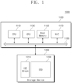
- FIG. 1 illustrates a block diagram of an example configuration of a computing system including a storage device according to embodiments of the inventive concepts.
- embodiments of the inventive concepts may provide a technology for minimizing a decrease in bandwidth and/or minimizing a transmission delay time of a storage device, which may occur in transmitting stream data, preferably in a system adopting an interface to apply a sharing technique of a memory resource.
- the storage device includes a solid state drive including a nonvolatile memory device and a buffer, the solid state drive receives a streaming access command including a logical block address (LBA) list and a chunk size, prefetches stream data from the nonvolatile memory block requested according to the LBA list and the chunk size without an additional command, and sequentially loads the prefetched stream data onto the buffer; and an in-storage computing block that accesses a streaming region registered on the virtual memory to sequentially read the stream data loaded onto the buffer in units of the chunk size.
- the buffer is mapped onto a virtual memory address of the streaming region.
- a computing system includes a host that manages a memory resource by using a virtual memory space; a storage device including a nonvolatile memory device and a buffer, the storage device receives a streaming access command, prefetches stream data from the nonvolatile memory device requested according to an LBA list and a chunk size included in the streaming access command without an additional command, and sequentially loads the prefetched stream data onto the buffer; and a field programmable gate array (FPGA) that accesses a streaming region registered at the virtual memory space to sequentially read the stream data loaded onto the buffer in units of the chunk size.
- FPGA field programmable gate array
- Still further embodiments of the inventive concepts provide an operation method of a storage device which is connected to a host using a virtual memory space and which includes a nonvolatile memory device and a buffer.
- the operation method includes mapping, by the storage device, a physical address of the buffer onto an address range corresponding to a streaming window of the virtual memory space; receiving, at the storage device, a streaming access command including an LBA list corresponding to stream data and a management unit of the stream data; prefetching, by the storage device, the stream data from the nonvolatile memory device with reference to the LBA list to sequentially load the prefetched stream data onto the buffer by the management unit; accessing, at a target device, the streaming window of the virtual memory space; redirecting the access to the streaming window to the buffer; and transferring the stream data sequentially loaded onto the buffer to the target device by the management unit.
- Embodiments of the inventive concepts provide an electronic system that includes a host device including a virtual memory space; and a storage device including nonvolatile memory, a buffer, a controller and an in-storage computing block.
- the controller receives a streaming access command, and loads stream data sequentially from the nonvolatile memory to the buffer with reference to the streaming access command.
- the in-storage computing block accesses the virtual memory space to sequentially read the stream data loaded in the buffer.
- circuits may, for example, be embodied in one or more semiconductor chips, or on substrate supports such as printed circuit boards and the like.
- circuits constituting a block may be implemented by dedicated hardware, or by a processor (e.g., one or more programmed microprocessors and associated circuitry), or by a combination of dedicated hardware to perform some functions of the block and a processor to perform other functions of the block.
- a processor e.g., one or more programmed microprocessors and associated circuitry
- Each block of the embodiments may be physically separated into two or more interacting and discrete blocks without departing from the scope of the inventive concepts.
- the blocks of the embodiments may be physically combined into more complex blocks without departing from the scope of the inventive concepts.
- FIG. 1 illustrates a block diagram of an example configuration of a computing system including a storage device according to embodiments of the inventive concept.
- Computing system 1000 may be one of a desktop computer, a laptop computer, a tablet computer, a smartphone, a wearable device, a server, an electric vehicle, home applications, etc.
- Computing system 1000 may be generally characterized as an electronic system, device or apparatus. Referring to FIG. 1 , the computing system 1000 may be roughly divided into a host device 1100 and a storage device 1200.
- the host device 1100 may perform various arithmetic/logical operations for the purpose of controlling overall operations of the computing system 1000.
- the host device 1100 may include a central processing unit (CPU) 1110, a graphic processing unit (GPU) 1130, a host memory 1150, a network interface card (NIC) 1170, and an interface circuit 1190.
- the host device 1100 may be a device, which includes one or more processor cores, such as for example a general-purpose CPU, a dedicated application specific integrated circuit (ASIC), or an application processor.
- processor cores such as for example a general-purpose CPU, a dedicated application specific integrated circuit (ASIC), or an application processor.
- the central processing unit 1110 may execute a variety of software (e.g., an application program, an operating system, and a device driver) loaded onto the host memory 1150.
- the central processing unit 1110 may execute an operating system (OS) and application programs.
- the central processing unit 1110 may be implemented for example with a homogeneous multi-core processor or a heterogeneous multi-core processor.
- the central processing unit 1110 may request the storage device 1200 to process a data intensive work load operation such as a data base scan operation.
- the storage device 1200 of the inventive concepts may perform in-storage computing to provide result data to the host device 1100.
- the graphics processing unit 1130 may perform various graphic operations in response to a request of the central processing unit 1110. That is, the graphics processing unit 1130 may convert process-requested data to data suitable for a display. A streaming access to the storage device 1200 may also be requested by the graphics processing unit 1130.
- the graphics processing unit 1130 may have an operation structure that is suitable for parallel processing in which similar operations are repeatedly processed. Accordingly, graphics processing units such as graphics processing unit 1130 are currently being developed to have a structure that may be used to perform various operations requiring high-speed parallel processing as well as graphic operations.
- the graphics processing unit 1130 that processes a general-purpose operation as well as a graphic processing operation is called a general purpose computing on graphics processing units (GPGPU).
- the GPGPU may for example be used to analyze a molecular structure, to decrypt a code, or to predict a meteorological change in addition to video decoding.
- the host memory 1150 may store data that are used to operate the computing system 1000.
- the host memory 1150 may store data processed or to be processed by the host device 1100.
- the host memory 1150 may include volatile/nonvolatile memory such as for example static random access memory (SRAM), dynamic RAM (DRAM), synchronous DRAM (SDRAM), phase-change RAM (PRAM), ferro-electric RAM (FRAM), magneto-resistive RAM (MRAM), and resistive RAM (ReRAM).
- SRAM static random access memory
- DRAM dynamic RAM
- SDRAM synchronous DRAM
- PRAM phase-change RAM
- FRAM ferro-electric RAM
- MRAM magneto-resistive RAM
- ReRAM resistive RAM
- the network interface card 1170 is a communication interface for connecting, e.g., an Ethernet switch (not illustrated) or an Ethernet fabric with the computing system 1000.
- an Ethernet switch corresponds to a wired LAN network
- the network interface card 1170 may be implemented with a wired LAN card.
- the network interface card 1170 may be implemented with hardware that processes a communication protocol corresponding to the wireless LAN.
- the interface circuit 1190 may provide a physical connection between the host device 1100 and the storage device 1200. That is, the interface circuit 1190 may convert a command, an address, data, etc. which correspond to various access requests generated from the host device 1100, so to be suitable for an interface manner with the storage device 1200.
- the interface circuit 1190 may be configured according to any of a variety of different communication protocols such as for example Universal Serial Bus (USB), Small Computer System Interface (SCSI), Peripheral Component Interface express (PCIe), Advanced Technology Attachment (ATA), parallel ATA (PATA), serial ATA (SATA), serial attached SCSI (SAS), and universal flash storage (UFS).
- USB Universal Serial Bus
- SCSI Small Computer System Interface
- PCIe Peripheral Component Interface express
- ATA Advanced Technology Attachment
- PATA parallel ATA
- SATA serial ATA
- SAS serial attached SCSI
- UFS universal flash storage
- the storage device 1200 may store data regardless of whether power is supplied.
- the storage device 1200 may include storage mediums such as for example solid state drives (SSDs), secure digital (SD ® ) cards, embedded multimedia cards (eMMC ® ), or the like.
- the storage device 1200 of the inventive concepts may include an in-storage computing block 1210 and an SSD 1230.
- the SSD 1230 may be characterized as an example of the storage medium.
- the in-storage computing block 1210 accesses the SSD 1230 in response to a request from the host device 1100.
- the in-storage computing block 1210 transfers a streaming access command (hereinafter referred to as "SA CMD") to the SSD 1230 in response to a data request from the host device 1100.
- SA CMD a streaming access command
- the streaming access command SA_CMD includes information of an LBA list, a stream ID, a chunk size, and possibly a priority, etc.
- the in-storage computing block 1210 processes within the storage device 1200 stream data provided from the SSD 1230 in response to the streaming access command. Result data processed by the in-storage computing block 1210 are returned to the host device 1100.
- the above operation of the in-storage computing block 1210 makes it possible to markedly improve (or minimize) a decrease in a bandwidth due to the exchange of stream data between the storage device 1200 and the host device 1100.
- the SSD 1230 stores and/or outputs data in response to a request provided from the host device 1100 and/or the in-storage computing block 1210.
- the SSD 1230 provides stream data in units of a requested data size in response to the streaming access command (e.g., a streaming read command or a streaming write command).
- the streaming access command e.g., a streaming read command or a streaming write command.
- the SSD 1230 allows a DMA engine (not illustrated) of the in-storage computing block 1210 to sequentially read data stored in the buffer. This will be described in detail hereinafter with reference to drawings.
- a configuration of the storage device 1200 including the in-storage computing block 1210 of the inventive concepts, and a configuration of the computing system 1000 in which the storage device 1200 is included have been briefly described.
- the storage device 1200 of embodiments efficiently processes stream data by using the streaming access command.
- FIG. 2 illustrates a block diagram of an example configuration of a host and a storage device of FIG. 1 .
- the host device 1100 and the storage device 1200 constitute the computing system 1000.
- the host device 1100 may include the central processing unit 1110, the host memory 1150, the interface circuit 1190, and a memory management unit 1160 for the purpose of processing stream data. It should be understood that the host device 1100 may further include components such as the graphics processing unit 1130 and/or the network interface card 1170. However, for convenience of description, some functions of the components of the host device 1100 may not be here described, and/or some of the components may not be illustrated.
- the central processing unit 1110, the host memory 1150, and the interface circuit 1190 may be substantially the same as those of FIG. 1 , and thus, additional description may be omitted to avoid redundancy.
- the host device 1100 maps a buffer 1235 of the SSD 1230 onto a virtual memory space of the host device 1 100.
- a storage device such as the SSD 1230 does not open the buffer 1235, which is a memory space for direct memory access (DMA), for any other device.
- DMA direct memory access
- the host device 1100 registers the buffer 1235 at a virtual memory space to manage the buffer 1235 through one map, and thus, the buffer 1235 is freely accessible by a DMA engine 1211 of the in-storage computing block 1210.
- the host device 1100 may include the memory management unit 1160.
- the buffer 1235 is opened to an external device for transmission of stream data by mapping a physical address region of the buffer 1235 of the SSD 1230 onto a virtual memory space. An access of an external device to the virtual memory space may be redirected to the buffer 1235 by the memory management unit 1160.
- the storage device 1200 processes data provided from the SSD 1230 in an in-storage computing manner in response to a request of the host device 1 100.
- the storage device 1200 returns a result of the in-storage computing to the host device 1100.
- the storage device 1200 includes the in-storage computing block 1210, the SSD 1230, and a host interface 1250.
- the in-storage computing block 1210 may include the DMA engine 1211 and a kernel memory 1213.
- the in-storage computing block 1210 may be implemented with at least one of a processor or processor core, a field programmable gate array (FPGA), and an application specific integrated circuit (ASIC).
- the in-storage computing block 1210 provides the streaming access command to the SSD 1230 in response to a request of the host device 1100.
- the in-storage computing block 1210 processes stream data transferred from the SSD 1230 in the in-storage computing manner and transfers the processed data to the host device 1100.
- the DMA engine 1211 reads stream data of a chunk size loaded onto the buffer 1235 of the SSD 1230 and transfers the read data to the kernel memory 1213.
- the chunk size defines a management unit of the stream data.
- the SSD 1230 loads data, which are read from a storage medium in the unit of a chunk size defined by a command, onto the buffer 1235 in response to the streaming read command from the in-storage computing block 1210.
- the buffer 1235 is accessible by the DMA engine 1211 of the in-storage computing block 1210.
- the SSD 1230 programs data transferred in the unit of a chunk size in the buffer 1235 in response to a steaming write command from the in-storage computing block 1210.
- the host interface 1250 may bes provided as a physical communication channel of the storage device 1200, which may be used for data exchange with the host device 1100.
- the host interface 1250 may have an interfacing protocol supporting DMA functions of the in-storage computing block 1210 and the SSD 1230.
- the buffer 1235 of the SSD 1230 may be managed in the virtual memory space by the memory management unit 1160 of the host device 1100 and the host interface 1250.
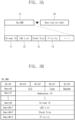
- FIGS. 3A, 3B , and 3C illustrate diagrams of a streaming access command according to embodiments of the inventive concepts.
- FIG. 3A shows attributes constituting the streaming access command SA_CMD.
- FIG. 3B is a table showing a way to configure the streaming access command SA_CMD in an NVMe interface protocol.
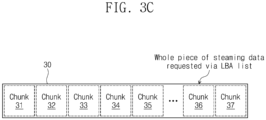
- FIG. 3C shows stream data managed in units of chunk size.
- NVMe NVM Express
- a streaming request provided from the outside may include the streaming access command SA_CMD (corresponding to reference numeral "10") and a destination address (Addr) 20.
- the streaming access command SA_CMD may be a streaming read command SR_CMD or a steaming write command SW_CMD.
- the destination address 20 may indicate a memory position to which a DMA engine (not illustrated) included in the in-storage computing block 1210 will finally transfer requested stream data.
- the streaming access command SA_CMD may include a stream ID 11, an LBA list 12, a chunk size 13, and a priority 14.
- the stream ID 11 includes identifier (ID) information for identifying multi-stream data.
- ID identifier
- the stream ID 11 may be assigned to the multi-stream data when the multi-stream data are generated and/or in the process of transferring the multi-stream data.
- a streaming window may be assigned for each stream ID 11.
- the LBA list 12 may be a list of LBAs targeted for an access request through the streaming access command SA_CMD. For example, when LBAs LBA0 to LBA10000 are transferred through the LBA list 12, preferably (i.e., optionally) a physical address region of the SSD 1230 (refer to FIG. 2 ), which corresponds to the LBAs LBA0 to LBA10000, is accessed.
- a streaming command may be provided by information such as an LBA start address and/or a sector count.
- the streaming access command SA_CMD of the inventive concepts may simultaneously provide a list of all LBAs corresponding to streaming data, and thus may minimize an iterative command transfer.
- the chunk size 13 indicates a transfer or input/output unit of stream data between the buffer 1235 of the SSD 1230 and the in-storage computing block 1210, and/or between the buffer 1235 and the external device.
- a prefetch operation is performed on the buffer 1235 in the unit of the chunk size 13, and a DMA transfer operation is made from the buffer 1235 to a destination in the unit of the chunk size 13.
- the chunk size 13 is matched with a size of a streaming window to be assigned for stream data on the virtual memory space to be described later.
- the priority 14 includes priority information of the stream ID 11.
- commands may be arranged in a 32-bit (Dword) unit.
- the streaming access command SA_CMD may include field regions (e.g., Dword0 and Dword1) that normal commands have in common, and/or field regions such as DwordN to DwordN+3 for the streaming access command SA_CMD of embodiments.
- the field regions Dword0 and Dword1 that normal commands have in common may include for example various elements CID, Fuse, Opcode, and Namespace ID.
- CID command ID
- Fuse Opcode
- Namespace ID may indicate a code value specifying an operation attribute of a command.
- the "Namespace ID” may include identifier information of a namespace.
- the field regions DwordN to DwordN+3 for composing the streaming access command SA_CMD of embodiments may include a stream ID (DwordN), an LBA list (DwordN+1), a chunk size (DwordN+2), and/or a priority (DwordN+3). Attributes of the stream ID, the LBA list, the chunk size, and/or the priority may be the same as those described with reference to FIG. 3A .
- a way to construct the stream ID, the LBA list, the chunk size, and the priority for the streaming access command SA_CMD may be variously implemented.
- a reserved field of a command set associated with the NVMe protocol may be used to construct a streaming access command (SA_CMD) set.
- fields newly defined to construct a streaming access command (SA_CMD) set may be added to construct the streaming access command SA_CMD.
- the whole piece of data 30 requested for streaming may for example be managed in the unit of a plurality of chunks 31 to 37.
- the whole piece of requested data may be defined based on an LBA list included in the streaming access command SA_CMD.
- the whole piece of data 30 may include a plurality of partitioned data each having a chunk size.
- the storage device 1200 may manage data divided in the unit of a chunk size for the purpose of outputting or receiving the whole piece of data 30.
- FIG. 4 illustrates a memory map of a virtual memory space of a host.
- a virtual memory space 1161 of the host device 1100 includes a memory region of the buffer 1235 of the SSD 1230.
- Memory spaces of various peripheral devices are registered in the virtual memory space 1161 of the host device 1100, which may be managed by the memory management unit 1160.
- the computing system 1000 including the storage device 1200 having an in-storage computing function of embodiments a partial memory region or the whole memory region of the buffer 1235 in the SSD 1230 is registered at the virtual memory space 1161.
- the host memory 1150 that is provided as a main memory of the host device 1100 may be a shared memory accessible by peripheral devices, but the buffer 1235 of storage such as the SSD 1230 may not be shared by peripheral devices due to security or any other causes. Accordingly, it is difficult for the DMA engine 1211 of the in-storage computing block 1210, or a DMA engine of the host device 1100 or each peripheral device, to access the buffer 1235 directly.
- the buffer 1235 of the SSD 1230 is advantageously shared by a DMA engine of a target device.
- the virtual memory space 1161 of the host device 1100 is used such that the buffer 1235 of the SSD 1230 is shared by the DMA engine of the target device.
- registration may be performed by using a base address register BAR.
- the host device 1100 and/or peripheral devices which access the buffer 1235, accesses an address registered at the virtual memory space 1161.
- the virtual address is redirected to the buffer 1235 by the memory management unit 1160.
- the in-storage computing block 1210, the host device 1100, and/or any other peripheral devices share the buffer 1235 of the SSD 1230 through the virtual memory space 1161.
- the virtual memory space 1161 of the host device 1100 includes a streaming region 1162 that corresponds to a virtual address range for managing stream data of the buffer 1235 of the SSD 1230.
- the streaming region 1162 may include at least one streaming window corresponding to a chunk size included in the streaming access command SA_CMD.
- the streaming window is provided in an input/output unit corresponding to a stream identifier ID included in the streaming access command SA_CMD. That is, streaming windows, the number of which corresponds to the number of stream IDs of multi-stream data, may be assigned to the streaming region 1162.
- streaming windows may be set to the virtual memory space 1161 as much as the number of stream IDs of stream data to be read from or programmed in the SSD 1230.
- the DMA engine 1211 of the in-storage computing block 1210 intends to read data corresponding to a streaming window SW1
- the DMA engine 1211 may access a virtual memory space corresponding to a chunk size CS and/or an address 0xFFFF of the virtual memory space 1161.
- the access of the DMA engine 1211 is redirected to the buffer 1235 of the SSD 1230 by the memory management unit 1160.
- FIG. 5 illustrates a block diagram of an example configuration of an SSD according to embodiments of the inventive concepts.
- the SSD 1230 may include an SSD controller 1231, a nonvolatile memory device(s) 1233, and/or the buffer 1235.
- the SSD controller 1231 may provide interfacing between an external device and the SSD 1230.
- the SSD controller 1231 may access the nonvolatile memory device 1233 with reference to a stream ID, an LBA list, and/or a chunk size CS included in the streaming access command SA_CMD provided from the outside.
- the SSD controller 1231 may prefetch data corresponding to the LBA list from the nonvolatile memory device 1233 in the unit of the chunk size CS and may load the prefetched data onto the buffer 1235.
- the SSD controller 1231 may program write data loaded onto the buffer 1235 from the outside in the unit of the chunk size CS in the nonvolatile memory device 1233.
- the SSD controller 1231 may include a streaming manager 1232 for managing the nonvolatile memory device 1233 and/or the buffer 1235 based on the streaming access command SA_CMD.
- the streaming manager 1232 may parse the streaming access command SA_CMD and prefetch stream data corresponding to the LBA list from the nonvolatile memory device 1233 to the buffer 1235 in the unit of the chunk size CS.
- the streaming manager 1232 may manage the buffer 1235 such that a target device reads stream data ST_Data from the buffer 1235 in the unit of the chunk size CS.
- FIG. 6 illustrates a block diagram of an example configuration of an SSD controller of FIG. 5 .
- the SSD controller 1231 may include a processor 121, a working memory 123, an interface 125, a buffer manager 127, and/or a flash interface 129.
- the streaming manager 1232 that may process a streaming command of embodiments may be implemented with a firmware or software module for example.
- the processor 121 may execute the streaming manager 1232 loaded onto the working memory 123. As the streaming manager 1232 is executed, the streaming manager 1232 may transfer various control information necessary to perform a read/write operation to registers of the interface 125 and/or flash interface 129. For example, in the case where the streaming access command SA_CMD is received from the outside, the streaming access command SA_CMD is stored in a command register (not illustrated) of the interface 125. The interface 125 may notify the processor 121 that the read/write command is input to the processor 121, based on the stored command. The processor 121 may parse the streaming access command SA_CMD transferred to the interface 125 to control the buffer manager 127 and/or the flash interface 129.
- the processor 121 reads stream data corresponding to an LBA list from the nonvolatile memory device 1233.
- the processor 121 prefetches stream data from the nonvolatile memory device 1233 in the units of the chunk size CS and loads the prefetched stream data onto the buffer 1235.
- the processor 121 may inform an external device of a head pointer and/or a tail pointer of the stream data loaded onto the buffer 1235.
- the processor 121 may detect an access of an external device to the buffer 1235 to manage the head pointer and/or the tail pointer of the buffer 1235.
- the processor 121 may manage a streaming window of the virtual memory space 1161, onto which requested stream data is loaded in the unit of a chunk size.
- the working memory 123 may store data that are used to drive the SSD controller 1231.
- various firmware to be executed by the SSD controller 1231 may be loaded onto the working memory 123.
- a flash translation layer (FTL) to be executed by the processor 121 or a firmware image such as the streaming manager 1232 of embodiments may be loaded onto the working memory 123 and may be executed by the processor 121.
- FTL flash translation layer
- the interface 125 may provide a physical connection between the host device 1100 and/or an external device (e.g., through the host interface 1250 as shown in FIG. 2 ) and/or the SSD 1230. That is, the interface 125 may provide interfacing with the SSD 1230, which complies with a bus format of the host device 1100.
- the bus format of the host device 1100 may include for example at least one of Universal Serial Bus (USB), Small Computer System Interface (SCSI), Peripheral Component Interface express (PCIe), Advanced Technology Attachment (ATA), parallel ATA (PATA), serial ATA (SATA), a serial attached SCSI (SAS), NVMe, and NVMe over Fabrics (NVMe-oF).
- the buffer manager 127 may control read and write operations of the buffer 1235 (refer to FIG. 5 ). For example, the buffer manager 127 temporarily stores write data or read data in the buffer 1235. For example, the buffer manager 127 may identify and manage a memory region of the buffer 1235 in the unit of a stream under control of the processor 121. Under control of the processor 121, the buffer manager 127 may update a head pointer or a tail pointer of the buffer 1235 implemented with a ring buffer or a circular buffer and may output the updated pointer to the outside.
- the flash interface 129 may exchange data with the nonvolatile memory device 1233.
- the flash interface 129 may write data transferred from the buffer 1235 in the nonvolatile memory device 1233.
- the flash interface 129 may transfer the data read from the nonvolatile memory device 1233 to the buffer 1235.
- the SSD controller 1231 may manage the buffer 1235 in the unit of the chunk size CS in response to the streaming access command SA_CMD.
- Status information of the buffer 1235 may be transferred to the outside of the SSD 1230 by the SSD controller 1231.
- the status information of the buffer 1235 transferred to the outside may be referenced for a DMA operation of a target device that transfers data in the unit of the chunk size CS.
- FIG. 7 illustrates a flowchart of an operation of a streaming manager of FIG. 6 according to embodiments of the inventive concepts.
- a control operation for transferring stream data of the streaming manager 1232 of the SSD 1230 starts.
- the SSD 1230 may receive the streaming access command SA_CMD provided from the host device 1100 or any other peripheral device.
- the streaming access command SA_CMD may include values of a stream ID, an LBA list, a chunk size, and a priority.
- a destination address of stream data to be transferred may be provided together with the streaming access command SA_CMD.
- a configuration of the streaming access command SA_CMD of the inventive concepts is not limited thereto. It should be well understood that various parameters for efficiently controlling the buffer 1235 and a prefetch operation for processing of multi-stream data may be included in or added to the streaming access command SA_CMD.
- the streaming manager 1232 may parse the received streaming access command SA_CMD.
- the streaming manager 1232 may identify the whole piece of data to be read and data output just prior to receipt of the streaming access command SA_CMD, based on an LBA list obtained by parsing the streaming access command SA_CMD.
- the streaming manager 1232 may set a head pointer HP and/or a tail pointer TP of the buffer 1235, based on information about the data output until just prior to receipt of the streaming access command SA_CMD.
- the host device 1100 or an external device accesses a streaming window of the virtual memory space 1161 based on the head pointer HP and/or the tail pointer TP of the buffer 1235, the access of the host device 1100 and/or the external device may be redirected to the buffer 1235 by the memory management unit 1160.
- the streaming manager 1232 may update or register the streaming window at the streaming region 1162 reserved on the virtual memory space 1161. That is, the streaming window may correspond to a size (i.e., a chunk size) of data, which are exchanged between the buffer 1235 and the target device, on the virtual memory space 1161.
- a size i.e., a chunk size
- the streaming manager 1232 may prefetche requested data from the nonvolatile memory device 1233.
- the prefetched data may be stored in the buffer 1235.
- the head pointer HP of the buffer 1235 may be updated after the prefetched data are stored in the buffer 1235.
- the streaming manager 1232 may move the tail pointer TP of the buffer 1235.
- the streaming manager 1232 may determine whether the whole piece of data requested through the streaming access command SA_CMD are transferred to a destination address. That is, the streaming manager 1232 may compare the provided LBA list with the data already output to determine whether the requested stream data are completely serviced. Preferably, when it is determined that the requested data are completely transferred to the target device (Yes in S160), overall operations of the SSD 1230 corresponding to the streaming access command SA_CMD end. Preferably, when it is determined that data from among the requested data are not yet transferred to the target device (No in S160), the process returns to operation S150.
- FIG. 8 illustrates a block diagram of a path over which data are transferred according to a streaming read command, according to embodiments of the inventive concepts.
- the SSD 1230 prefetches data from the nonvolatile memory device 1233 to the buffer 1235 based on LBA lists of the streaming access command SA_CMD.
- the in-storage computing block 1210 may access the streaming window Streaming Window #1 registered at the virtual memory space 1161 of the host device 1100 such that data of the buffer 1235 are transferred directly to an SRAM (i.e., kernel memory) 1213 of a kernel 1212.
- SRAM i.e., kernel memory
- the SSD 1230 may read data from the nonvolatile memory device 1233 based on an LBA list and a chunk size. This operation may be controlled by the streaming manager 1232 that is driven on the SSD 1230.
- the prefetch from the nonvolatile memory device 1233 to the buffer 1235 may be performed with reference to the chunk size CS provided by the streaming access command SA_CMD. That is, data may be loaded onto and/or output from the buffer 1235 in the unit of the chunk size CS. Accordingly, in the case where the buffer 1235 is managed in the form of a ring buffer, the head pointer HP and/or the tail pointer TP of the buffer 1235 may move in the unit of a chunk size.
- the data structure of the buffer 1235 may be variously changed or modified without limitation to the example of FIG. 8 .
- Data prefetched to the buffer 1235 may be enqueued between a head and a tail of a circular queue.
- the prefetched data may be enqueued in the circular queue in the unit of a chunk size.
- the streaming manager 1232 of the SSD 1230 may manage the streaming region 1162 and a streaming window registered at the virtual memory space 1161.
- the streaming region 1162 may allow an external device or the host device 1100 to access the stream data loaded onto the buffer 1235.
- a peripheral device and/or the in-storage computing block 1210 may access the first streaming window Streaming Window #1 registered at the virtual memory space 1161 without restriction.
- the first streaming window Streaming Window #1 and the second streaming window Streaming Window #2 correspond to different streaming IDs, respectively. That is, chunks of different streaming ID prefetched to the buffer 1235 may be assigned to the first streaming window Streaming Window #1 and the second streaming window Streaming Window #2, respectively.
- the access may be redirected to a memory region of the buffer 1235, in which a corresponding chunk is stored. This redirection may be managed by the memory management unit 1160 or the central processing unit 1110 of the host device 1100.
- a streaming window may enable an access to enqueued data of a chunk size.
- Data that are loaded onto the buffer 1235 of the SSD 1230 in the unit of a chunk size by the streaming access command SA_CMD may be transferred to a destination, such as the SRAM 1213 of the kernel 1212, by the in-storage computing block 1210. That is, as the buffer 1235 may be mapped onto the virtual memory space 1161 of the host device 1100, the buffer 1235 may be accessed by the in-storage computing block 1210 without restriction. As the buffer 1235 is mapped onto the virtual memory space 1161 of the host device 1100, the DMA engine 1211 of the in-storage computing block 1210 may transfer stream data to a destination memory (e.g., the SRAM 1213) without passing through a DRAM 1215.
- a destination memory e.g., the SRAM 1213
- the in-storage computing block 1210 may repeatedly obtain enqueued data of a chunk size through the streaming window.
- the SSD 1230 may update a pointer of the buffer 1235 corresponding to a streaming window (e.g., a first streaming window) registered at the virtual memory space 1161 whenever the in-storage computing block 1210 obtains enqueued data.
- a streaming window e.g., a first streaming window
- the SSD 1230 may change a value of the head pointer HP of the buffer 1235 such that the head pointer HP of the buffer 1235 directs enqueued data to be read next.
- the in-storage computing block 1210 may access the virtual memory space 1161 of the host device 1100 corresponding to the streaming window Streaming window #1. In this case, the access may be redirected to a region of the buffer 1235 corresponding to the head pointer HP by the central processing unit 1110 of the host device 1100 or the memory management unit 1160 provided separately. Stream data of a chunk size provided from the buffer 1235 may be transferred directly to the SRAM 1213 of the kernel 1212.
- the head pointer HP of the circular queue may be updated to direct next enqueued data.
- the SSD 1230 may prefetch different data from a memory device to the buffer 1235.
- the tail pointer TP of the circular queue may be updated to direct the newly prefetched data.
- the in-storage computing block 1210 may sequentially obtain stream data divided in the unit of a chunk size by using the single streaming access command SA_CMD. In this case, until the whole piece of intended data are obtained, the in-storage computing block 1210 may repeatedly obtain enqueued data of a chunk size through the streaming window. In the case where the in-storage computing block 1210 obtains the whole piece of intended data, a streaming read operation may be completed.
- an access may be requested from the in-storage computing block 1210 before stream data are prefetched to the buffer 1235 of the SSD 1230.
- the SSD 1230 may delay processing of the request of the in-storage computing block 1210 until data are prefetched to the buffer 1235.
- an additional streaming read command may be received in a state where the circular queue is fully filled with prefetched data. In this case, the SSD 1230 may delay processing of the additional streaming read command until all or a part of the circular queue is empty.
- stream data may be buffered in the buffer 1235 of the SSD 1230, instead of being transferred to the host memory 1150 (refer to FIG. 2 ) of the host device 1100. Accordingly, a memory space of the host memory 1150 of the inventive concept may not be required. Overhead of the computing system 1000 may thus be decreased.
- the SSD 1230 may buffer stream data divided in the unit of a chunk size instead of buffering the whole piece of data at the same time. Accordingly, a buffer resource of the SSD 1230, which may be characterized as a memory resource, may be efficiently used.
- the buffer 1235 of the SSD 1230 may be accessible from an external device, and divided data of a chunk size may be buffered in the accessible buffer 1235.
- the in-storage computing block 1210 may manage the whole piece of intended data obtained from the buffer 1235 of the SSD 1230 in the SRAM 1213 of the kernel 1212. This may prevent the DMA engine 1211 from repeatedly issuing a memory access request, thus improving the performance of the in-storage computing block 1210.
- the buffer 1235 of the SSD 1230 may include a memory region that is accessible from an external device, and prefetched data of a chunk size may be managed in the accessible memory region. In some cases, all the regions of the buffer 1235 of the SSD 1230 may be accessible from the external device. Alternatively, only some regions of the buffer 1235 of the SSD 1230 may be accessible from the external device, and the remaining regions may be inaccessible for security.
- a latency may increase when data are exchanged, but a bandwidth to exchange each divided data may increase, and the performance of communication may be improved.
- a latency may decrease when data are exchanged.
- the chunk size may be appropriately selected in consideration of the above conditions.
- a buffer may be implemented with a high-capacity buffer, and a plurality of data may be enqueued at the same time, and the performance of communication may be improved.
- the buffer may be implemented with a small-capacity buffer. The size of the circular queue may be appropriately selected in consideration of the above conditions.
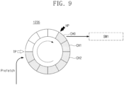
- FIG. 9 illustrates a diagram showing how to manage a buffer having a circular queue shape, according to embodiments of the inventive concepts.
- a region of the buffer 1235 in which stream data are stored may be managed in the form of a ring buffer of a circular queue type.
- data of a chunk size prefetched from the nonvolatile memory device 1233 may be stored in the buffer 1235 as chunk data CH0, CH1, CH2, etc.
- the streaming manager 1232 or the buffer manager 127 updates the tail pointer TP.
- chunk data CH0 are transferred to an external device and/or the in-storage computing block 1210 which accesses the streaming window SW1
- the head pointer HP of the buffer 1235 may move as much as a chunk size.
- an access to the streaming window SW1 may be redirected to chunk data CH1 corresponding to a position of the updated head pointer HP.
- pointers of the buffer 1235 may move.
- FIG. 10 illustrates a diagram of a streaming read command for in-storage computing performed in a storage device and a response of the storage device to the streaming read command, according to embodiments of the inventive concepts.
- the host device 1100 requests specific data from the storage device 1200 (e.g., a data intensive work load operation such as a data base scan operation).
- the host device 1100 transfers a data request (Data Request) to the storage device 1200.
- the data request that the host device 1100 transfers may be a request for data base scan of data stored in the storage device 1200.
- the request for the data intensive workload is transferred to the in-storage computing block 1210 provided in the storage device 1200.
- a description is given as the host device 1100 transfers the data request.
- the data request may be issued from various peripheral devices such as for example from the CPU 1110, the GPU 1130, or the network interface card 1170 in the host device 1100, or from a field programmable gate array (FPGA), an ASIC, or the like provided as a peripheral device.
- FPGA field programmable gate array
- the in-storage computing block 1210 provided in the storage device 1200 transfers the streaming read command of embodiments of the inventive concepts to the SSD controller 1231 of the SSD 1230.
- the in-storage computing block 1210 may additionally provide a destination address together with the streaming read command.
- the streaming read command includes a stream ID, an LBA list, a chunk size CS, and optionally a priority.
- the SSD controller 1231 transfers a prefetch command for reading data stored in the nonvolatile memory device 1233 in response to the streaming read command.
- the SSD controller 1231 controls the nonvolatile memory device 1233 such that data of the chunk size CS are read from the nonvolatile memory device 1233 by using address information collected from the LBA list.
- the nonvolatile memory device 1233 may output stream data of the chunk size CS to the buffer 1235 in response to a prefetch command from the SSD controller 1231. Data corresponding to a plurality of chunk sizes CS may be accumulated in the buffer 1235.
- a streaming window registered at the virtual memory space 1161 may be accessed by the DMA engine 1211 of the in-storage computing block 1210.
- the access may be redirected to a position corresponding to the head pointer HP of the buffer 1235, and stream data corresponding to a chunk Chunk 0 enqueued in the buffer 1235 may be transferred to the in-storage computing block 1210.
- the stream data corresponding to the chunk Chunk 0 output from the buffer 1235 may be transferred directly to the SRAM 1213 provided as a kernel memory.
- the SSD controller 1231 may transfer a prefetch command to the nonvolatile memory device 1233 in response to the data output of the buffer 1235.
- the SSD controller 1231 may perform a prefetch operation in consideration of stream data already transferred and stream data to be transferred next.
- the nonvolatile memory device 1233 may output stream data of the chunk size CS to the buffer 1235 under control of the SSD controller 1231.
- a streaming window registered at the virtual memory space 1161 may be accessed by the DMA engine 1211 of the in-storage computing block 1210.
- the access may be redirected to a position corresponding to the head pointer HP of the buffer 1235, and stream data corresponding to a chunk Chunk_1 enqueued in the buffer 1235 may be transferred to the in-storage computing block 1210.
- the stream data corresponding to the chunk Chunk_1 output from the buffer 1235 may be transferred directly to the SRAM 1213 provided as a kernel memory.
- the prefetch operation of the chunk unit and the transfer to the in-storage computing block 1210, which are described above, may be repeated until the last chunk Chunk_N-1 is repeated.
- the SSD controller 1231 may perform a prefetch operation from the nonvolatile memory device 1233 to the buffer 1235 in response to the data output of the buffer 1235.
- the SSD controller 1231 may perform a prefetch operation in consideration of stream data already transferred and stream data to be transferred next.
- the nonvolatile memory device 1233 may output the last stream data Chunk_N-1 defined in the LBA list to the buffer 1235 under control of the SSD controller 1231.
- a streaming window registered at the virtual memory space 1161 may be accessed by the DMA engine 1211 of the in-storage computing block 1210.
- the access may be redirected to a position corresponding to the head pointer HP of the buffer 1235, and stream data corresponding to the last chunk Chunk_N-1 enqueued in the buffer 1235 may be transferred to the in-storage computing block 1210.
- the in-storage computing block 1210 may collect the obtained stream data to perform in-storage computing. For example, the in-storage computing block 1210 may perform processing, such as a data base scan operation, on the obtained stream data. When the in-storage computing is completed, the in-storage computing block 1210 may finally select a value requested from the host device 1100.
- the in-storage computing block 1210 may return only data selected by a result of the in-storage computing to the host device 1100.
- Data input/output between the host device 1100 and the storage device 1200 described above may only include a data request of operation S10 and a return of requested data of operation S70. Accordingly, in the case of using a streaming access command according to embodiments of the inventive concepts, a decrease in a bandwidth of the storage device 1200 in which a data intensive workload operation is performed may be markedly improved.
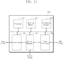
- FIG. 11 illustrates a block diagram of an SSD controller of FIG. 5 , according to embodiments of the inventive concepts.
- the SSD controller 1231 may include the processor 121, the working memory 123, the interface 125, the buffer manager 127, the flash interface 129, and/or the streaming manager 1232 implemented as a hardware block.
- the processor 121, the working memory 123, the interface 125, the buffer manager 127, the flash interface 129 may be substantially the same as those described with reference to FIG. 6 , and thus, additional description will be omitted to avoid redundancy.
- the streaming access command SA_CMD may be stored in a command register (not illustrated) of the interface 125.
- the interface 125 may notify the processor 121 that the read/write command is input to the processor 121, based on the stored command.
- the streaming manager 1232 may prefetch requested data by using an LBA list from the nonvolatile memory device 1233 to the buffer 1235 in the unit a chunk size in response to the streaming access command SA_CMD.
- the streaming manager 1232 may transfer a status of the buffer 1235 to the outside and may allow a target device to freely access the buffer 1235.
- the streaming manager 1232 may read stream data corresponding to the LBA list from the nonvolatile memory device 1233.
- the streaming manager 1232 may prefetch stream data from the nonvolatile memory device 1233 in the unit of the chunk size CS and load the prefetched stream data onto the buffer 1235.
- the streaming manager 1232 may inform an external device of a head pointer and/or a tail pointer of the stream data loaded onto the buffer 1235.
- the streaming manager 1232 may detect an access of an external device to the buffer 1235 to manage the head pointer and/or the tail pointer of the buffer 1235.
- the streaming manager 1232 may manage a streaming window of the virtual memory space 1161, onto which requested stream data may be loaded in the unit of a chunk size.
- the SSD controller 1231 may manage the buffer 1235 in the unit of the chunk size CS in response to the streaming access command SA_CMD.
- Status information of the buffer 1235 may be transferred to the outside of the SSD 1230 by the streaming manager 1232.
- the status information of the buffer 1235 transferred to the outside may be referenced for a DMA operation of a target device that transfers data in the unit of the chunk size CS.
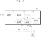
- FIG. 12 illustrates a block diagram of a configuration of a streaming manager of FIG. 11 .
- the streaming manager 1232 may include a command parser 1410, an LBA list manager 1420, a streaming window manager 1430, a prefetcher 1440, a streaming buffer manager 1450, and/or an access detector 1460.
- the command parser 1410 may parse the streaming access command SA_CMD.
- the command parser 1410 may obtain information, such as LBA lists and a chunk size, from the parsed streaming access command SA_CMD.
- the command parser 1410 may provide the obtained information to the LBA list manager 1420 and the streaming window manager 1430.
- the LBA list manager 1420 may manage the following information based on the LBA list obtained from the command parser 1410: the whole piece of data to be read from the nonvolatile memory device 1233 and/or data previously read (and thus enqueued in a circular queue).
- the streaming window manager 1430 may manage a streaming window for providing stream data divided from the whole piece of data to an external device, preferably based on the LBA list obtained from the command parser 1410 and/or the information managed by the LBA list manager 1420. For example, the streaming window manager 1430 may register a streaming window at a virtual memory space such that enqueued data are provided to the external device and may manage the registered streaming window. The streaming window manager 1430 may provide information for managing a streaming window to the memory management unit 1160 of the host device 1100.
- the streaming buffer manager 1450 may manage a memory region of the buffer 1235, which is used for stream data.
- the streaming buffer manager 1450 may manage a status and an operation of the buffer 1235 such that stream data are enqueued and dequeued with regard to the streaming window managed by the streaming window manager 1430.
- the streaming buffer manager 1450 may adopt a data structure of a circular queue, but embodiments of the inventive concepts are not limited to this example.
- the prefetcher 1440 may prefetch data read from a memory device to the buffer 1235, based on information managed by the LBA list manager 1420.
- the prefetcher 1440 may prefetch data read from the nonvolatile memory device 1233 in the unit of a chunk size.
- the prefetcher 1440 may prefetch data to a memory region of the buffer 1235, which may be directed by the streaming buffer manager 1450.
- the access detector 1460 may detect that the external device accesses the streaming window.
- the access detector 1460 may detect an access of the external device or the host device 1100 to the buffer 1235, and the head pointer HP of the buffer 1235 may be updated according to a detection result.
- the prefetch operation from the nonvolatile memory device 1233 to the buffer 1235 may be performed according to the detection result of the access detector 1460.
- the streaming manager 1232 may be provided within the storage device 1200.
- the SSD 1230 may perform the above-described streaming write and read operations under control of the SSD controller 1231.
- the SSD controller 1231 may include the streaming manager 1232.
- the streaming manager 1232 may be implemented with a program code of software and/or firmware, and a processor core of the SSD controller 1231 may execute an instruction set of the program code to provide the streaming read operation and the streaming write operation.
- the streaming manager 1232 may be implemented with hardware circuits (e.g., an analog circuit, a logic circuit, an FPGA, and an ASIC) configured to perform the above-described operations.
- the hardware circuits may be included in the SSD controller 1231 or may be provided outside the SSD controller 1231.
- the streaming manager 1232 may be provided in a hybrid form of software and hardware.
- the streaming manager 1232 may be provided outside the storage device 1200.
- the streaming manager 1232 may be provided at an input/output stage of a storage device, thus existing between the storage device 1200 and an external device.
- the streaming manager 1232 may perform the above-described operations on data input to the storage device 1200 and/or data output from the storage device 1200.
- implementation of the streaming manager 1232 may be variously changed or modified.
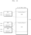
- FIG. 13 illustrates a diagram showing a method of assigning a streaming region in a virtual memory space of a host according to embodiments of the inventive concepts.
- memory regions of buffers 1235, 1245, and 1255 of a plurality of SSDs including first SSD (SSD1) 1230, second SSD (SSD2) 1240, and third SSD (SSD3) 1250 may be registered at the virtual memory space 1161 of the host device 1100.
- the buffer 1235 may be mapped onto a first streaming region (Streaming Region1) 1162 of the virtual memory space 1161, preferably for the purpose of managing stream data enqueued in the buffer 1235 of the first SSD 1230.
- the number of streaming windows assigned to the first streaming region 1162 may be as much as (or correspond in number to) the number of streaming IDs of stream data to be stored in the buffer 1235. That is, the first streaming region 1162 may be assigned to a virtual memory that is used for the one first SSD 1230 to exchange stream data with the outside.
- the access may be redirected to the buffer 1235 of the first SSD 1230 by the memory management unit 1160 of the host device 1100.
- the buffers 1245 and 1255 of the second and third SSDs 1240 and 1250 may be mapped onto a second streaming region (Streaming Region2) 1164 of the virtual memory space 1161. That is, the one second streaming region 1164 may cover stream data that are input to or output from the buffers 1245 and 1255 of the second and third SSDs 1240 and 1250.
- the second and third SSDs 1240 and 1250 are implemented in the form of RAID (Redundant Array of Independent Disks or Redundant Array of Inexpensive Disks)
- this mapping of the virtual memory space 1161 may be possible.
- memory regions of the buffers 1235, 1245, and 1255 may be registered at the virtual memory space 1161 by using the base address register (BAR).
- BAR base address register
- an external device accesses a virtual address assigned on the virtual memory space 1161
- an access to any one of the buffers 1235, 1245, and 1255 may be redirected by the memory management unit 1160.
- the in-storage computing block 1210, the host device 1100, and/or any other peripheral devices may share the buffers 1235, 1245, and 1255 through the virtual memory space.
- FIG. 14 illustrates a block diagram of a path over which data may be transferred according to a streaming write command, according to embodiments of the inventive concepts.
- the SSD 1230 may program data loaded onto the buffer 1235 in the nonvolatile memory device 1233 based on LBA lists of the streaming write command SW_CMD.
- the streaming write command SW_CMD may be transferred to the SSD 1230.
- the in-storage computing block 1210 may transfer stream data as a target to the streaming window Streaming Window #1 assigned in the virtual memory space 1161.
- Streaming region 162 is shown in FIG. 14 as including Streaming Window #1, and Streaming Window #2 through Streaming Window #N.
- the streaming window Streaming Window #1 may be redirected to the buffer 1235 by the memory management unit 1160 of the host device 1100.
- Stream data may be stored in the buffer 1235 in the unit of a chunk size.
- the buffer 1235 is managed in the form of a ring buffer, even in the write operation, the head pointer HP and/or the tail pointer TP of the buffer 1235 may move in the unit of a chunk size. It should be well understood that the data structure of the buffer 1235 may be variously changed or modified in other embodiments of the inventive concepts.
- the streaming write operation may be performed substantially in reverse order to the streaming read operation described with respect to FIG. 8 .
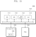
- FIG. 15 illustrates a block diagram of a computing system including a storage device according to embodiments of the inventive concepts.
- a computing system 2000 may include a host device 2100, a storage device 2200, and/or an FPGA 2300.
- a function and a configuration of the host device 2100 may be substantially the same as the function and the configuration of the host device 1100 of FIG. 1 , and thus, additional description will be omitted to avoid redundancy.
- the storage device 2200 may enqueue stream data in a buffer 2260 in the unit of a requested chunk size in response to the streaming access command SA_CMD provided from the outside.
- the streaming read command SR_CMD and the steaming write command SW_CMD may be collectively referred to as the "streaming access command SA_CMD”.
- the storage device 2200 may be storage including solid state drives (SSD), secure digital (SD ® ) cards, or embedded multimedia cards (eMMC ® ).
- a memory region of the buffer 2260 may be mapped onto a virtual memory space of the host 2100 and may be shared by devices constituting the computing system 2000.
- the buffer 2260 may be mapped onto a virtual address corresponding to a streaming window of the virtual memory space.
- the memory region of the buffer 2260 may be shared in such a way that the host 2100, the FPGA 2300, and/or peripheral devices access a streaming window of the virtual memory space.
- the streaming access command SA_CMD may include information such as one or more of an LBA list, a stream ID, a chunk size, a priority, etc.
- the FPGA 2300 is only an example component of a device to process stream data that are exchanged with the storage device 2200.
- the FPGA 2300 may be implemented with various processors, intellectual property (IP), or an ASIC capable of processing stream data.
- the FPGA 2300 may process stream data that the storage device 2200 outputs in response to the streaming access command SA_CMD and may transfer a result value of the processing to the host 2100.
- the storage device 2200 may load stream data onto the buffer 2260 in the unit of a requested data size (chunk size) in response to the streaming read command SR_CMD.
- the FPGA 2300 may receive the stream data loaded onto the buffer 2260 by using a streaming window assigned in the virtual memory space.
- a bandwidth between the host 2100 and the storage device 2200 may not decrease due to a transfer of the stream data. Accordingly, the operation of the FPGA 2300 may make it possible to markedly improve (i.e., minimize) a decrease in a bandwidth due to the exchange of stream data between the storage device 2200 and the host 2100.
- a structure of the computing system 2000 according to embodiments of the inventive concepts is briefly described above.
- the FPGA 2300 that processes a data intensive workload may be positioned outside the storage device 2200.
- the streaming access command SA_CMD may be generated by the host 2100 or the FPGA 2300 or within the storage device 2200.
- the streaming access command SA_CMD may allow the computing system 2000 of the inventive concepts to process stream data efficiently.
- FIG. 16 illustrates a block diagram of an example configuration of a host, a storage device, and an FPGA of FIG. 15 .
- the storage device 2200 and/or the FPGA 2300 may be provided within the computing system 2000 as individual devices.
- the host 2100 may include a central processing unit 2110, a host memory 2150, an interface circuit 2190, and/or a memory management unit 2160 for the purpose of processing stream data.
- the host 2100 may further include components such as a graphics processing unit 2130 and/or a network interface card 2170 such as shown in FIG. 15 .
- the central processing unit 2110, the host memory 2150, and/or the interface circuit 2190 may be substantially the same as those of FIG. 2 , and thus, additional description will be omitted to avoid redundancy.
- a streaming window that may allow a DMA engine 2211 of the FPGA 2300 to access a memory region of the buffer 2260 in the storage device 2200 may be assigned in a virtual memory space of the host 2100.
- the host 2100 may include the memory management unit 2160 for the purpose of managing a streaming window mapped onto the virtual memory space.
- the memory management unit 2160 may register the buffer 2260 of the storage device 2200 at the virtual memory space to provide memory sharing for an input/output of stream data.
- the storage device 2200 may include the storage controller 2220, the nonvolatile memory device 2240 and/or the buffer 2260.
- the storage device 2200 may load data read from the nonvolatile memory device 2240 onto the buffer 2260 in the unit of a chunk size in response to the streaming read command SR_CMD.
- the storage device 2200 may program data read from the buffer 2260 to the nonvolatile memory device 2240 in the unit of a chunk size in response to the steaming write command SW_CMD.
- the buffer 2260 may be mapped onto the virtual memory space of the host 2100, and thus, the buffer 2260 may be accessible by the DMA engine 2211 of the FPGA 2300.
- the FPGA 2300 may include the DMA engine 2211 and/or a kernel memory 2213.
- the FPGA 2300 may be implemented with one or more processor cores, an FPGA, etc.
- the FPGA 2300 may provide the streaming access command SA_CMD of the inventive concepts to the storage device 2200 in response to a request of the host 2100.
- the FPGA 2300 may process stream data transferred from the storage device 2200 and may transfer the processed data to the host 2100.
- the DMA engine 2211 may read stream data of a chunk size loaded onto the buffer 2260 of the storage device 2200 and may transfer the read data to the kernel memory 2213.
Claims (12)
- Système comprenant un dispositif de stockage (1200), un hôte (1100) et des dispositifs périphériques (1110, 1130, 1170), dans lequel le dispositif de stockage (1200) est connecté à l'hôte (1100), qui permet aux dispositifs périphériques (1110, 1130, 1170) d'envoyer des instructions au dispositif de stockage (1200), l'hôte (1100) utilisant une mémoire virtuelle (1161) pour permettre un accès de mémoire direct au dispositif de stockage (1200) pour les dispositifs périphériques (1110, 1130, 1170) enregistrés dans la mémoire virtuelle (1161), le dispositif de stockage (1200) comprenant :un disque statique à semi-conducteurs (1230) comprenant une mémoire non volatile (1233) et un tampon (1235), le disque statique à semi-conducteurs (1230) étant configuré pour recevoir une instruction d'accès à la diffusion en continu (10) incluant une liste (12) d'adresses de blocs logiques, LBA, et une taille de fragment (13) provenant d'un des dispositifs périphériques (1110, 1130, 1170), et pour pré-extraire sur le tampon (1235) des données de flux demandées, provenant de la mémoire non volatile (1233) selon la liste de LBA (12), dans des unités de la taille de fragment (13) sans une instruction supplémentaire ; etun bloc informatique en stockage (1210) configuré pour lire séquentiellement dans le tampon (1235) les données de flux chargées sur le tampon (1235) dans des unités de la taille de fragment (13) incluses dans l'instruction d'accès à la diffusion en continu (10), le bloc informatique en stockage (1210) accédant à une zone de diffusion en continu (1162) enregistrée sur ladite mémoire virtuelle (1161) pour ainsi fournir des résultats de la lecture séquentielle à la mémoire virtuelle (1161) ;dans lequel le tampon (1235) est mappé sur une adresse de mémoire virtuelle de ladite zone de diffusion en continu enregistrée (1162), etdans lequel la taille de fragment (13) est une unité de gestion des données de flux.
- Système selon la revendication 1, comprenant l'hôte (1100), dans lequel le disque statique à semi-conducteurs (1230) est configuré pour mapper une adresse physique du tampon (1235) sur la zone de diffusion en continu (1162) sur la mémoire virtuelle (1161) pendant une opération d'initialisation de l'hôte (1100).
- Système selon la revendication 2, dans lequel le disque statique à semi-conducteurs (1230) est configuré pour communiquer avec l'hôte (1100) conformément à un protocole d'interface PCle ou NVMe, et
dans lequel, pendant l'opération d'initialisation, le disque statique à semi-conducteurs (1230) est configuré pour enregistrer le tampon (1235) au niveau de la zone de diffusion en continu (1162) de la mémoire virtuelle (1161) en réglant un registre d'adresses de base (BAR) de l'hôte (1100). - Système selon une quelconque revendication précédente, dans lequel l'instruction d'accès à la diffusion en continu (10) comprend en outre un identificateur de flux, ID, (11) des données de flux et une priorité (14), etdans lequel la liste de LBA (12) correspond à toutes les adresses logiques des données de flux, etla priorité (14) est attribuée à l'identificateur de flux (11).
- Système selon une quelconque revendication précédente, dans lequel l'instruction d'accès à la diffusion en continu (10) comprend en outre une adresse de destination pour recevoir les données de flux.
- Système selon une quelconque revendication précédente, dans lequel le bloc informatique en stockage (1210) est configuré pour réaliser une opération de balayage de base de données sur les données de flux lues dans les unités de la taille de fragment (13), dans lequel le balayage de base de données sélectionne des données provenant des données de flux.
- Système selon la revendication 6, comprenant l'hôte (1100), dans lequel le bloc informatique en stockage (1210) est en outre configuré pour transférer un résultat de l'opération de balayage de base de données à l'hôte (1100).
- Système selon une quelconque revendication précédente, configuré pour recevoir l'instruction d'accès à la diffusion en continu (10) émise depuis un dit hôte (1100) ou dans lequel le bloc informatique en stockage (1210) est configuré pour émettre l'instruction d'accès à la diffusion en continu (10).
- Système selon une quelconque revendication précédente, pour permettre à l'accès à la zone de diffusion en continu (1162) par le bloc informatique en stockage (1210) d'être redirigé vers le tampon (1235) par un dit hôte (1100).
- Système selon une quelconque revendication précédente, dans lequel la zone de diffusion en continu (1162) comprend une ou plusieurs fenêtres de diffusion en continu (SW1, SW2) qui sont des plages d'adresses virtuelles pour gérer des flux de données respectifs des données de flux dans les unités de la taille de fragment (13).
- Système selon la revendication 10, dans lequel l'instruction d'accès à la diffusion en continu (10) comprend en outre un identificateur de flux (ID) des données de flux, et
dans lequel un nombre des fenêtres de diffusion en continu (SW1, SW2) attribuées correspond à un nombre d'identificateurs de flux attribués au disque statique à semi-conducteurs (1230). - Procédé de fonctionnement d'un dispositif de stockage (1200) qui est connecté à un hôte (1100) qui utilise un espace de mémoire virtuelle (1161) pour permettre un accès de mémoire direct au dispositif de stockage (1200) pour des dispositifs cibles (1110, 1130, 1170) enregistrés dans la mémoire virtuelle (1161), et qui inclut une mémoire non volatile (1233) et un tampon (1235), le procédé comprenant :le mappage, par le dispositif de stockage (1200), d'une adresse physique du tampon (1235) sur une plage d'adresses correspondant à une fenêtre de diffusion en continu (SW1, SW2) de l'espace de mémoire virtuelle (1161) ;la réception, au niveau du dispositif de stockage (1200), d'une instruction d'accès à la diffusion en continu (10) incluant une liste de LBA (12) correspondant à des données de flux et une taille de fragment (13) des données de flux provenant d'un des dispositifs cibles (1110, 1130, 1170) ;la pré-extraction sur le tampon (1235), par le dispositif de stockage (1200), des données de flux séquentiellement dans des unités de la taille de fragment (13) provenant de la mémoire non volatile (1233) avec référence à la liste de LBA (12) ;l'accès, par un des dispositifs cibles (1110, 1130, 1170), à la fenêtre de diffusion en continu (SW1, SW2) de l'espace de mémoire virtuelle (1161) ;la redirection, au niveau du dispositif hôte (1100), de l'accès à la fenêtre de diffusion en continu (SW1, SW2) vers le tampon (1235) ; etle transfert, au niveau du dispositif hôte (1100), des données de flux chargées séquentiellement sur le tampon (1235) à un des dispositifs cibles (1110, 1130, 1170), dans des unités de la taille de fragment (13),dans lequel la taille de fragment (13) est une unité de gestion des données de flux.
Applications Claiming Priority (2)
| Application Number | Priority Date | Filing Date | Title |
|---|---|---|---|
| KR20180133653 | 2018-11-02 | ||
| KR1020190027103A KR20200051450A (ko) | 2018-11-02 | 2019-03-08 | 스트림 데이터를 처리하는 스토리지 장치, 그것의 포함하는 컴퓨팅 시스템, 그리고 그것의 동작 방법 |
Publications (2)
| Publication Number | Publication Date |
|---|---|
| EP3647932A1 EP3647932A1 (fr) | 2020-05-06 |
| EP3647932B1 true EP3647932B1 (fr) | 2023-06-28 |
Family
ID=68387145
Family Applications (1)
| Application Number | Title | Priority Date | Filing Date |
|---|---|---|---|
| EP19205624.0A Active EP3647932B1 (fr) | 2018-11-02 | 2019-10-28 | Dispositif de stockage de traitement de données de flux, système le comprenant et son procédé de fonctionnement |
Country Status (3)
| Country | Link |
|---|---|
| US (2) | US11061591B2 (fr) |
| EP (1) | EP3647932B1 (fr) |
| CN (1) | CN111143234A (fr) |
Families Citing this family (7)
| Publication number | Priority date | Publication date | Assignee | Title |
|---|---|---|---|---|
| US20220345414A1 (en) * | 2019-08-30 | 2022-10-27 | Unitex Corporation | Interface Conversion Device |
| US11422921B2 (en) * | 2019-12-31 | 2022-08-23 | Western Digital Technologies, Inc. | Debug systems for deterministic validation of data storage devices |
| CN114598660A (zh) * | 2020-12-04 | 2022-06-07 | 大唐移动通信设备有限公司 | 传输窗口的调整方法、装置、发送设备、接收设备及介质 |
| CN114626541A (zh) * | 2020-12-11 | 2022-06-14 | 上海阵量智能科技有限公司 | 命令下发方法、装置、处理设备、计算机设备及存储介质 |
| JP2023027970A (ja) * | 2021-08-18 | 2023-03-03 | キオクシア株式会社 | メモリシステム |
| US11733927B2 (en) * | 2021-11-30 | 2023-08-22 | Microsoft Technology Licensing, Llc | Hybrid solid-state drive |
| US20230185739A1 (en) * | 2021-12-10 | 2023-06-15 | Samsung Electronics Co., Ltd. | Efficient and concurrent model execution |
Family Cites Families (24)
| Publication number | Priority date | Publication date | Assignee | Title |
|---|---|---|---|---|
| JPH1060506A (ja) | 1996-08-14 | 1998-03-03 | Sumitomo Metal Ind Ltd | 高炉操業方法 |
| JP4060506B2 (ja) | 1999-12-28 | 2008-03-12 | 株式会社東芝 | ディスク制御装置 |
| US6799264B2 (en) | 2001-02-20 | 2004-09-28 | Koninklijke Philips Electronics N.V. | Memory accelerator for ARM processor pre-fetching multiple instructions from cyclically sequential memory partitions |
| US6760818B2 (en) | 2002-05-01 | 2004-07-06 | Koninklijke Philips Electronics N.V. | Memory region based data pre-fetching |
| WO2003104943A2 (fr) | 2002-06-11 | 2003-12-18 | Ashish A Pandya | Processeur ip a performance elevee pour des applications de stockage tcp/ip, rdma et ip |
| KR100881748B1 (ko) | 2002-12-30 | 2009-02-06 | 주식회사 하이닉스반도체 | 고속으로 데이터를 출력하기 위한 메모리 장치 |
| US7493450B2 (en) * | 2003-04-14 | 2009-02-17 | Hewlett-Packard Development Company, L.P. | Method of triggering read cache pre-fetch to increase host read throughput |
| US7194582B1 (en) * | 2003-05-30 | 2007-03-20 | Mips Technologies, Inc. | Microprocessor with improved data stream prefetching |
| US7177985B1 (en) * | 2003-05-30 | 2007-02-13 | Mips Technologies, Inc. | Microprocessor with improved data stream prefetching |
| JP4862566B2 (ja) | 2006-09-04 | 2012-01-25 | 富士通株式会社 | 動画像処理装置及びプリフェッチ制御方法 |
| US8719455B2 (en) | 2010-06-28 | 2014-05-06 | International Business Machines Corporation | DMA-based acceleration of command push buffer between host and target devices |
| TWI430104B (zh) * | 2011-07-04 | 2014-03-11 | Phison Electronics Corp | 資料串分派與傳送方法、記憶體控制器與記憶體儲存裝置 |
| US9817761B2 (en) | 2012-01-06 | 2017-11-14 | Sandisk Technologies Llc | Methods, systems, and computer readable media for optimization of host sequential reads or writes based on volume of data transfer |
| KR102074329B1 (ko) | 2013-09-06 | 2020-02-06 | 삼성전자주식회사 | 데이터 저장 장치 및 그것의 데이터 처리 방법 |
| US20170228173A9 (en) * | 2014-05-02 | 2017-08-10 | Cavium, Inc. | Systems and methods for enabling local caching for remote storage devices over a network via nvme controller |
| US10031857B2 (en) | 2014-05-27 | 2018-07-24 | Mellanox Technologies, Ltd. | Address translation services for direct accessing of local memory over a network fabric |
| EP3049915B1 (fr) | 2014-12-14 | 2020-02-12 | VIA Alliance Semiconductor Co., Ltd. | Préextraction avec niveau d'agressivité en fonction de l'efficacité par type d'accès à la mémoire |
| US9760281B2 (en) | 2015-03-27 | 2017-09-12 | Intel Corporation | Sequential write stream management |
| US10656838B2 (en) * | 2015-07-13 | 2020-05-19 | Samsung Electronics Co., Ltd. | Automatic stream detection and assignment algorithm |
| JP1566737S (fr) | 2015-10-12 | 2017-01-10 | ||
| US9977623B2 (en) * | 2015-10-15 | 2018-05-22 | Sandisk Technologies Llc | Detection of a sequential command stream |
| US9916269B1 (en) | 2016-04-14 | 2018-03-13 | Amazon Technologies, Inc. | Packet queueing for network device |
| US10417140B2 (en) * | 2017-02-24 | 2019-09-17 | Advanced Micro Devices, Inc. | Streaming translation lookaside buffer |
| US10564853B2 (en) * | 2017-04-26 | 2020-02-18 | Western Digital Technologies, Inc. | System and method for locality detection to identify read or write streams in a memory device |
-
2019
- 2019-09-05 US US16/562,094 patent/US11061591B2/en active Active
- 2019-10-28 EP EP19205624.0A patent/EP3647932B1/fr active Active
- 2019-11-01 CN CN201911064637.6A patent/CN111143234A/zh active Pending
-
2021
- 2021-06-10 US US17/344,112 patent/US11635902B2/en active Active
Also Published As
| Publication number | Publication date |
|---|---|
| EP3647932A1 (fr) | 2020-05-06 |
| CN111143234A (zh) | 2020-05-12 |
| US11635902B2 (en) | 2023-04-25 |
| US20210303189A1 (en) | 2021-09-30 |
| US20200142621A1 (en) | 2020-05-07 |
| US11061591B2 (en) | 2021-07-13 |
Similar Documents
| Publication | Publication Date | Title |
|---|---|---|
| EP3647932B1 (fr) | Dispositif de stockage de traitement de données de flux, système le comprenant et son procédé de fonctionnement | |
| US9785545B2 (en) | Method and apparatus for providing dual memory access to non-volatile memory | |
| US10896136B2 (en) | Storage system including secondary memory that predicts and prefetches data | |
| EP2849076B1 (fr) | Procédé et système de transmission dma | |
| US10970003B2 (en) | Scalable low-latency storage interface | |
| KR101841997B1 (ko) | 순응적 존속을 위한 시스템, 방법 및 인터페이스 | |
| US9395921B2 (en) | Writing data using DMA by specifying a buffer address and a flash memory address | |
| US10114589B2 (en) | Command control for multi-core non-volatile memory | |
| US8683126B2 (en) | Optimal use of buffer space by a storage controller which writes retrieved data directly to a memory | |
| US20150169244A1 (en) | Storage processor managing nvme logically addressed solid state disk array | |
| US11379374B2 (en) | Systems and methods for streaming storage device content | |
| US20180074757A1 (en) | Switch and memory device | |
| US9098209B2 (en) | Communication via a memory interface | |
| TWI696188B (zh) | 混合式記憶體系統 | |
| CN110275840B (zh) | 在存储器接口上的分布式过程执行和文件系统 | |
| EP4220419B1 (fr) | Modification de pointeurs de liste de pages de région physique nvme et de pointeurs de données pour faciliter le routage de demandes de mémoire pcie | |
| EP3270293B1 (fr) | Tampons de commande à deux étages pour recouvrir une carte iommu et des secondes lectures de mémoires d'architecture multiniveaux | |
| US10564847B1 (en) | Data movement bulk copy operation | |
| KR20200051450A (ko) | 스트림 데이터를 처리하는 스토리지 장치, 그것의 포함하는 컴퓨팅 시스템, 그리고 그것의 동작 방법 | |
| KR20220050177A (ko) | 3단의 계층적 메모리 시스템 | |
| CN112703481A (zh) | 混合式存储器系统接口 |
Legal Events
| Date | Code | Title | Description |
|---|---|---|---|
| PUAI | Public reference made under article 153(3) epc to a published international application that has entered the european phase |
Free format text: ORIGINAL CODE: 0009012 |
|
| STAA | Information on the status of an ep patent application or granted ep patent |
Free format text: STATUS: THE APPLICATION HAS BEEN PUBLISHED |
|
| AK | Designated contracting states |
Kind code of ref document: A1 Designated state(s): AL AT BE BG CH CY CZ DE DK EE ES FI FR GB GR HR HU IE IS IT LI LT LU LV MC MK MT NL NO PL PT RO RS SE SI SK SM TR |
|
| AX | Request for extension of the european patent |
Extension state: BA ME |
|
| STAA | Information on the status of an ep patent application or granted ep patent |
Free format text: STATUS: REQUEST FOR EXAMINATION WAS MADE |
|
| 17P | Request for examination filed |
Effective date: 20200928 |
|
| RBV | Designated contracting states (corrected) |
Designated state(s): AL AT BE BG CH CY CZ DE DK EE ES FI FR GB GR HR HU IE IS IT LI LT LU LV MC MK MT NL NO PL PT RO RS SE SI SK SM TR |
|
| STAA | Information on the status of an ep patent application or granted ep patent |
Free format text: STATUS: EXAMINATION IS IN PROGRESS |
|
| 17Q | First examination report despatched |
Effective date: 20211005 |
|
| GRAP | Despatch of communication of intention to grant a patent |
Free format text: ORIGINAL CODE: EPIDOSNIGR1 |
|
| STAA | Information on the status of an ep patent application or granted ep patent |
Free format text: STATUS: GRANT OF PATENT IS INTENDED |
|
| RIC1 | Information provided on ipc code assigned before grant |
Ipc: G06F 12/0862 20160101ALI20221216BHEP Ipc: G06F 12/02 20060101ALI20221216BHEP Ipc: G06F 12/109 20160101ALI20221216BHEP Ipc: G06F 12/1081 20160101ALI20221216BHEP Ipc: G06F 3/06 20060101AFI20221216BHEP |
|
| INTG | Intention to grant announced |
Effective date: 20230111 |
|
| GRAS | Grant fee paid |
Free format text: ORIGINAL CODE: EPIDOSNIGR3 |
|
| GRAA | (expected) grant |
Free format text: ORIGINAL CODE: 0009210 |
|
| STAA | Information on the status of an ep patent application or granted ep patent |
Free format text: STATUS: THE PATENT HAS BEEN GRANTED |
|
| AK | Designated contracting states |
Kind code of ref document: B1 Designated state(s): AL AT BE BG CH CY CZ DE DK EE ES FI FR GB GR HR HU IE IS IT LI LT LU LV MC MK MT NL NO PL PT RO RS SE SI SK SM TR |
|
| P01 | Opt-out of the competence of the unified patent court (upc) registered |
Effective date: 20230520 |
|
| REG | Reference to a national code |
Ref country code: CH Ref legal event code: EP |
|
| REG | Reference to a national code |
Ref country code: AT Ref legal event code: REF Ref document number: 1583294 Country of ref document: AT Kind code of ref document: T Effective date: 20230715 |
|
| REG | Reference to a national code |
Ref country code: IE Ref legal event code: FG4D |
|
| REG | Reference to a national code |
Ref country code: DE Ref legal event code: R096 Ref document number: 602019031624 Country of ref document: DE |
|
| REG | Reference to a national code |
Ref country code: LT Ref legal event code: MG9D |
|
| PG25 | Lapsed in a contracting state [announced via postgrant information from national office to epo] |
Ref country code: SE Free format text: LAPSE BECAUSE OF FAILURE TO SUBMIT A TRANSLATION OF THE DESCRIPTION OR TO PAY THE FEE WITHIN THE PRESCRIBED TIME-LIMIT Effective date: 20230628 Ref country code: NO Free format text: LAPSE BECAUSE OF FAILURE TO SUBMIT A TRANSLATION OF THE DESCRIPTION OR TO PAY THE FEE WITHIN THE PRESCRIBED TIME-LIMIT Effective date: 20230928 |
|
| PGFP | Annual fee paid to national office [announced via postgrant information from national office to epo] |
Ref country code: GB Payment date: 20230907 Year of fee payment: 5 |
|
| REG | Reference to a national code |
Ref country code: NL Ref legal event code: MP Effective date: 20230628 |
|
| REG | Reference to a national code |
Ref country code: AT Ref legal event code: MK05 Ref document number: 1583294 Country of ref document: AT Kind code of ref document: T Effective date: 20230628 |
|
| PG25 | Lapsed in a contracting state [announced via postgrant information from national office to epo] |
Ref country code: RS Free format text: LAPSE BECAUSE OF FAILURE TO SUBMIT A TRANSLATION OF THE DESCRIPTION OR TO PAY THE FEE WITHIN THE PRESCRIBED TIME-LIMIT Effective date: 20230628 Ref country code: NL Free format text: LAPSE BECAUSE OF FAILURE TO SUBMIT A TRANSLATION OF THE DESCRIPTION OR TO PAY THE FEE WITHIN THE PRESCRIBED TIME-LIMIT Effective date: 20230628 Ref country code: LV Free format text: LAPSE BECAUSE OF FAILURE TO SUBMIT A TRANSLATION OF THE DESCRIPTION OR TO PAY THE FEE WITHIN THE PRESCRIBED TIME-LIMIT Effective date: 20230628 Ref country code: LT Free format text: LAPSE BECAUSE OF FAILURE TO SUBMIT A TRANSLATION OF THE DESCRIPTION OR TO PAY THE FEE WITHIN THE PRESCRIBED TIME-LIMIT Effective date: 20230628 Ref country code: HR Free format text: LAPSE BECAUSE OF FAILURE TO SUBMIT A TRANSLATION OF THE DESCRIPTION OR TO PAY THE FEE WITHIN THE PRESCRIBED TIME-LIMIT Effective date: 20230628 Ref country code: GR Free format text: LAPSE BECAUSE OF FAILURE TO SUBMIT A TRANSLATION OF THE DESCRIPTION OR TO PAY THE FEE WITHIN THE PRESCRIBED TIME-LIMIT Effective date: 20230929 |
|
| PGFP | Annual fee paid to national office [announced via postgrant information from national office to epo] |
Ref country code: BE Payment date: 20230918 Year of fee payment: 5 |
|
| PG25 | Lapsed in a contracting state [announced via postgrant information from national office to epo] |
Ref country code: FI Free format text: LAPSE BECAUSE OF FAILURE TO SUBMIT A TRANSLATION OF THE DESCRIPTION OR TO PAY THE FEE WITHIN THE PRESCRIBED TIME-LIMIT Effective date: 20230628 |
|
| PG25 | Lapsed in a contracting state [announced via postgrant information from national office to epo] |
Ref country code: SK Free format text: LAPSE BECAUSE OF FAILURE TO SUBMIT A TRANSLATION OF THE DESCRIPTION OR TO PAY THE FEE WITHIN THE PRESCRIBED TIME-LIMIT Effective date: 20230628 |
|
| PG25 | Lapsed in a contracting state [announced via postgrant information from national office to epo] |
Ref country code: ES Free format text: LAPSE BECAUSE OF FAILURE TO SUBMIT A TRANSLATION OF THE DESCRIPTION OR TO PAY THE FEE WITHIN THE PRESCRIBED TIME-LIMIT Effective date: 20230628 |
|
| PG25 | Lapsed in a contracting state [announced via postgrant information from national office to epo] |
Ref country code: IS Free format text: LAPSE BECAUSE OF FAILURE TO SUBMIT A TRANSLATION OF THE DESCRIPTION OR TO PAY THE FEE WITHIN THE PRESCRIBED TIME-LIMIT Effective date: 20231028 |
|
| PG25 | Lapsed in a contracting state [announced via postgrant information from national office to epo] |
Ref country code: SM Free format text: LAPSE BECAUSE OF FAILURE TO SUBMIT A TRANSLATION OF THE DESCRIPTION OR TO PAY THE FEE WITHIN THE PRESCRIBED TIME-LIMIT Effective date: 20230628 Ref country code: SK Free format text: LAPSE BECAUSE OF FAILURE TO SUBMIT A TRANSLATION OF THE DESCRIPTION OR TO PAY THE FEE WITHIN THE PRESCRIBED TIME-LIMIT Effective date: 20230628 Ref country code: RO Free format text: LAPSE BECAUSE OF FAILURE TO SUBMIT A TRANSLATION OF THE DESCRIPTION OR TO PAY THE FEE WITHIN THE PRESCRIBED TIME-LIMIT Effective date: 20230628 Ref country code: PT Free format text: LAPSE BECAUSE OF FAILURE TO SUBMIT A TRANSLATION OF THE DESCRIPTION OR TO PAY THE FEE WITHIN THE PRESCRIBED TIME-LIMIT Effective date: 20231030 Ref country code: IS Free format text: LAPSE BECAUSE OF FAILURE TO SUBMIT A TRANSLATION OF THE DESCRIPTION OR TO PAY THE FEE WITHIN THE PRESCRIBED TIME-LIMIT Effective date: 20231028 Ref country code: ES Free format text: LAPSE BECAUSE OF FAILURE TO SUBMIT A TRANSLATION OF THE DESCRIPTION OR TO PAY THE FEE WITHIN THE PRESCRIBED TIME-LIMIT Effective date: 20230628 Ref country code: EE Free format text: LAPSE BECAUSE OF FAILURE TO SUBMIT A TRANSLATION OF THE DESCRIPTION OR TO PAY THE FEE WITHIN THE PRESCRIBED TIME-LIMIT Effective date: 20230628 Ref country code: CZ Free format text: LAPSE BECAUSE OF FAILURE TO SUBMIT A TRANSLATION OF THE DESCRIPTION OR TO PAY THE FEE WITHIN THE PRESCRIBED TIME-LIMIT Effective date: 20230628 Ref country code: AT Free format text: LAPSE BECAUSE OF FAILURE TO SUBMIT A TRANSLATION OF THE DESCRIPTION OR TO PAY THE FEE WITHIN THE PRESCRIBED TIME-LIMIT Effective date: 20230628 |
|
| PGFP | Annual fee paid to national office [announced via postgrant information from national office to epo] |
Ref country code: DE Payment date: 20230906 Year of fee payment: 5 |
|
| PG25 | Lapsed in a contracting state [announced via postgrant information from national office to epo] |
Ref country code: PL Free format text: LAPSE BECAUSE OF FAILURE TO SUBMIT A TRANSLATION OF THE DESCRIPTION OR TO PAY THE FEE WITHIN THE PRESCRIBED TIME-LIMIT Effective date: 20230628 |