EP3644384A1 - Deep homo (highest occupied molecular orbital) emitter device structures - Google Patents
Deep homo (highest occupied molecular orbital) emitter device structures Download PDFInfo
- Publication number
- EP3644384A1 EP3644384A1 EP19204284.4A EP19204284A EP3644384A1 EP 3644384 A1 EP3644384 A1 EP 3644384A1 EP 19204284 A EP19204284 A EP 19204284A EP 3644384 A1 EP3644384 A1 EP 3644384A1
- Authority
- EP
- European Patent Office
- Prior art keywords
- compound
- homo
- oled
- formula
- group
- Prior art date
- Legal status (The legal status is an assumption and is not a legal conclusion. Google has not performed a legal analysis and makes no representation as to the accuracy of the status listed.)
- Pending
Links
- 0 Cc(cccc1)c1-c1ccccc1* Chemical compound Cc(cccc1)c1-c1ccccc1* 0.000 description 27
- HYQBWCRBGGYLTL-UHFFFAOYSA-N CC(CO)(C(C)(C=C)N(C)C=N)c1c(C)cc(C)cc1 Chemical compound CC(CO)(C(C)(C=C)N(C)C=N)c1c(C)cc(C)cc1 HYQBWCRBGGYLTL-UHFFFAOYSA-N 0.000 description 1
Images


Classifications
-
- H—ELECTRICITY
- H10—SEMICONDUCTOR DEVICES; ELECTRIC SOLID-STATE DEVICES NOT OTHERWISE PROVIDED FOR
- H10K—ORGANIC ELECTRIC SOLID-STATE DEVICES
- H10K50/00—Organic light-emitting devices
- H10K50/10—OLEDs or polymer light-emitting diodes [PLED]
- H10K50/11—OLEDs or polymer light-emitting diodes [PLED] characterised by the electroluminescent [EL] layers
- H10K50/12—OLEDs or polymer light-emitting diodes [PLED] characterised by the electroluminescent [EL] layers comprising dopants
-
- H—ELECTRICITY
- H10—SEMICONDUCTOR DEVICES; ELECTRIC SOLID-STATE DEVICES NOT OTHERWISE PROVIDED FOR
- H10K—ORGANIC ELECTRIC SOLID-STATE DEVICES
- H10K50/00—Organic light-emitting devices
- H10K50/10—OLEDs or polymer light-emitting diodes [PLED]
- H10K50/11—OLEDs or polymer light-emitting diodes [PLED] characterised by the electroluminescent [EL] layers
-
- C—CHEMISTRY; METALLURGY
- C09—DYES; PAINTS; POLISHES; NATURAL RESINS; ADHESIVES; COMPOSITIONS NOT OTHERWISE PROVIDED FOR; APPLICATIONS OF MATERIALS NOT OTHERWISE PROVIDED FOR
- C09K—MATERIALS FOR MISCELLANEOUS APPLICATIONS, NOT PROVIDED FOR ELSEWHERE
- C09K11/00—Luminescent materials, e.g. electroluminescent or chemiluminescent
- C09K11/06—Luminescent materials, e.g. electroluminescent or chemiluminescent containing organic luminescent materials
-
- H—ELECTRICITY
- H10—SEMICONDUCTOR DEVICES; ELECTRIC SOLID-STATE DEVICES NOT OTHERWISE PROVIDED FOR
- H10K—ORGANIC ELECTRIC SOLID-STATE DEVICES
- H10K50/00—Organic light-emitting devices
- H10K50/10—OLEDs or polymer light-emitting diodes [PLED]
-
- H—ELECTRICITY
- H10—SEMICONDUCTOR DEVICES; ELECTRIC SOLID-STATE DEVICES NOT OTHERWISE PROVIDED FOR
- H10K—ORGANIC ELECTRIC SOLID-STATE DEVICES
- H10K50/00—Organic light-emitting devices
- H10K50/10—OLEDs or polymer light-emitting diodes [PLED]
- H10K50/18—Carrier blocking layers
-
- H—ELECTRICITY
- H10—SEMICONDUCTOR DEVICES; ELECTRIC SOLID-STATE DEVICES NOT OTHERWISE PROVIDED FOR
- H10K—ORGANIC ELECTRIC SOLID-STATE DEVICES
- H10K50/00—Organic light-emitting devices
- H10K50/80—Constructional details
- H10K50/805—Electrodes
- H10K50/81—Anodes
-
- H—ELECTRICITY
- H10—SEMICONDUCTOR DEVICES; ELECTRIC SOLID-STATE DEVICES NOT OTHERWISE PROVIDED FOR
- H10K—ORGANIC ELECTRIC SOLID-STATE DEVICES
- H10K50/00—Organic light-emitting devices
- H10K50/80—Constructional details
- H10K50/805—Electrodes
- H10K50/82—Cathodes
-
- H—ELECTRICITY
- H10—SEMICONDUCTOR DEVICES; ELECTRIC SOLID-STATE DEVICES NOT OTHERWISE PROVIDED FOR
- H10K—ORGANIC ELECTRIC SOLID-STATE DEVICES
- H10K59/00—Integrated devices, or assemblies of multiple devices, comprising at least one organic light-emitting element covered by group H10K50/00
- H10K59/90—Assemblies of multiple devices comprising at least one organic light-emitting element
-
- H—ELECTRICITY
- H10—SEMICONDUCTOR DEVICES; ELECTRIC SOLID-STATE DEVICES NOT OTHERWISE PROVIDED FOR
- H10K—ORGANIC ELECTRIC SOLID-STATE DEVICES
- H10K85/00—Organic materials used in the body or electrodes of devices covered by this subclass
- H10K85/30—Coordination compounds
- H10K85/341—Transition metal complexes, e.g. Ru(II)polypyridine complexes
- H10K85/342—Transition metal complexes, e.g. Ru(II)polypyridine complexes comprising iridium
-
- H—ELECTRICITY
- H10—SEMICONDUCTOR DEVICES; ELECTRIC SOLID-STATE DEVICES NOT OTHERWISE PROVIDED FOR
- H10K—ORGANIC ELECTRIC SOLID-STATE DEVICES
- H10K85/00—Organic materials used in the body or electrodes of devices covered by this subclass
- H10K85/60—Organic compounds having low molecular weight
- H10K85/649—Aromatic compounds comprising a hetero atom
- H10K85/654—Aromatic compounds comprising a hetero atom comprising only nitrogen as heteroatom
-
- H—ELECTRICITY
- H10—SEMICONDUCTOR DEVICES; ELECTRIC SOLID-STATE DEVICES NOT OTHERWISE PROVIDED FOR
- H10K—ORGANIC ELECTRIC SOLID-STATE DEVICES
- H10K85/00—Organic materials used in the body or electrodes of devices covered by this subclass
- H10K85/60—Organic compounds having low molecular weight
- H10K85/649—Aromatic compounds comprising a hetero atom
- H10K85/657—Polycyclic condensed heteroaromatic hydrocarbons
- H10K85/6572—Polycyclic condensed heteroaromatic hydrocarbons comprising only nitrogen in the heteroaromatic polycondensed ring system, e.g. phenanthroline or carbazole
-
- H—ELECTRICITY
- H10—SEMICONDUCTOR DEVICES; ELECTRIC SOLID-STATE DEVICES NOT OTHERWISE PROVIDED FOR
- H10K—ORGANIC ELECTRIC SOLID-STATE DEVICES
- H10K85/00—Organic materials used in the body or electrodes of devices covered by this subclass
- H10K85/60—Organic compounds having low molecular weight
- H10K85/649—Aromatic compounds comprising a hetero atom
- H10K85/657—Polycyclic condensed heteroaromatic hydrocarbons
- H10K85/6574—Polycyclic condensed heteroaromatic hydrocarbons comprising only oxygen in the heteroaromatic polycondensed ring system, e.g. cumarine dyes
-
- H—ELECTRICITY
- H10—SEMICONDUCTOR DEVICES; ELECTRIC SOLID-STATE DEVICES NOT OTHERWISE PROVIDED FOR
- H10K—ORGANIC ELECTRIC SOLID-STATE DEVICES
- H10K85/00—Organic materials used in the body or electrodes of devices covered by this subclass
- H10K85/60—Organic compounds having low molecular weight
- H10K85/649—Aromatic compounds comprising a hetero atom
- H10K85/657—Polycyclic condensed heteroaromatic hydrocarbons
- H10K85/6576—Polycyclic condensed heteroaromatic hydrocarbons comprising only sulfur in the heteroaromatic polycondensed ring system, e.g. benzothiophene
-
- C—CHEMISTRY; METALLURGY
- C09—DYES; PAINTS; POLISHES; NATURAL RESINS; ADHESIVES; COMPOSITIONS NOT OTHERWISE PROVIDED FOR; APPLICATIONS OF MATERIALS NOT OTHERWISE PROVIDED FOR
- C09K—MATERIALS FOR MISCELLANEOUS APPLICATIONS, NOT PROVIDED FOR ELSEWHERE
- C09K2211/00—Chemical nature of organic luminescent or tenebrescent compounds
- C09K2211/18—Metal complexes
- C09K2211/185—Metal complexes of the platinum group, i.e. Os, Ir, Pt, Ru, Rh or Pd
-
- H—ELECTRICITY
- H10—SEMICONDUCTOR DEVICES; ELECTRIC SOLID-STATE DEVICES NOT OTHERWISE PROVIDED FOR
- H10K—ORGANIC ELECTRIC SOLID-STATE DEVICES
- H10K2101/00—Properties of the organic materials covered by group H10K85/00
- H10K2101/30—Highest occupied molecular orbital [HOMO], lowest unoccupied molecular orbital [LUMO] or Fermi energy values
-
- H—ELECTRICITY
- H10—SEMICONDUCTOR DEVICES; ELECTRIC SOLID-STATE DEVICES NOT OTHERWISE PROVIDED FOR
- H10K—ORGANIC ELECTRIC SOLID-STATE DEVICES
- H10K2101/00—Properties of the organic materials covered by group H10K85/00
- H10K2101/40—Interrelation of parameters between multiple constituent active layers or sublayers, e.g. HOMO values in adjacent layers
-
- H—ELECTRICITY
- H10—SEMICONDUCTOR DEVICES; ELECTRIC SOLID-STATE DEVICES NOT OTHERWISE PROVIDED FOR
- H10K—ORGANIC ELECTRIC SOLID-STATE DEVICES
- H10K2101/00—Properties of the organic materials covered by group H10K85/00
- H10K2101/90—Multiple hosts in the emissive layer
-
- H—ELECTRICITY
- H10—SEMICONDUCTOR DEVICES; ELECTRIC SOLID-STATE DEVICES NOT OTHERWISE PROVIDED FOR
- H10K—ORGANIC ELECTRIC SOLID-STATE DEVICES
- H10K85/00—Organic materials used in the body or electrodes of devices covered by this subclass
- H10K85/60—Organic compounds having low molecular weight
- H10K85/649—Aromatic compounds comprising a hetero atom
- H10K85/657—Polycyclic condensed heteroaromatic hydrocarbons
Definitions
- the present invention relates to compounds for use as emitters, and devices, such as organic light emitting diodes, including the same.
- Opto-electronic devices that make use of organic materials are becoming increasingly desirable for a number of reasons. Many of the materials used to make such devices are relatively inexpensive, so organic opto-electronic devices have the potential for cost advantages over inorganic devices. In addition, the inherent properties of organic materials, such as their flexibility, may make them well suited for particular applications such as fabrication on a flexible substrate. Examples of organic opto-electronic devices include organic light emitting diodes/devices (OLEDs), organic phototransistors, organic photovoltaic cells, and organic photodetectors. For OLEDs, the organic materials may have performance advantages over conventional materials. For example, the wavelength at which an organic emissive layer emits light may generally be readily tuned with appropriate dopants.
- OLEDs make use of thin organic films that emit light when voltage is applied across the device. OLEDs are becoming an increasingly interesting technology for use in applications such as flat panel displays, illumination, and backlighting. Several OLED materials and configurations are described in U.S. Pat. Nos. 5,844,363 , 6,303,238 , and 5,707,745 , which are incorporated herein by reference in their entirety.
- phosphorescent emissive molecules are full color display. Industry standards for such a display call for pixels adapted to emit particular colors, referred to as "saturated" colors. In particular, these standards call for saturated red, green, and blue pixels.
- the OLED can be designed to emit white light. In conventional liquid crystal displays emission from a white backlight is filtered using absorption filters to produce red, green and blue emission. The same technique can also be used with OLEDs.
- the white OLED can be either a single EML device or a stack structure. Color may be measured using CIE coordinates, which are well known to the art.
- organic includes polymeric materials as well as small molecule organic materials that may be used to fabricate organic opto-electronic devices.
- Small molecule refers to any organic material that is not a polymer, and "small molecules” may actually be quite large. Small molecules may include repeat units in some circumstances. For example, using a long chain alkyl group as a substituent does not remove a molecule from the "small molecule” class. Small molecules may also be incorporated into polymers, for example as a pendent group on a polymer backbone or as a part of the backbone. Small molecules may also serve as the core moiety of a dendrimer, which consists of a series of chemical shells built on the core moiety.
- the core moiety of a dendrimer may be a fluorescent or phosphorescent small molecule emitter.
- a dendrimer may be a "small molecule,” and it is believed that all dendrimers currently used in the field of OLEDs are small molecules.
- top means furthest away from the substrate, while “bottom” means closest to the substrate.
- first layer is described as “disposed over” a second layer, the first layer is disposed further away from substrate. There may be other layers between the first and second layer, unless it is specified that the first layer is "in contact with” the second layer.
- a cathode may be described as “disposed over” an anode, even though there are various organic layers in between.
- a ligand may be referred to as "photoactive” when it is believed that the ligand directly contributes to the photoactive properties of an emissive material.
- a ligand may be referred to as "ancillary” when it is believed that the ligand does not contribute to the photoactive properties of an emissive material, although an ancillary ligand may alter the properties of a photoactive ligand.
- a first "Highest Occupied Molecular Orbital” (HOMO) or “Lowest Unoccupied Molecular Orbital” (LUMO) energy level is “greater than” or "higher than” a second HOMO or LUMO energy level if the first energy level is closer to the vacuum energy level.
- IP ionization potentials
- a higher HOMO energy level corresponds to an IP having a smaller absolute value (an IP that is less negative).
- a higher LUMO energy level corresponds to an electron affinity (EA) having a smaller absolute value (an EA that is less negative).
- the LUMO energy level of a material is higher than the HOMO energy level of the same material.
- a "higher” HOMO or LUMO energy level appears closer to the top of such a diagram than a "lower” HOMO or LUMO energy level.
- a first work function is "greater than” or “higher than” a second work function if the first work function has a higher absolute value. Because work functions are generally measured as negative numbers relative to vacuum level, this means that a "higher” work function is more negative. On a conventional energy level diagram, with the vacuum level at the top, a “higher” work function is illustrated as further away from the vacuum level in the downward direction. Thus, the definitions of HOMO and LUMO energy levels follow a different convention than work functions.
- an organic light emitting diode/device is also provided.
- the OLED can include an anode, a cathode, and an organic layer, disposed between the anode and the cathode.
- the organic light emitting device is incorporated into one or more device selected from a consumer product, an electronic component module, and/or a lighting panel.
- An embodiment of the disclosed subject matter may provide an organic light emitting diode (OLED) having an anode, a cathode, an emissive layer disposed between the anode and the cathode, and a hole blocking layer disposed between the emissive and the cathode.
- the emissive layer may include a phosphorescent dopant.
- the phosphorescent dopant may have an emission in 0.5% doped PMMA (Poly(methyl methacrylate)) thin film with a peak maximum wavelength that is greater than or equal to 600 nm at room temperature.
- the energy of a highest occupied molecular orbital (HOMO) of the phosphorescent dopant may be lower than or equal to -5.1 eV, and the energy of the HOMO of the hole blocking layer may be at least 0.1 eV lower than the energy of the HOMO of the phosphorescent dopant.
- HOMO highest occupied molecular orbital
- the peak maximum wavelength of the phosphorescent dopant may be greater than or equal to 610 nm, greater than or equal to 620 nm, greater than or equal to 630 nm, greater than or equal to 650 nm, greater than or equal to 700 nm, greater than or equal to 750 nm, or greater than or equal to 800 nm.
- the OLED may have the hole blocking layer disposed on the emissive layer.
- the energy of the HOMO of the phosphorescent dopant may be lower than or equal to -5.2 eV, lower than or equal to -5.3 eV, or lower than or equal to -5.4 eV.
- the energy of the HOMO of the hole blocking layer may be at least 0.2 eV lower than the energy of the HOMO of the phosphorescent dopant, at least 0.3 eV lower than the energy of the HOMO of the phosphorescent dopant, or at least 0.4 eV lower than the energy of the HOMO of the phosphorescent dopant.
- the hole blocking layer may include the compound of Formula I, which may be one or more of: and R 1 , R 2 and R 3 each may independently represent mono to the maximum allowable substitution, or no substitution.
- R 1 , R 2 and R 3 may be independently a hydrogen or deuterium, halogen, alkyl, cycloalkyl, heteroalkyl, heterocycloalkyl, arylalkyl, alkoxy, aryloxy, amino, silyl, alkenyl, cycloalkenyl, heteroalkenyl, alkynyl, aryl, heteroaryl, acyl, carboxylic acid, ether, ester, nitrile, isonitrile, sulfanyl, sulfinyl, sulfonyl, phosphino, and/or combinations thereof.
- Each X may be independently N, CH, or CR 3 .
- Y may be O, S, Se, NAr 4 , CAr 4 Ar 5 , and SiAr 4 Ar 5 .
- Each Ar 1 -Ar 5 may be independently selected from aryl, heteroaryl, and/or a combination thereof, and L may be a direct bond or a linker comprising at least one aromatic ring.
- Each R 1 , R 2 and R 3 may be independently a hydrogen or a substituent such as aryl, heteroaryl, and/or combinations thereof.
- Each X may be independently N, or CH.
- Y may be O, S, and/or NAr 4 .
- the compound of Formula I may be the only compound in the hole blocking layer.
- the compound of Formula I may be one or more of:
- the phosphorescent dopant may emit light from a triplet excited state to a ground singlet state in the device at room temperature.
- the phosphorescent dopant may be a metal coordination complex having a metal-carbon bond.
- the metal may be Ir, Os, Pt, Pd, Ag, Au, or Cu.
- the metal coordination complex may include a ligand having a chemical moiety of pyridazine, pyrimidine, pyrazine, and/or triazine.
- the metal coordination complex may have the formula of Ir(L A ) 3, Ir(L A )(L B ) 2 , Ir(L A ) 2 (L B ), Ir(L A ) 2 (L C ), or Ir(L A )(L B )(L C ), where L A , L B , and L C are different from each other.
- the metal coordination complex may have a formula of Pt(L A )(L B ), where L A , and L B can be same or different, and where L A , and L B may be optionally connected to form a tetradentate ligand.
- the metal coordination complex may be selected from: and and
- the metal coordination complex may be a Pt complex having a tetradentate ligand.
- the tetradentate ligand may have four coordination atoms selected from: (two anionic C, two neutral N); (one anionic C, one carbene C, one neutral N, and one anionic N); (two anionic C, one carbene C, one neutral N); (one anionic C, one anionic N, two neutral N); (one anionic C, one anionic O, two neutral N); (two carbene C, two anionic N).
- the electron blocking layer may include the compound of Formula II: where R 3 , R 4 , and R 5 may each independently represent mono to the maximum allowable substitution, or no substitution, where each R 3 , R 4 , and R 5 may be independently a hydrogen or a substituent selected from deuterium, halogen, alkyl, cycloalkyl, heteroalkyl, heterocycloalkyl, arylalkyl, alkoxy, aryloxy, amino, silyl, alkenyl, cycloalkenyl, heteroalkenyl, alkynyl, aryl, heteroaryl, acyl, carboxylic acid, ether, ester, nitrile, isonitrile, sulfanyl, sulfinyl, sulfonyl, phosphino, and/or combinations thereof, and where each Ar 5 and Ar 6 may be independently selected from aryl, heteroaryl, and/or combination thereof.
- R 3 , R 4 , and R 5 may independently
- the device may be at least one type selected from: a flat panel display, a computer monitor, a medical monitor, a television, a billboard, a light for interior or exterior illumination and/or signaling, a heads-up display, a fully or partially transparent display, a flexible display, a laser printer, a telephone, a mobile phone, a tablet, a phablet, a personal digital assistant (PDA), a wearable device, a laptop computer, a digital camera, a camcorder, a viewfinder, a micro-display having an active area with a primary diagonal of 2 inches or less, a 3-D display, a virtual reality or augmented reality display, a vehicle, a video wall comprising multiple displays tiled together, a theater or stadium screen, and a sign.
- PDA personal digital assistant
- an OLED comprises at least one organic layer disposed between and electrically connected to an anode and a cathode.
- the anode injects holes and the cathode injects electrons into the organic layer(s).
- the injected holes and electrons each migrate toward the oppositely charged electrode.
- an "exciton” which is a localized electron-hole pair having an excited energy state, is formed.
- Light is emitted when the exciton relaxes via a photoemissive mechanism.
- the exciton may be localized on an excimer or an exciplex. Non-radiative mechanisms, such as thermal relaxation, may also occur, but are generally considered undesirable.
- the initial OLEDs used emissive molecules that emitted light from their singlet states ("fluorescence") as disclosed, for example, in U.S. Pat. No. 4,769,292 , which is incorporated by reference in its entirety. Fluorescent emission generally occurs in a time frame of less than 10 nanoseconds.
- FIG. 1 shows an organic light emitting device 100.
- Device 100 may include a substrate 110, an anode 115, a hole injection layer 120, a hole transport layer 125, an electron blocking layer 130, an emissive layer 135, a hole blocking layer 140, an electron transport layer 145, an electron injection layer 150, a protective layer 155, a cathode 160, and a barrier layer 170.
- Cathode 160 is a compound cathode having a first conductive layer 162 and a second conductive layer 164.
- Device 100 may be fabricated by depositing the layers described, in order. The properties and functions of these various layers, as well as example materials, are described in more detail in US 7,279,704 at cols. 6-10, which are incorporated by reference.
- each of these layers are available.
- a flexible and transparent substrate-anode combination is disclosed in U.S. Pat. No. 5,844,363 , which is incorporated by reference in its entirety.
- An example of a p-doped hole transport layer is m-MTDATA doped with F 4 -TCNQ at a molar ratio of 50:1, as disclosed in U.S. Patent Application Publication No. 2003/0230980 , which is incorporated by reference in its entirety.
- Examples of emissive and host materials are disclosed in U.S. Pat. No. 6,303,238 to Thompson et al ., which is incorporated by reference in its entirety.
- An example of an n-doped electron transport layer is BPhen doped with Li at a molar ratio of 1:1, as disclosed in U.S. Patent Application Publication No. 2003/0230980 , which is incorporated by reference in its entirety.
- U.S. Pat. Nos. 5,703,436 and 5,707,745 which are incorporated by reference in their entireties, disclose examples of cathodes including compound cathodes having a thin layer of metal such as Mg:Ag with an overlying transparent, electrically-conductive, sputter-deposited ITO layer.
- the theory and use of blocking layers is described in more detail in U.S. Pat. No. 6,097,147 and U.S. Patent Application Publication No.
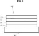
- FIG. 2 shows an inverted OLED 200.
- the device includes a substrate 210, a cathode 215, an emissive layer 220, a hole transport layer 225, and an anode 230.
- Device 200 may be fabricated by depositing the layers described, in order. Because the most common OLED configuration has a cathode disposed over the anode, and device 200 has cathode 215 disposed under anode 230, device 200 may be referred to as an "inverted" OLED. Materials similar to those described with respect to device 100 may be used in the corresponding layers of device 200.
- FIG. 2 provides one example of how some layers may be omitted from the structure of device 100.
- FIGS. 1 and 2 The simple layered structure illustrated in FIGS. 1 and 2 is provided by way of non-limiting example, and it is understood that embodiments of the invention may be used in connection with a wide variety of other structures.
- the specific materials and structures described are exemplary in nature, and other materials and structures may be used.
- Functional OLEDs may be achieved by combining the various layers described in different ways, or layers may be omitted entirely, based on design, performance, and cost factors. Other layers not specifically described may also be included. Materials other than those specifically described may be used. Although many of the examples provided herein describe various layers as comprising a single material, it is understood that combinations of materials, such as a mixture of host and dopant, or more generally a mixture, may be used. Also, the layers may have various sublayers.
- hole transport layer 225 transports holes and injects holes into emissive layer 220, and may be described as a hole transport layer or a hole injection layer.
- an OLED may be described as having an "organic layer" disposed between a cathode and an anode. This organic layer may comprise a single layer, or may further comprise multiple layers of different organic materials as described, for example, with respect to FIGS. 1 and 2 .
- OLEDs comprised of polymeric materials (PLEDs) such as disclosed in U.S. Pat. No. 5,247,190 to Friend et al. , which is incorporated by reference in its entirety.
- PLEDs polymeric materials
- OLEDs having a single organic layer may be used.
- OLEDs may be stacked, for example as described in U.S. Pat. No. 5,707,745 to Forrest et al , which is incorporated by reference in its entirety.
- the OLED structure may deviate from the simple layered structure illustrated in FIGS. 1 and 2 .
- the substrate may include an angled reflective surface to improve out-coupling, such as a mesa structure as described in U.S. Pat. No. 6,091,195 to Forrest et al. , and/or a pit structure as described in U.S. Pat. No. 5,834,893 to Bulovic et al. , which are incorporated by reference in their entireties.
- emissive layers or materials may include quantum dots.
- An "emissive layer” or “emissive material” as disclosed herein may include an organic emissive material and/or an emissive material that contains quantum dots or equivalent structures, unless indicated to the contrary explicitly or by context according to the understanding of one of skill in the art.
- Such an emissive layer may include only a quantum dot material which converts light emitted by a separate emissive material or other emitter, or it may also include the separate emissive material or other emitter, or it may emit light itself directly from the application of an electric current.
- a color altering layer, color filter, upconversion, or downconversion layer or structure may include a material containing quantum dots, though such layer may not be considered an "emissive layer" as disclosed herein.
- an "emissive layer” or material is one that emits an initial light, which may be altered by another layer such as a color filter or other color altering layer that does not itself emit an initial light within the device, but may re-emit altered light of a different spectra content based upon initial light emitted by the emissive layer.
- any of the layers of the various embodiments may be deposited by any suitable method.
- preferred methods include thermal evaporation, ink-jet, such as described in U.S. Pat. Nos. 6,013,982 and 6,087,196 , which are incorporated by reference in their entireties, organic vapor phase deposition (OVPD), such as described in U.S. Pat. No. 6,337,102 to Forrest et al. , which is incorporated by reference in its entirety, and deposition by organic vapor jet printing (OVJP), such as described in U.S. Pat. No. 7,431,968 , which is incorporated by reference in its entirety.
- OVPD organic vapor phase deposition
- OJP organic vapor jet printing
- Other suitable deposition methods include spin coating and other solution based processes.
- Solution based processes are preferably carried out in nitrogen or an inert atmosphere.
- preferred methods include thermal evaporation.
- Preferred patterning methods include deposition through a mask, cold welding such as described in U.S. Pat. Nos. 6,294,398 and 6,468,819 , which are incorporated by reference in their entireties, and patterning associated with some of the deposition methods such as ink-jet and OVJD. Other methods may also be used.
- the materials to be deposited may be modified to make them compatible with a particular deposition method. For example, substituents such as alkyl and aryl groups, branched or unbranched, and preferably containing at least 3 carbons, may be used in small molecules to enhance their ability to undergo solution processing.
- Such consumer products would include any kind of products that include one or more light source(s) and/or one or more of some type of visual displays.
- Some examples of such consumer products include flat panel displays, computer monitors, medical monitors, televisions, billboards, lights for interior or exterior illumination and/or signaling, heads-up displays, fully or partially transparent displays, flexible displays, laser printers, telephones, mobile phones, tablets, phablets, personal digital assistants (PDAs), wearable devices, laptop computers, digital cameras, camcorders, viewfinders, micro-displays (displays that are less than 2 inches diagonal), 3-D displays, virtual reality or augmented reality displays, vehicles, video walls comprising multiple displays tiled together, theater or stadium screen, and a sign.
- control mechanisms may be used to control devices fabricated in accordance with the present invention, including passive matrix and active matrix. Many of the devices are intended for use in a temperature range comfortable to humans, such as 18 C to 30 C, and more preferably at room temperature (20-25 C), but could be used outside this temperature range, for example, from -40 C to 80 C.
- the peak maximum wavelength of the phosphorescent dopant may be greater than or equal to 610 nm, greater than or equal to 620 nm, greater than or equal to 630 nm, greater than or equal to 650 nm, greater than or equal to 700 nm, greater than or equal to 750 nm, or greater than or equal to 800 nm.
- the hole blocking layer may include the compound of Formula I, which may be one or more of: and R 1 , R 2 and R 3 each may independently represent mono to the maximum allowable substitution, or no substitution.
- R 1 , R 2 and R 3 may be independently a hydrogen or deuterium, halogen, alkyl, cycloalkyl, heteroalkyl, heterocycloalkyl, arylalkyl, alkoxy, aryloxy, amino, silyl, alkenyl, cycloalkenyl, heteroalkenyl, alkynyl, aryl, heteroaryl, acyl, carboxylic acid, ether, ester, nitrile, isonitrile, sulfanyl, sulfinyl, sulfonyl, phosphino, and/or combinations thereof.
- Each X may be independently N, CH, or CR 3 .
- Y may be O, S, Se, NAr 4 , CAr 4 Ar 5 , SiAr 4 Ar 5 , Fluorene (C-Ar 1 Ar 2 ), and/or Silicon (Si-Ar 1 Ar 2 ), where Ar 1 and Ar 2 may be the same or different aryl groups.
- Each Ar 1 -Ar 5 may be independently selected from aryl, heteroaryl, and/or a combination thereof, and L may be a direct bond or a linker comprising at least one aromatic ring.
- Each R 1 , R 2 and R 3 may be independently a hydrogen or a substituent such as aryl, heteroaryl, and/or combinations thereof.
- Each X may be independently N, or CH.
- Y may be O, S, and/or NAr 4 .
- the compound of Formula I may be the only compound in the hole blocking layer.
- the compound of Formula I may be one or more of:
- the phosphorescent dopant may emit light from a triplet excited state to a ground singlet state in the device at room temperature.
- the phosphorescent dopant may be a metal coordination complex having a metal-carbon bond.
- the metal may be Ir, Os, Pt, Pd, Ag, Au, or Cu.
- the metal coordination complex may include a ligand having a chemical moiety of pyridazine, pyrimidine, pyrazine, and/or triazine.
- the metal coordination complex may have the formula of Ir(L A ) 3 , Ir(L A )(L B ) 2 , Ir(L A ) 2 (L B ), Ir(L A ) 2 (L C ), or Ir(L A )(L B )(L C ), where L A , L B , and L C are different from each other.
- the metal coordination complex may have a formula of Pt(L A )(L B ), where L A , and L B can be same or different, and where L A , and L B may be optionally connected to form a tetradentate ligand.
- the metal coordination complex may have a formula of Ir(L A ) 2 (L C ), where L A is selected from: where Lc is and where each R A , and R B may independently represent from mono substitution to the maximum possible number of substitution, or no substitution.
- Each R A , and R B may be independently selected from: hydrogen, deuterium, halogen, alkyl, cycloalkyl, heteroalkyl, heterocycloalkyl, arylalkyl, alkoxy, aryloxy, amino, silyl, alkenyl, cycloalkenyl, heteroalkenyl, alkynyl, aryl, heteroaryl, acyl, carboxylic acid, ether, ester, nitrile, isonitrile, sulfanyl, sulfinyl, sulfonyl, phosphino, and combinations thereof. Any two adjacent substituents of R A , and R B may be optionally fused or joined to form a ring or form
- the metal coordination complex may be selected from: and and
- the metal coordination complex may be a Pt complex having a tetradentate ligand.
- the tetradentate ligand may have four coordination atoms selected from: (two anionic C, two neutral N); (one anionic C, one carbene C, one neutral N, and one anionic N); (two anionic C, one carbene C, one neutral N); (one anionic C, one anionic N, two neutral N); (one anionic C, one anionic O, two neutral N); (two carbene C, two anionic N.
- the electron blocking layer may include the compound of Formula II: where R 3 , R 4 , and R 5 may each independently represent mono to the maximum allowable substitution, or no substitution, where each R 3 , R 4 , and R 5 may be independently a hydrogen or a substituent selected from deuterium, halogen, alkyl, cycloalkyl, heteroalkyl, heterocycloalkyl, arylalkyl, alkoxy, aryloxy, amino, silyl, alkenyl, cycloalkenyl, heteroalkenyl, alkynyl, aryl, heteroaryl, acyl, carboxylic acid, ether, ester, nitrile, isonitrile, sulfanyl, sulfinyl, sulfonyl, phosphino, and/or combinations thereof, and where each Ar 5 and Ar 6 may be independently selected from aryl, heteroaryl, and/or combination thereof.
- R 3 , R 4 , and R 5 may independently
- the electron blocking layer may include a compound selected from:
- the OLED has one or more characteristics selected from the group consisting of being flexible, being rollable, being foldable, being stretchable, and being curved. In some embodiments, the OLED is transparent or semi-transparent. In some embodiments, the OLED further comprises a layer comprising carbon nanotubes.
- the OLED further comprises a layer comprising a delayed fluorescent emitter.
- the OLED comprises a RGB pixel arrangement or white plus color filter pixel arrangement.
- the OLED is a mobile device, a hand held device, or a wearable device.
- the OLED is a display panel having less than 10 inch diagonal or 50 square inch area.
- the OLED is a display panel having at least 10 inch diagonal or 50 square inch area.
- the OLED is a lighting panel.
- the emissive region further comprises a host.
- the compound can be an emissive dopant.
- the compound can produce emissions via phosphorescence, fluorescence, thermally activated delayed fluorescence, i.e., TADF (also referred to as E-type delayed fluorescence), triplet-triplet annihilation, or combinations of these processes.
- TADF thermally activated delayed fluorescence
- the OLED disclosed herein can be incorporated into one or more of a consumer product, an electronic component module, and a lighting panel.
- the organic layer can be an emissive layer and the compound can be an emissive dopant in some embodiments, while the compound can be a non-emissive dopant in other embodiments.
- the organic layer can also include a host.
- a host In some embodiments, two or more hosts are preferred.
- the hosts used maybe a) bipolar, b) electron transporting, c) hole transporting or d) wide band gap materials that play little role in charge transport.
- the host can include a metal complex.
- the host can be an inorganic compound.
- a charge transport layer can be doped with conductivity dopants to substantially alter its density of charge carriers, which will in turn alter its conductivity.
- the conductivity is increased by generating charge carriers in the matrix material, and depending on the type of dopant, a change in the Fermi level of the semiconductor may also be achieved.
- Hole-transporting layer can be doped by p-type conductivity dopants and n-type conductivity dopants are used in the electron-transporting layer.
- a hole injecting/transporting material to be used in the present invention is not particularly limited, and any compound may be used as long as the compound is typically used as a hole injecting/transporting material.
- An electron blocking layer may be used to reduce the number of electrons and/or excitons that leave the emissive layer.
- the presence of such a blocking layer in a device may result in substantially higher efficiencies, and or longer lifetime, as compared to a similar device lacking a blocking layer.
- a blocking layer may be used to confine emission to a desired region of an OLED.
- the EBL material has a higher LUMO (closer to the vacuum level) and/or higher triplet energy than the emitter closest to the EBL interface.
- the EBL material has a higher LUMO (closer to the vacuum level) and or higher triplet energy than one or more of the hosts closest to the EBL interface.
- the compound used in EBL contains the same molecule or the same functional groups used as one of the hosts described below.
- the light emitting layer of the organic EL device of the present invention preferably contains at least a metal complex as light emitting material, and may contain a host material using the metal complex as a dopant material.
- the host material are not particularly limited, and any metal complexes or organic compounds may be used as long as the triplet energy of the host is larger than that of the dopant. Any host material may be used with any dopant so long as the triplet criteria is satisfied.
- a hole blocking layer may be used to reduce the number of holes and/or excitons that leave the emissive layer.
- the presence of such a blocking layer in a device may result in substantially higher efficiencies and/or longer lifetime as compared to a similar device lacking a blocking layer.
- a blocking layer may be used to confine emission to a desired region of an OLED.
- the HBL material has a lower HOMO (further from the vacuum level) and or higher triplet energy than the emitter closest to the HBL interface.
- the HBL material has a lower HOMO (further from the vacuum level) and or higher triplet energy than one or more of the hosts closest to the HBL interface.
- An electron transport layer may include a material capable of transporting electrons.
- the electron transport layer may be intrinsic (undoped), or doped. Doping may be used to enhance conductivity. Examples of the ETL material are not particularly limited, and any metal complexes or organic compounds may be used as long as they are typically used to transport electrons.
- the CGL plays an essential role in the performance, which is composed of an n-doped layer and a p-doped layer for injection of electrons and holes, respectively. Electrons and holes are supplied from the CGL and electrodes. The consumed electrons and holes in the CGL are refilled by the electrons and holes injected from the cathode and anode, respectively; then, the bipolar currents reach a steady state gradually.
- Typical CGL materials include n and p conductivity dopants used in the transport layers.
- Deep HOMO emitters may be PHOLED (phosphorescent organic light emitting diode) emitters with narrow spectrum, high LE / EQE (luminous efficacy/external quantum efficiency) ratio, long lifetime, and an EQE value above a predetermined amount.
- the narrow spectrum of the deep HOMO emitters may have full width at half maximum (FHWM) values of less than 50 nm, less than 45 nm, less than 40 nm, or the like. Due to narrow electroluminescent (EL) spectrum, the amount of photon emitting in invisible range over 670 nm may be minimized compared to conventional broad red emitters, and thus less photons losses may occur. Most of the emitted photons may be in the visible range, which may provide for higher luminance efficiency at the same EQE for the narrow EL emitters.
- FHWM full width at half maximum
- EL electroluminescent
- HOMO levels e.g., ⁇ -5.3 eV
- broad emitters e.g., ⁇ -5.1 eV
- Embodiments of the disclosed subject matter may provide a different approach for the efficient device structure architecture for deep HOMO emitters, such as for deep HOMO red emitters.
- narrow EL emitters may have deeper HOMO level (e.g., ⁇ 5.3 eV) when compared to the HOMO level for broad emitters (e.g., ⁇ 5.1 eV). This may cause different behavior of the emitter in the device, and different device structure architecture for deep HOMO emitters may be used.
- HOMO level e.g., ⁇ 5.3 eV
- broad emitters e.g., ⁇ 5.1 eV
- Embodiments of the disclosed subject matter provide designs for an efficient device structure for deep HOMO emitters.
- a hole blocking layer (HBL) may affect the efficiency of deep HOMO RD1 emitter device, whereas an electron blocking layer (EBL) may not affect efficiency (e.g., as shown in examples 1, 2, 3, 4 of Table 2).
- HBL hole blocking layer
- EBL electron blocking layer
- the RD1 device may have a recombination zone close to the HBL side of EML (emissive layer).
- the HBL may improve RD1 device efficiency by preventing exciton quenching and electron leakage to the ETL (electron transport layer).
- the RD2 device may have a recombination zone (RZ) close to the EBL, and the EBL may improve device efficiency by prevention of exciton quenching and hole leakage to the HTL (hole transport layer).
- Deep HOMO RD1 may provide improved hole transport to the HBL side of EML, as there may be less hole trapping.
- the reference shallow HOMO RD2 may not provide enough hole transport through the EML, as there may be more hole trapping.
- the RZ may be localized so as to be in the proximity of EBL.
- Embodiments of the disclosed subject matter may provide for the combination of the deep HOMO emitter and HBL to provide improved device efficiency.
- Efficiency roll off with luminance increase may be a problem for phosphorescent devices, and reduction of efficiency roll-off may be important in order to provide increased device efficiency at higher luminances.
- EQE roll off may be calculated as ratio of EQE at 10 mA/cm 2 to EQE of 1 ma/cm 2 for the same device (see, e.g., last column in Table 2).
- Data in Table 2 and FIG. 6 shows that HBL may provide efficiency roll-off reduction for the RD1 deep HOMO emitter (see, e.g., Example 1 vs. Example 2 and Example 3 vs. Example 4 in Table 2) and may have no or minimal roll off effect on a device with an RD2 emitter (see, e.g., Example 6 vs. Example 5 and Example 7 vs. Example 8 in Table 2).
- All example devices were fabricated by high vacuum ( ⁇ 10 -7 Torr) thermal evaporation.
- the anode electrode was 1,150 ⁇ of indium tin oxide (ITO).
- the cathode was comprised of 10 ⁇ of Liq (8-hydroxyquinoline lithium) followed by 1,000 ⁇ of Al. All devices were encapsulated with a glass lid sealed with an epoxy resin in a nitrogen glove box ( ⁇ 1 ppm of H 2 O and O 2 ) immediately after fabrication, and a moisture getter was incorporated inside the package.
- HIL hole injection layer
- HTL hole transporting layer
- EBM electron blocking material
- EBL electron blocking layer
- EML an emissive layer
Landscapes
- Physics & Mathematics (AREA)
- Chemical & Material Sciences (AREA)
- Engineering & Computer Science (AREA)
- Materials Engineering (AREA)
- Optics & Photonics (AREA)
- Spectroscopy & Molecular Physics (AREA)
- Organic Chemistry (AREA)
- Crystallography & Structural Chemistry (AREA)
- Inorganic Chemistry (AREA)
- Electroluminescent Light Sources (AREA)
- Nanotechnology (AREA)
Abstract
Description
- This application claims priority to
U.S. Patent Application Serial No. 62/749,290, filed October 23, 2018 - The present invention relates to compounds for use as emitters, and devices, such as organic light emitting diodes, including the same.
- Opto-electronic devices that make use of organic materials are becoming increasingly desirable for a number of reasons. Many of the materials used to make such devices are relatively inexpensive, so organic opto-electronic devices have the potential for cost advantages over inorganic devices. In addition, the inherent properties of organic materials, such as their flexibility, may make them well suited for particular applications such as fabrication on a flexible substrate. Examples of organic opto-electronic devices include organic light emitting diodes/devices (OLEDs), organic phototransistors, organic photovoltaic cells, and organic photodetectors. For OLEDs, the organic materials may have performance advantages over conventional materials. For example, the wavelength at which an organic emissive layer emits light may generally be readily tuned with appropriate dopants.
- OLEDs make use of thin organic films that emit light when voltage is applied across the device. OLEDs are becoming an increasingly interesting technology for use in applications such as flat panel displays, illumination, and backlighting. Several OLED materials and configurations are described in
U.S. Pat. Nos. 5,844,363 ,6,303,238 , and5,707,745 , which are incorporated herein by reference in their entirety. - One application for phosphorescent emissive molecules is a full color display. Industry standards for such a display call for pixels adapted to emit particular colors, referred to as "saturated" colors. In particular, these standards call for saturated red, green, and blue pixels. Alternatively the OLED can be designed to emit white light. In conventional liquid crystal displays emission from a white backlight is filtered using absorption filters to produce red, green and blue emission. The same technique can also be used with OLEDs. The white OLED can be either a single EML device or a stack structure. Color may be measured using CIE coordinates, which are well known to the art.
- As used herein, the term "organic" includes polymeric materials as well as small molecule organic materials that may be used to fabricate organic opto-electronic devices. "Small molecule" refers to any organic material that is not a polymer, and "small molecules" may actually be quite large. Small molecules may include repeat units in some circumstances. For example, using a long chain alkyl group as a substituent does not remove a molecule from the "small molecule" class. Small molecules may also be incorporated into polymers, for example as a pendent group on a polymer backbone or as a part of the backbone. Small molecules may also serve as the core moiety of a dendrimer, which consists of a series of chemical shells built on the core moiety. The core moiety of a dendrimer may be a fluorescent or phosphorescent small molecule emitter. A dendrimer may be a "small molecule," and it is believed that all dendrimers currently used in the field of OLEDs are small molecules.
- As used herein, "top" means furthest away from the substrate, while "bottom" means closest to the substrate. Where a first layer is described as "disposed over" a second layer, the first layer is disposed further away from substrate. There may be other layers between the first and second layer, unless it is specified that the first layer is "in contact with" the second layer. For example, a cathode may be described as "disposed over" an anode, even though there are various organic layers in between.
- As used herein, "solution processible" means capable of being dissolved, dispersed, or transported in and/or deposited from a liquid medium, either in solution or suspension form.
- A ligand may be referred to as "photoactive" when it is believed that the ligand directly contributes to the photoactive properties of an emissive material. A ligand may be referred to as "ancillary" when it is believed that the ligand does not contribute to the photoactive properties of an emissive material, although an ancillary ligand may alter the properties of a photoactive ligand.
- As used herein, and as would be generally understood by one skilled in the art, a first "Highest Occupied Molecular Orbital" (HOMO) or "Lowest Unoccupied Molecular Orbital" (LUMO) energy level is "greater than" or "higher than" a second HOMO or LUMO energy level if the first energy level is closer to the vacuum energy level. Since ionization potentials (IP) are measured as a negative energy relative to a vacuum level, a higher HOMO energy level corresponds to an IP having a smaller absolute value (an IP that is less negative). Similarly, a higher LUMO energy level corresponds to an electron affinity (EA) having a smaller absolute value (an EA that is less negative). On a conventional energy level diagram, with the vacuum level at the top, the LUMO energy level of a material is higher than the HOMO energy level of the same material. A "higher" HOMO or LUMO energy level appears closer to the top of such a diagram than a "lower" HOMO or LUMO energy level.
- As used herein, and as would be generally understood by one skilled in the art, a first work function is "greater than" or "higher than" a second work function if the first work function has a higher absolute value. Because work functions are generally measured as negative numbers relative to vacuum level, this means that a "higher" work function is more negative. On a conventional energy level diagram, with the vacuum level at the top, a "higher" work function is illustrated as further away from the vacuum level in the downward direction. Thus, the definitions of HOMO and LUMO energy levels follow a different convention than work functions.
- More details on OLEDs, and the definitions described above, can be found in
US Pat. No. 7,279,704 , which is incorporated herein by reference in its entirety. - According to an embodiment, an organic light emitting diode/device (OLED) is also provided. The OLED can include an anode, a cathode, and an organic layer, disposed between the anode and the cathode. According to an embodiment, the organic light emitting device is incorporated into one or more device selected from a consumer product, an electronic component module, and/or a lighting panel.
- An embodiment of the disclosed subject matter may provide an organic light emitting diode (OLED) having an anode, a cathode, an emissive layer disposed between the anode and the cathode, and a hole blocking layer disposed between the emissive and the cathode. The emissive layer may include a phosphorescent dopant. The phosphorescent dopant may have an emission in 0.5% doped PMMA (Poly(methyl methacrylate)) thin film with a peak maximum wavelength that is greater than or equal to 600 nm at room temperature. The energy of a highest occupied molecular orbital (HOMO) of the phosphorescent dopant may be lower than or equal to -5.1 eV, and the energy of the HOMO of the hole blocking layer may be at least 0.1 eV lower than the energy of the HOMO of the phosphorescent dopant.
- The peak maximum wavelength of the phosphorescent dopant may be greater than or equal to 610 nm, greater than or equal to 620 nm, greater than or equal to 630 nm, greater than or equal to 650 nm, greater than or equal to 700 nm, greater than or equal to 750 nm, or greater than or equal to 800 nm.
- The OLED may have the hole blocking layer disposed on the emissive layer.
- The energy of the HOMO of the phosphorescent dopant may be lower than or equal to -5.2 eV, lower than or equal to -5.3 eV, or lower than or equal to -5.4 eV. The energy of the HOMO of the hole blocking layer may be at least 0.2 eV lower than the energy of the HOMO of the phosphorescent dopant, at least 0.3 eV lower than the energy of the HOMO of the phosphorescent dopant, or at least 0.4 eV lower than the energy of the HOMO of the phosphorescent dopant.
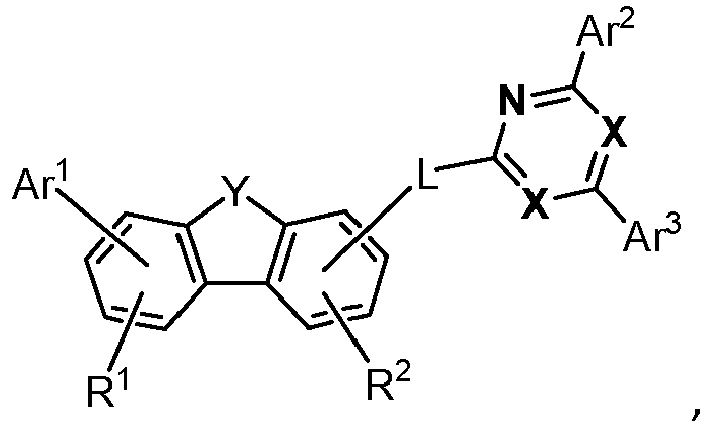
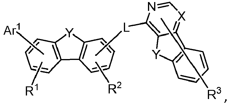
- The hole blocking layer may include the compound of Formula I, which may be one or more of:


- The compound of Formula I may be one or more of:

- The phosphorescent dopant may emit light from a triplet excited state to a ground singlet state in the device at room temperature. The phosphorescent dopant may be a metal coordination complex having a metal-carbon bond. The metal may be Ir, Os, Pt, Pd, Ag, Au, or Cu. The metal coordination complex may include a ligand having a chemical moiety of pyridazine, pyrimidine, pyrazine, and/or triazine. The metal coordination complex may have the formula of M(L1)x(Lz)y(L3)z, where L1, L2 and L3 may be the same or different, where x is 1, 2, or 3, where y is 0, 1, or 2, where z is 0, 1, or 2, where x+y+z is the oxidation state of the metal M, where L1, L2 and L3 may each independently selected from:


- The metal coordination complex may have the formula of Ir(LA)3, Ir(LA)(LB)2, Ir(LA)2(LB), Ir(LA)2(LC), or Ir(LA)(LB)(LC), where LA, LB, and LC are different from each other. The metal coordination complex may have a formula of Pt(LA)(LB), where LA, and LB can be same or different, and where LA, and LB may be optionally connected to form a tetradentate ligand.
- The metal coordination complex may have a formula of Ir(LA)2(LC), where LA is selected from:


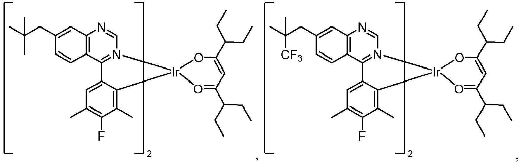
- The metal coordination complex may be selected from:




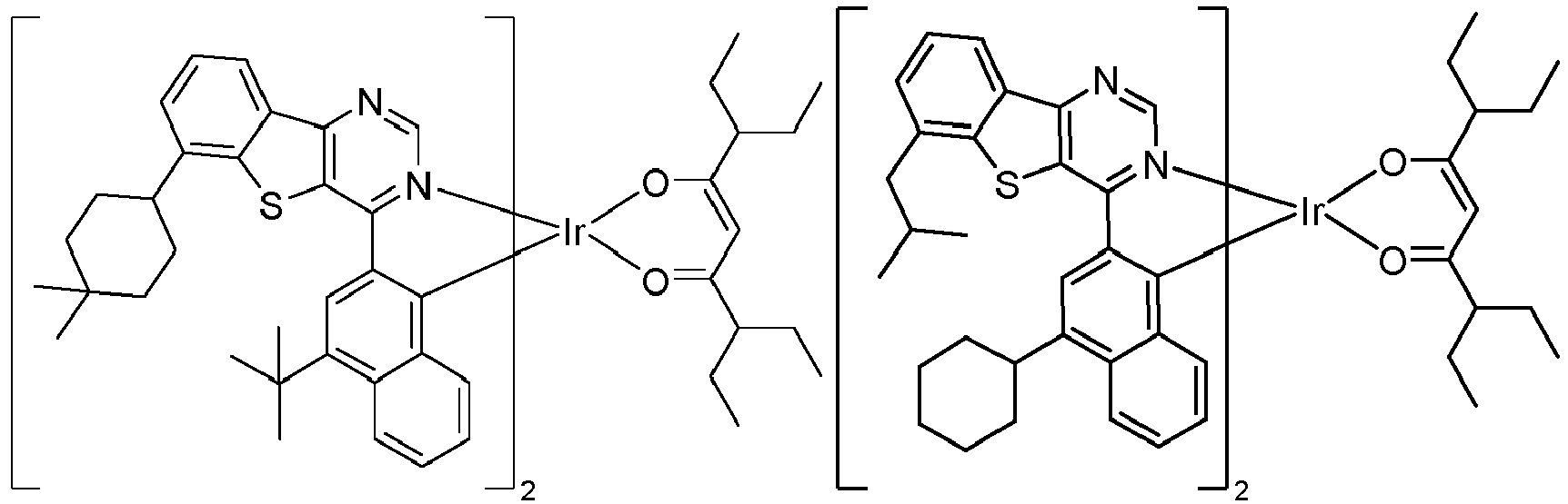


- The metal coordination complex may be a Pt complex having a tetradentate ligand. The tetradentate ligand may have four coordination atoms selected from: (two anionic C, two neutral N); (one anionic C, one carbene C, one neutral N, and one anionic N); (two anionic C, one carbene C, one neutral N); (one anionic C, one anionic N, two neutral N); (one anionic C, one anionic O, two neutral N); (two carbene C, two anionic N).
- The electron blocking layer may include the compound of Formula II:
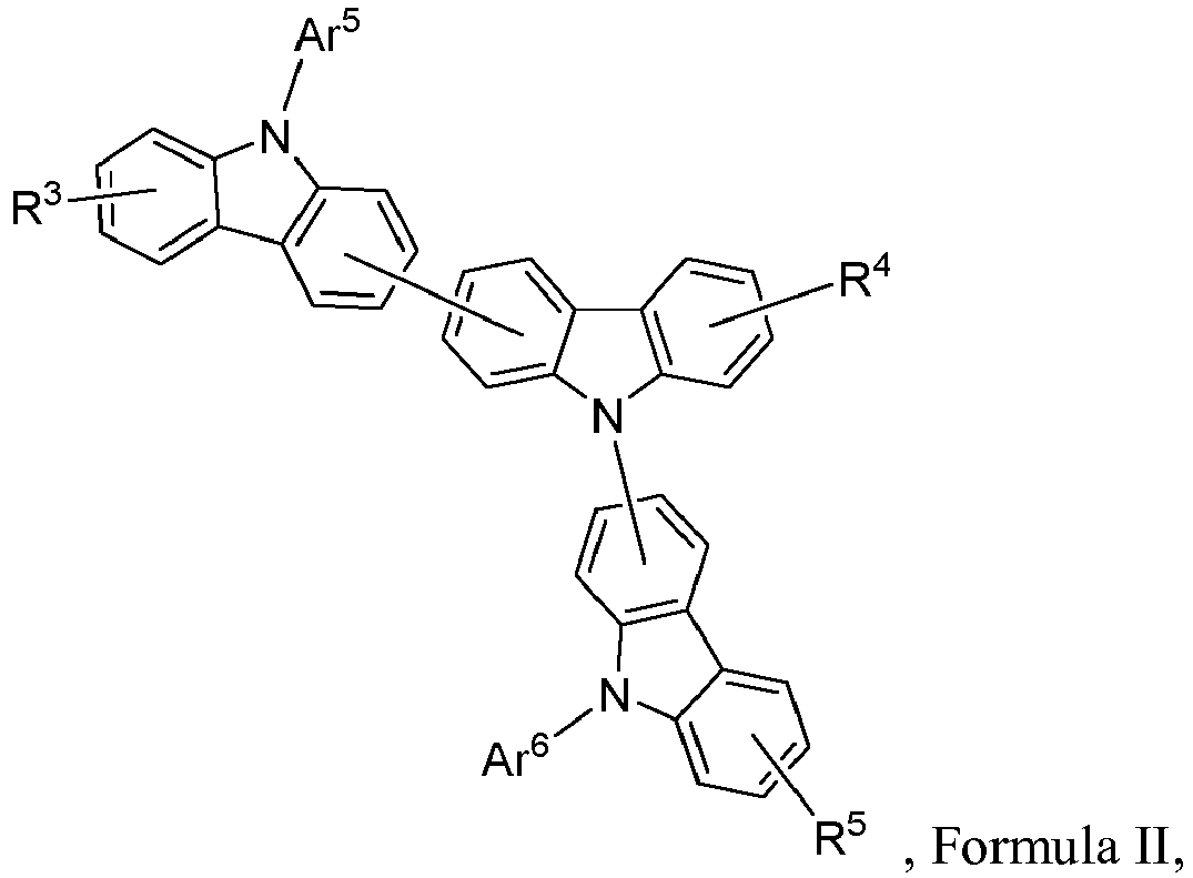
- In embodiments of the disclosed subject matter, the device may be at least one type selected from: a flat panel display, a computer monitor, a medical monitor, a television, a billboard, a light for interior or exterior illumination and/or signaling, a heads-up display, a fully or partially transparent display, a flexible display, a laser printer, a telephone, a mobile phone, a tablet, a phablet, a personal digital assistant (PDA), a wearable device, a laptop computer, a digital camera, a camcorder, a viewfinder, a micro-display having an active area with a primary diagonal of 2 inches or less, a 3-D display, a virtual reality or augmented reality display, a vehicle, a video wall comprising multiple displays tiled together, a theater or stadium screen, and a sign.
-
-
FIG. 1 shows an organic light emitting device. -
FIG. 2 shows an inverted organic light emitting device that does not have a separate electron transport layer. -
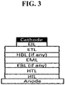
FIG. 3 shows an example device structure according to an embodiment of the disclosed subject matter. -
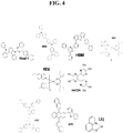
FIG. 4 shows example materials used in OLED (organic light emitting diode) devices according to embodiments of the disclosed subject matter. -
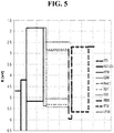
FIG. 5 shows an example PHOLED (phosphorescent organic light emitting diode) structure energy levels according to an embodiment of the disclosed subject matter. -
FIG. 6 shows a graph of external quantum efficiency (EQE) vs. current density for devices with RD1 and RD2 emitters according to embodiments of the disclosed subject matter. -
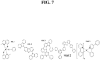
FIG. 7 shows device materials according to embodiments of the disclosed subject matter. - Generally, an OLED comprises at least one organic layer disposed between and electrically connected to an anode and a cathode. When a current is applied, the anode injects holes and the cathode injects electrons into the organic layer(s). The injected holes and electrons each migrate toward the oppositely charged electrode. When an electron and hole localize on the same molecule, an "exciton," which is a localized electron-hole pair having an excited energy state, is formed. Light is emitted when the exciton relaxes via a photoemissive mechanism. In some cases, the exciton may be localized on an excimer or an exciplex. Non-radiative mechanisms, such as thermal relaxation, may also occur, but are generally considered undesirable.
- The initial OLEDs used emissive molecules that emitted light from their singlet states ("fluorescence") as disclosed, for example, in
U.S. Pat. No. 4,769,292 , which is incorporated by reference in its entirety. Fluorescent emission generally occurs in a time frame of less than 10 nanoseconds. - More recently, OLEDs having emissive materials that emit light from triplet states ("phosphorescence") have been demonstrated. Baldo et al., "Highly Efficient Phosphorescent Emission from Organic Electroluminescent Devices," Nature, vol. 395, 151-154, 1998; ("Baldo-I") and Baldo et al., "Very high-efficiency green organic light-emitting devices based on electrophosphorescence," Appl. Phys. Lett., vol. 75, No. 3, 4-6 (1999) ("Baldo-II"), are incorporated by reference in their entireties. Phosphorescence is described in more detail in
US Pat. No. 7,279,704 at cols. 5-6, which are incorporated by reference. -
FIG. 1 shows an organiclight emitting device 100. The figures are not necessarily drawn to scale.Device 100 may include asubstrate 110, ananode 115, ahole injection layer 120, ahole transport layer 125, anelectron blocking layer 130, anemissive layer 135, ahole blocking layer 140, anelectron transport layer 145, anelectron injection layer 150, aprotective layer 155, acathode 160, and abarrier layer 170.Cathode 160 is a compound cathode having a firstconductive layer 162 and a secondconductive layer 164.Device 100 may be fabricated by depositing the layers described, in order. The properties and functions of these various layers, as well as example materials, are described in more detail inUS 7,279,704 at cols. 6-10, which are incorporated by reference. - More examples for each of these layers are available. For example, a flexible and transparent substrate-anode combination is disclosed in
U.S. Pat. No. 5,844,363 , which is incorporated by reference in its entirety. An example of a p-doped hole transport layer is m-MTDATA doped with F4-TCNQ at a molar ratio of 50:1, as disclosed inU.S. Patent Application Publication No. 2003/0230980 , which is incorporated by reference in its entirety. Examples of emissive and host materials are disclosed inU.S. Pat. No. 6,303,238 to Thompson et al ., which is incorporated by reference in its entirety. An example of an n-doped electron transport layer is BPhen doped with Li at a molar ratio of 1:1, as disclosed inU.S. Patent Application Publication No. 2003/0230980 , which is incorporated by reference in its entirety.U.S. Pat. Nos. 5,703,436 and5,707,745 , which are incorporated by reference in their entireties, disclose examples of cathodes including compound cathodes having a thin layer of metal such as Mg:Ag with an overlying transparent, electrically-conductive, sputter-deposited ITO layer. The theory and use of blocking layers is described in more detail inU.S. Pat. No. 6,097,147 andU.S. Patent Application Publication No. 2003/0230980 , which are incorporated by reference in their entireties. Examples of injection layers are provided inU.S. Patent Application Publication No. 2004/0174116 , which is incorporated by reference in its entirety. A description of protective layers may be found inU.S. Patent Application Publication No. 2004/0174116 , which is incorporated by reference in its entirety. -
FIG. 2 shows aninverted OLED 200. The device includes asubstrate 210, acathode 215, anemissive layer 220, ahole transport layer 225, and ananode 230.Device 200 may be fabricated by depositing the layers described, in order. Because the most common OLED configuration has a cathode disposed over the anode, anddevice 200 hascathode 215 disposed underanode 230,device 200 may be referred to as an "inverted" OLED. Materials similar to those described with respect todevice 100 may be used in the corresponding layers ofdevice 200.FIG. 2 provides one example of how some layers may be omitted from the structure ofdevice 100. - The simple layered structure illustrated in
FIGS. 1 and2 is provided by way of non-limiting example, and it is understood that embodiments of the invention may be used in connection with a wide variety of other structures. The specific materials and structures described are exemplary in nature, and other materials and structures may be used. Functional OLEDs may be achieved by combining the various layers described in different ways, or layers may be omitted entirely, based on design, performance, and cost factors. Other layers not specifically described may also be included. Materials other than those specifically described may be used. Although many of the examples provided herein describe various layers as comprising a single material, it is understood that combinations of materials, such as a mixture of host and dopant, or more generally a mixture, may be used. Also, the layers may have various sublayers. The names given to the various layers herein are not intended to be strictly limiting. For example, indevice 200,hole transport layer 225 transports holes and injects holes intoemissive layer 220, and may be described as a hole transport layer or a hole injection layer. In one embodiment, an OLED may be described as having an "organic layer" disposed between a cathode and an anode. This organic layer may comprise a single layer, or may further comprise multiple layers of different organic materials as described, for example, with respect toFIGS. 1 and2 . - Structures and materials not specifically described may also be used, such as OLEDs comprised of polymeric materials (PLEDs) such as disclosed in
U.S. Pat. No. 5,247,190 to Friend et al. , which is incorporated by reference in its entirety. By way of further example, OLEDs having a single organic layer may be used. OLEDs may be stacked, for example as described inU.S. Pat. No. 5,707,745 to Forrest et al , which is incorporated by reference in its entirety. The OLED structure may deviate from the simple layered structure illustrated inFIGS. 1 and2 . For example, the substrate may include an angled reflective surface to improve out-coupling, such as a mesa structure as described inU.S. Pat. No. 6,091,195 to Forrest et al. , and/or a pit structure as described inU.S. Pat. No. 5,834,893 to Bulovic et al. , which are incorporated by reference in their entireties. - In some embodiments disclosed herein, emissive layers or materials, such as
emissive layer 135 andemissive layer 220 shown inFIGS. 1-2 , respectively, may include quantum dots. An "emissive layer" or "emissive material" as disclosed herein may include an organic emissive material and/or an emissive material that contains quantum dots or equivalent structures, unless indicated to the contrary explicitly or by context according to the understanding of one of skill in the art. Such an emissive layer may include only a quantum dot material which converts light emitted by a separate emissive material or other emitter, or it may also include the separate emissive material or other emitter, or it may emit light itself directly from the application of an electric current. Similarly, a color altering layer, color filter, upconversion, or downconversion layer or structure may include a material containing quantum dots, though such layer may not be considered an "emissive layer" as disclosed herein. In general, an "emissive layer" or material is one that emits an initial light, which may be altered by another layer such as a color filter or other color altering layer that does not itself emit an initial light within the device, but may re-emit altered light of a different spectra content based upon initial light emitted by the emissive layer. - Unless otherwise specified, any of the layers of the various embodiments may be deposited by any suitable method. For the organic layers, preferred methods include thermal evaporation, ink-jet, such as described in
U.S. Pat. Nos. 6,013,982 and6,087,196 , which are incorporated by reference in their entireties, organic vapor phase deposition (OVPD), such as described inU.S. Pat. No. 6,337,102 to Forrest et al. , which is incorporated by reference in its entirety, and deposition by organic vapor jet printing (OVJP), such as described inU.S. Pat. No. 7,431,968 , which is incorporated by reference in its entirety. Other suitable deposition methods include spin coating and other solution based processes. Solution based processes are preferably carried out in nitrogen or an inert atmosphere. For the other layers, preferred methods include thermal evaporation. Preferred patterning methods include deposition through a mask, cold welding such as described inU.S. Pat. Nos. 6,294,398 and6,468,819 , which are incorporated by reference in their entireties, and patterning associated with some of the deposition methods such as ink-jet and OVJD. Other methods may also be used. The materials to be deposited may be modified to make them compatible with a particular deposition method. For example, substituents such as alkyl and aryl groups, branched or unbranched, and preferably containing at least 3 carbons, may be used in small molecules to enhance their ability to undergo solution processing. Substituents having 20 carbons or more may be used, and 3-20 carbons is a preferred range. Materials with asymmetric structures may have better solution processibility than those having symmetric structures, because asymmetric materials may have a lower tendency to recrystallize. Dendrimer substituents may be used to enhance the ability of small molecules to undergo solution processing. - Devices fabricated in accordance with embodiments of the present invention may further optionally comprise a barrier layer. One purpose of the barrier layer is to protect the electrodes and organic layers from damaging exposure to harmful species in the environment including moisture, vapor and/or gases, etc. The barrier layer may be deposited over, under or next to a substrate, an electrode, or over any other parts of a device including an edge. The barrier layer may comprise a single layer, or multiple layers. The barrier layer may be formed by various known chemical vapor deposition techniques and may include compositions having a single phase as well as compositions having multiple phases. Any suitable material or combination of materials may be used for the barrier layer. The barrier layer may incorporate an inorganic or an organic compound or both. The preferred barrier layer comprises a mixture of a polymeric material and a non-polymeric material as described in
U.S. Pat. No. 7,968,146 , PCT Pat. Application Nos.PCT/US2007/023098 andPCT/US2009/042829 , which are herein incorporated by reference in their entireties. To be considered a "mixture", the aforesaid polymeric and non-polymeric materials comprising the barrier layer should be deposited under the same reaction conditions and/or at the same time. The weight ratio of polymeric to non-polymeric material may be in the range of 95:5 to 5:95. The polymeric material and the non-polymeric material may be created from the same precursor material. In one example, the mixture of a polymeric material and a non-polymeric material consists essentially of polymeric silicon and inorganic silicon. - Devices fabricated in accordance with embodiments of the invention can be incorporated into a wide variety of electronic component modules (or units) that can be incorporated into a variety of electronic products or intermediate components. Examples of such electronic products or intermediate components include display screens, lighting devices such as discrete light source devices or lighting panels, etc. that can be utilized by the end-user product manufacturers. Such electronic component modules can optionally include the driving electronics and/or power source(s). Devices fabricated in accordance with embodiments of the invention can be incorporated into a wide variety of consumer products that have one or more of the electronic component modules (or units) incorporated therein. A consumer product comprising an OLED that includes the compound of the present disclosure in the organic layer in the OLED is disclosed. Such consumer products would include any kind of products that include one or more light source(s) and/or one or more of some type of visual displays. Some examples of such consumer products include flat panel displays, computer monitors, medical monitors, televisions, billboards, lights for interior or exterior illumination and/or signaling, heads-up displays, fully or partially transparent displays, flexible displays, laser printers, telephones, mobile phones, tablets, phablets, personal digital assistants (PDAs), wearable devices, laptop computers, digital cameras, camcorders, viewfinders, micro-displays (displays that are less than 2 inches diagonal), 3-D displays, virtual reality or augmented reality displays, vehicles, video walls comprising multiple displays tiled together, theater or stadium screen, and a sign. Various control mechanisms may be used to control devices fabricated in accordance with the present invention, including passive matrix and active matrix. Many of the devices are intended for use in a temperature range comfortable to humans, such as 18 C to 30 C, and more preferably at room temperature (20-25 C), but could be used outside this temperature range, for example, from -40 C to 80 C.
- The materials and structures described herein may have applications in devices other than OLEDs. For example, other optoelectronic devices such as organic solar cells and organic photodetectors may employ the materials and structures. More generally, organic devices, such as organic transistors, may employ the materials and structures.
- Embodiments of the disclosed subject matter may provide an organic light emitting diode (OLED) having an anode, a cathode, an emissive layer disposed between the anode and the cathode, and a hole blocking layer disposed between the emissive and the cathode. The emissive layer may include a phosphorescent dopant. The phosphorescent dopant may have an emission in 0.5% doped PMMA (Poly(methyl methacrylate)) thin film with a peak maximum wavelength that is greater than or equal to 600 nm at room temperature. The energy of a highest occupied molecular orbital (HOMO) of the phosphorescent dopant may be lower than or equal to -5.1 eV, and the energy of the HOMO of the hole blocking layer may be at least 0.1 eV lower than the energy of the HOMO of the phosphorescent dopant. In some embodiments, the OLED may have the hole blocking layer disposed on the emissive layer.
- The peak maximum wavelength of the phosphorescent dopant may be greater than or equal to 610 nm, greater than or equal to 620 nm, greater than or equal to 630 nm, greater than or equal to 650 nm, greater than or equal to 700 nm, greater than or equal to 750 nm, or greater than or equal to 800 nm.
- The energy of the HOMO of the phosphorescent dopant may be lower than or equal to -5.2 eV, lower than or equal to -5.3 eV, or lower than or equal to -5.4 eV. The energy of the HOMO of the hole blocking layer may be at least 0.2 eV lower than the energy of the HOMO of the phosphorescent dopant, at least 0.3 eV lower than the energy of the HOMO of the phosphorescent dopant, or at least 0.4 eV lower than the energy of the HOMO of the phosphorescent dopant.
- The hole blocking layer may include the compound of Formula I, which may be one or more of:


- The compound of Formula I may be one or more of:

- In some embodiments, the compound of Formula I may be one or more of:
Compound A1 through A3, each represented by the formula Compound A4 through A6, each represented by the formula Compound A7 through A9, each represented by the formula 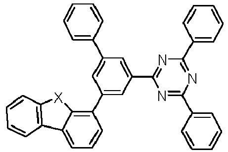


wherein in Compound A1: X=O, in Compound A2: X=S, in Compound A3: X=Se, wherein in Compound A4: X=O, in Compound A5: X=S, in Compound A6: X=Se, wherein in Compound A7: X=O, in Compound A8: X=S, in Compound A9: X=Se, Compound A10 through A12, each represented by the formula Compound A13 through A15, each represented by the formula Compound A16 through A18, each represented by the formula 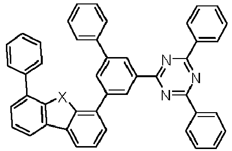


wherein in Compound A10: X=O, in Compound A11: X=S, in Compound A12: X=Se, wherein in Compound A13: X=O, in Compound A14: X=S, in Compound A15: X=Se, wherein in Compound A16: X=O, in Compound A17: X=S, in Compound A18: X=Se, Compound A19 through A21, each represented by the formula Compound A22 through A24, each represented by the formula Compound A25 through A27, each represented by the formula 


wherein in Compound A19: X=O, in Compound A20: X=S, in Compound A21: X=Se, wherein in Compound A22: X=O, in Compound A23: X=S, in Compound A24: X=Se, wherein in Compound A25: X=O, in Compound A26: X=S, in Compound A27: X=Se, Compound A28 through A30, each represented by the formula Compound A31 through A33, each represented by the formula Compound A34 through A36, each represented by the formula 


wherein in Compound A28: X=O, in Compound A29: X=S, in Compound A30: X=Se, wherein in Compound A31: X=O, in Compound A32: X=S, in Compound A33: X=Se, in compound A36: X=Se, Compound A37 through A39, each represented by the formula Compound A40 through A42, each represented by the formula Compound A43 through A45, each represented by the formula 

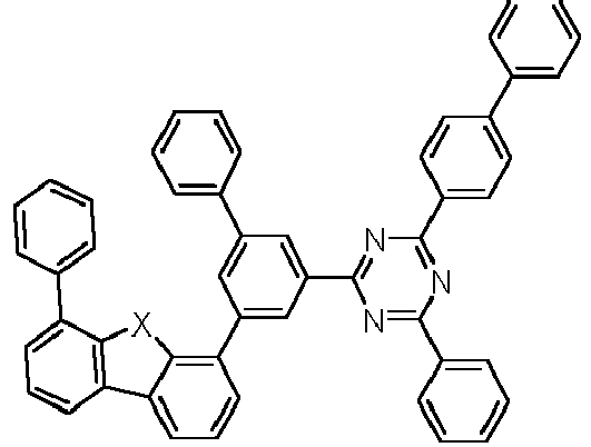
wherein in Compound A37: X=O, in Compound A38: X=S, in Compound A39: X=Se, wherein in Compound A40: X=O, in Compound A41: X=S, in Compound A42: X=Se, wherein in Compound A43: X=O, in Compound A44: X=S, in Compound A45: X=Se, Compound A46 through A48, each represented by the formula Compound A49 through A51, each represented by the formula Compound A52 through A54, each represented by the formula 


wherein in Compound A46: X=O, in Compound A47: X=S, in Compound A48: X=Se, wherein in Compound A49: X=O, in Compound A50: X=S, in Compound A51: X=Se, wherein in Compound A52: X=O, in Compound A53: X=S, in Compound A54: X=Se, Compound A55 through A57, each represented by the formula Compound A58 through A60, each represented by the formula Compound A61 through A63, each represented by the formula 
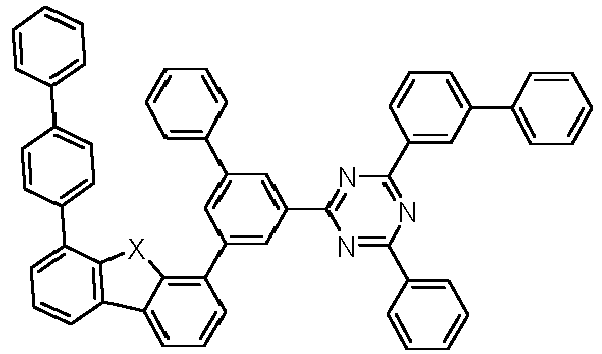

wherein in Compound A55: X=O, in Compound A56: X=S, in Compound A57: X=Se, wherein in Compound A58: X=O, in Compound A59: X=S, in Compound A60: X=Se, wherein in Compound A61: X=O, in Compound A62: X=S, in Compound A63: X=Se, Compound A64 through A66, each represented by the formula Compound A67 through A69, each represented by the formula Compound A70 through A72, each represented by the formula 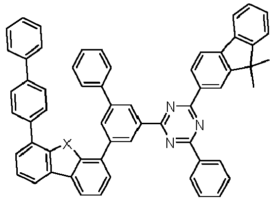


wherein in Compound A64: X=O, in Compound A65: X=S, in Compound A66: X=Se, wherein in Compound A67: X=O, in Compound A68: X=S, in Compound A69: X=Se, wherein in Compound A70: X=O, in Compound A71: X=S, in Compound A72: X=Se, Compound A73 through A75, each represented by the formula Compound A76 through A78, each represented by the formula Compound A79 through A81, each represented by the formula 


wherein in Compound A73: X=O, in Compound A74: X=S, in Compound A75: X=Se, wherein in Compound A76: X=O, in Compound A77: X=S, in Compound A78: X=Se, wherein in Compound A79: X=O, in Compound A80: X=S, in Compound A81: X=Se, Compound A82 through A84, each represented by the formula Compound A85 through A87, each represented by the formula Compound A88 through A90, each represented by the formula the formula 
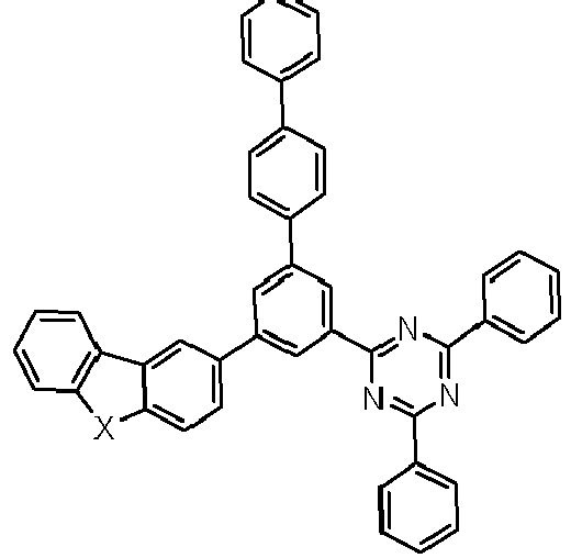
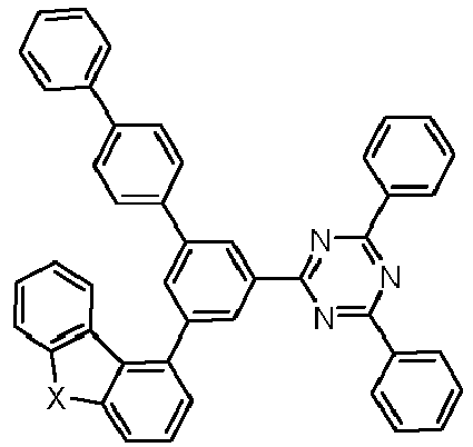
wherein in Compound A82: X=O, in Compound A83: X=S, in Compound A84: X=Se, wherein in Compound A85: X=O, in Compound A86: X=S, in Compound A87: X=Se, wherein in Compound A88: X=O, in Compound A89: X=S, in Compound A90: X=Se, Compound A91 through A93, each represented by the formula Compound A94 through A96, each represented by the formula Compound A97 through A99, each represented by the formula 


wherein in Compound A91: X=O, in Compound A92: X=S, in Compound A93: X=Se, wherein in Compound A94: X=O, in Compound A95: X=S, in Compound A96: X=Se, wherein in Compound A97: X=O, in Compound A98: X=S, in Compound A99: X=Se, Compound A100 through A102, each represented by the formula Compound A103 through A105, each represented by the formula 

wherein in Compound A100: X=O, in Compound A101: X=S, in Compound A102: X=Se, wherein in Compound A103: X=O, in Compound A104: X=S, in Compound A105: X=Se, Compound A106 through A108, each represented by the formula Compound A109 through A111, each represented by the formula 

wherein in Compound A106: X=O, in Compound A107: X=S, in Compound A108: X=Se, wherein in compound A109: X=O, in Compound A110: X=S, in Compound A111: X=Se, Compound A112 through A114, each represented by the formula Compound A115 through A117, each represented by the formula 


wherein in Compound A112: X=O, in Compound A113: X=S, in Compound A114: X=Se, wherein in Compound A115: X=O, in Compound A116: X=S, in Compound A117: X=Se, 


Compound C1 through C3, each represented by the formula Compound C4 through C6, each represented by the formula 
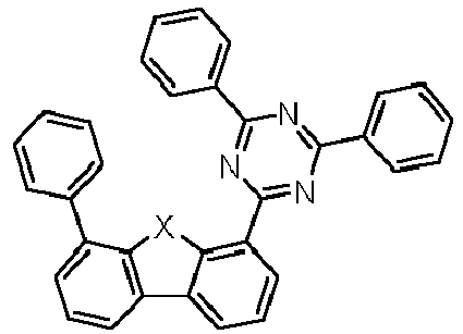

wherein in Compound C1: X=O, in Compound C2: X=S, in Compound C3: X=Se, wherein in Compound C4: X=O, in Compound C5: X=S, in Compound C6: X=Se, Compound C7 through C9, each represented by the formula Compound C10 through C12, each represented by the formula Compound C13 through C15, each represented by the formula 


wherein in Compound C7: X=O, in Compound C8: X=S, in Compound C9: X=Se, wherein in Compound C10: X=O, in Compound C11: X=S, in Compound C12: X=Se, wherein in Compound C13: X=O, in Compound C14: X=S, in Compound C15: X=Se, Compound C16 through C18, each represented by the formula Compound C19 through C21, each by the formula represented Compound C22 through C24, each represented by the formula 


wherein in Compound C16: X=O, in Compound C17: X=S, in Compound C18: X=Se, wherein in Compound C19: X=O, in Compound C20: X=S, in Compound C21: X=Se, wherein in Compound C22: X=O, in Compound C23: X=S, in Compound C24: X=Se, Compound C25 through C27, each represented by the formula Compound C28 through C30, each represented by the formula Compound C31 through C33, each represented by the formula 


wherein in Compound C25: X=O, in Compound C26: X=S, in Compound C27: X=Se, wherein in Compound C28: X=O, in Compound C29: X=S, in Compound C30: X=Se, wherein in Compound C31: X=O, in Compound C32: X=S, in Compound C33: X=Se, Compound C34 through C36, each represented by the formula Compound C37 through C39, each represented by the formula Compound C40 through C42, each represented by the formula 
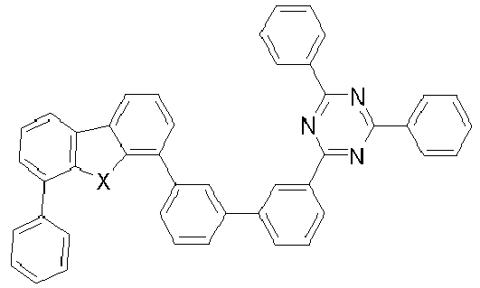

wherein in Compound C34: X=O, in Compound C35: X=S, in Compound C36: X=Se, wherein in Compound C37: X=O, in Compound C38: X=S,in Compound C39: X=Se, wherein in Compound C40: X=O, in Compound C41: X=S, in Compound C42: X=Se, Compound C43 through C45, each represented by the formula by Compound C46 through C48, each represented by the formula Compound C49 through C51, each represented by the formula 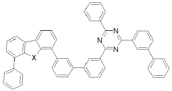


wherein in Compound C43: X=O, in Compound C44: X=S, in Compound C45: X=Se, wherein in Compound C46: X=O, in Compound C47: X=S, in Compound C48: X=Se, wherein in Compound C49: X=O, in Compound C50: X=S, in Compound C51: X=Se, Compound C52 through C54, each represented by the formula Compound C55 through C57, each represented by the formula Compound C58 through C60, each represented by the formula 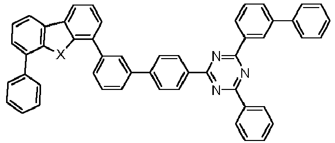


wherein in Compound C52: X=O, in Compound C53: X=S, in Compound C54: X=Se, wherein in Compound C55: X=O, in Compound C56: X=S, in Compound C57: X=Se, wherein in Compound C58: X=O, in Compound C59: X=S, in Compound C60: X=Se, Compound C61 through C63, each represented by the formula Compound C64 through C66, each represented by the formula Compound C67 through C69, each represented by the formula 


wherein in Compound C61: X=O, in Compound C62: X=S, in Compound C63: X=Se, wherein in Compound C64: X=O, in Compound C65: X=S, in Compound C66: X=Se, wherein in Compound C67: X=O, in Compound C68: X=S, in Compound C69: X=Se, Compound C70 through C72, each represented by the formula Compound C73 through C75, each represented by the formula Compound C76 through C78, each represented by the formula 


wherein in Compound C70: X=O, in Compound C71: X=S, in Compound C72: X=Se, wherein in Compound C73: X=O, in Compound C74: X=S, in Compound C75: X=Se, wherein in Compound C76: X=O, in Compound C77: X=S, in Compound C78: X=Se, Compound C79 through C81, each represented by the formula Compound C82 through C84, each represented by the formula Compound C85 through C87, each represented by the formula 


wherein in Compound C79: X=O, in Compound C80: X=S, in Compound C81: X=Se, wherein in Compound C82: X=O, in Compound C83: X=S, in Compound C84: X=Se, wherein in Compound C85: X=O, in Compound C86: X=S, in Compound C87: X=Se, Compound C88 through C90, each represented bv the formula Compound C91 through C93, each represented by the formula Compound C94 through C96, each represented by the formula 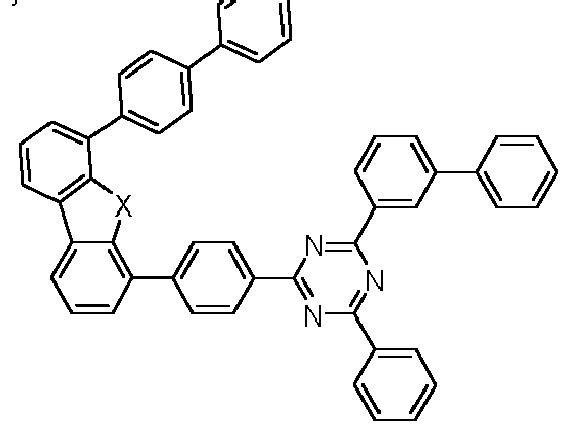
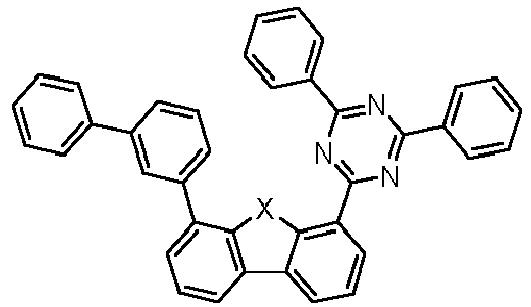

wherein in Compound C88: X=O, in Compound C89: X=S, in Compound C90: X=Se, wherein in Compound C91: X=O, in Compound C92: X=S, in Compound C93: X=Se, wherein in Compound C94: X=O, in Compound C95: X=S, in Compound C96: X=Se, Compound C97 through C99, each represented by the formula Compound C100 through C102, each represented by the formula Compound C103 through C105, each represented by the formula 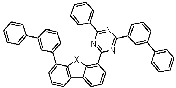


wherein in Compound C97: X=O, in Compound C98: X=S, in Compound C99: X=Se, wherein in Compound C100: X=O, in Compound C101: X=S, in Compound C102: X=Se, wherein in Compound C103: X=O, in Compound C104: X=S, in Compound C105: X=Se, Compound C106 through C108, each represented by the formula Compound C109 through C111, each represented by the formula 

wherein in Compound C106: X=O, in Compound C107: X=S, in Compound C108: X=Se, wherein in Compound C109: X=O, in Compound C110: X=S, in Compound C111: X=Se, Compound C112 through C114, each represented by the formula Compound C115 through C117, each represented by the formula 

wherein in Compound C112: X=O, in Compound C113: X=S, in Compound C114: X=Se, wherein in Compound C115: X=O, in Compound C116: X=S, in Compound C117: X=Se, Compound C118 through C120, each represented by the formula Compound C121 through C123, each represented by the formula 
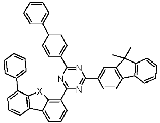
wherein in Compound C118: X=O, in Compound C119: X=S, in Compound C120: X=Se, wherein in Compound C121: X=O, in Compound C122: X=S, in Compound C123: X=Se, Compound C124 through C126, each represented by the formula Compound C127 through C129, each represented by the formula 

wherein in Compound C124: X=O, in Compound C125: X=S, in Compound C126: X=Se, wherein in Compound C127: X=O, in Compound C128: X=S, in Compound C129: X=Se, Compound C130 through C132, each represented by the formula Compound C133 through C135, each represented by the formula 

wherein in Compound C130: X=O, in Compound C131: X=S, in Compound C132: X=Se, wherein in Compound C133: X=O, in Compound C134: X=S, in Compound C135: X=Se, Compound C136 through C138, each represented by the formula Compound C139 through C141, each represented by the formula Compound C142 through C144, each represented by the formula 


wherein in Compound C136: X=O, in Compound C137: X=S, in Compound C138: X=Se, wherein in Compound C139: X=O, in Compound C140: X=S, in Compound C141: X=Se, wherein in Compound C142: X=O, in Compound C143: X=S, in Compound C144: X=Se, Compound C145 through C147, each represented by the formula Compound C148 through C150, each represented by the formula 

wherein in Compound C145: X=O, in Compound C146: X=S, in Compound C147: X=Se, wherein in Compound C148: X=O, in Compound C149: X=S, in Compound C150: X=Se, Compound C151 through C153, each represented by the formula Compound C154 through C156, each represented by the formula 

wherein in Compound C151: X=O, in Compound C152: X=S, in Compound C152: X=Se, wherein in Compound C154: X=O, in Compound C155: X=S, in Compound C156: X=Se, Compound C157 through C159, each represented by the formula Compound C160 through C162, each represented by the formula 

wherein in Compound C157: X=O, in Compound C158: X=S, in Compound C159: X=Se, wherein in Compound C160: X=O, in Compound C161: X=S, in Compound C162: X=Se, Compound C163 through C165, each represented by the formula Compound C166 through C168, each represented by the formula 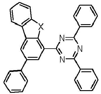

wherein in Compound C163: X=O, in Compound C164: X=S, in Compound C165: X=Se, wherein in Compound C166: X=O, in Compound C167: X=S, in Compound C168: X=Se, Compound C169 through C171, each represented by the formula Compound C172 through C174, each represented by the formula 

wherein in Compound C169: X=O, in Compound C170: X=S, in Compound C171: X=Se, wherein in Compound C172: X=O, in Compound C173: X=S, in Compound C174: X=Se, , Compound C175 through C177, each represented by the formula Compound C178 through C180, each represented by the formula 
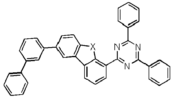
wherein in Compound C175: X=O, in Compound C176: X=S, in Compound C177: X=Se, wherein in Compound C178: X=O, in Compound C179: X=S, in Compound C180: X=Se, Compound C181 through C183, each represented by the formula Compound C184 through C186, each represented by the formula 

wherein in Compound C181: X=O, in Compound C182: X=S, in Compound C183: X=Se, wherein in Compound C184: X=O, in Compound C185: X=S, in Compound C186: X=Se, Compound C187 through C189, each represented by the formula Compound C190 through C192, each represented by the formula 

wherein in Compound C187: X=O, in Compound C188: X=S, in Compound C189: X=Se, wherein in Compound C190: X=O, in Compound C191: X=S, in Compound C192: X=Se, Compound C193 through C195, each represented by the formula Compound C196 through C198, each represented by the formula 

wherein in Compound C193: X=O, in Compound C194: X=S, in Compound C195: X=Se, wherein in Compound C196: X=O, in Compound C197: X=S, in Compound C198: X=Se, Compound C199 through C201, each represented by the formula Compound C202 through C204, each represented by the formula 

wherein in Compound C199: X=O, in Compound C200: X=S, in Compound C201: X=Se, wherein in Compound C202: X=O, in Compound C203: X=S, in Compound C204: X=Se, , Compound C205 through C207, each represented by the formula Compound C208 through C210, each represented by the formula 

wherein in Compound C205: X=O, in Compound C206: X=S, in Compound C207: X=Se, wherein in Compound C208: X=O, in Compound C209: X=S, in Compound C210: X=Se, Compound C211 through C213, each represented by the formula Compound C214 through C216, each represented by the formula 

wherein in Compound C211: X=O, in Compound C212: X=S, in Compound C213: X=Se, wherein in Compound C214: X=O, in Compound C215: X=S, in Compound C216: X=Se, Compound C217 through C219, each represented by the formula Compound C220 through C222, each represented by the formula 

wherein in Compound C217: X=O, in Compound C218: X=S, in Compound C219: X=Se, wherein in Compound C220: X=O, in Compound C221: X=S, in Compound C222: X=Se, Compound C223 through C225, each represented by the formula Compound C226 through C228, each represented by the formula 

wherein in Compound C223: X=O, in Compound C224: X=S, in Compound C225: X=Se, wherein in Compound C226: X=O in Compound C227: X=S, in Compound C228: X=Se, Compound C229 through C231, each represented by the formula Compound C232 through C234, each represented by the formula Compound C235 through C237, each represented by the formula 


wherein in Compound C229: X=O, in Compound C230: X=S, in Compound C231: X=Se, wherein in Compound C232: X=O, in Compound C233: X=S, in Compound C234: X=Se, wherein in Compound C235: X=O, in Compound C236: X=S, in Compound C237: X=Se, Compound C238 through C240, each represented by the formula Compound C241 through C243, each represented by the formula Compound C244 through C246, each represented by the formula 


wherein in Compound C238: X=O, in Compound C239: X=S, in Compound C240: X=Se, wherein in Compound C241: X=O, in Compound C242: X=S, in Compound C243: X=Se, wherein in Compound C244: X=O, in Compound C245: X=S, in Compound C246: X=Se, Compound C247 through C249, each represented by the formula Compound C250 through C252, each represented by the formula Compound C253 through C255, each represented by the formula 


wherein in Compound C247: X=O, in Compound C248: X=S, in Compound C249: X=Se, wherein in Compound C250: X=O, in Compound C251: X=S, in Compound C252: X=Se, wherein in Compound C253: X=O, in Compound C254: X=S, in Compound C255: X=Se, 

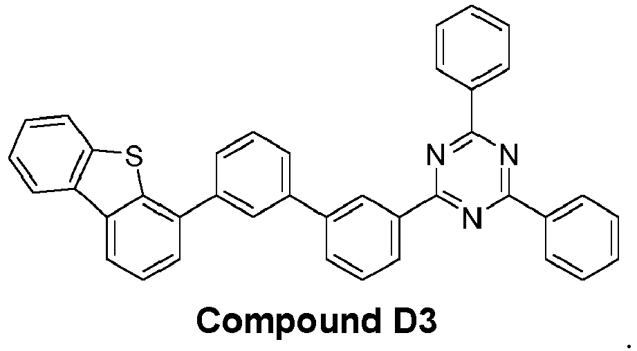
- The phosphorescent dopant may emit light from a triplet excited state to a ground singlet state in the device at room temperature. The phosphorescent dopant may be a metal coordination complex having a metal-carbon bond. The metal may be Ir, Os, Pt, Pd, Ag, Au, or Cu. The metal coordination complex may include a ligand having a chemical moiety of pyridazine, pyrimidine, pyrazine, and/or triazine. The metal coordination complex may have the formula of M(L1)x(L2)y(L3)z, whereL1, L2 and L3 may be the same or different, where x is 1, 2, or 3, where y is 0, 1, or 2, where z is 0, 1, or 2, where x+y+z is the oxidation state of the metal M, where L1, L2 and L3 may each independently selected from:


- The metal coordination complex may have the formula of Ir(LA)3, Ir(LA)(LB)2, Ir(LA)2(LB), Ir(LA)2(LC), or Ir(LA)(LB)(LC), where LA, LB, and LC are different from each other. The metal coordination complex may have a formula of Pt(LA)(LB), where LA, and LB can be same or different, and where LA, and LB may be optionally connected to form a tetradentate ligand.
- The metal coordination complex may have a formula of Ir(LA)2(LC), where LA is selected from:


- In some embodiments, the metal coordination complex may be selected from:


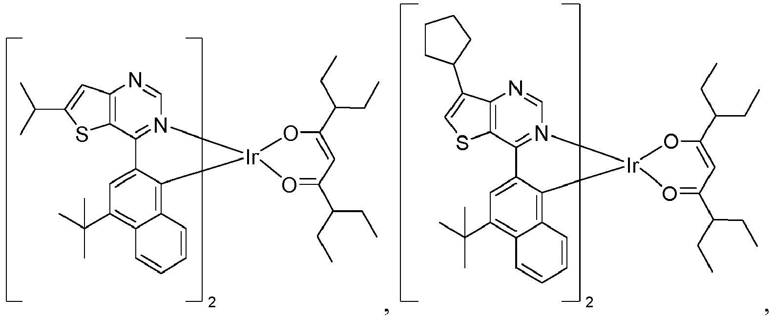


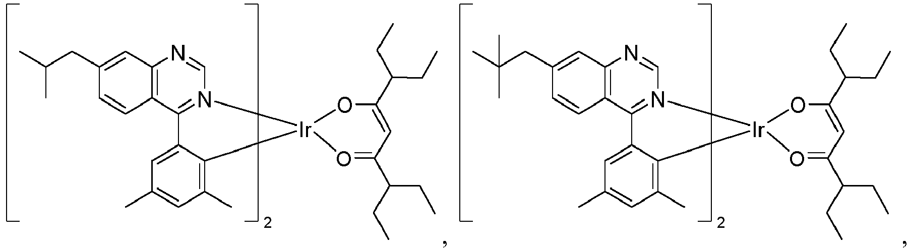

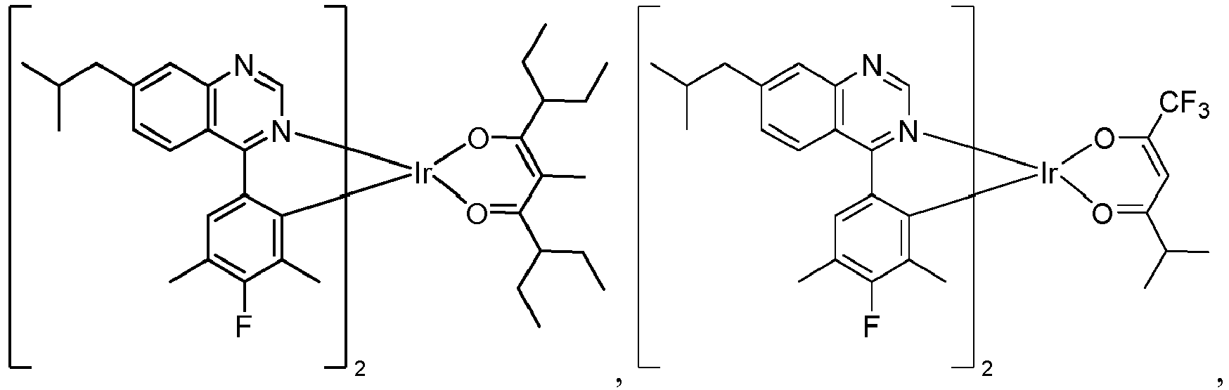


- The metal coordination complex may be a Pt complex having a tetradentate ligand. The tetradentate ligand may have four coordination atoms selected from: (two anionic C, two neutral N); (one anionic C, one carbene C, one neutral N, and one anionic N); (two anionic C, one carbene C, one neutral N); (one anionic C, one anionic N, two neutral N); (one anionic C, one anionic O, two neutral N); (two carbene C, two anionic N.
- The electron blocking layer may include the compound of Formula II:

- The electron blocking layer may include a compound selected from:
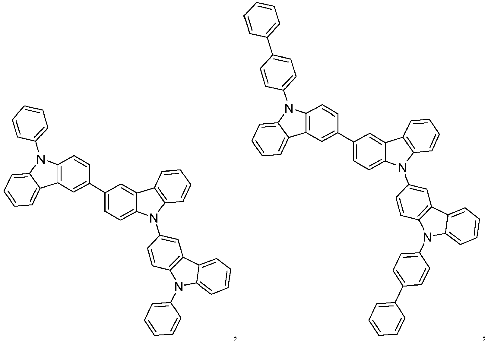


- In some embodiments, the OLED has one or more characteristics selected from the group consisting of being flexible, being rollable, being foldable, being stretchable, and being curved. In some embodiments, the OLED is transparent or semi-transparent. In some embodiments, the OLED further comprises a layer comprising carbon nanotubes.
- In some embodiments, the OLED further comprises a layer comprising a delayed fluorescent emitter. In some embodiments, the OLED comprises a RGB pixel arrangement or white plus color filter pixel arrangement. In some embodiments, the OLED is a mobile device, a hand held device, or a wearable device. In some embodiments, the OLED is a display panel having less than 10 inch diagonal or 50 square inch area. In some embodiments, the OLED is a display panel having at least 10 inch diagonal or 50 square inch area. In some embodiments, the OLED is a lighting panel.
- In some embodiments of the emissive region, the emissive region further comprises a host.
- In some embodiments, the compound can be an emissive dopant. In some embodiments, the compound can produce emissions via phosphorescence, fluorescence, thermally activated delayed fluorescence, i.e., TADF (also referred to as E-type delayed fluorescence), triplet-triplet annihilation, or combinations of these processes.
- The OLED disclosed herein can be incorporated into one or more of a consumer product, an electronic component module, and a lighting panel. The organic layer can be an emissive layer and the compound can be an emissive dopant in some embodiments, while the compound can be a non-emissive dopant in other embodiments.
- The organic layer can also include a host. In some embodiments, two or more hosts are preferred. In some embodiments, the hosts used maybe a) bipolar, b) electron transporting, c) hole transporting or d) wide band gap materials that play little role in charge transport. In some embodiments, the host can include a metal complex. The host can be an inorganic compound.
- The materials described herein as useful for a particular layer in an organic light emitting device may be used in combination with a wide variety of other materials present in the device. For example, emissive dopants disclosed herein may be used in conjunction with a wide variety of hosts, transport layers, blocking layers, injection layers, electrodes and other layers that may be present. The materials described or referred to below are non-limiting examples of materials that may be useful in combination with the compounds disclosed herein, and one of skill in the art can readily consult the literature to identify other materials that may be useful in combination.
- Various materials may be used for the various emissive and non-emissive layers and arrangements disclosed herein. Examples of suitable materials are disclosed in
U.S. Patent Application Publication No. 2017/0229663 , which is incorporated by reference in its entirety. - A charge transport layer can be doped with conductivity dopants to substantially alter its density of charge carriers, which will in turn alter its conductivity. The conductivity is increased by generating charge carriers in the matrix material, and depending on the type of dopant, a change in the Fermi level of the semiconductor may also be achieved. Hole-transporting layer can be doped by p-type conductivity dopants and n-type conductivity dopants are used in the electron-transporting layer.
- A hole injecting/transporting material to be used in the present invention is not particularly limited, and any compound may be used as long as the compound is typically used as a hole injecting/transporting material.
- An electron blocking layer (EBL) may be used to reduce the number of electrons and/or excitons that leave the emissive layer. The presence of such a blocking layer in a device may result in substantially higher efficiencies, and or longer lifetime, as compared to a similar device lacking a blocking layer. Also, a blocking layer may be used to confine emission to a desired region of an OLED. In some embodiments, the EBL material has a higher LUMO (closer to the vacuum level) and/or higher triplet energy than the emitter closest to the EBL interface. In some embodiments, the EBL material has a higher LUMO (closer to the vacuum level) and or higher triplet energy than one or more of the hosts closest to the EBL interface. In one aspect, the compound used in EBL contains the same molecule or the same functional groups used as one of the hosts described below.
- The light emitting layer of the organic EL device of the present invention preferably contains at least a metal complex as light emitting material, and may contain a host material using the metal complex as a dopant material. Examples of the host material are not particularly limited, and any metal complexes or organic compounds may be used as long as the triplet energy of the host is larger than that of the dopant. Any host material may be used with any dopant so long as the triplet criteria is satisfied.
- A hole blocking layer (HBL) may be used to reduce the number of holes and/or excitons that leave the emissive layer. The presence of such a blocking layer in a device may result in substantially higher efficiencies and/or longer lifetime as compared to a similar device lacking a blocking layer. Also, a blocking layer may be used to confine emission to a desired region of an OLED. In some embodiments, the HBL material has a lower HOMO (further from the vacuum level) and or higher triplet energy than the emitter closest to the HBL interface. In some embodiments, the HBL material has a lower HOMO (further from the vacuum level) and or higher triplet energy than one or more of the hosts closest to the HBL interface.
- An electron transport layer (ETL) may include a material capable of transporting electrons. The electron transport layer may be intrinsic (undoped), or doped. Doping may be used to enhance conductivity. Examples of the ETL material are not particularly limited, and any metal complexes or organic compounds may be used as long as they are typically used to transport electrons.
- In tandem or stacked OLEDs, the CGL plays an essential role in the performance, which is composed of an n-doped layer and a p-doped layer for injection of electrons and holes, respectively. Electrons and holes are supplied from the CGL and electrodes. The consumed electrons and holes in the CGL are refilled by the electrons and holes injected from the cathode and anode, respectively; then, the bipolar currents reach a steady state gradually. Typical CGL materials include n and p conductivity dopants used in the transport layers.
- Deep HOMO emitters may be PHOLED (phosphorescent organic light emitting diode) emitters with narrow spectrum, high LE / EQE (luminous efficacy/external quantum efficiency) ratio, long lifetime, and an EQE value above a predetermined amount. For example, the narrow spectrum of the deep HOMO emitters may have full width at half maximum (FHWM) values of less than 50 nm, less than 45 nm, less than 40 nm, or the like. Due to narrow electroluminescent (EL) spectrum, the amount of photon emitting in invisible range over 670 nm may be minimized compared to conventional broad red emitters, and thus less photons losses may occur. Most of the emitted photons may be in the visible range, which may provide for higher luminance efficiency at the same EQE for the narrow EL emitters.
- Many narrow EL emitters may have deeper HOMO levels (e.g., ∼ -5.3 eV) when compared to the HOMO levels for broad emitters (e.g., ∼ -5.1 eV). This may cause different behavior of the emitter in the device. Embodiments of the disclosed subject matter may provide a different approach for the efficient device structure architecture for deep HOMO emitters, such as for deep HOMO red emitters.
- Many families of deep HOMO emitters may have desirable PHOLED performance with narrow spectrum, high LE / EQE ratio, long lifetime, and potentially very high EQE. Due to narrow EL spectrum, the amount of photon emitting in invisible range over 670 nm may be minimized, compared to conventional broad red emitters and thus less photons losses occur. Most of the emitted photons may be in the visible range, so as to provide higher luminance efficiency at the same EQE for the narrow EL emitters.
- Many narrow EL emitters may have deeper HOMO level (e.g., ∼5.3 eV) when compared to the HOMO level for broad emitters (e.g., ∼5.1 eV). This may cause different behavior of the emitter in the device, and different device structure architecture for deep HOMO emitters may be used.
- In addition to narrow red emitters, there may be families of green emitters with desired performance and deep HOMO (e.g., >5.2 eV), and similar device structure architectures may be used.
- Embodiments of the disclosed subject matter provide designs for an efficient device structure for deep HOMO emitters. There may be differences in the device properties between the emitters RD1 and RD2 in the same device structure (e.g., as shown in
FIG. 6 and Table 2). The differences may be attributed to a recombination zone (RZ) location in the EML. A hole blocking layer (HBL) may affect the efficiency of deep HOMO RD1 emitter device, whereas an electron blocking layer (EBL) may not affect efficiency (e.g., as shown in examples 1, 2, 3, 4 of Table 2). For the emitter RD2, there may be no difference in device efficiency due to HBL, but there may be differences due to EBL (see, e.g., examples 5, 6, 7, 8 of Table 2). - The RD1 device may have a recombination zone close to the HBL side of EML (emissive layer). The HBL may improve RD1 device efficiency by preventing exciton quenching and electron leakage to the ETL (electron transport layer). For the same reason, the RD2 device may have a recombination zone (RZ) close to the EBL, and the EBL may improve device efficiency by prevention of exciton quenching and hole leakage to the HTL (hole transport layer). Deep HOMO RD1 may provide improved hole transport to the HBL side of EML, as there may be less hole trapping. In contrast, the reference shallow HOMO RD2 may not provide enough hole transport through the EML, as there may be more hole trapping. The RZ may be localized so as to be in the proximity of EBL.
- Embodiments of the disclosed subject matter may provide for the combination of the deep HOMO emitter and HBL to provide improved device efficiency. Efficiency roll off with luminance increase may be a problem for phosphorescent devices, and reduction of efficiency roll-off may be important in order to provide increased device efficiency at higher luminances. EQE roll off may be calculated as ratio of EQE at 10 mA/cm2 to EQE of 1 ma/cm2 for the same device (see, e.g., last column in Table 2). Data in Table 2 and
FIG. 6 shows that HBL may provide efficiency roll-off reduction for the RD1 deep HOMO emitter (see, e.g., Example 1 vs. Example 2 and Example 3 vs. Example 4 in Table 2) and may have no or minimal roll off effect on a device with an RD2 emitter (see, e.g., Example 6 vs. Example 5 and Example 7 vs. Example 8 in Table 2). - All example devices were fabricated by high vacuum (<10-7 Torr) thermal evaporation. The anode electrode was 1,150 Å of indium tin oxide (ITO). The cathode was comprised of 10 Å of Liq (8-hydroxyquinoline lithium) followed by 1,000 Å of Al. All devices were encapsulated with a glass lid sealed with an epoxy resin in a nitrogen glove box (<1 ppm of H2O and O2) immediately after fabrication, and a moisture getter was incorporated inside the package. The organic stack of the device examples sequentially included, from the ITO surface, 100Å of HAT-CN (Hexaazatriphenylenehexacarbonitrile) as the hole injection layer (HIL); 400 or 450 Å of HTM (hole transport material) as a hole transporting layer (HTL); 50Å of EBM (electron blocking material) (if any) as an electron blocking layer (EBL); 400 Å of an emissive layer (EML) containing from red host H1 and 3% of RD1 or RD2 red emitters, 50Å of HBM as hole blocking layer (HBL) (if any) and 300 (with HBL) or 350 Å (no HBL) of Liq (8-hydroxyquinoline lithium) doped with 35% of ETM as the ETL.
-
FIG. 3 shows a device structure according to an embodiments of the disclosed subject matter. The device may include a cathode, an electron ejection layer (EIL), an electron transport layer (ETL), an optional a hole blocking layer (HBL), an emissive layer (EML), an optional electron blocking layer (EBL), a hole transport layer (HTL) a hole injection layer (HIL), and an anode. - When not including the using EBL, the HTL thickness was 50Å thicker, and when the HBL is not includes, the ETL thickness was 50Å thicker, so total device thickness remained the same to prevent possible device performance distortion due to different layer thicknesses.
- Table 1 shows the device layer thickness and materials. The chemical structures of the device materials are shown in
FIG. 4 .Table 1. Device layer materials and thicknesses Layer Material Thickness [Å] Anode ITO 1,150 HIL HAT- CN 100 HTL HTM 400-450 EBL EBM 50 (if any) EML Host: RD 3%400 HBL HBM 50 (if any) ETL Liq: ETM 35% 300-350 EIL Liq 10 Cathode A1 1000 - Upon fabrication, the devices have been EL and JVL (current density, voltage, luminance) tested. The device performance data are summarized in Table 2.
Table 2. Device structures and performance of the device examples with various red emitters and blocking layers. Device Example EBL Host Emitter 3% HBL 1931 CIE At 1mA/cm2 At 10mA/cm2 EQE roll-off x y Voltage [v] LE [cd/A] EQE [%] Voltage [v] LE [cd/A] EQE [%] 10/1 mA/cm2 Example 1 EBM Host 1 RD1 HBM 0.686 0.313 2.9 23.5 24.7 3.8 20.8 21.8 0.89 Example 2 EBM Host 1 RD1 0.686 0.313 2.8 21.6 22.7 3.7 18.0 18.9 0.83 Example 3 Host 1RD1 HBM 0.686 0.313 2.9 23.4 24.6 3.8 20.7 21.7 0.88 Example 4 Host 1RD1 0.686 0.313 2.8 21.7 22.7 3.7 17.9 18.8 0.83 Example 5 EBM Host 1 RD2 HBM 0.683 0.316 3.1 23.2 27.1 4.3 21.0 24.5 0.90 Example 6 EBM Host 1 RD2 0.683 0.316 3.0 23.2 27.0 4.1 21.0 24.4 0.90 Example 7 Host 1RD2 HBM 0.683 0.317 3.0 22.5 26.1 4.2 20.0 23.2 0.89 Example 8 Host 1RD2 0.682 0.317 2.9 22.7 26.3 4.1 20.1 23.2 0.88 - To understand the device performance, HOMO-LUMO and T1 energy levels of the materials have been used. HOMO and LUMO Energy Levels were determined by solution cyclic voltammetry and differential pulsed voltammetry. Measurements were performed using a CH Instruments model 6201B potentiostat using anhydrous dimethylformamide solvent and tetrabutylammonium hexafluorophosphate as the supporting electrolyte. Glassy carbon, and platinum and silver wires were used as the working, counter and reference electrodes, respectively. Electrochemical potentials were referenced to an internal ferrocene-ferroceniumredox couple (Fc/Fc+) by measuring the peak potential differences from differential pulsed voltammetry. The corresponding highest occupied molecular orbital (HOMO) energy and the lowest unoccupied molecular orbital (LUMO) energy were determined by referencing the cationic and anionic redox potentials to ferrocene (4.8 eV vs. vacuum). That is:


- To determine the T1 level, less than 1mg of material was dissolved by ultrasonication in 2 mL of 2-methyltetrahydrofuran solvent. The solution was filtered through a 2 micron filter into a quartz tube. The tube was sealed with a rubber septum and bubble degassed with nitrogen in order to prevent oxygen quenching. The phosphorescence spectrum was carried out on a Horiba Jobin Yvon Fluorolog-3 system equipped with a xenon lamp at low temperature close to 77 K. The T1 is determined using PL at 77K. That is:

- HOMO-LUMO and T1 levels are listed in Table 3 below, and
FIG. 5 shows the HOMO-LUMO levels of a device materials according to embodiments of the disclosed subject matter.Table 3. Energy levels and T1 for the materials used in the device examples Material HOMO [eV] LUMO [eV] T1 [nm] ITO 4.70 HAT-CN 9.70 4.20 HTM 5.16 1.85 523 EBM 5.38 1.84 452 Host 15.43 2.88 516 RD1 5.32 2.81 614 RD2 5.05 2.49 606 HBM 5.96 2.74 484 ETM 5.64 2.71 706 Host 25.96 2.74 484 Host 35.11 2.37 536 HBL 15.90 2.90 569 HBL 25.64 2.73 454 HBL 35.70 2.47 420 - The calculated energy levels for HBM are shown below, and may have similarities to compound H:

DFT (Density Functional Theory) T1 421 S1 370 Gap 3.804 HOMO -5.795 LUMO -1.991 - There may be differences in the device properties between emitter RD1 and RD2 in the same device structure (see, e.g.,
FIG. 6 and Table 2), and may be based on the recombination zone (RZ) location in the EML. The HBL may affect the efficiency of deep HOMO RD1 emitter device, whereas the EBL may not affect efficiency (see, e.g., Examples 1, 2, 3, 4 in Table 2). - In contrast, with reference emitter RD2, there may be no difference in device efficiency due to HBL, but there may be a difference due to EBL (see, e.g., examples 5, 6, 7, 8 shown in Table 2). The RD1 device may have a recombination zone close to the HBL side of EML, and the HBL may improve RD1 device efficiency by preventing exciton quenching and electron leakage to the ETL. When the RD2 device may have recombination zone RZ close to EBL, and the EBL may improve device efficiency by prevention of exciton quenching and hole leakage to the HTL.
- Deep HOMO RD1 may exhibit less hole trapping and/or improved hole transport, which may provide a higher exciton population near the cathode side of the EML. In contrast, reference shallow HOMO RD2 may hole trap more strongly and/or hole transport less through the EML, which may provide a RZ localized in the proximity of EBL. In embodiments of the disclosed subject matter, the combination of deep HOMO emitter and HBL may provide the desired device efficiency.
- Efficiency roll off with luminance increase may be a problem for phosphorescent devices. Reduction of efficiency roll-off may provide a higher device efficiency at a higher luminance. EQE roll off was calculated as ratio of EQE at 10 mA/cm2 to EQE of 1 mA/cm2 for the same device (see, e.g., the last column in the Table 2). Data in Table 2 and
FIG. 6 show that HBL provides efficiency roll-off reduction for the RD1 deep HOMO emitter (see, e.g., Example 1 vs. Example 2 and Example 3 vs. Example 4 in Table 2) and has no or minimal roll off effect on device with RD2 emitter (see, e.g., Example 6 vs. Example 5 and Example 7 vs. Example 8 shown in Table 2). - The hole transporting layer (HTM) may have good hole transporting properties (e.g., HOMO 5.16 eV). The electron blocking layer (EBL) may have a shallow LUMO level (e.g., 1.84 eV) to prevent electron leakage to HTL and high T1 energy (e.g., 452 nm) enough to prevent any exciton leakage from EML into HTL and reasonable hole transporting properties (e.g., HOMO 5.38 eV).
- In embodiments of the disclosed subject matter, EBL T1 may be higher than T1 of the emitter. Host (Host 1) may provide electron transport through the EML (e.g., LUMO 2.88 eV), as well as hole transport (e.g., HOMO 5.43 eV), in the absence of emitters with shallower HOMO levels. Embodiments of the disclosed subject matter may include one or more hosts (e.g., single host dual host, or the like).
- Shallow HOMO emitters e.g., RD2 - (HOMO 5.05 eV), may provide more hole trap and deep HOMO emitters e.g. RD1 (HOMO 5.32 eV) may provide more hole transport through the EML. This may shift the recombination zone in the EML depending on the emitter. In case with deep HOMO emitters, the recombination zone may be shifted toward HBL. The HBL effect on the device efficiency may be more pronounced with RD1 deep HOMO emitter. RD2 may provide more hole trapping, resulting in less hole transport through the EML, so RZ may be shifted toward the EBL interface. The EBL may affect the efficiency of the RD2 emitter device.
- The HOMO for deep HOMO emitters may be in the range of 5.1 - 5.6 eV, more preferable 5.15 - 5.55 eV, even more preferable 5.2 - 5.5 eV.
- Hole trapping may be a function of the emitter-host HOMO energy gap. The HBL for emitter-host energy gap may be less than 0.15 eV. The hole blocking material (HBM) may have a deep HOMO (5.96 eV), which may block holes from leaking into ETL, and may have high T1 energy (e.g., 484 nm) to prevent exciton leakage into ETL. In embodiments of the disclosed subject matter, the HBL may have a HOMO level deeper than 5.5 eV.
- The ETM may provide electron transport through the ETL toward the EML (e.g., LUMO 2.71 eV).
- The combination of the deep HOMO emitter R1 and the HBL in the devices and/or structures of the disclosed subject matter may provide increased efficiency, minimal efficiency roll off, and increased power efficiency.
- Embodiments of the disclosed subject matter may provide the following types of red emitters with deep HOMO:

- Embodiments of the disclosed subject matter may provide deep HOMO red ligand structures for emissive ligand:


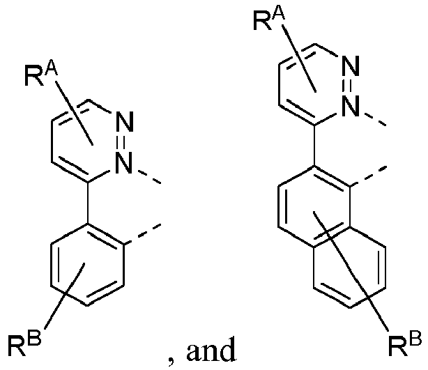

- In some embodiments, the OLED may include at least one emitter selected from the group of emitters shown below.


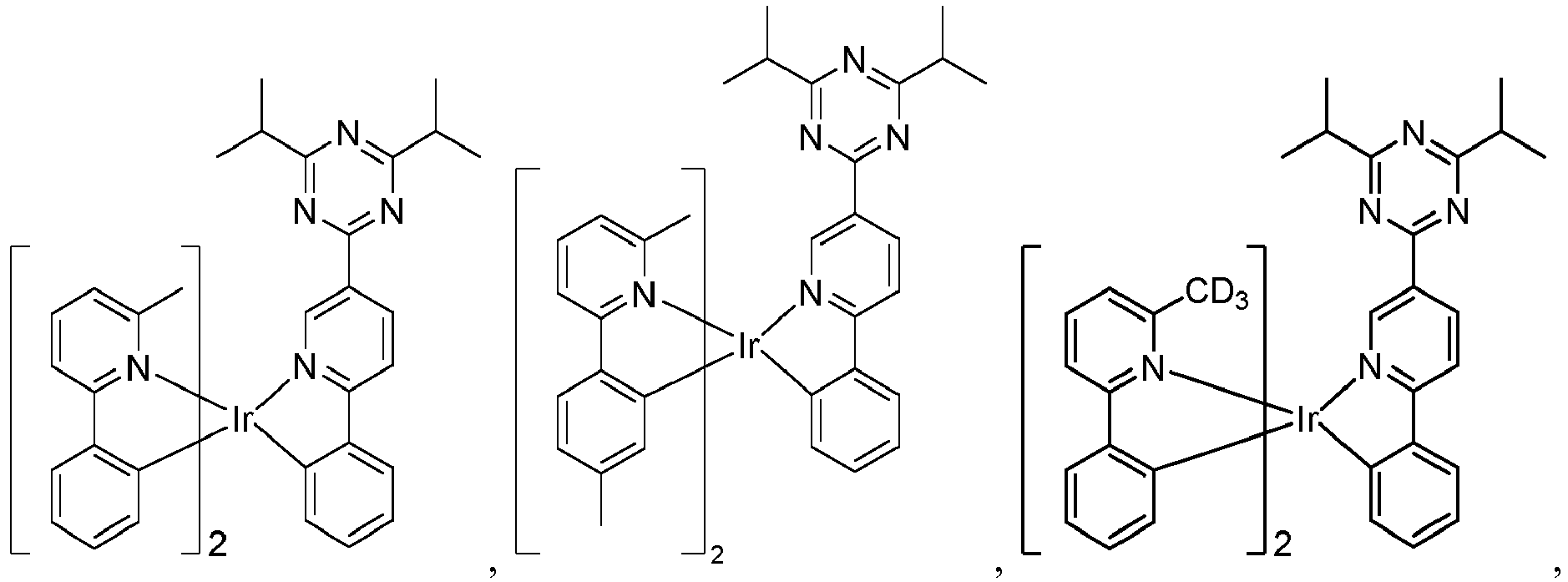

- Additional device data was obtained to show the blocking layer material and hosts classes of the compounds that may provide improvement of the performance of deep HOMO red emitter devices with a blocking layer. Two hosts,
single Host 1 and dual Host 2 : Host 3 (4:1), and three blocking layer materials (e.g., HBL1, HBL2, HBL3) were used in the devices with deep HOMO emitter RD1 and shallow HOMO emitter RD2. Both emitters have approximately same color saturation, but different type of energy levels. - The device fabrication is the same as described above, and
FIG. 7 shows device materials according to embodiments of the disclosed subject matter. - Experimental data are summarized below in Table 4, which shows the correlation of the device EQE and the blocking layer in the device.
Table 4. Device performance of additional experiments. HBL effect on EQE of deep HOMO red emitter structures. Device Example EBL Host Emitter 3% HBL 1931 CIE EQE at 10 mA/cm2 [%] x y Example 9 EBM Host 1 RD1 HBL1 0.685 0.315 20.1 Example 10 EBM Host 1 RD1 HBL2 0.685 0.315 20.1 Example 11 EBM Host 1 RD1 HBL3 0.684 0.315 19.5 Example 12 EBM Host 1 RD1 0.685 0.314 18.2 Example 13 EBM Host 2: Host 3 (4:1) RD1 HBL1 0.674 0.325 23.7 Example 14 EBM Host 2: Host 3 (4:1) RD1 HBL2 0.673 0.326 24.3 Example 15 EBM Host 2: Host 3 (4:1) RD1 HBL3 0.673 0.326 24.1 Example 16 EBM Host 2: Host 3 (4:1) RD1 0.674 0.325 22.2 Example 17 EBM Host 1 RD2 HBL1 0.683 0.316 24.0 Example 18 EBM Host 1 RD2 HBL2 0.683 0.316 23.5 Example 19 EBM Host 1 RD2 HBL3 0.683 0.316 24.1 Example 20 EBM Host 1 RD2 0.683 0.316 24.0 Example 21 EBM Host 2: Host 3 (4:1) RD2 HBL1 0.671 0.328 24.8 Example 22 EBM Host 2: Host 3 (4:1) RD2 HBL2 0.672 0.327 25.4 Example 23 EBM Host 2: Host 3 (4:1) RD2 HBL3 0.672 0.327 25.2 Example 24 EBM Host 2: Host 3 (4:1) RD2 0.669 0.330 24.9 - The EQE of the devices with deep HOMO RD1 emitter may be affected by a BL (blocking layer), which may be about 10% higher, versus the EQE of a device without a BL. For a single host, as shown in examples 9, 10, and 11, the EQE with the blocking layer structures may be about 20%. In contrast, Example 12 shows that reference structure without a BL may have an EQE about 18%.
- Dual host devices with the RD1 deep HOMO emitter may be similarly affected by the BL. In examples 13, 14, and 15, the BL structures have an EQE about 24%. In example 16, devices with no BL structures may have an EQE ∼22 %.
- The EQE of the device with the RD2 shallow HOMO emitter may not be affected by HBL. In single host examples 17, 18, and 19, BL devices may have similar EQE to the EQE of devices without the BL (e.g., Example 20, where the EQE is about 24%). The EQE of the dual host devices including BL, such as in examples 21, 22, and 23, may be similar to the EQE of the devices without the BL of Example 24 (e.g., about 25%).
- Different classes of BL materials may be used with the HOMO emitters. Examples BL1, BL2, BL3, and/or HBM may belong to the following classes of the materials: Aluminum Quinoline complexes, Aza-dibenzothiopene derivatives, Indolo[2,3-a] carbazole derivatives, 4,6- disubstituted Dibenzothiophenes. These different classes may work as BL materials for deep HOMO red emitter PHOLED devices.
- The energy levels of additional hosts and blocking layers are shown above in Table 3. Table 3 shows the energy levels of all the materials used in the device examples.
- It is understood that the various embodiments described herein are by way of example only, and are not intended to limit the scope of the invention. For example, many of the materials and structures described herein may be substituted with other materials and structures without deviating from the spirit of the invention. The present invention as claimed may therefore include variations from the particular examples and preferred embodiments described herein, as will be apparent to one of skill in the art. It is understood that various theories as to why the invention works are not intended to be limiting.
- The invention is further described by the following numbered paragraphs:
- 1. An organic light emitting diode (OLED) comprising:
- an anode; a cathode; an emissive layer disposed between the anode and the cathode; and
- a hole blocking layer disposed between the emissive and the cathode,
- wherein the emissive layer comprises a phosphorescent dopant,
- wherein the phosphorescent dopant has an emission in 0.5% doped PMMA (Poly(methyl methacrylate)) thin film with a peak maximum wavelength that is greater than or equal to 600 nm at room temperature, wherein the energy of a highest occupied molecular orbital (HOMO) of the phosphorescent dopant is lower than or equal to -5.1 eV, and wherein the energy of the HOMO of the hole blocking layer is at least 0.1 eV lower than the energy of the HOMO of the phosphorescent dopant.
- 2. The OLED of
paragraph 1, wherein the peak maximum wavelength of the phosphorescent dopant is selected from the group consisting of: greater than or equal to 610 nm, greater than or equal to 620 nm, greater than or equal to 630 nm, greater than or equal to 650 nm, greater than or equal to 700 nm, greater than or equal to 750 nm, and greater than or equal to 800 nm. - 3. The OLED of
paragraph 1, wherein the hole blocking layer is disposed on the emissive layer. - 4. The OLED of
paragraph 1, wherein the energy of the HOMO of the phosphorescent dopant is selected from the group consisting of: lower than or equal to -5.2 eV, lower than or equal to -5.3 eV, and lower than or equal to -5.4 eV. - 5. The OLED of
paragraph 1, wherein the energy of the HOMO of the hole blocking layer is selected from the group consisting of: at least 0.2 eV lower than the energy of the HOMO of the phosphorescent dopant, at least 0.3 eV lower than the energy of the HOMO of the phosphorescent dopant, and at least 0.4 eV lower than the energy of the HOMO of the phosphorescent dopant. - 6. The OLED of
paragraph 1, wherein the hole blocking layer comprises a compound of Formula I, which is at least one selected from the group consisting of:

- 7. The OLED of
paragraph 6, wherein each R1, R2 and R3 is independently a hydrogen or a substituent selected from the group consisting of: aryl, heteroaryl, and combinations thereof. - 8. The OLED of
paragraph 6, wherein each X is independently selected from N, or CH, and/or Y is selected from the group consisting of O, S, and N Ar4. - 9. The OLED of
paragraph 6, wherein the compound of Formula I is the only compound in the hole blocking layer. - 10. The OLED of
paragraph 6, wherein the compound of Formula I is at least one selected from the group consisting of:
- 11. The OLED of
paragraph 6, wherein the compound of Formula I is at least one selected from the group consisting of Compounds A1 to A117, B1 to B8, C1 to C255, andD 1 to D3 as described herein before. - 12. The OLED of
paragraph 1, wherein the phosphorescent dopant emits light from a triplet excited state to a ground singlet state in the device at room temperature. - 13. The OLED of
paragraph 1, wherein the phosphorescent dopant is a metal coordination complex having a metal-carbon bond. - 14. The OLED of paragraph 13, wherein the metal is selected from the group consisting of: Ir, Os, Pt, Pd, Ag, Au, and Cu.
- 15. The OLED of
paragraph 14, wherein the metal is Ir. - 16. The OLED of
paragraph 14, wherein the metal is Pt. - 17. The OLED of paragraph 13, wherein the metal coordination complex comprises a ligand comprising a chemical moiety selected from the group consisting of: pyridazine, pyrimidine, pyrazine, and triazine.
- 18. The OLED of paragraph 13, wherein the metal coordination complex has the formula of M(L1)x(L2)y(L3)z, wherein L1, L2 and L3 can be the same or different, wherein x is 1, 2, or 3, wherein y is 0, 1, or 2, wherein z is 0, 1, or 2, wherein x+y+z is the oxidation state of the metal M, wherein L1, L2 and L3 are each independently selected from the group consisting of:


- 19. The OLED of
paragraph 18, wherein the metal coordination complex has a formula selected from the group consisting of: Ir(LA)3, Ir(LA)(LB)2, Ir(LA)2(LB), Ir(LA)2(LC), and Ir(LA)(LB)(LC); wherein LA, LB, and LC are different from each other. - 20. The OLED of
paragraph 18, wherein the metal coordination complex has a formula of Pt(LA)(LB), wherein LA, and LB can be same or different, and wherein LA, and LB are optionally connected to form a tetradentate ligand. - 21. The OLED of paragraph 19, wherein the metal coordination complex has a formula of Ir(LA)2(LC), wherein LA is selected from the group consisting of:


- 22. The OLED of paragraph 21, wherein the metal coordination complex is at least one selected from the group consisting of:


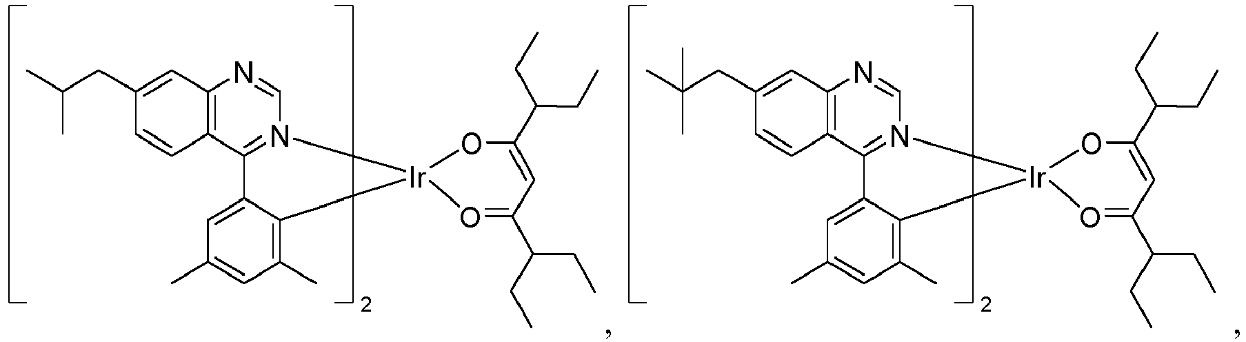


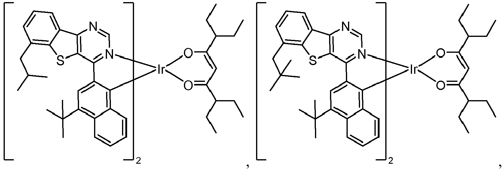


- 23. The OLED of
paragraph 20, wherein the metal coordination complex is a Pt complex having a tetradentate ligand. - 24. The OLED of paragraph 23, wherein the tetradentate ligand has four coordination atoms selected from the group consisting of: (two anionic C, two neutral N); (one anionic C, one carbene C, one neutral N, and one anionic N); (two anionic C, one carbene C, one neutral N); (one anionic C, one anionic N, two neutral N); (one anionic C, one anionic O, two neutral N); and (two carbene C, two anionic N).
- 25. The OLED of
paragraph 1, wherein the electron blocking layer comprises a compound of Formula II:
- 26. The OLED of paragraph 25, each R3, R4, and R5 is independently a hydrogen or a substituent selected from the group consisting of aryl, heteroaryl, and combination thereof.
- 27. The OLED of paragraph 25, wherein the electron blocking layer comprises a compound selected from the group consisting of:


- 28. The OLED of
paragraph 1, wherein the device is at least one type selected from the group consisting of: a flat panel display, a computer monitor, a medical monitor, a television, a billboard, a light for interior or exterior illumination and/or signaling, a heads-up display, a fully or partially transparent display, a flexible display, a laser printer, a telephone, a mobile phone, a tablet, a phablet, a personal digital assistant (PDA), a wearable device, a laptop computer, a digital camera, a camcorder, a viewfinder, a micro-display having an active area with a primary diagonal of 2 inches or less, a 3-D display, a virtual reality or augmented reality display, a vehicle, a video wall comprising multiple displays tiled together, a theater or stadium screen, and a sign.
Claims (15)
- An organic light emitting diode (OLED) comprising:an anode;a cathode;an emissive layer disposed between the anode and the cathode; anda hole blocking layer disposed between the emissive and the cathode,wherein the emissive layer comprises a phosphorescent dopant,wherein the phosphorescent dopant has an emission in 0.5% doped PMMA (Poly(methyl methacrylate)) thin film with a peak maximum wavelength that is greater than or equal to 600 nm at room temperature,wherein the energy of a highest occupied molecular orbital (HOMO) of the phosphorescent dopant is lower than or equal to -5.1 eV, andwherein the energy of the HOMO of the hole blocking layer is at least 0.1 eV lower than the energy of the HOMO of the phosphorescent dopant.
- The OLED of claim 1 or 2, wherein the peak maximum wavelength of the phosphorescent dopant is selected from the group consisting of: greater than or equal to 610 nm, greater than or equal to 620 nm, greater than or equal to 630 nm, greater than or equal to 650 nm, greater than or equal to 700 nm, greater than or equal to 750 nm, and greater than or equal to 800 nm.
- The OLED of claim 1, wherein the energy of the HOMO of the phosphorescent dopant is selected from the group consisting of: lower than or equal to -5.2 eV, lower than or equal to -5.3 eV, and lower than or equal to -5.4 eV.
- The OLED of any one of claims 1 to 3, wherein the energy of the HOMO of the hole blocking layer is selected from the group consisting of: at least 0.2 eV lower than the energy of the HOMO of the phosphorescent dopant, at least 0.3 eV lower than the energy of the HOMO of the phosphorescent dopant, and at least 0.4 eV lower than the energy of the HOMO of the phosphorescent dopant.
- The OLED of any one of claims 1 to 4, wherein the hole blocking layer comprises a compound of Formula I, which is at least one selected from the group consisting of:


 wherein R1, R2 and R3 each independently represent mono to the maximum allowable substitution, or no substitution,wherein each R1, R2 and R3 is independently a hydrogen or a substituent selected from the group consisting of: deuterium, halogen, alkyl, cycloalkyl, heteroalkyl, heterocycloalkyl, arylalkyl, alkoxy, aryloxy, amino, silyl, alkenyl, cycloalkenyl, heteroalkenyl, alkynyl, aryl, heteroaryl, acyl, carboxylic acid, ether, ester, nitrile, isonitrile, sulfanyl, sulfinyl, sulfonyl, phosphino, and combinations thereof,wherein each X is independently selected from the group consisting of N, CH, or CR3,wherein Y is selected from the group consisting of: O, S, Se, NAr4, CAr4Ar5, SiAr4Ar5, Fluorene (C-Ar1Ar2), and Silicon (Si-Ar1Ar2), and wherein Ar1 and Ar2 are the same or different aryl groups,wherein each Ar1-Ar5 is independently selected from the group consisting of: aryl, heteroaryl, and a combination thereof, andwherein L is a direct bond or a linker comprising at least one aromatic ring.
 - The OLED of claim 5, wherein each X is independently selected from the group consisting of N, or CH, and/or Y is selected from the group consisting of O, S, and NAr4.
- The OLED of any one of claims 1 to 6, wherein the phosphorescent dopant is a metal coordination complex having a metal-carbon bond.
- The OLED of claim 7, wherein the metal is selected from the group consisting of: Ir, Os, Pt, Pd, Ag, Au, and Cu.
- The OLED of claim 7 or 8, wherein the metal coordination complex comprises a ligand comprising a chemical moiety selected from the group consisting of: pyridazine, pyrimidine, pyrazine, and triazine.
- The OLED of any one of claims 7 to 9, wherein the metal coordination complex has the formula of M(L1)x(L2)y(L3)z,wherein L1, L2 and L3 can be the same or different,wherein x is 1, 2, or 3,wherein y is 0, 1, or 2,wherein z is 0, 1, or 2,wherein x+y+z is the oxidation state of the metal M,wherein L1, L2 and L3 are each independently selected from the group consisting of:


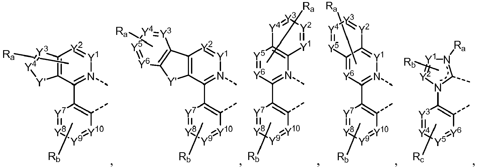

 wherein L2 and L3 can also be
 wherein each Y1 to Y13 are independently selected from the group consisting of carbon and nitrogen,wherein Y' is selected from the group consisting of B Re, N Re, P Re, O, S, Se, C=O, S=O, SO2, CReRf, SiReRf, and GeReRf;wherein Re and Rf are optionally fused or joined to form a ring,
wherein each Ra, Rb, Rc, and Rd may independently represent from mono substitution to the maximum possible number of substitution, or no substitution,wherein each Ra, Rb, Rc, Rd, Re and Rf is independently selected from the group consisting of hydrogen, deuterium, halogen, alkyl, cycloalkyl, heteroalkyl, heterocycloalkyl, arylalkyl, alkoxy, aryloxy, amino, silyl, alkenyl, cycloalkenyl, heteroalkenyl, alkynyl, aryl, heteroaryl, acyl, carboxylic acid, ether, ester, nitrile, isonitrile, sulfanyl, sulfinyl, sulfonyl, phosphino, and combinations thereof, andwherein any two adjacent substituents of Ra, Rb, Rc, and Rd are optionally fused or joined to form a ring or form a multidentate ligand. - The OLED of claim 10, wherein the metal coordination complex has a formula selected from the group consisting of: Ir(LA)3, Ir(LA)(LB)2, Ir(LA)2(LB), Ir(LA)2(LC), and Ir(LA)(LB)(LC); wherein LA, LB, and LC are different from each other.
- The OLED of claim 10, wherein the metal coordination complex has a formula of Pt(LA)(LB),wherein LA, and LB can be same or different, andwherein LA, and LB are optionally connected to form a tetradentate ligand.
- The OLED of claim 11, wherein the metal coordination complex has a formula of Ir(LA)2(LC),wherein LA is selected from the group consisting of:
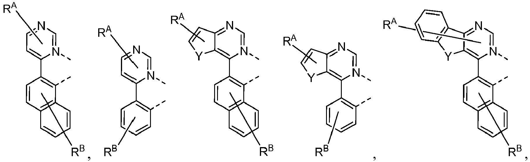


 wherein each RA, and RB may independently represent from mono substitution to the maximum possible number of substitution, or no substitution,wherein each RA, and RB is independently selected from the group consisting of:
hydrogen, deuterium, halogen, alkyl, cycloalkyl, heteroalkyl, heterocycloalkyl, arylalkyl, alkoxy, aryloxy, amino, silyl, alkenyl, cycloalkenyl, heteroalkenyl, alkynyl, aryl, heteroaryl, acyl, carboxylic acid, ether, ester, nitrile, isonitrile, sulfanyl, sulfinyl, sulfonyl, phosphino, and combinations thereof, andwherein any two adjacent substituents of RA, and RB are optionally fused or joined to form a ring or form a multidentate ligand. - The OLED of any one of the previous claims, wherein the electron blocking layer comprises a compound of Formula II:
 wherein R3, R4, and R5 each independently represent mono to the maximum allowable substitution, or no substitution,wherein each R3, R4, and R5 is independently a hydrogen or a substituent selected from the group consisting of deuterium, halogen, alkyl, cycloalkyl, heteroalkyl, heterocycloalkyl, arylalkyl, alkoxy, aryloxy, amino, silyl, alkenyl, cycloalkenyl, heteroalkenyl, alkynyl, aryl, heteroaryl, acyl, carboxylic acid, ether, ester, nitrile, isonitrile, sulfanyl, sulfinyl, sulfonyl, phosphino, and combinations thereof, andwherein each Ar5 and Ar6 is independently selected from the group consisting of aryl, heteroaryl, and combination thereof.
 - A consumer product including an organic light emitting device (OLED) of any one of the previous claims, comprising:an anode;a cathode;an emissive layer disposed between the anode and the cathode; anda hole blocking layer disposed between the emissive and the cathode,wherein the emissive layer comprises a phosphorescent dopant,wherein the phosphorescent dopant has an emission in 0.5% doped PMMA (Poly(methyl methacrylate)) thin film with a peak maximum wavelength that is greater than or equal to 600 nm at room temperature,wherein the energy of a highest occupied molecular orbital (HOMO) of the phosphorescent dopant is lower than or equal to -5.1 eV,wherein the energy of the HOMO of the hole blocking layer is at least 0.1 eV lower than the energy of the HOMO of the phosphorescent dopant.
Applications Claiming Priority (2)
| Application Number | Priority Date | Filing Date | Title |
|---|---|---|---|
| US201862749290P | 2018-10-23 | 2018-10-23 | |
| US16/596,948 US11515482B2 (en) | 2018-10-23 | 2019-10-09 | Deep HOMO (highest occupied molecular orbital) emitter device structures |
Publications (1)
| Publication Number | Publication Date |
|---|---|
| EP3644384A1 true EP3644384A1 (en) | 2020-04-29 |
Family
ID=68296227
Family Applications (1)
| Application Number | Title | Priority Date | Filing Date |
|---|---|---|---|
| EP19204284.4A Pending EP3644384A1 (en) | 2018-10-23 | 2019-10-21 | Deep homo (highest occupied molecular orbital) emitter device structures |
Country Status (5)
| Country | Link |
|---|---|
| US (2) | US11515482B2 (en) |
| EP (1) | EP3644384A1 (en) |
| JP (2) | JP7381286B2 (en) |
| KR (2) | KR102755178B1 (en) |
| CN (3) | CN111092164B (en) |
Cited By (3)
| Publication number | Priority date | Publication date | Assignee | Title |
|---|---|---|---|---|
| EP3909964A3 (en) * | 2020-05-14 | 2022-02-16 | Samsung Electronics Co., Ltd. | Organometallic compound, organic light-emitting device including the same, and electronic apparatus including the organic light-emitting device |
| US12152042B2 (en) | 2020-05-14 | 2024-11-26 | Samsung Electronics Co., Ltd. | Organometallic compound, organic light-emitting device including the same, and electronic apparatus including the organic light-emitting device |
| US12630574B2 (en) | 2021-05-07 | 2026-05-19 | Samsung Display Co., Ltd. | Organometallic compound, organic light-emitting device including the same, and electronic apparatus including the organic light-emitting device |
Families Citing this family (20)
| Publication number | Priority date | Publication date | Assignee | Title |
|---|---|---|---|---|
| US11217762B2 (en) * | 2018-11-30 | 2022-01-04 | Universal Display Corporation | Surface-plasmon-pumped light emitting devices |
| WO2021033724A1 (en) | 2019-08-19 | 2021-02-25 | 出光興産株式会社 | Compound, material for organic electroluminescent element, organic electroluminescent element, and electronic device |
| US11925105B2 (en) * | 2019-08-26 | 2024-03-05 | Universal Display Corporation | Organic electroluminescent materials and devices |
| KR20210050326A (en) * | 2019-10-28 | 2021-05-07 | 삼성전자주식회사 | Organometallic compound, organic light emitting device including the same and a composition for diagnosing including the same |
| CN111799385A (en) * | 2020-07-21 | 2020-10-20 | 京东方科技集团股份有限公司 | Organic light-emitting diode device and preparation method thereof, display substrate, and display device |
| CN111864095B (en) | 2020-07-23 | 2023-04-28 | 京东方科技集团股份有限公司 | Organic light-emitting diode structure and display device |
| US12543492B2 (en) | 2020-09-09 | 2026-02-03 | Universal Display Corporation | Organic electroluminescent materials and devices |
| US12369488B2 (en) | 2020-09-09 | 2025-07-22 | Universal Display Corporation | Organic electroluminescent materials and devices |
| US12588352B2 (en) | 2020-10-20 | 2026-03-24 | Universal Display Corporation | Energy levels and device structures for plasmonic OLEDs |
| WO2022082764A1 (en) * | 2020-10-23 | 2022-04-28 | 京东方科技集团股份有限公司 | Organic electroluminescent device and display device |
| CN114957205A (en) | 2021-02-22 | 2022-08-30 | 罗门哈斯电子材料韩国有限公司 | Organic electroluminescent compounds, various host materials and organic electroluminescent device comprising the same |
| WO2022177398A1 (en) * | 2021-02-22 | 2022-08-25 | 주식회사 엘지화학 | Novel compound and organic light-emitting device comprising same |
| KR102908391B1 (en) * | 2021-02-22 | 2026-01-07 | 주식회사 엘지화학 | Novel compound and organic light emitting device comprising the same |
| US20240228470A1 (en) * | 2021-04-14 | 2024-07-11 | P&H Tech Co., Ltd | Organic Compound And Organic Light Emitting Device Including Same |
| US12473317B2 (en) | 2021-06-04 | 2025-11-18 | Universal Display Corporation | Organic electroluminescent materials and devices |
| CN116156984A (en) * | 2021-11-13 | 2023-05-23 | 北京夏禾科技有限公司 | An organic electroluminescent device |
| WO2024170609A1 (en) | 2023-02-17 | 2024-08-22 | Merck Patent Gmbh | Materials for organic electroluminescent devices |
| WO2025210013A1 (en) | 2024-04-04 | 2025-10-09 | Merck Patent Gmbh | Compounds for electronic devices, in particular compounds for oleds |
| WO2026017611A1 (en) | 2024-07-15 | 2026-01-22 | Merck Patent Gmbh | Organic light emitting device |
| CN119546049A (en) * | 2024-11-27 | 2025-02-28 | 京东方科技集团股份有限公司 | Organic electroluminescent device and display panel |
Citations (22)
| Publication number | Priority date | Publication date | Assignee | Title |
|---|---|---|---|---|
| US4769292A (en) | 1987-03-02 | 1988-09-06 | Eastman Kodak Company | Electroluminescent device with modified thin film luminescent zone |
| US5247190A (en) | 1989-04-20 | 1993-09-21 | Cambridge Research And Innovation Limited | Electroluminescent devices |
| US5703436A (en) | 1994-12-13 | 1997-12-30 | The Trustees Of Princeton University | Transparent contacts for organic devices |
| US5707745A (en) | 1994-12-13 | 1998-01-13 | The Trustees Of Princeton University | Multicolor organic light emitting devices |
| US5834893A (en) | 1996-12-23 | 1998-11-10 | The Trustees Of Princeton University | High efficiency organic light emitting devices with light directing structures |
| US5844363A (en) | 1997-01-23 | 1998-12-01 | The Trustees Of Princeton Univ. | Vacuum deposited, non-polymeric flexible organic light emitting devices |
| US6013982A (en) | 1996-12-23 | 2000-01-11 | The Trustees Of Princeton University | Multicolor display devices |
| US6087196A (en) | 1998-01-30 | 2000-07-11 | The Trustees Of Princeton University | Fabrication of organic semiconductor devices using ink jet printing |
| US6091195A (en) | 1997-02-03 | 2000-07-18 | The Trustees Of Princeton University | Displays having mesa pixel configuration |
| US6097147A (en) | 1998-09-14 | 2000-08-01 | The Trustees Of Princeton University | Structure for high efficiency electroluminescent device |
| US6294398B1 (en) | 1999-11-23 | 2001-09-25 | The Trustees Of Princeton University | Method for patterning devices |
| US6303238B1 (en) | 1997-12-01 | 2001-10-16 | The Trustees Of Princeton University | OLEDs doped with phosphorescent compounds |
| US6337102B1 (en) | 1997-11-17 | 2002-01-08 | The Trustees Of Princeton University | Low pressure vapor phase deposition of organic thin films |
| US20030230980A1 (en) | 2002-06-18 | 2003-12-18 | Forrest Stephen R | Very low voltage, high efficiency phosphorescent oled in a p-i-n structure |
| US20040174116A1 (en) | 2001-08-20 | 2004-09-09 | Lu Min-Hao Michael | Transparent electrodes |
| US20050112403A1 (en) * | 2003-11-25 | 2005-05-26 | Sang-Hyun Ju | Full color organic electroluminescent device |
| US7279704B2 (en) | 2004-05-18 | 2007-10-09 | The University Of Southern California | Complexes with tridentate ligands |
| US7431968B1 (en) | 2001-09-04 | 2008-10-07 | The Trustees Of Princeton University | Process and apparatus for organic vapor jet deposition |
| US20090191427A1 (en) * | 2008-01-30 | 2009-07-30 | Liang-Sheng Liao | Phosphorescent oled having double hole-blocking layers |
| US7968146B2 (en) | 2006-11-01 | 2011-06-28 | The Trustees Of Princeton University | Hybrid layers for use in coatings on electronic devices or other articles |
| US20150295197A1 (en) * | 2014-04-15 | 2015-10-15 | Universal Display Corporation | Efficient Organic Electroluminescent Devices |
| US20170229663A1 (en) | 2016-02-09 | 2017-08-10 | Universal Display Corporation | Organic electroluminescent materials and devices |
Family Cites Families (116)
| Publication number | Priority date | Publication date | Assignee | Title |
|---|---|---|---|---|
| US5061569A (en) | 1990-07-26 | 1991-10-29 | Eastman Kodak Company | Electroluminescent device with organic electroluminescent medium |
| DE69412567T2 (en) | 1993-11-01 | 1999-02-04 | Hodogaya Chemical Co., Ltd., Tokio/Tokyo | Amine compound and electroluminescent device containing it |
| US6939625B2 (en) | 1996-06-25 | 2005-09-06 | Nôrthwestern University | Organic light-emitting diodes and methods for assembly and enhanced charge injection |
| US6528187B1 (en) | 1998-09-08 | 2003-03-04 | Fuji Photo Film Co., Ltd. | Material for luminescence element and luminescence element using the same |
| US6830828B2 (en) | 1998-09-14 | 2004-12-14 | The Trustees Of Princeton University | Organometallic complexes as phosphorescent emitters in organic LEDs |
| US6458475B1 (en) | 1999-11-24 | 2002-10-01 | The Trustee Of Princeton University | Organic light emitting diode having a blue phosphorescent molecule as an emitter |
| KR100377321B1 (en) | 1999-12-31 | 2003-03-26 | 주식회사 엘지화학 | Electronic device comprising organic compound having p-type semiconducting characteristics |
| US20020121638A1 (en) | 2000-06-30 | 2002-09-05 | Vladimir Grushin | Electroluminescent iridium compounds with fluorinated phenylpyridines, phenylpyrimidines, and phenylquinolines and devices made with such compounds |
| JP2002050860A (en) | 2000-08-04 | 2002-02-15 | Toray Eng Co Ltd | Mounting method and mounting device |
| US6579630B2 (en) | 2000-12-07 | 2003-06-17 | Canon Kabushiki Kaisha | Deuterated semiconducting organic compounds used for opto-electronic devices |
| JP3812730B2 (en) | 2001-02-01 | 2006-08-23 | 富士写真フイルム株式会社 | Transition metal complex and light emitting device |
| JP4307000B2 (en) | 2001-03-08 | 2009-08-05 | キヤノン株式会社 | Metal coordination compound, electroluminescent element and display device |
| JP4310077B2 (en) | 2001-06-19 | 2009-08-05 | キヤノン株式会社 | Metal coordination compound and organic light emitting device |
| AU2002345362A1 (en) | 2001-06-20 | 2003-01-08 | Showa Denko K.K. | Light emitting material and organic light-emitting device |
| US7250226B2 (en) | 2001-08-31 | 2007-07-31 | Nippon Hoso Kyokai | Phosphorescent compound, a phosphorescent composition and an organic light-emitting device |
| US6835469B2 (en) | 2001-10-17 | 2004-12-28 | The University Of Southern California | Phosphorescent compounds and devices comprising the same |
| US7166368B2 (en) | 2001-11-07 | 2007-01-23 | E. I. Du Pont De Nemours And Company | Electroluminescent platinum compounds and devices made with such compounds |
| US6863997B2 (en) | 2001-12-28 | 2005-03-08 | The Trustees Of Princeton University | White light emitting OLEDs from combined monomer and aggregate emission |
| KR100691543B1 (en) | 2002-01-18 | 2007-03-09 | 주식회사 엘지화학 | New material for electron transport and organic light emitting device using the same |
| US7189989B2 (en) | 2002-08-22 | 2007-03-13 | Fuji Photo Film Co., Ltd. | Light emitting element |
| JP4313308B2 (en) | 2002-08-27 | 2009-08-12 | 富士フイルム株式会社 | Organic metal complex, organic EL element, and organic EL display |
| US6687266B1 (en) | 2002-11-08 | 2004-02-03 | Universal Display Corporation | Organic light emitting materials and devices |
| JP4365196B2 (en) | 2002-12-27 | 2009-11-18 | 富士フイルム株式会社 | Organic electroluminescence device |
| JP4365199B2 (en) | 2002-12-27 | 2009-11-18 | 富士フイルム株式会社 | Organic electroluminescence device |
| EP3109238B1 (en) | 2003-03-24 | 2019-09-18 | University of Southern California | Phenyl-pyrazole complexes of iridium |
| US7090928B2 (en) | 2003-04-01 | 2006-08-15 | The University Of Southern California | Binuclear compounds |
| US7345301B2 (en) | 2003-04-15 | 2008-03-18 | Merck Patent Gmbh | Mixtures of matrix materials and organic semiconductors capable of emission, use of the same and electronic components containing said mixtures |
| US7029765B2 (en) | 2003-04-22 | 2006-04-18 | Universal Display Corporation | Organic light emitting devices having reduced pixel shrinkage |
| CN100483779C (en) | 2003-05-29 | 2009-04-29 | 新日铁化学株式会社 | organic electroluminescent element |
| JP2005011610A (en) | 2003-06-18 | 2005-01-13 | Nippon Steel Chem Co Ltd | Organic electroluminescence device |
| US20050025993A1 (en) | 2003-07-25 | 2005-02-03 | Thompson Mark E. | Materials and structures for enhancing the performance of organic light emitting devices |
| TWI390006B (en) | 2003-08-07 | 2013-03-21 | Nippon Steel Chemical Co | Organic EL materials with aluminum clamps |
| DE10338550A1 (en) | 2003-08-19 | 2005-03-31 | Basf Ag | Transition metal complexes with carbene ligands as emitters for organic light-emitting diodes (OLEDs) |
| KR100543003B1 (en) * | 2003-09-15 | 2006-01-20 | 삼성에스디아이 주식회사 | Full color organic electroluminescent device and manufacturing method thereof |
| US20060269780A1 (en) | 2003-09-25 | 2006-11-30 | Takayuki Fukumatsu | Organic electroluminescent device |
| JP4822687B2 (en) | 2003-11-21 | 2011-11-24 | 富士フイルム株式会社 | Organic electroluminescence device |
| US7332232B2 (en) | 2004-02-03 | 2008-02-19 | Universal Display Corporation | OLEDs utilizing multidentate ligand systems |
| JP4992183B2 (en) | 2004-02-10 | 2012-08-08 | 三菱化学株式会社 | Luminescent layer forming material and organic electroluminescent device |
| KR100882172B1 (en) | 2004-03-11 | 2009-02-06 | 미쓰비시 가가꾸 가부시키가이샤 | Composition and ion compound for charge transport film, charge transport film and organic electroluminescent device using same, method for manufacturing organic electroluminescent device and method for manufacturing charge transport film |
| TW200531592A (en) | 2004-03-15 | 2005-09-16 | Nippon Steel Chemical Co | Organic electroluminescent device |
| JP4869565B2 (en) | 2004-04-23 | 2012-02-08 | 富士フイルム株式会社 | Organic electroluminescence device |
| US7154114B2 (en) | 2004-05-18 | 2006-12-26 | Universal Display Corporation | Cyclometallated iridium carbene complexes for use as hosts |
| US7445855B2 (en) | 2004-05-18 | 2008-11-04 | The University Of Southern California | Cationic metal-carbene complexes |
| US7393599B2 (en) | 2004-05-18 | 2008-07-01 | The University Of Southern California | Luminescent compounds with carbene ligands |
| US7534505B2 (en) | 2004-05-18 | 2009-05-19 | The University Of Southern California | Organometallic compounds for use in electroluminescent devices |
| US7491823B2 (en) | 2004-05-18 | 2009-02-17 | The University Of Southern California | Luminescent compounds with carbene ligands |
| WO2005123873A1 (en) | 2004-06-17 | 2005-12-29 | Konica Minolta Holdings, Inc. | Organic electroluminescent device material, organic electroluminescent device, display and illuminating device |
| WO2006000544A2 (en) | 2004-06-28 | 2006-01-05 | Ciba Specialty Chemicals Holding Inc. | Electroluminescent metal complexes with triazoles and benzotriazoles |
| US20060008670A1 (en) | 2004-07-06 | 2006-01-12 | Chun Lin | Organic light emitting materials and devices |
| EP2178348B1 (en) | 2004-07-23 | 2012-11-21 | Konica Minolta Holdings, Inc. | Organic electroluminescent element, display and illuminator |
| DE102004057072A1 (en) | 2004-11-25 | 2006-06-01 | Basf Ag | Use of Transition Metal Carbene Complexes in Organic Light Emitting Diodes (OLEDs) |
| US8362463B2 (en) | 2004-12-30 | 2013-01-29 | E. I. Du Pont De Nemours And Company | Organometallic complexes |
| JPWO2006082742A1 (en) | 2005-02-04 | 2008-06-26 | コニカミノルタホールディングス株式会社 | ORGANIC ELECTROLUMINESCENT ELEMENT MATERIAL, ORGANIC ELECTROLUMINESCENT ELEMENT, DISPLAY DEVICE AND LIGHTING DEVICE |
| KR100803125B1 (en) | 2005-03-08 | 2008-02-14 | 엘지전자 주식회사 | Red phosphorescent compound and organic light emitting device using the same |
| JP5125502B2 (en) | 2005-03-16 | 2013-01-23 | コニカミノルタホールディングス株式会社 | Organic electroluminescence element material, organic electroluminescence element |
| DE102005014284A1 (en) | 2005-03-24 | 2006-09-28 | Basf Ag | Use of compounds containing aromatic or heteroaromatic rings containing groups via carbonyl groups as matrix materials in organic light-emitting diodes |
| WO2006103874A1 (en) | 2005-03-29 | 2006-10-05 | Konica Minolta Holdings, Inc. | Organic electroluminescent device material, organic electroluminescent device, display and illuminating device |
| GB2439030B (en) | 2005-04-18 | 2011-03-02 | Konica Minolta Holdings Inc | Organic electroluminescent device, display and illuminating device |
| US7807275B2 (en) | 2005-04-21 | 2010-10-05 | Universal Display Corporation | Non-blocked phosphorescent OLEDs |
| JP4533796B2 (en) | 2005-05-06 | 2010-09-01 | 富士フイルム株式会社 | Organic electroluminescence device |
| US8007927B2 (en) | 2007-12-28 | 2011-08-30 | Universal Display Corporation | Dibenzothiophene-containing materials in phosphorescent light emitting diodes |
| US9051344B2 (en) | 2005-05-06 | 2015-06-09 | Universal Display Corporation | Stability OLED materials and devices |
| CN101203583A (en) | 2005-05-31 | 2008-06-18 | 通用显示公司 | Benzo [9,10] phenanthrene matrices in phosphorescent emitting diodes |
| CN101193875B (en) | 2005-06-07 | 2011-05-11 | 新日铁化学株式会社 | Organic metal complex and organic electroluminescent device using same |
| EP1899993B1 (en) | 2005-06-27 | 2012-06-27 | E.I. Du Pont De Nemours And Company | Electrically conductive polymer compositions |
| US20090039771A1 (en) | 2005-07-01 | 2009-02-12 | Konica Minolta Holdings, Inc. | Organic electroluminescent element material, organic electroluminescent element, display device and lighting device |
| WO2007028417A1 (en) | 2005-09-07 | 2007-03-15 | Technische Universität Braunschweig | Triplett emitter having condensed five-membered rings |
| JP4887731B2 (en) | 2005-10-26 | 2012-02-29 | コニカミノルタホールディングス株式会社 | Organic electroluminescence element, display device and lighting device |
| WO2007063796A1 (en) | 2005-12-01 | 2007-06-07 | Nippon Steel Chemical Co., Ltd. | Organic electroluminescent device |
| EP1956022B1 (en) | 2005-12-01 | 2012-07-25 | Nippon Steel Chemical Co., Ltd. | Compound for organic electroluminescent element and organic electroluminescent element |
| CN101415718B (en) | 2006-02-10 | 2013-05-29 | 通用显示公司 | Cyclometallated imidazo[1,2-f]phenanthridine and diimidazo[1,2-a:1',2'-c]quinazoline ligands and their isoelectronic and benzocyclization analogs metal complexes |
| US8142909B2 (en) | 2006-02-10 | 2012-03-27 | Universal Display Corporation | Blue phosphorescent imidazophenanthridine materials |
| JP4823730B2 (en) | 2006-03-20 | 2011-11-24 | 新日鐵化学株式会社 | Luminescent layer compound and organic electroluminescent device |
| KR101453109B1 (en) | 2006-04-26 | 2014-10-27 | 이데미쓰 고산 가부시키가이샤 | Aromatic amine derivative, and organic electroluminescence element using the same |
| US8076839B2 (en) | 2006-05-11 | 2011-12-13 | Idemitsu Kosan Co., Ltd. | Organic electroluminescence device |
| EP2034538B1 (en) | 2006-06-02 | 2013-10-09 | Idemitsu Kosan Co., Ltd. | Material for organic electroluminescence element, and organic electroluminescence element using the material |
| KR20090040895A (en) | 2006-08-23 | 2009-04-27 | 이데미쓰 고산 가부시키가이샤 | Aromatic amine derivatives and organic electroluminescent devices using them |
| JP5589251B2 (en) | 2006-09-21 | 2014-09-17 | コニカミノルタ株式会社 | Organic electroluminescence element material |
| US20080102223A1 (en) | 2006-11-01 | 2008-05-01 | Sigurd Wagner | Hybrid layers for use in coatings on electronic devices or other articles |
| EP2080762B1 (en) | 2006-11-09 | 2016-09-14 | Nippon Steel & Sumikin Chemical Co., Ltd. | Compound for organic electroluminescent device and organic electroluminescent device |
| CN101535256B (en) | 2006-11-24 | 2013-05-22 | 出光兴产株式会社 | Aromatic amine derivative and organic electroluminescent element using same |
| US8119255B2 (en) | 2006-12-08 | 2012-02-21 | Universal Display Corporation | Cross-linkable iridium complexes and organic light-emitting devices using the same |
| US8778508B2 (en) | 2006-12-08 | 2014-07-15 | Universal Display Corporation | Light-emitting organometallic complexes |
| WO2008101842A1 (en) | 2007-02-23 | 2008-08-28 | Basf Se | Electroluminescent metal complexes with benzotriazoles |
| KR101502187B1 (en) | 2007-04-26 | 2015-03-16 | 바스프 에스이 | Silanes containing phenothiazine-S-oxide or phenothiazine-S, S-dioxide groups and their use in OLEDs |
| CN101720330B (en) | 2007-06-22 | 2017-06-09 | Udc爱尔兰有限责任公司 | Light emitting cu (I) complex compound |
| US8373159B2 (en) | 2007-07-05 | 2013-02-12 | Basf Se | Organic light-emitting diodes comprising carbene-transition metal complex emitter, and at least one compound selected from disilylcarbazoles, disilyldibenzofurans, disilyldibenzothiophenes, disilyldibenzophospholes, disilyldibenzothiophene s-oxides and disilyldibe |
| WO2009008311A1 (en) | 2007-07-07 | 2009-01-15 | Idemitsu Kosan Co., Ltd. | Chrysene derivative and organic electroluminescent device using the same |
| JPWO2009008198A1 (en) | 2007-07-07 | 2010-09-02 | 出光興産株式会社 | Naphthalene derivative, material for organic EL element, and organic EL element using the same |
| WO2009008205A1 (en) | 2007-07-07 | 2009-01-15 | Idemitsu Kosan Co., Ltd. | Organic electroluminescent device and material for organic electroluminescent device |
| US20090045731A1 (en) | 2007-07-07 | 2009-02-19 | Idemitsu Kosan Co., Ltd. | Organic electroluminescence device and material for organic electroluminescence device |
| US8779655B2 (en) | 2007-07-07 | 2014-07-15 | Idemitsu Kosan Co., Ltd. | Organic electroluminescence device and material for organic electroluminescence device |
| US8080658B2 (en) | 2007-07-10 | 2011-12-20 | Idemitsu Kosan Co., Ltd. | Material for organic electroluminescent element and organic electroluminescent element employing the same |
| TW200903877A (en) | 2007-07-10 | 2009-01-16 | Idemitsu Kosan Co | Material for organic electroluminescence device and organic electroluminescence device utilizing the same |
| KR20100065302A (en) | 2007-07-27 | 2010-06-16 | 이 아이 듀폰 디 네모아 앤드 캄파니 | Aqueous dispersions of electrically conducting polymers containing inorganic nanoparticles |
| KR20160086983A (en) | 2007-08-08 | 2016-07-20 | 유니버셜 디스플레이 코포레이션 | Benzo-fused thiophene or benzo-fused furan compounds comprising a triphenylene group |
| JP2009040728A (en) | 2007-08-09 | 2009-02-26 | Canon Inc | Organometallic complex and organic light emitting device using the same |
| KR101741778B1 (en) | 2007-10-17 | 2017-05-31 | 유디씨 아일랜드 리미티드 | Transition metal complexes comprising bridged carbene ligands and the use thereof in oleds |
| US20090101870A1 (en) | 2007-10-22 | 2009-04-23 | E. I. Du Pont De Nemours And Company | Electron transport bi-layers and devices made with such bi-layers |
| US7914908B2 (en) | 2007-11-02 | 2011-03-29 | Global Oled Technology Llc | Organic electroluminescent device having an azatriphenylene derivative |
| DE102007053771A1 (en) | 2007-11-12 | 2009-05-14 | Merck Patent Gmbh | Organic electroluminescent devices |
| JPWO2009063833A1 (en) | 2007-11-15 | 2011-03-31 | 出光興産株式会社 | Benzochrysene derivative and organic electroluminescence device using the same |
| US8574725B2 (en) | 2007-11-22 | 2013-11-05 | Idemitsu Kosan Co., Ltd. | Organic el element and solution containing organic el material |
| JP5270571B2 (en) | 2007-11-22 | 2013-08-21 | 出光興産株式会社 | Organic EL device |
| US8221905B2 (en) | 2007-12-28 | 2012-07-17 | Universal Display Corporation | Carbazole-containing materials in phosphorescent light emitting diodes |
| CN101970448B (en) | 2008-02-12 | 2016-05-11 | 巴斯夫欧洲公司 | Electroluminescent metal complexes with dibenzo[f,h]quin*line |
| KR101563763B1 (en) | 2008-05-07 | 2015-10-27 | 더 트러스티즈 오브 프린스턴 유니버시티 | Hybrid layers for use in coatings on electronic devices or other articles |
| WO2012017751A1 (en) | 2010-08-04 | 2012-02-09 | シャープ株式会社 | Organic light emitting element, organic light emitting device, and color conversion method |
| JP5881116B2 (en) | 2012-12-16 | 2016-03-09 | 国立大学法人信州大学 | Organic photoelectric conversion element and organic thin film solar cell |
| US10297762B2 (en) | 2014-07-09 | 2019-05-21 | Universal Display Corporation | Organic electroluminescent materials and devices |
| US10749113B2 (en) * | 2014-09-29 | 2020-08-18 | Universal Display Corporation | Organic electroluminescent materials and devices |
| US10361381B2 (en) * | 2015-09-03 | 2019-07-23 | Universal Display Corporation | Organic electroluminescent materials and devices |
| US10522776B2 (en) * | 2016-05-23 | 2019-12-31 | Universal Display Corporation | OLED device structures |
| US10340464B2 (en) * | 2016-11-10 | 2019-07-02 | Universal Display Corporation | Organic electroluminescent materials and devices |
| US10844085B2 (en) * | 2017-03-29 | 2020-11-24 | Universal Display Corporation | Organic electroluminescent materials and devices |
| US11276829B2 (en) * | 2017-03-31 | 2022-03-15 | Universal Display Corporation | Organic electroluminescent materials and devices |
-
2019
- 2019-10-09 US US16/596,948 patent/US11515482B2/en active Active
- 2019-10-16 JP JP2019189100A patent/JP7381286B2/en active Active
- 2019-10-21 EP EP19204284.4A patent/EP3644384A1/en active Pending
- 2019-10-23 CN CN201911012373.XA patent/CN111092164B/en active Active
- 2019-10-23 KR KR1020190132083A patent/KR102755178B1/en active Active
- 2019-10-23 CN CN202510132298.XA patent/CN119907398A/en active Pending
- 2019-10-23 CN CN202510132139.XA patent/CN119677314A/en active Pending
-
2022
- 2022-10-25 US US17/972,727 patent/US20230108554A1/en active Pending
-
2023
- 2023-09-22 JP JP2023156586A patent/JP2023171829A/en active Pending
-
2025
- 2025-01-09 KR KR1020250003242A patent/KR20250010736A/en active Pending
Patent Citations (23)
| Publication number | Priority date | Publication date | Assignee | Title |
|---|---|---|---|---|
| US4769292A (en) | 1987-03-02 | 1988-09-06 | Eastman Kodak Company | Electroluminescent device with modified thin film luminescent zone |
| US5247190A (en) | 1989-04-20 | 1993-09-21 | Cambridge Research And Innovation Limited | Electroluminescent devices |
| US5703436A (en) | 1994-12-13 | 1997-12-30 | The Trustees Of Princeton University | Transparent contacts for organic devices |
| US5707745A (en) | 1994-12-13 | 1998-01-13 | The Trustees Of Princeton University | Multicolor organic light emitting devices |
| US5834893A (en) | 1996-12-23 | 1998-11-10 | The Trustees Of Princeton University | High efficiency organic light emitting devices with light directing structures |
| US6013982A (en) | 1996-12-23 | 2000-01-11 | The Trustees Of Princeton University | Multicolor display devices |
| US5844363A (en) | 1997-01-23 | 1998-12-01 | The Trustees Of Princeton Univ. | Vacuum deposited, non-polymeric flexible organic light emitting devices |
| US6091195A (en) | 1997-02-03 | 2000-07-18 | The Trustees Of Princeton University | Displays having mesa pixel configuration |
| US6337102B1 (en) | 1997-11-17 | 2002-01-08 | The Trustees Of Princeton University | Low pressure vapor phase deposition of organic thin films |
| US6303238B1 (en) | 1997-12-01 | 2001-10-16 | The Trustees Of Princeton University | OLEDs doped with phosphorescent compounds |
| US6087196A (en) | 1998-01-30 | 2000-07-11 | The Trustees Of Princeton University | Fabrication of organic semiconductor devices using ink jet printing |
| US6097147A (en) | 1998-09-14 | 2000-08-01 | The Trustees Of Princeton University | Structure for high efficiency electroluminescent device |
| US6294398B1 (en) | 1999-11-23 | 2001-09-25 | The Trustees Of Princeton University | Method for patterning devices |
| US6468819B1 (en) | 1999-11-23 | 2002-10-22 | The Trustees Of Princeton University | Method for patterning organic thin film devices using a die |
| US20040174116A1 (en) | 2001-08-20 | 2004-09-09 | Lu Min-Hao Michael | Transparent electrodes |
| US7431968B1 (en) | 2001-09-04 | 2008-10-07 | The Trustees Of Princeton University | Process and apparatus for organic vapor jet deposition |
| US20030230980A1 (en) | 2002-06-18 | 2003-12-18 | Forrest Stephen R | Very low voltage, high efficiency phosphorescent oled in a p-i-n structure |
| US20050112403A1 (en) * | 2003-11-25 | 2005-05-26 | Sang-Hyun Ju | Full color organic electroluminescent device |
| US7279704B2 (en) | 2004-05-18 | 2007-10-09 | The University Of Southern California | Complexes with tridentate ligands |
| US7968146B2 (en) | 2006-11-01 | 2011-06-28 | The Trustees Of Princeton University | Hybrid layers for use in coatings on electronic devices or other articles |
| US20090191427A1 (en) * | 2008-01-30 | 2009-07-30 | Liang-Sheng Liao | Phosphorescent oled having double hole-blocking layers |
| US20150295197A1 (en) * | 2014-04-15 | 2015-10-15 | Universal Display Corporation | Efficient Organic Electroluminescent Devices |
| US20170229663A1 (en) | 2016-02-09 | 2017-08-10 | Universal Display Corporation | Organic electroluminescent materials and devices |
Non-Patent Citations (2)
| Title |
|---|
| BALDO ET AL.: "Highly Efficient Phosphorescent Emission from Organic Electroluminescent Devices", NATURE, vol. 395, 1998, pages 151 - 154, XP001002103, DOI: 10.1038/25954 |
| BALDO ET AL.: "Very high-efficiency green organic light-emitting devices based on electrophosphorescence", APPL. PHYS. LETT., vol. 75, no. 3, 1999, pages 4 - 6, XP012023409, DOI: 10.1063/1.124258 |
Cited By (3)
| Publication number | Priority date | Publication date | Assignee | Title |
|---|---|---|---|---|
| EP3909964A3 (en) * | 2020-05-14 | 2022-02-16 | Samsung Electronics Co., Ltd. | Organometallic compound, organic light-emitting device including the same, and electronic apparatus including the organic light-emitting device |
| US12152042B2 (en) | 2020-05-14 | 2024-11-26 | Samsung Electronics Co., Ltd. | Organometallic compound, organic light-emitting device including the same, and electronic apparatus including the organic light-emitting device |
| US12630574B2 (en) | 2021-05-07 | 2026-05-19 | Samsung Display Co., Ltd. | Organometallic compound, organic light-emitting device including the same, and electronic apparatus including the organic light-emitting device |
Also Published As
| Publication number | Publication date |
|---|---|
| JP2020068380A (en) | 2020-04-30 |
| JP2023171829A (en) | 2023-12-05 |
| CN111092164B (en) | 2025-03-11 |
| US20200127212A1 (en) | 2020-04-23 |
| CN119907398A (en) | 2025-04-29 |
| JP7381286B2 (en) | 2023-11-15 |
| CN119677314A (en) | 2025-03-21 |
| KR20200047376A (en) | 2020-05-07 |
| CN111092164A (en) | 2020-05-01 |
| KR102755178B1 (en) | 2025-01-14 |
| US20230108554A1 (en) | 2023-04-06 |
| US11515482B2 (en) | 2022-11-29 |
| KR20250010736A (en) | 2025-01-21 |
Similar Documents
| Publication | Publication Date | Title |
|---|---|---|
| US12593378B2 (en) | Organic electroluminescent materials and devices | |
| US20230108554A1 (en) | Deep homo (highest occupied molecular orbital) emitter device structures | |
| KR102376823B1 (en) | Reducing oled device efficiency at low luminance | |
| US11228010B2 (en) | Organic electroluminescent materials and devices | |
| US20230389410A1 (en) | Organic electroluminescent materials and devices | |
| US10975113B2 (en) | Organic electroluminescent materials and devices | |
| US11462697B2 (en) | Organic electroluminescent materials and devices | |
| US11145837B2 (en) | Color stable organic light emitting diode stack | |
| US12041846B2 (en) | Organic electroluminescent materials and devices | |
| EP3772118B1 (en) | Color stable multicolor oled device structures | |
| US12588352B2 (en) | Energy levels and device structures for plasmonic OLEDs | |
| US20240099039A1 (en) | Use of singlet-triplet gap hosts for increasing stability of blue phosphorescent emission | |
| US20220352478A1 (en) | Organic eletroluminescent materials and devices | |
| US11882759B2 (en) | Organic electroluminescent materials and devices | |
| US11214587B2 (en) | Organic electroluminescent materials and devices | |
| US20200295291A1 (en) | OLED WITH TRIPLET EMITTER AND EXCITED STATE LIFETIME LESS THAN 200 ns | |
| US12630760B2 (en) | Organic electroluminescent materials and devices | |
| US20260101629A1 (en) | Sensitized organic light emitting device |
Legal Events
| Date | Code | Title | Description |
|---|---|---|---|
| PUAI | Public reference made under article 153(3) epc to a published international application that has entered the european phase |
Free format text: ORIGINAL CODE: 0009012 |
|
| STAA | Information on the status of an ep patent application or granted ep patent |
Free format text: STATUS: THE APPLICATION HAS BEEN PUBLISHED |
|
| AK | Designated contracting states |
Kind code of ref document: A1 Designated state(s): AL AT BE BG CH CY CZ DE DK EE ES FI FR GB GR HR HU IE IS IT LI LT LU LV MC MK MT NL NO PL PT RO RS SE SI SK SM TR |
|
| AX | Request for extension of the european patent |
Extension state: BA ME |
|
| STAA | Information on the status of an ep patent application or granted ep patent |
Free format text: STATUS: REQUEST FOR EXAMINATION WAS MADE |
|
| 17P | Request for examination filed |
Effective date: 20200929 |
|
| RBV | Designated contracting states (corrected) |
Designated state(s): AL AT BE BG CH CY CZ DE DK EE ES FI FR GB GR HR HU IE IS IT LI LT LU LV MC MK MT NL NO PL PT RO RS SE SI SK SM TR |
|
| STAA | Information on the status of an ep patent application or granted ep patent |
Free format text: STATUS: EXAMINATION IS IN PROGRESS |
|
| 17Q | First examination report despatched |
Effective date: 20220121 |
|
| RAP3 | Party data changed (applicant data changed or rights of an application transferred) |
Owner name: UNIVERSAL DISPLAY CORPORATION |
|
| REG | Reference to a national code |
Ref country code: DE Ref legal event code: R079 Free format text: PREVIOUS MAIN CLASS: H01L0051500000 Ipc: H10K0050110000 |
|
| RIC1 | Information provided on ipc code assigned before grant |
Ipc: H10K 50/18 20230101ALI20230810BHEP Ipc: H10K 50/11 20230101AFI20230810BHEP |
|
| GRAP | Despatch of communication of intention to grant a patent |
Free format text: ORIGINAL CODE: EPIDOSNIGR1 |
|
| STAA | Information on the status of an ep patent application or granted ep patent |
Free format text: STATUS: GRANT OF PATENT IS INTENDED |
|
| INTG | Intention to grant announced |
Effective date: 20231020 |
|
| GRAJ | Information related to disapproval of communication of intention to grant by the applicant or resumption of examination proceedings by the epo deleted |
Free format text: ORIGINAL CODE: EPIDOSDIGR1 |
|
| STAA | Information on the status of an ep patent application or granted ep patent |
Free format text: STATUS: EXAMINATION IS IN PROGRESS |
|
| INTC | Intention to grant announced (deleted) | ||
| GRAP | Despatch of communication of intention to grant a patent |
Free format text: ORIGINAL CODE: EPIDOSNIGR1 |
|
| STAA | Information on the status of an ep patent application or granted ep patent |
Free format text: STATUS: GRANT OF PATENT IS INTENDED |
|
| INTG | Intention to grant announced |
Effective date: 20260116 |
|
| P01 | Opt-out of the competence of the unified patent court (upc) registered |
Free format text: CASE NUMBER: UPC_APP_0003164_3644384/2026 Effective date: 20260129 |
|
| GRAS | Grant fee paid |
Free format text: ORIGINAL CODE: EPIDOSNIGR3 |
|
| GRAA | (expected) grant |
Free format text: ORIGINAL CODE: 0009210 |
|
| STAA | Information on the status of an ep patent application or granted ep patent |
Free format text: STATUS: THE PATENT HAS BEEN GRANTED |