EP3644361A1 - Semiconductor device - Google Patents
Semiconductor device Download PDFInfo
- Publication number
- EP3644361A1 EP3644361A1 EP17808300.2A EP17808300A EP3644361A1 EP 3644361 A1 EP3644361 A1 EP 3644361A1 EP 17808300 A EP17808300 A EP 17808300A EP 3644361 A1 EP3644361 A1 EP 3644361A1
- Authority
- EP
- European Patent Office
- Prior art keywords
- gan
- conductive pattern
- mos
- hemt
- pattern part
- Prior art date
- Legal status (The legal status is an assumption and is not a legal conclusion. Google has not performed a legal analysis and makes no representation as to the accuracy of the status listed.)
- Granted
Links
Images

Classifications
-
- H—ELECTRICITY
- H10—SEMICONDUCTOR DEVICES; ELECTRIC SOLID-STATE DEVICES NOT OTHERWISE PROVIDED FOR
- H10W—GENERIC PACKAGES, INTERCONNECTIONS, CONNECTORS OR OTHER CONSTRUCTIONAL DETAILS OF DEVICES COVERED BY CLASS H10
- H10W42/00—Arrangements for protection of devices
-
- H—ELECTRICITY
- H02—GENERATION; CONVERSION OR DISTRIBUTION OF ELECTRIC POWER
- H02M—APPARATUS FOR CONVERSION BETWEEN AC AND AC, BETWEEN AC AND DC, OR BETWEEN DC AND DC, AND FOR USE WITH MAINS OR SIMILAR POWER SUPPLY SYSTEMS; CONVERSION OF DC OR AC INPUT POWER INTO SURGE OUTPUT POWER; CONTROL OR REGULATION THEREOF
- H02M3/00—Conversion of DC power input into DC power output
- H02M3/22—Conversion of DC power input into DC power output with intermediate conversion into AC
- H02M3/24—Conversion of DC power input into DC power output with intermediate conversion into AC by static converters
- H02M3/28—Conversion of DC power input into DC power output with intermediate conversion into AC by static converters using discharge tubes with control electrode or semiconductor devices with control electrode to produce the intermediate AC
- H02M3/325—Conversion of DC power input into DC power output with intermediate conversion into AC by static converters using discharge tubes with control electrode or semiconductor devices with control electrode to produce the intermediate AC using devices of a triode or a transistor type requiring continuous application of a control signal
- H02M3/335—Conversion of DC power input into DC power output with intermediate conversion into AC by static converters using discharge tubes with control electrode or semiconductor devices with control electrode to produce the intermediate AC using devices of a triode or a transistor type requiring continuous application of a control signal using semiconductor devices only
-
- H—ELECTRICITY
- H10—SEMICONDUCTOR DEVICES; ELECTRIC SOLID-STATE DEVICES NOT OTHERWISE PROVIDED FOR
- H10D—INORGANIC ELECTRIC SEMICONDUCTOR DEVICES
- H10D30/00—Field-effect transistors [FET]
- H10D30/01—Manufacture or treatment
- H10D30/015—Manufacture or treatment of FETs having heterojunction interface channels or heterojunction gate electrodes, e.g. HEMT
-
- H—ELECTRICITY
- H10—SEMICONDUCTOR DEVICES; ELECTRIC SOLID-STATE DEVICES NOT OTHERWISE PROVIDED FOR
- H10D—INORGANIC ELECTRIC SEMICONDUCTOR DEVICES
- H10D30/00—Field-effect transistors [FET]
- H10D30/40—FETs having zero-dimensional [0D], one-dimensional [1D] or two-dimensional [2D] charge carrier gas channels
- H10D30/47—FETs having zero-dimensional [0D], one-dimensional [1D] or two-dimensional [2D] charge carrier gas channels having two-dimensional [2D] charge carrier gas channels, e.g. nanoribbon FETs or high electron mobility transistors [HEMT]
-
- H—ELECTRICITY
- H10—SEMICONDUCTOR DEVICES; ELECTRIC SOLID-STATE DEVICES NOT OTHERWISE PROVIDED FOR
- H10D—INORGANIC ELECTRIC SEMICONDUCTOR DEVICES
- H10D62/00—Semiconductor bodies, or regions thereof, of devices having potential barriers
- H10D62/80—Semiconductor bodies, or regions thereof, of devices having potential barriers characterised by the materials
- H10D62/85—Semiconductor bodies, or regions thereof, of devices having potential barriers characterised by the materials being Group III-V materials, e.g. GaAs
- H10D62/8503—Nitride Group III-V materials, e.g. AlN or GaN
-
- H—ELECTRICITY
- H10—SEMICONDUCTOR DEVICES; ELECTRIC SOLID-STATE DEVICES NOT OTHERWISE PROVIDED FOR
- H10W—GENERIC PACKAGES, INTERCONNECTIONS, CONNECTORS OR OTHER CONSTRUCTIONAL DETAILS OF DEVICES COVERED BY CLASS H10
- H10W20/00—Interconnections in chips, wafers or substrates
- H10W20/40—Interconnections external to wafers or substrates, e.g. back-end-of-line [BEOL] metallisations or vias connecting to gate electrodes
- H10W20/41—Interconnections external to wafers or substrates, e.g. back-end-of-line [BEOL] metallisations or vias connecting to gate electrodes characterised by their conductive parts
- H10W20/43—Layouts of interconnections
-
- H—ELECTRICITY
- H10—SEMICONDUCTOR DEVICES; ELECTRIC SOLID-STATE DEVICES NOT OTHERWISE PROVIDED FOR
- H10W—GENERIC PACKAGES, INTERCONNECTIONS, CONNECTORS OR OTHER CONSTRUCTIONAL DETAILS OF DEVICES COVERED BY CLASS H10
- H10W40/00—Arrangements for thermal protection or thermal control
- H10W40/20—Arrangements for cooling
- H10W40/25—Arrangements for cooling characterised by their materials
- H10W40/255—Arrangements for cooling characterised by their materials having a laminate or multilayered structure, e.g. direct bond copper [DBC] ceramic substrates
-
- H—ELECTRICITY
- H10—SEMICONDUCTOR DEVICES; ELECTRIC SOLID-STATE DEVICES NOT OTHERWISE PROVIDED FOR
- H10W—GENERIC PACKAGES, INTERCONNECTIONS, CONNECTORS OR OTHER CONSTRUCTIONAL DETAILS OF DEVICES COVERED BY CLASS H10
- H10W44/00—Electrical arrangements for controlling or matching impedance
- H10W44/501—Inductive arrangements
-
- H—ELECTRICITY
- H10—SEMICONDUCTOR DEVICES; ELECTRIC SOLID-STATE DEVICES NOT OTHERWISE PROVIDED FOR
- H10W—GENERIC PACKAGES, INTERCONNECTIONS, CONNECTORS OR OTHER CONSTRUCTIONAL DETAILS OF DEVICES COVERED BY CLASS H10
- H10W90/00—Package configurations
-
- H—ELECTRICITY
- H10—SEMICONDUCTOR DEVICES; ELECTRIC SOLID-STATE DEVICES NOT OTHERWISE PROVIDED FOR
- H10W—GENERIC PACKAGES, INTERCONNECTIONS, CONNECTORS OR OTHER CONSTRUCTIONAL DETAILS OF DEVICES COVERED BY CLASS H10
- H10W90/00—Package configurations
- H10W90/701—Package configurations characterised by the relative positions of pads or connectors relative to package parts
-
- H—ELECTRICITY
- H02—GENERATION; CONVERSION OR DISTRIBUTION OF ELECTRIC POWER
- H02M—APPARATUS FOR CONVERSION BETWEEN AC AND AC, BETWEEN AC AND DC, OR BETWEEN DC AND DC, AND FOR USE WITH MAINS OR SIMILAR POWER SUPPLY SYSTEMS; CONVERSION OF DC OR AC INPUT POWER INTO SURGE OUTPUT POWER; CONTROL OR REGULATION THEREOF
- H02M7/00—Conversion of AC power input into DC power output; Conversion of DC power input into AC power output
- H02M7/003—Constructional details, e.g. physical layout, assembly, wiring or busbar connections
-
- H—ELECTRICITY
- H10—SEMICONDUCTOR DEVICES; ELECTRIC SOLID-STATE DEVICES NOT OTHERWISE PROVIDED FOR
- H10W—GENERIC PACKAGES, INTERCONNECTIONS, CONNECTORS OR OTHER CONSTRUCTIONAL DETAILS OF DEVICES COVERED BY CLASS H10
- H10W70/00—Package substrates; Interposers; Redistribution layers [RDL]
- H10W70/60—Insulating or insulated package substrates; Interposers; Redistribution layers
- H10W70/611—Insulating or insulated package substrates; Interposers; Redistribution layers for connecting multiple chips together
-
- H—ELECTRICITY
- H10—SEMICONDUCTOR DEVICES; ELECTRIC SOLID-STATE DEVICES NOT OTHERWISE PROVIDED FOR
- H10W—GENERIC PACKAGES, INTERCONNECTIONS, CONNECTORS OR OTHER CONSTRUCTIONAL DETAILS OF DEVICES COVERED BY CLASS H10
- H10W70/00—Package substrates; Interposers; Redistribution layers [RDL]
- H10W70/60—Insulating or insulated package substrates; Interposers; Redistribution layers
- H10W70/62—Insulating or insulated package substrates; Interposers; Redistribution layers characterised by their interconnections
- H10W70/65—Shapes or dispositions of interconnections
-
- H—ELECTRICITY
- H10—SEMICONDUCTOR DEVICES; ELECTRIC SOLID-STATE DEVICES NOT OTHERWISE PROVIDED FOR
- H10W—GENERIC PACKAGES, INTERCONNECTIONS, CONNECTORS OR OTHER CONSTRUCTIONAL DETAILS OF DEVICES COVERED BY CLASS H10
- H10W72/00—Interconnections or connectors in packages
- H10W72/071—Connecting or disconnecting
- H10W72/075—Connecting or disconnecting of bond wires
- H10W72/07551—Connecting or disconnecting of bond wires characterised by changes in properties of the bond wires during the connecting
- H10W72/07552—Connecting or disconnecting of bond wires characterised by changes in properties of the bond wires during the connecting changes in structures or sizes
-
- H—ELECTRICITY
- H10—SEMICONDUCTOR DEVICES; ELECTRIC SOLID-STATE DEVICES NOT OTHERWISE PROVIDED FOR
- H10W—GENERIC PACKAGES, INTERCONNECTIONS, CONNECTORS OR OTHER CONSTRUCTIONAL DETAILS OF DEVICES COVERED BY CLASS H10
- H10W72/00—Interconnections or connectors in packages
- H10W72/50—Bond wires
- H10W72/521—Structures or relative sizes of bond wires
- H10W72/527—Multiple bond wires having different sizes
-
- H—ELECTRICITY
- H10—SEMICONDUCTOR DEVICES; ELECTRIC SOLID-STATE DEVICES NOT OTHERWISE PROVIDED FOR
- H10W—GENERIC PACKAGES, INTERCONNECTIONS, CONNECTORS OR OTHER CONSTRUCTIONAL DETAILS OF DEVICES COVERED BY CLASS H10
- H10W72/00—Interconnections or connectors in packages
- H10W72/50—Bond wires
- H10W72/541—Dispositions of bond wires
- H10W72/5445—Dispositions of bond wires being orthogonal to a side surface of the chip, e.g. parallel arrangements
-
- H—ELECTRICITY
- H10—SEMICONDUCTOR DEVICES; ELECTRIC SOLID-STATE DEVICES NOT OTHERWISE PROVIDED FOR
- H10W—GENERIC PACKAGES, INTERCONNECTIONS, CONNECTORS OR OTHER CONSTRUCTIONAL DETAILS OF DEVICES COVERED BY CLASS H10
- H10W72/00—Interconnections or connectors in packages
- H10W72/50—Bond wires
- H10W72/541—Dispositions of bond wires
- H10W72/547—Dispositions of multiple bond wires
- H10W72/5475—Dispositions of multiple bond wires multiple bond wires connected to common bond pads at both ends of the wires
-
- H—ELECTRICITY
- H10—SEMICONDUCTOR DEVICES; ELECTRIC SOLID-STATE DEVICES NOT OTHERWISE PROVIDED FOR
- H10W—GENERIC PACKAGES, INTERCONNECTIONS, CONNECTORS OR OTHER CONSTRUCTIONAL DETAILS OF DEVICES COVERED BY CLASS H10
- H10W72/00—Interconnections or connectors in packages
- H10W72/90—Bond pads, in general
- H10W72/921—Structures or relative sizes of bond pads
- H10W72/926—Multiple bond pads having different sizes
-
- H—ELECTRICITY
- H10—SEMICONDUCTOR DEVICES; ELECTRIC SOLID-STATE DEVICES NOT OTHERWISE PROVIDED FOR
- H10W—GENERIC PACKAGES, INTERCONNECTIONS, CONNECTORS OR OTHER CONSTRUCTIONAL DETAILS OF DEVICES COVERED BY CLASS H10
- H10W90/00—Package configurations
- H10W90/701—Package configurations characterised by the relative positions of pads or connectors relative to package parts
- H10W90/731—Package configurations characterised by the relative positions of pads or connectors relative to package parts of die-attach connectors
- H10W90/732—Package configurations characterised by the relative positions of pads or connectors relative to package parts of die-attach connectors between stacked chips
-
- H—ELECTRICITY
- H10—SEMICONDUCTOR DEVICES; ELECTRIC SOLID-STATE DEVICES NOT OTHERWISE PROVIDED FOR
- H10W—GENERIC PACKAGES, INTERCONNECTIONS, CONNECTORS OR OTHER CONSTRUCTIONAL DETAILS OF DEVICES COVERED BY CLASS H10
- H10W90/00—Package configurations
- H10W90/701—Package configurations characterised by the relative positions of pads or connectors relative to package parts
- H10W90/751—Package configurations characterised by the relative positions of pads or connectors relative to package parts of bond wires
- H10W90/754—Package configurations characterised by the relative positions of pads or connectors relative to package parts of bond wires between a chip and a stacked insulating package substrate, interposer or RDL
-
- H—ELECTRICITY
- H10—SEMICONDUCTOR DEVICES; ELECTRIC SOLID-STATE DEVICES NOT OTHERWISE PROVIDED FOR
- H10W—GENERIC PACKAGES, INTERCONNECTIONS, CONNECTORS OR OTHER CONSTRUCTIONAL DETAILS OF DEVICES COVERED BY CLASS H10
- H10W90/00—Package configurations
- H10W90/701—Package configurations characterised by the relative positions of pads or connectors relative to package parts
- H10W90/751—Package configurations characterised by the relative positions of pads or connectors relative to package parts of bond wires
- H10W90/756—Package configurations characterised by the relative positions of pads or connectors relative to package parts of bond wires between a chip and a stacked lead frame, conducting package substrate or heat sink
-
- Y—GENERAL TAGGING OF NEW TECHNOLOGICAL DEVELOPMENTS; GENERAL TAGGING OF CROSS-SECTIONAL TECHNOLOGIES SPANNING OVER SEVERAL SECTIONS OF THE IPC; TECHNICAL SUBJECTS COVERED BY FORMER USPC CROSS-REFERENCE ART COLLECTIONS [XRACs] AND DIGESTS
- Y02—TECHNOLOGIES OR APPLICATIONS FOR MITIGATION OR ADAPTATION AGAINST CLIMATE CHANGE
- Y02B—CLIMATE CHANGE MITIGATION TECHNOLOGIES RELATED TO BUILDINGS, e.g. HOUSING, HOUSE APPLIANCES OR RELATED END-USER APPLICATIONS
- Y02B70/00—Technologies for an efficient end-user side electric power management and consumption
- Y02B70/10—Technologies improving the efficiency by using switched-mode power supplies [SMPS], i.e. efficient power electronics conversion e.g. power factor correction or reduction of losses in power supplies or efficient standby modes
Definitions
- the present invention relates to a semiconductor device having a power supply circuit
- Such power supply circuits are an inverter, a rectifier, a DC/DC converter and the like.
- Such semiconductor devices are used, for example, for a power conditioner of a solar power generation system, a server device, and the like.
- a half bridge circuit or a full bridge circuit is used for the power supply circuit in the semiconductor device.
- Each of these circuits has a structure in which semiconductor switching elements are in cascade connection.
- HEMTs High Electron Mobility Transistors
- GaN-HEMTs GaN-based semiconductor material that enables operation at a high speed (for example, exceeding 100 MHz)
- Patent Literature 1 discloses an LED driving device using GaN-HEMTs.
- Patent Literature 1 Japanese Patent Laid-Open No. 2015-029040
- an object of the present invention is to provide a semiconductor device capable of suppressing a malfunction of a power supply circuit having GaN-HEMTs.
- a semiconductor device including:
- the first GaN-HEMT and the second GaN-HEMT may be normally-on transistors, and the first MOS-FET and the second MOS-FET may be normally-off transistors.
- connection member may be a metal wire or a connector.
- the first GaN main electrode of the first GaN-HEMT may be electrically connected to a high voltage-side terminal via the third conductive pattern part
- the fourth MOS main electrode of the second MOS-FET may be electrically connected to a low voltage-side terminal via the fifth conductive pattern part.
- the insulating substrate may have a first substrate side from which the high voltage-side terminal and the low voltage-side terminal protrude in plan view, and a second substrate side opposite to the first substrate side, and the first GaN-HEMT may be disposed such that the first imaginary line is parallel to the first substrate side, and the second GaN-HEMT may be disposed such that the second imaginary line is oblique to the first substrate side.
- an angle at which the first imaginary line and the second imaginary line intersect each other may be not less than 30° and not more than 60°.
- an angle at which the first imaginary line and the second imaginary line intersect each other may be 45°.
- the first GaN-HEMT may have a sixth side connecting the first side and the second side
- the fourth conductive pattern part may have a conductive pattern side opposite to the sixth side
- the first GaN gate electrode of the first GaN-HEMT may be electrically connected to the fourth conductive pattern part via a connection member, and the connection member may be perpendicular to the sixth side and the conductive pattern side.
- the first MOS-FET may be disposed on the first GaN-HEMT
- the second MOS-FET may be disposed on the second GaN-HEMT.
- the bypass capacitor may be resin-sealed along with the first GaN-HEMT, the second GaN-HEMT, the first MOS-FET and the second MOS-FET.
- a sixth conductive pattern part formed on the insulating substrate; a seventh conductive pattern part formed on the insulating substrate; an eighth conductive pattern part formed on the insulating substrate; a ninth conductive pattern part formed on the insulating substrate; a third GaN-HEMT having a fifth GaN main electrode, a sixth GaN main electrode and a third GaN gate electrode and disposed on the sixth conductive pattern part; a third MOS-FET having a fifth MOS main electrode, a sixth MOS main electrode and a third MOS gate electrode, the fifth MOS main electrode electrically connected to the sixth GaN main electrode; a fourth GaN-HEMT having a seventh GaN main electrode, an eighth GaN main electrode and a fourth GaN gate electrode and disposed on the seventh conductive pattern part; and a fourth MOS-FET having a seventh MOS main electrode, an eighth MOS main electrode and a fourth MOS gate electrode, the seventh MOS main electrode electrically connected to the eighth GaN main electrode may be further included
- another bypass capacitor having a third electrode and a fourth electrode may be further included, wherein the third electrode is electrically connected to the eighth conductive pattern part, and the fourth electrode is electrically connected to the fifth conductive pattern part, and the bypass capacitor and the other bypass capacitor are symmetrically disposed with the fifth conductive pattern part interposed therebetween.
- the first imaginary line extending along the first side of the first GaN-HEMT and the second imaginary line extending along the third side of the second GaN-HEMT intersect each other. Thereby, a bypass capacitor path can be made short, and a parasitic inductance in the bypass capacitor path can be reduced.
- the metal wire electrically connecting the second GaN gate electrode of the second GaN-HEMT and the fifth conductive pattern part together is perpendicular to the fifth side of the second GaN-HEMT and the conductive pattern side of the fifth conductive pattern part.
- the second GaN gate electrode is connected to the fifth conductive pattern part at the shortest distance, and the relevant metal wire can be made short. Therefore, according to the present invention, a malfunction of a power supply circuit having GaN-HEMTs can be suppressed.
- the semiconductor device 1 has a first half bridge circuit and a second half bridge circuit.
- the first half bridge circuit includes a high-side switching part constituted of a GaN-HEMT 10 and a MOS-FET 15 which are in cascade connection, and a low-side switching part constituted of a GaN-HEMT 20 and a MOS-FET 25 which are in cascade connection.
- the second half bridge circuit includes a high-side switching part constituted of a GaN-HEMT 30 and a MOS-FET 35 which are in cascade connection, and a low-side switching part constituted of a GaN-HEMT 40 and a MOS-FET 45 which are in cascade connection.
- the semiconductor device 1 functions, for example, as a DC/DC converter, a rectifier or an inverter.
- a bypass capacitor 80 is provided between a terminal T1 and a terminal T7, and a bypass capacitor 90 is provided between a terminal T11 and the terminal T7.
- the bypass capacitor 80 is provided between the drain electrode of the GaN-HEMT 10 and the source electrode of the MOS-FET 25.
- the bypass capacitor 90 is provided between the drain electrode of the GaN-HEMT 30 and the source electrode of the MOS-FET 45.
- Providing the bypass capacitors 80 and 90 as above forms a path from a node N1 to a node N2 via the bypass capacitor 80 (bypass capacitor path P1), and a path from a node N3 to a node N4 via the bypass capacitor 90 (bypass capacitor path P2).
- the bypass capacitors 80 and 90 are provided for preventing fluctuation in power supply voltage of the semiconductor device 1 and for removing various kinds of noise.
- the capacitances of the bypass capacitors 80 and 90 are set to be values as large as possible at which the withstand voltages of the bypass capacitors are larger than the withstand voltages of the GaN-HEMTs 10, 20, 30 and 40.
- the semiconductor device 1 includes an insulating substrate 2, the GaN-HEMTs 10, 20, 30 and 40 (first, second, third and fourth GaN-HEMTs), the MOS-FETs 15, 25, 35 and 45 (first, second, third and fourth MOS-FETs), the bypass capacitors 80 and 90, a resin-sealed part 95.
- the semiconductor device 1 is configured to be in bilateral symmetry. A first half bridge circuit is formed on one side, and a second half bridge circuit is formed on the other side.
- the semiconductor device 1 further includes conductive pattern parts 51, 52, 53, 54, 55, 56, 57, 58 and 59 (first, second, third, fourth, fifth, sixth, seventh, eighth and ninth conductive pattern parts) and conductive pattern parts 61, 62, 63 and 64 which are formed on the insulating substrate 2.
- the conductive pattern parts 51 to 59 and 61 to 64 are formed, for example, by patterning the insulating substrate 2 with a copper foil. Detailed description of the individual conductive pattern parts is made later.
- the insulating substrate 2 is composed of an insulating material, and, for example, composed of a material such as ceramics that is excellent in heat dissipation. As shown in FIG. 1 , the insulating substrate 2 has a substrate side 2a (first substrate side) and a substrate side 2b (second substrate side) opposite to the substrate side 2a.
- the substrate sides 2a and 2b are sides from which various terminals of the semiconductor device 1 protrude in plan view. Namely, terminals T1, T4, T7, T11 and T14 protrude from the substrate side 2a in plan view, and terminals T2, T3, T5, T6, T12, T13, T15 and T16 protrude from the substrate side 2b in plan view.
- a conductive pattern part 65 connected to a radiator (not shown) such as a heat sink is formed so as to cover the back surface (see FIG. 5 ).
- the GaN-HEMTs 10, 20, 30 and 40 are high electron mobility transistors for which a gallium nitride-based (GaN-based) semiconductor material is used.
- the GaN-HEMTs 10, 20, 30 and 40 are (so-called normally-on) transistors of a type where a channel exists even when a gate voltage is 0 V and a current flows therethrough.
- the MOS-FETs 15, 25, 35 and 45 are field effect transistors (Field Effect Transistors: FETs) each having a MOS (Metal Oxide Semiconductor) structure.
- FETs Field Effect Transistors
- MOS-FETs 15, 25, 35 and 45 are so-called normally-off transistors.
- the bypass capacitor 80 has an electrode 81 and an electrode 82.
- the bypass capacitor 90 has an electrode 91 and an electrode 92.
- the bypass capacitors 80 and 90 are resin-sealed with the resin-sealed part 95 along with the electronic components such as the GaN-HEMTs 10, 20, 30 and 40 and the MOS-FETs 15, 25, 35 and 45.
- the semiconductor device 1 further includes the terminals T1, T2, T3, T4, T5, T6, T7, T11, T12, T13, T14, T15 and T16 for connection to external devices (IC chips such as a driver, and a power supply). These terminals are provided so as to come and protrude from the planes of FIG. 1 and FIG. 2 . Inner leads of these terminals and portions other than the back surface of the insulating substrate 2 are resin-sealed with the resin-sealed part 95. Notably, as shown in FIG. 2 , through holes H1 and H2 for inserting attachment screws therethrough are provided in the semiconductor device 1.
- the terminals T1 and T11 are terminals connected to the high voltage side of a power supply (not shown) (high voltage-side terminals). Meanwhile, the terminal T7 is a terminal connected to the low voltage side (ground) of the power supply (low voltage-side terminal). Notably, when the power supply circuit of the semiconductor devices 1 functions as a rectifier, the terminal T1 and the terminal T11 are connected to a load on the output side.
- the terminals T2 and T12 are terminals for inputting gate signals to high-side switches of the half bridge circuits therethrough.
- the terminal T2 is electrically connected to a gate electrode 18 of the MOS-FET 15, and the terminal T12 is electrically connected to a gate electrode 38 of the MOS-FET 35.
- the terminals T5 and T15 are terminals for inputting gate signals to low-side switches of the half bridge circuits therethrough.
- the terminal T5 is electrically connected to a gate electrode 28 of the MOS-FET 25, and the terminal T15 is electrically connected to a gate electrode 48 of the MOS-FET 45.
- These terminals T2, T5, T12 and T15 are electrically connected to a driver (not shown) driving the power supply circuit.
- the terminal T3 is a terminal for monitoring a voltage between the MOS-FET 15 and the GaN-HEMT 20.
- the terminal T13 is a terminal for monitoring a voltage between the MOS-FET 35 and the GaN-HEMT 40.
- the terminal T4 is a terminal for outputting an output voltage of the first half bridge circuit therethrough.
- the terminal T14 is a terminal for outputting an output voltage of the second half bridge circuit.
- an AC power supply on the input side is connected between the terminal T4 and the terminal T14.
- the terminal T6 is a terminal for monitoring a voltage between the MOS-FET 25 and the terminal T7.
- the terminal T16 is a terminal for monitoring a voltage between the MOS-FET 45 and the terminal T7.
- GaN-HEMTs 10, 20, 30 and 40 and the MOS-FETs 15, 25, 35 and 45 are described in detail.
- the GaN-HEMTs 10, 20, 30 and 40 are N-type semiconductor devices each having a lateral structure, and on the upper face of each of them, a drain electrode, a source electrode and a gate electrode are provided.
- the GaN-HEMT 20 has a drain electrode 21 (third GaN main electrode), a source electrode 22 (fourth GaN main electrode) and a gate electrode 23 (second GaN gate electrode).
- the GaN-HEMT 10 has a drain electrode 11 (first GaN main electrode), a source electrode (second GaN main electrode; not shown) and a gate electrode 13 (first GaN gate electrode).
- the GaN-HEMT 30 has a drain electrode 31 (fifth GaN main electrode), a source electrode (sixth GaN main electrode; not shown) and a gate electrode 33 (third GaN gate electrode).
- the GaN-HEMT 40 has a drain electrode 41 (seventh GaN main electrode), a source electrode (eighth GaN main electrode; not shown) and a gate electrode 43 (fourth GaN gate electrode).
- the GaN-HEMTs 10, 20, 30 and 40 may have vertical structures.
- the drain electrode provided on the back surface of the GaN-HEMT 10 is connected to the conductive pattern part 51 via solder.
- the conductive pattern part 51 and the conductive pattern part 53 are joined together to be configured as an integrated conductive pattern part.
- the drain electrode provided on the back surface of the GaN-HEMT 20 is connected to the conductive pattern part 52, and the conductive pattern part 52 and the conductive pattern part 55 are joined together.
- the MOS-FETs 15, 25, 35 and 45 are N-type semiconductor devices each having a vertical structure. On the upper face of each of them, a source electrode and a gate electrode are provided, and on the lower face thereof, a drain electrode is provided.
- the MOS-FET 25 has a drain electrode 26 (third MOS main electrode), a source electrode 27 (fourth MOS main electrode) and the gate electrode 28 (second MOS gate electrode).
- the MOS-FET 15 has a drain electrode (first MOS main electrode; not shown), a source electrode 17 (second MOS main electrode) and the gate electrode 18 (first MOS gate electrode).
- the MOS-FET 35 includes a drain electrode (fifth MOS main electrode; not shown), a source electrode 37 (sixth MOS main electrode) and the gate electrode 38 (third MOS gate electrode).
- the MOS-FET 45 includes a drain electrode (seventh MOS main electrode; not shown), a source electrode 47 (eighth MOS main electrode) and the gate electrode 48 (fourth MOS gate electrode).
- the MOS-FET 25 is disposed on the GaN-HEMT 20 such that the drain electrode 26 of the MOS-FET 25 is electrically connected to the source electrode 22 of the GaN-HEMT 20.
- the MOS-FETs 15, 35 and 45 are disposed on the GaN-HEMTs 10, 30 and 40, respectively. Namely, the drain electrode of the MOS-FET 15 is electrically connected to the source electrode of the GaN-HEMT 10 via solder.
- the drain electrode of the MOS-FET 35 is electrically connected to the source electrode of the GaN-HEMT 30 via solder.
- the drain electrode of the MOS-FET 45 is electrically connected to the source electrode of the GaN-HEMT 40 via solder.
- the drain electrode 11 of the GaN-HEMT 10 is electrically connected to the conductive pattern part 53 via a metal wire 3. Further, the drain electrode 11 is electrically connected to the high voltage-side terminal (terminal T1) via the conductive pattern part 53.
- the source electrode (not shown) of the GaN-HEMT 10 is connected to the drain electrode of the MOS-FET 15 via solder.
- the gate electrode 13 of the GaN-HEMT 10 is electrically connected to the conductive pattern part 54 via a metal wire 5. Further, this gate electrode 13 is electrically connected to the source electrode 17 of the MOS-FET 15 via the conductive pattern part 54.
- the drain electrode 21 of the GaN-HEMT 20 is electrically connected to the conductive pattern part 54 via a metal wire 3.
- the source electrode of the GaN-HEMT 20 is connected to the drain electrode of the MOS-FET 25 via solder.
- the gate electrode 23 of the GaN-HEMT 20 is electrically connected to the conductive pattern part 55 via a metal wire 6. Further, this gate electrode 23 is electrically connected to the source electrode 27 of the MOS-FET 25 via the conductive pattern part 55.
- the drain electrode 31 of the GaN-HEMT 30 is electrically connected to the conductive pattern part 58 via a metal wire 3.
- the source electrode of the GaN-HEMT 20 is connected to the drain electrode of the MOS-FET 35 via solder.
- the gate electrode 33 of the GaN-HEMT 30 is electrically connected to the conductive pattern part 59 via a metal wire 7. Further, the gate electrode 33 is electrically connected to the source electrode 37 of the MOS-FET 35 via the conductive pattern part 59.
- the drain electrode 41 of the GaN-HEMT 40 is electrically connected to the conductive pattern part 59 via a metal wire 3.
- the source electrode of the GaN-HEMT 40 is connected to the drain electrode of the MOS-FET 45 via solder.
- the gate electrode 43 of the GaN-HEMT 40 is electrically connected to the conductive pattern part 55 via a metal wire 8. Further, the gate electrode 43 is electrically connected to the source electrode 47 of the MOS-FET 45 via the conductive pattern part 55.
- the source electrode 17 of the MOS-FET 15 is electrically connected to the conductive pattern part 54 via a metal wire 3.
- the gate electrode 18 of the MOS-FET 15 is electrically connected to the conductive pattern part 61 via a metal wire 3.
- the source electrode 27 of the MOS-FET 25 is electrically connected to the conductive pattern part 55 via a metal wire 3. This source electrode 27 is electrically connected to the low voltage-side terminal (terminal T7) via the conductive pattern part 55.
- the gate electrode 28 of the MOS-FET 25 is electrically connected to the conductive pattern part 62 via a metal wire 3.
- the source electrode 37 of the MOS-FET 35 is electrically connected to the conductive pattern part 59 via a metal wire 3.
- the gate electrode 38 of the MOS-FET 35 is electrically connected to the conductive pattern part 63 via a metal wire 3.
- the source electrode 47 of the MOS-FET 45 is electrically connected to the conductive pattern part 55 via a metal wire 3.
- the gate electrode 48 of the MOS-FET 45 is electrically connected to the conductive pattern part 64 via a metal wire 3.
- metal wires 3 are aluminum wires (Al wires), they may be composed of another metal material. While the metal wires 5, 6, 7 and 8 are also aluminum wires (Al wires) in the present embodiment, they may be composed of another metal material to be used. The material of the metal wires 5, 6, 7 and 8 may be adapted to the material of the gate electrodes 13, 23, 33 and 43.
- connectors composed of conductive plate materials may be used.
- the conductive pattern parts 51, 52, 53, 54, 55, 61 and 62 are conductive pattern parts for constituting the first half bridge circuit.
- the conductive pattern parts 55, 56, 57, 58, 59, 63 and 64 are conductive pattern parts for constituting the second half bridge circuit.
- the conductive pattern part 55 is shared by the first half bridge circuit and the second half bridge circuit. Moreover, as shown in FIG. 1 , the conductive pattern part 55 is formed to have a shape in bilateral symmetry.
- the conductive pattern part 51 is a conductive pattern part for implementing the GaN-HEMT 10.
- the conductive pattern part 52 is a conductive pattern part for implementing the GaN-HEMT 20.
- the conductive pattern part 56 is a conductive pattern part for implementing the GaN-HEMT 30.
- the conductive pattern part 57 is a conductive pattern part for implementing the GaN-HEMT 40.
- the conductive pattern parts 51, 52, 56 and 57 are formed to be substantially quadrangular in plan view to meet the shapes of the GaN-HEMTs 10, 20, 30 and 40.
- the GaN-HEMT 10 is disposed on the conductive pattern part 51.
- the GaN-HEMT 20 is disposed on the conductive pattern part 52.
- the GaN-HEMT 30 is disposed on the conductive pattern part 56.
- the GaN-HEMT 40 is disposed on the conductive pattern part 57.
- the drain electrode 11 of the GaN-HEMT 10 is electrically connected via the metal wire 3, and the terminal T1 and the electrode 81 of the bypass capacitor 80 are connected via solder.
- the drain electrode 31 of the GaN-HEMT 30 is electrically connected via the metal wire 3, and the terminal T11 and the electrode 91 of the bypass capacitor 90 are connected via solder.
- the conductive pattern part 54 electrically connects the high-side switch (the GaN-HEMT 10 and the MOS-FET 15) and the low-side switch (the GaN-HEMT 20 and the MOS-FET 25) of the first half bridge circuit together. Moreover, to the conductive pattern part 54, the terminals T3 and T4 are electrically connected via solder. Moreover, to the conductive pattern part 54, one end of the metal wire 5 whose other end is connected to the gate electrode 13 of the GaN-HEMT 10 is connected.
- the conductive pattern part 59 electrically connects the high-side switch (the GaN-HEMT 30 and the MOS-FET 35) and the low-side switch (the GaN-HEMT 40 and the MOS-FET 45) of the second half bridge circuit together. Moreover, to the conductive pattern part 59, the terminal T13 and the terminal T14 are electrically connected via solder. Moreover, to the conductive pattern part 59, one end of the metal wire 7 whose other end is connected to the gate electrode 33 of the GaN-HEMT 30 is connected.
- the electrode 82 of the bypass capacitor 80 is electrically connected to the conductive pattern part 55 via solder, and the source electrode 27 of the MOS-FET 25 is electrically connected thereto via the metal wire 3. Furthermore, the electrode 92 of the bypass capacitor 90 is electrically connected to the conductive pattern part 55 via solder, and the source electrode 47 of the MOS-FET 45 is electrically connected thereto via the metal wire 3. Moreover, the terminals T6, T7 and T16 are electrically connected to the conductive pattern part 55 via solder.
- the gate electrode 23 of the GaN-HEMT 20 is electrically connected via the metal wire 6
- the gate electrode 43 of the GaN-HEMT 40 is electrically connected via the metal wire 8.
- the conductive pattern part 61 is a conductive pattern part for electrically connecting the gate electrode 18 of the MOS-FET 15 and the terminal T2 together. To this conductive pattern part 61, the gate electrode 18 is electrically connected via the metal wire 3, and the terminal T2 is electrically connected via solder.
- the conductive pattern part 63 is a conductive pattern part for electrically connecting the gate electrode 38 of the MOS-FET 35 and the terminal T12 together. To this conductive pattern part 63, the gate electrode 38 is electrically connected via the metal wire 3, and the terminal T12 is electrically connected via solder.
- the conductive pattern part 62 is a conductive pattern part for electrically connecting the gate electrode 28 of the MOS-FET 25 and the terminal T5 together. To this conductive pattern part 62, the gate electrode 28 is electrically connected via the metal wire 3, and the terminal T5 is electrically connected via solder.
- the conductive pattern part 64 is a conductive pattern part for electrically connecting the gate electrode 48 of the MOS-FET 45 and the terminal T15 together. To this conductive pattern part 64, the gate electrode 48 is electrically connected via the metal wire 3, and the terminal T15 is electrically connected via solder.
- the GaN-HEMT 10 and the GaN-HEMT 20 are substantially quadrangular in plan view.
- the GaN-HEMT 10 has a side S1 (first side) and a side S2 (second side) opposite to this side S1.
- the side S1 and the side S2 are substantially parallel to each other.
- the GaN-HEMT 20 has a side S3 (third side) and a side S4 (fourth side) opposite to this side S3.
- the side S3 and the side S4 are substantially parallel to each other.
- the drain electrode 11 of the GaN-HEMT 10 is provided along the side S1. Moreover, the source electrode 17 of the MOS-FET 15 is provided along the side S2. The drain electrode 21 of the GaN-HEMT 20 is provided along the side S3. Moreover, the source electrode 27 of the MOS-FET 25 is provided along the side S4.
- an imaginary line L1 extending along the side S1 and an imaginary line L2 extending along the side S3 intersect each other.
- the imaginary line L1 and the imaginary line L2 are not parallel to each other.
- the angle ⁇ at which the imaginary line L1 and the imaginary line L2 intersect each other is preferably not less than 30° and not more than 135°, still preferably not less than 30° and nor more than 60°. In the present embodiment, the angle ⁇ is substantially 45°.
- the high-side switch-side GaN-HEMT 10 is disposed such that the imaginary line L1 is substantially parallel to the substrate side 2a of the insulating substrate 2.
- the low-side switch-side GaN-HEMT 20 is disposed such that the imaginary line L2 is oblique to the substrate side 2a of the insulating substrate 2.
- a space in an upper center region of the insulating substrate 2 can be easily secured. Namely, a region where the metal wires 3 connected to the source electrode 27 of the MOS-FET 25 are connected to the conductive pattern part 55, out of the conductive pattern part 55, can be made wide. As a result, the parasitic inductance in the bypass capacitor path P1 can be reduced.
- the semiconductor device 1 has a configuration in bilateral symmetry. Namely, the GaN-HEMT 10 and the GaN-HEMT 30 are symmetrically disposed with the conductive pattern part 55 interposed therebetween. The GaN-HEMT 20 and the GaN-HEMT 40 are symmetrically disposed with the conductive pattern part 55 interposed therebetween. The bypass capacitor 80 and the bypass capacitor 90 are also symmetrically disposed with the conductive pattern part 55 interposed therebetween. Further, the conductive pattern part 55 is shared by the two half bridge circuits.
- Such a configuration of the semiconductor device 1 in bilateral symmetry as above enables the conductive pattern part 55 to be wide, and parasitic inductances in the bypass capacitor paths P1 and P2 to be further reduced.
- the GaN-HEMT 20 has a side S5 (fifth side) connecting the side S3 and the side S4.
- the conductive pattern part 55 has a conductive pattern side 55S opposite to the side S5.
- the gate electrode 23 of the GaN-HEMT 20 is electrically connected to the conductive pattern part 55 via the metal wire 6.
- the metal wire 6 is perpendicular to the side S5 of the GaN-HEMT 20 and the conductive pattern side 55S of the conductive pattern part 55.
- the gate electrode 23 is connected to the conductive pattern part 55 at the shortest distance, and the metal wire 6 can be made short.
- the term "perpendicular" includes not only the case of intersection strictly at 90° but also the case of being substantially perpendicular for the purpose of allowing a tolerance and an error in production.
- the metal wire 8 electrically connecting the gate electrode 43 of the GaN-HEMT 40 and the conductive pattern part 55 together is also configured so as to have the shortest length.
- the gate electrode 23 of the GaN-HEMT 20 is electrically connected to the conductive pattern part 55 via the connector.
- This connector is perpendicular to the side S5 of the GaN-HEMT 20 and the conductive pattern side 55S of the conductive pattern part 55.
- a connection member such as a metal wire and a connector is provided so as to be perpendicular to the side S5 of the GaN-HEMT 20 and the conductive pattern side 55S of the conductive pattern part 55.
- the GaN-HEMT 10 and the GaN-HEMT 20 are disposed on the insulating substrate 2 such that the imaginary line L1 and the imaginary line L2 intersect each other.
- the bypass capacitor path P1 can be made short, and the parasitic inductance in the bypass capacitor path P1 can be reduced.
- the metal wire 6 electrically connecting the gate electrode 23 of the GaN-HEMT 20 and the conductive pattern part 55 together is substantially perpendicular to the side S5 of the GaN-HEMT 20 and the conductive pattern side 55S of the conductive pattern part 55.
- the gate electrode 23 of the GaN-HEMT 20 is connected to the conductive pattern part 55 at the shortest distance by the metal wire 6.
- Making the metal wire 6 short as above can suppress the parasitic inductance in the metal wire 6.
- making both the length of the bypass capacitor path P1 and the length of the metal wire 6 short can suppress a malfunction of the GaN-HEMT 20. Therefore, according to the present embodiment, a malfunction of a power supply circuit having GaN-HEMTs can be suppressed.
- the semiconductor device according to the present embodiment has been described. Notably, not limited to the aforementioned half bridge circuit, the semiconductor device according to the present invention can also be applied to power supply circuits with other configurations, such as a full bridge circuit and a push-pull circuit, as long as each has semiconductor switching elements in cascade connection.
- the metal wire 5 may be provided so as to have the shortest length, this metal wire 5 electrically connecting the gate electrode 13 to the conductive pattern part 54.
- the metal wire 5 may be provided so as to be perpendicular to a side S6 connecting the side S1 and the side S2 and a conductive pattern side 54S opposite to the side S6. Thereby, a malfunction of the power supply circuit can be further suppressed.
Landscapes
- Engineering & Computer Science (AREA)
- Power Engineering (AREA)
- Junction Field-Effect Transistors (AREA)
- Physics & Mathematics (AREA)
- Geometry (AREA)
Abstract
Description
- The present invention relates to a semiconductor device having a power supply circuit
- There are known semiconductor devices having power supply circuits which convert a power supply voltage into a desired voltage and output the voltage. Such power supply circuits are an inverter, a rectifier, a DC/DC converter and the like. Such semiconductor devices are used, for example, for a power conditioner of a solar power generation system, a server device, and the like. For the power supply circuit in the semiconductor device, a half bridge circuit or a full bridge circuit is used. Each of these circuits has a structure in which semiconductor switching elements are in cascade connection.
- In order to enhance power conversion efficiency of such a power supply circuit, it has been being investigated in recent years that high electron mobility transistors (High Electron Mobility Transistors: HEMTs) using a GaN-based semiconductor material that enables operation at a high speed (for example, exceeding 100 MHz) (hereinafter, also referred simply as "GaN-HEMTs") are applied to the switching elements.
- Notably,
Patent Literature 1 discloses an LED driving device using GaN-HEMTs. - Patent Literature 1: Japanese Patent Laid-Open No.
2015-029040 - In the case where the GaN-HEMTs are applied to the power supply circuit, this causes far more significant influence of a parasitic inductance in the wiring of the power supply circuit than conventional one due to higher speed operation. Therefore, there can be a concern that a malfunction of the power supply circuit arises.
- Therefore, an object of the present invention is to provide a semiconductor device capable of suppressing a malfunction of a power supply circuit having GaN-HEMTs.
- There is provided a semiconductor device according to the present invention including:
- an insulating substrate;
- a first conductive pattern part formed on the insulating substrate;
- a second conductive pattern part formed on the insulating substrate;
- a third conductive pattern part formed on the insulating substrate;
- a fourth conductive pattern part formed on the insulating substrate;
- a fifth conductive pattern part formed on the insulating substrate;
- a first GaN-HEMT having a first GaN main electrode, a second GaN main electrode and a first GaN gate electrode and disposed on the first conductive pattern part;
- a first MOS-FET having a first MOS main electrode, a second MOS main electrode and a first MOS gate electrode, the first MOS main electrode being electrically connected to the second GaN main electrode;
- a second GaN-HEMT having a third GaN main electrode, a fourth GaN main electrode and a second GaN gate electrode and disposed on the second conductive pattern part;
- a second MOS-FET having a third MOS main electrode, a fourth MOS main electrode and a second MOS gate electrode, the third MOS main electrode being electrically connected to the fourth GaN main electrode; and
- a bypass capacitor having a first electrode and a second electrode,
- the first GaN main electrode of the first GaN-HEMT being electrically connected to the third conductive pattern part, the second MOS main electrode of the first MOS-FET being electrically connected to the fourth conductive pattern part, the third GaN main electrode of the second GaN-HEMT being electrically connected to the fourth conductive pattern part, the fourth MOS main electrode of the second MOS-FET being electrically connected to the fifth conductive pattern part, the first electrode of the bypass capacitor being electrically connected to the third conductive pattern part, the second electrode of the bypass capacitor being electrically connected to the fifth conductive pattern part,
- the first GaN-HEMT having a first side and a second side opposite to the first side, the second GaN-HEMT having a third side and a fourth side opposite to the third side,
- the first GaN main electrode of the first GaN-HEMT being provided along the first side, the third GaN main electrode of the second GaN-HEMT being provided along the third side, a first imaginary line extending along the first side and a second imaginary line extending along the third side intersecting each other,
- the second GaN-HEMT having a fifth side connecting the third side and the fourth side, the fifth conductive pattern part having a conductive pattern side opposite to the fifth side,
- the second GaN gate electrode of the second GaN-HEMT being electrically connected to the fifth conductive pattern part via a connection member, the connection member being perpendicular to the fifth side and the conductive pattern side.
- Moreover, in the semiconductor device, the first GaN-HEMT and the second GaN-HEMT may be normally-on transistors, and the first MOS-FET and the second MOS-FET may be normally-off transistors.
- Moreover, in the semiconductor device, the connection member may be a metal wire or a connector.
- Moreover, in the semiconductor device, the first GaN main electrode of the first GaN-HEMT may be electrically connected to a high voltage-side terminal via the third conductive pattern part, and the fourth MOS main electrode of the second MOS-FET may be electrically connected to a low voltage-side terminal via the fifth conductive pattern part.
- Moreover, in the semiconductor device,
the insulating substrate may have a first substrate side from which the high voltage-side terminal and the low voltage-side terminal protrude in plan view, and a second substrate side opposite to the first substrate side, and
the first GaN-HEMT may be disposed such that the first imaginary line is parallel to the first substrate side, and the second GaN-HEMT may be disposed such that the second imaginary line is oblique to the first substrate side. - Moreover, in the semiconductor device, an angle at which the first imaginary line and the second imaginary line intersect each other may be not less than 30° and not more than 60°.
- Moreover, in the semiconductor device, an angle at which the first imaginary line and the second imaginary line intersect each other may be 45°.
- Moreover, in the semiconductor device,
the first GaN-HEMT may have a sixth side connecting the first side and the second side, and the fourth conductive pattern part may have a conductive pattern side opposite to the sixth side, and
the first GaN gate electrode of the first GaN-HEMT may be electrically connected to the fourth conductive pattern part via a connection member, and the connection member may be perpendicular to the sixth side and the conductive pattern side. - Moreover, in the semiconductor device, the first MOS-FET may be disposed on the first GaN-HEMT, and the second MOS-FET may be disposed on the second GaN-HEMT.
- Moreover, in the semiconductor device, the bypass capacitor may be resin-sealed along with the first GaN-HEMT, the second GaN-HEMT, the first MOS-FET and the second MOS-FET.
- Moreover, in the semiconductor device,
a sixth conductive pattern part formed on the insulating substrate;
a seventh conductive pattern part formed on the insulating substrate;
an eighth conductive pattern part formed on the insulating substrate;
a ninth conductive pattern part formed on the insulating substrate;
a third GaN-HEMT having a fifth GaN main electrode, a sixth GaN main electrode and a third GaN gate electrode and disposed on the sixth conductive pattern part;
a third MOS-FET having a fifth MOS main electrode, a sixth MOS main electrode and a third MOS gate electrode, the fifth MOS main electrode electrically connected to the sixth GaN main electrode;
a fourth GaN-HEMT having a seventh GaN main electrode, an eighth GaN main electrode and a fourth GaN gate electrode and disposed on the seventh conductive pattern part; and
a fourth MOS-FET having a seventh MOS main electrode, an eighth MOS main electrode and a fourth MOS gate electrode, the seventh MOS main electrode electrically connected to the eighth GaN main electrode may be further included, wherein
the fifth GaN main electrode of the third GaN-HEMT is electrically connected to the eighth conductive pattern part, the sixth MOS main electrode of the third MOS-FET is electrically connected to the ninth conductive pattern part, the seventh GaN main electrode of the fourth GaN-HEMT is electrically connected to the ninth conductive pattern part, and the eighth MOS main electrode of the fourth MOS-FET is electrically connected to the fifth conductive pattern part, and
the first GaN-HEMT and the third GaN-HEMT are symmetrically disposed with the fifth conductive pattern part interposed therebetween, and the second GaN-HEMT and the fourth GaN-HEMT are symmetrically disposed with the fifth conductive pattern part interposed therebetween. - Moreover, in the semiconductor device,
another bypass capacitor having a third electrode and a fourth electrode may be further included, wherein
the third electrode is electrically connected to the eighth conductive pattern part, and the fourth electrode is electrically connected to the fifth conductive pattern part, and
the bypass capacitor and the other bypass capacitor are symmetrically disposed with the fifth conductive pattern part interposed therebetween. - In the semiconductor device according to the present invention, the first imaginary line extending along the first side of the first GaN-HEMT and the second imaginary line extending along the third side of the second GaN-HEMT intersect each other. Thereby, a bypass capacitor path can be made short, and a parasitic inductance in the bypass capacitor path can be reduced. In addition to this, in the semiconductor device according to the present invention, the metal wire electrically connecting the second GaN gate electrode of the second GaN-HEMT and the fifth conductive pattern part together is perpendicular to the fifth side of the second GaN-HEMT and the conductive pattern side of the fifth conductive pattern part. Thereby, the second GaN gate electrode is connected to the fifth conductive pattern part at the shortest distance, and the relevant metal wire can be made short. Therefore, according to the present invention, a malfunction of a power supply circuit having GaN-HEMTs can be suppressed.
-
- [
FIG. 1] FIG. 1 is a plan view showing an internal configuration of asemiconductor device 1 according to an embodiment of the present invention. - [
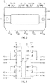
FIG. 2] FIG. 2 is a view of an appearance of thesemiconductor device 1 according to an embodiment of the present invention. - [
FIG. 3] FIG. 3 is a circuit diagram of thesemiconductor device 1 according to an embodiment of the present invention. - [
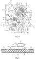
FIG. 4] FIG. 4 is an expanded plan view ofFIG. 1 . - [
FIG. 5] FIG. 5 is a cross-sectional view taken along the A-A line inFIG. 4 . - Hereafter, a semiconductor device according to an embodiment of the present invention is described with reference to the drawings. Notably, constituents having the equivalent functions are given the same signs in the drawings.
- First, a circuit configuration of a
semiconductor device 1 according to an embodiment of the present invention is described with reference toFIG. 3 . As shown inFIG. 3 , thesemiconductor device 1 has a first half bridge circuit and a second half bridge circuit. The first half bridge circuit includes a high-side switching part constituted of a GaN-HEMT 10 and a MOS-FET 15 which are in cascade connection, and a low-side switching part constituted of a GaN-HEMT 20 and a MOS-FET 25 which are in cascade connection. The second half bridge circuit includes a high-side switching part constituted of a GaN-HEMT 30 and a MOS-FET 35 which are in cascade connection, and a low-side switching part constituted of a GaN-HEMT 40 and a MOS-FET 45 which are in cascade connection. Thesemiconductor device 1 functions, for example, as a DC/DC converter, a rectifier or an inverter. - As shown in
FIG. 3 , abypass capacitor 80 is provided between a terminal T1 and a terminal T7, and abypass capacitor 90 is provided between a terminal T11 and the terminal T7. Thebypass capacitor 80 is provided between the drain electrode of the GaN-HEMT 10 and the source electrode of the MOS-FET 25. Thebypass capacitor 90 is provided between the drain electrode of the GaN-HEMT 30 and the source electrode of the MOS-FET 45. Providing thebypass capacitors bypass capacitors semiconductor device 1 and for removing various kinds of noise. - Notably, the capacitances of the
bypass capacitors HEMTs - Next, a specific configuration of the
semiconductor device 1 is described with reference toFIG. 1 andFIG. 2 . - The
semiconductor device 1 includes an insulatingsubstrate 2, the GaN-HEMTs FETs bypass capacitors part 95. As shown inFIG. 1 , thesemiconductor device 1 is configured to be in bilateral symmetry. A first half bridge circuit is formed on one side, and a second half bridge circuit is formed on the other side. - Moreover, the
semiconductor device 1 further includesconductive pattern parts conductive pattern parts substrate 2. Theconductive pattern parts 51 to 59 and 61 to 64 are formed, for example, by patterning the insulatingsubstrate 2 with a copper foil. Detailed description of the individual conductive pattern parts is made later. - The insulating
substrate 2 is composed of an insulating material, and, for example, composed of a material such as ceramics that is excellent in heat dissipation. As shown inFIG. 1 , the insulatingsubstrate 2 has asubstrate side 2a (first substrate side) and asubstrate side 2b (second substrate side) opposite to thesubstrate side 2a. The substrate sides 2a and 2b are sides from which various terminals of thesemiconductor device 1 protrude in plan view. Namely, terminals T1, T4, T7, T11 and T14 protrude from thesubstrate side 2a in plan view, and terminals T2, T3, T5, T6, T12, T13, T15 and T16 protrude from thesubstrate side 2b in plan view. Notably, on the back surface of the insulatingsubstrate 2, aconductive pattern part 65 connected to a radiator (not shown) such as a heat sink is formed so as to cover the back surface (seeFIG. 5 ). - The GaN-
HEMTs HEMTs - The MOS-
FETs FETs - As shown in
FIG. 1 , thebypass capacitor 80 has anelectrode 81 and anelectrode 82. Thebypass capacitor 90 has anelectrode 91 and anelectrode 92. Thebypass capacitors part 95 along with the electronic components such as the GaN-HEMTs FETs - The
semiconductor device 1 further includes the terminals T1, T2, T3, T4, T5, T6, T7, T11, T12, T13, T14, T15 and T16 for connection to external devices (IC chips such as a driver, and a power supply). These terminals are provided so as to come and protrude from the planes ofFIG. 1 andFIG. 2 . Inner leads of these terminals and portions other than the back surface of the insulatingsubstrate 2 are resin-sealed with the resin-sealedpart 95. Notably, as shown inFIG. 2 , through holes H1 and H2 for inserting attachment screws therethrough are provided in thesemiconductor device 1. - Here, details of the individual terminals of the
semiconductor device 1 are described. - The terminals T1 and T11 are terminals connected to the high voltage side of a power supply (not shown) (high voltage-side terminals). Meanwhile, the terminal T7 is a terminal connected to the low voltage side (ground) of the power supply (low voltage-side terminal). Notably, when the power supply circuit of the
semiconductor devices 1 functions as a rectifier, the terminal T1 and the terminal T11 are connected to a load on the output side. - The terminals T2 and T12 are terminals for inputting gate signals to high-side switches of the half bridge circuits therethrough. The terminal T2 is electrically connected to a
gate electrode 18 of the MOS-FET 15, and the terminal T12 is electrically connected to agate electrode 38 of the MOS-FET 35. The terminals T5 and T15 are terminals for inputting gate signals to low-side switches of the half bridge circuits therethrough. The terminal T5 is electrically connected to agate electrode 28 of the MOS-FET 25, and the terminal T15 is electrically connected to agate electrode 48 of the MOS-FET 45. These terminals T2, T5, T12 and T15 are electrically connected to a driver (not shown) driving the power supply circuit. - The terminal T3 is a terminal for monitoring a voltage between the MOS-
FET 15 and the GaN-HEMT 20. Likewise, the terminal T13 is a terminal for monitoring a voltage between the MOS-FET 35 and the GaN-HEMT 40. The terminal T4 is a terminal for outputting an output voltage of the first half bridge circuit therethrough. Likewise, the terminal T14 is a terminal for outputting an output voltage of the second half bridge circuit. Notably, when the power supply circuit of thesemiconductor device 1 functions as a rectifier, an AC power supply on the input side is connected between the terminal T4 and the terminal T14. - The terminal T6 is a terminal for monitoring a voltage between the MOS-
FET 25 and the terminal T7. Likewise, the terminal T16 is a terminal for monitoring a voltage between the MOS-FET 45 and the terminal T7. - Next, the GaN-
HEMTs FETs - The GaN-
HEMTs FIG. 4 and FIG. 5 , the GaN-HEMT 20 has a drain electrode 21 (third GaN main electrode), a source electrode 22 (fourth GaN main electrode) and a gate electrode 23 (second GaN gate electrode). Likewise, the GaN-HEMT 10 has a drain electrode 11 (first GaN main electrode), a source electrode (second GaN main electrode; not shown) and a gate electrode 13 (first GaN gate electrode). The GaN-HEMT 30 has a drain electrode 31 (fifth GaN main electrode), a source electrode (sixth GaN main electrode; not shown) and a gate electrode 33 (third GaN gate electrode). The GaN-HEMT 40 has a drain electrode 41 (seventh GaN main electrode), a source electrode (eighth GaN main electrode; not shown) and a gate electrode 43 (fourth GaN gate electrode). - Notably, the GaN-
HEMTs HEMT 10, the drain electrode provided on the back surface of the GaN-HEMT 10 is connected to theconductive pattern part 51 via solder. Theconductive pattern part 51 and theconductive pattern part 53 are joined together to be configured as an integrated conductive pattern part. Likewise also in the case of the GaN-HEMT 20, the drain electrode provided on the back surface of the GaN-HEMT 20 is connected to theconductive pattern part 52, and theconductive pattern part 52 and theconductive pattern part 55 are joined together. - The MOS-
FETs FIG. 4 and FIG. 5 , the MOS-FET 25 has a drain electrode 26 (third MOS main electrode), a source electrode 27 (fourth MOS main electrode) and the gate electrode 28 (second MOS gate electrode). Likewise, the MOS-FET 15 has a drain electrode (first MOS main electrode; not shown), a source electrode 17 (second MOS main electrode) and the gate electrode 18 (first MOS gate electrode). The MOS-FET 35 includes a drain electrode (fifth MOS main electrode; not shown), a source electrode 37 (sixth MOS main electrode) and the gate electrode 38 (third MOS gate electrode). The MOS-FET 45 includes a drain electrode (seventh MOS main electrode; not shown), a source electrode 47 (eighth MOS main electrode) and the gate electrode 48 (fourth MOS gate electrode). - As shown in
FIG. 5 , the MOS-FET 25 is disposed on the GaN-HEMT 20 such that thedrain electrode 26 of the MOS-FET 25 is electrically connected to thesource electrode 22 of the GaN-HEMT 20. Similarly to the MOS-FET 25, the MOS-FETs HEMTs FET 15 is electrically connected to the source electrode of the GaN-HEMT 10 via solder. The drain electrode of the MOS-FET 35 is electrically connected to the source electrode of the GaN-HEMT 30 via solder. The drain electrode of the MOS-FET 45 is electrically connected to the source electrode of the GaN-HEMT 40 via solder. - The
drain electrode 11 of the GaN-HEMT 10 is electrically connected to theconductive pattern part 53 via ametal wire 3. Further, thedrain electrode 11 is electrically connected to the high voltage-side terminal (terminal T1) via theconductive pattern part 53. The source electrode (not shown) of the GaN-HEMT 10 is connected to the drain electrode of the MOS-FET 15 via solder. Thegate electrode 13 of the GaN-HEMT 10 is electrically connected to theconductive pattern part 54 via ametal wire 5. Further, thisgate electrode 13 is electrically connected to thesource electrode 17 of the MOS-FET 15 via theconductive pattern part 54. - The
drain electrode 21 of the GaN-HEMT 20 is electrically connected to theconductive pattern part 54 via ametal wire 3. The source electrode of the GaN-HEMT 20 is connected to the drain electrode of the MOS-FET 25 via solder. Thegate electrode 23 of the GaN-HEMT 20 is electrically connected to theconductive pattern part 55 via ametal wire 6. Further, thisgate electrode 23 is electrically connected to thesource electrode 27 of the MOS-FET 25 via theconductive pattern part 55. - The
drain electrode 31 of the GaN-HEMT 30 is electrically connected to theconductive pattern part 58 via ametal wire 3. The source electrode of the GaN-HEMT 20 is connected to the drain electrode of the MOS-FET 35 via solder. Thegate electrode 33 of the GaN-HEMT 30 is electrically connected to theconductive pattern part 59 via a metal wire 7. Further, thegate electrode 33 is electrically connected to thesource electrode 37 of the MOS-FET 35 via theconductive pattern part 59. - The
drain electrode 41 of the GaN-HEMT 40 is electrically connected to theconductive pattern part 59 via ametal wire 3. The source electrode of the GaN-HEMT 40 is connected to the drain electrode of the MOS-FET 45 via solder. Thegate electrode 43 of the GaN-HEMT 40 is electrically connected to theconductive pattern part 55 via ametal wire 8. Further, thegate electrode 43 is electrically connected to thesource electrode 47 of the MOS-FET 45 via theconductive pattern part 55. - The source electrode 17 of the MOS-
FET 15 is electrically connected to theconductive pattern part 54 via ametal wire 3. Thegate electrode 18 of the MOS-FET 15 is electrically connected to theconductive pattern part 61 via ametal wire 3. - The source electrode 27 of the MOS-
FET 25 is electrically connected to theconductive pattern part 55 via ametal wire 3. This source electrode 27 is electrically connected to the low voltage-side terminal (terminal T7) via theconductive pattern part 55. Thegate electrode 28 of the MOS-FET 25 is electrically connected to theconductive pattern part 62 via ametal wire 3. - The source electrode 37 of the MOS-
FET 35 is electrically connected to theconductive pattern part 59 via ametal wire 3. Thegate electrode 38 of the MOS-FET 35 is electrically connected to theconductive pattern part 63 via ametal wire 3. - The source electrode 47 of the MOS-
FET 45 is electrically connected to theconductive pattern part 55 via ametal wire 3. Thegate electrode 48 of the MOS-FET 45 is electrically connected to theconductive pattern part 64 via ametal wire 3. - Notably, while the
metal wires 3 are aluminum wires (Al wires), they may be composed of another metal material. While themetal wires metal wires gate electrodes - Notably, for electrically connecting the semiconductor switching parts and the conductive pattern parts together, in place of the metal wires, connectors composed of conductive plate materials may be used.
- Next, referring to
FIG. 1 , the individual conductive pattern parts of thesemiconductor device 1 are described in detail. - The
conductive pattern parts conductive pattern parts conductive pattern part 55 is shared by the first half bridge circuit and the second half bridge circuit. Moreover, as shown inFIG. 1 , theconductive pattern part 55 is formed to have a shape in bilateral symmetry. - The
conductive pattern part 51 is a conductive pattern part for implementing the GaN-HEMT 10. Likewise, theconductive pattern part 52 is a conductive pattern part for implementing the GaN-HEMT 20. Theconductive pattern part 56 is a conductive pattern part for implementing the GaN-HEMT 30. Theconductive pattern part 57 is a conductive pattern part for implementing the GaN-HEMT 40. - In the present embodiment, as shown in
FIG. 1 , theconductive pattern parts HEMTs HEMT 10 is disposed on theconductive pattern part 51. The GaN-HEMT 20 is disposed on theconductive pattern part 52. The GaN-HEMT 30 is disposed on theconductive pattern part 56. The GaN-HEMT 40 is disposed on theconductive pattern part 57. - To the
conductive pattern part 53, thedrain electrode 11 of the GaN-HEMT 10 is electrically connected via themetal wire 3, and the terminal T1 and theelectrode 81 of thebypass capacitor 80 are connected via solder. Likewise, to theconductive pattern part 58, thedrain electrode 31 of the GaN-HEMT 30 is electrically connected via themetal wire 3, and the terminal T11 and theelectrode 91 of thebypass capacitor 90 are connected via solder. - The
conductive pattern part 54 electrically connects the high-side switch (the GaN-HEMT 10 and the MOS-FET 15) and the low-side switch (the GaN-HEMT 20 and the MOS-FET 25) of the first half bridge circuit together. Moreover, to theconductive pattern part 54, the terminals T3 and T4 are electrically connected via solder. Moreover, to theconductive pattern part 54, one end of themetal wire 5 whose other end is connected to thegate electrode 13 of the GaN-HEMT 10 is connected. - Likewise, the
conductive pattern part 59 electrically connects the high-side switch (the GaN-HEMT 30 and the MOS-FET 35) and the low-side switch (the GaN-HEMT 40 and the MOS-FET 45) of the second half bridge circuit together. Moreover, to theconductive pattern part 59, the terminal T13 and the terminal T14 are electrically connected via solder. Moreover, to theconductive pattern part 59, one end of the metal wire 7 whose other end is connected to thegate electrode 33 of the GaN-HEMT 30 is connected. - The
electrode 82 of thebypass capacitor 80 is electrically connected to theconductive pattern part 55 via solder, and thesource electrode 27 of the MOS-FET 25 is electrically connected thereto via themetal wire 3. Furthermore, theelectrode 92 of thebypass capacitor 90 is electrically connected to theconductive pattern part 55 via solder, and thesource electrode 47 of the MOS-FET 45 is electrically connected thereto via themetal wire 3. Moreover, the terminals T6, T7 and T16 are electrically connected to theconductive pattern part 55 via solder. - As shown in
FIG. 1 , to theconductive pattern part 55, thegate electrode 23 of the GaN-HEMT 20 is electrically connected via themetal wire 6, and thegate electrode 43 of the GaN-HEMT 40 is electrically connected via themetal wire 8. - The
conductive pattern part 61 is a conductive pattern part for electrically connecting thegate electrode 18 of the MOS-FET 15 and the terminal T2 together. To thisconductive pattern part 61, thegate electrode 18 is electrically connected via themetal wire 3, and the terminal T2 is electrically connected via solder. Likewise, theconductive pattern part 63 is a conductive pattern part for electrically connecting thegate electrode 38 of the MOS-FET 35 and the terminal T12 together. To thisconductive pattern part 63, thegate electrode 38 is electrically connected via themetal wire 3, and the terminal T12 is electrically connected via solder. - The
conductive pattern part 62 is a conductive pattern part for electrically connecting thegate electrode 28 of the MOS-FET 25 and the terminal T5 together. To thisconductive pattern part 62, thegate electrode 28 is electrically connected via themetal wire 3, and the terminal T5 is electrically connected via solder. Likewise, theconductive pattern part 64 is a conductive pattern part for electrically connecting thegate electrode 48 of the MOS-FET 45 and the terminal T15 together. To thisconductive pattern part 64, thegate electrode 48 is electrically connected via themetal wire 3, and the terminal T15 is electrically connected via solder. - Next, arrangement relation between the GaN-
HEMT 10 and the GaN-HEMT 20 is described. - As shown in
FIG. 4 , the GaN-HEMT 10 and the GaN-HEMT 20 are substantially quadrangular in plan view. The GaN-HEMT 10 has a side S1 (first side) and a side S2 (second side) opposite to this side S1. In the present embodiment, the side S1 and the side S2 are substantially parallel to each other. Likewise, the GaN-HEMT 20 has a side S3 (third side) and a side S4 (fourth side) opposite to this side S3. In the present embodiment, the side S3 and the side S4 are substantially parallel to each other. - The
drain electrode 11 of the GaN-HEMT 10 is provided along the side S1. Moreover, thesource electrode 17 of the MOS-FET 15 is provided along the side S2. Thedrain electrode 21 of the GaN-HEMT 20 is provided along the side S3. Moreover, thesource electrode 27 of the MOS-FET 25 is provided along the side S4. - As shown in
FIG. 4 , in thesemiconductor device 1, an imaginary line L1 extending along the side S1 and an imaginary line L2 extending along the side S3 intersect each other. In other words, the imaginary line L1 and the imaginary line L2 are not parallel to each other. Thereby, as compared with the case where the GaN-HEMT 10 and the GaN-HEMT 20 are in parallel arrangement (that is, the case where the imaginary line L1 and the imaginary line L2 are parallel to each other), the bypass capacitor path P1 can be made short, and a parasitic inductance in the bypass capacitor path P1 can be reduced. - Notably, as an angle θ at which the imaginary line L1 and the imaginary line L2 intersect each other is larger, the length of the bypass capacitor path P1 is shorter, which suppresses the parasitic inductance more. However, this meanwhile causes the length of a path between the
source electrode 17 of the MOS-FET 15 and thedrain electrode 21 of the GaN-HEMT 20 to be longer, and a parasitic inductance in this path becomes larger, which leads to the cause of a malfunction of the power supply circuit. With such circumstances taken into consideration, the angle θ at which the imaginary line L1 and the imaginary line L2 intersect each other is preferably not less than 30° and not more than 135°, still preferably not less than 30° and nor more than 60°. In the present embodiment, the angle θ is substantially 45°. - As shown in
FIG. 1 , in the present embodiment, the high-side switch-side GaN-HEMT 10 is disposed such that the imaginary line L1 is substantially parallel to thesubstrate side 2a of the insulatingsubstrate 2. The low-side switch-side GaN-HEMT 20 is disposed such that the imaginary line L2 is oblique to thesubstrate side 2a of the insulatingsubstrate 2. Thereby, a space in an upper center region of the insulatingsubstrate 2 can be easily secured. Namely, a region where themetal wires 3 connected to thesource electrode 27 of the MOS-FET 25 are connected to theconductive pattern part 55, out of theconductive pattern part 55, can be made wide. As a result, the parasitic inductance in the bypass capacitor path P1 can be reduced. - Notably, as shown in
FIG. 1 , in the present embodiment, thesemiconductor device 1 has a configuration in bilateral symmetry. Namely, the GaN-HEMT 10 and the GaN-HEMT 30 are symmetrically disposed with theconductive pattern part 55 interposed therebetween. The GaN-HEMT 20 and the GaN-HEMT 40 are symmetrically disposed with theconductive pattern part 55 interposed therebetween. Thebypass capacitor 80 and thebypass capacitor 90 are also symmetrically disposed with theconductive pattern part 55 interposed therebetween. Further, theconductive pattern part 55 is shared by the two half bridge circuits. Such a configuration of thesemiconductor device 1 in bilateral symmetry as above enables theconductive pattern part 55 to be wide, and parasitic inductances in the bypass capacitor paths P1 and P2 to be further reduced. - As shown in
FIG. 4 , the GaN-HEMT 20 has a side S5 (fifth side) connecting the side S3 and the side S4. Theconductive pattern part 55 has aconductive pattern side 55S opposite to the side S5. - As shown in
FIG. 4 , thegate electrode 23 of the GaN-HEMT 20 is electrically connected to theconductive pattern part 55 via themetal wire 6. Themetal wire 6 is perpendicular to the side S5 of the GaN-HEMT 20 and theconductive pattern side 55S of theconductive pattern part 55. Thereby, thegate electrode 23 is connected to theconductive pattern part 55 at the shortest distance, and themetal wire 6 can be made short. Notably, in the present application, the term "perpendicular" includes not only the case of intersection strictly at 90° but also the case of being substantially perpendicular for the purpose of allowing a tolerance and an error in production. - In the present embodiment, similarly to the
metal wire 6, themetal wire 8 electrically connecting thegate electrode 43 of the GaN-HEMT 40 and theconductive pattern part 55 together is also configured so as to have the shortest length. - Notably, the same holds true for the case of using connectors in place of the
metal wires metal wire 6, thegate electrode 23 of the GaN-HEMT 20 is electrically connected to theconductive pattern part 55 via the connector. This connector is perpendicular to the side S5 of the GaN-HEMT 20 and theconductive pattern side 55S of theconductive pattern part 55. Accordingly, generally speaking, a connection member such as a metal wire and a connector is provided so as to be perpendicular to the side S5 of the GaN-HEMT 20 and theconductive pattern side 55S of theconductive pattern part 55. - As described above, in the
semiconductor device 1 of the present embodiment, the GaN-HEMT 10 and the GaN-HEMT 20 are disposed on the insulatingsubstrate 2 such that the imaginary line L1 and the imaginary line L2 intersect each other. Thereby, the bypass capacitor path P1 can be made short, and the parasitic inductance in the bypass capacitor path P1 can be reduced. Furthermore, in thesemiconductor device 1, themetal wire 6 electrically connecting thegate electrode 23 of the GaN-HEMT 20 and theconductive pattern part 55 together is substantially perpendicular to the side S5 of the GaN-HEMT 20 and theconductive pattern side 55S of theconductive pattern part 55. Thereby, thegate electrode 23 of the GaN-HEMT 20 is connected to theconductive pattern part 55 at the shortest distance by themetal wire 6. Making themetal wire 6 short as above can suppress the parasitic inductance in themetal wire 6. In the present embodiment, making both the length of the bypass capacitor path P1 and the length of themetal wire 6 short can suppress a malfunction of the GaN-HEMT 20. Therefore, according to the present embodiment, a malfunction of a power supply circuit having GaN-HEMTs can be suppressed. - As above, the semiconductor device according to the present embodiment has been described. Notably, not limited to the aforementioned half bridge circuit, the semiconductor device according to the present invention can also be applied to power supply circuits with other configurations, such as a full bridge circuit and a push-pull circuit, as long as each has semiconductor switching elements in cascade connection.
- Notably, similarly also as to the GaN-
HEMT 10, themetal wire 5 may be provided so as to have the shortest length, thismetal wire 5 electrically connecting thegate electrode 13 to theconductive pattern part 54. Namely, as shown inFIG. 4 , themetal wire 5 may be provided so as to be perpendicular to a side S6 connecting the side S1 and the side S2 and aconductive pattern side 54S opposite to the side S6. Thereby, a malfunction of the power supply circuit can be further suppressed. - Based on the aforementioned description, while those skilled in the art may conceive of additional effects and various alterations of the present invention, aspects of the present invention are not limited to the aforementioned individual embodiments. Components across different embodiments may be properly combined. Various additions, modifications and partial deletions may occur without departing from the conceptual ideas and spirit of the present invention derived from the contents and their equivalents as defined in the appended claims.
-
- 1 Semiconductor device
- 2 Insulating substrate
- 2a, 2b Substrate side
- 3, 5, 6, 7, 8 Metal wire
- 10, 20, 30, 40 GaN-HEMT
- 11, 21, 31, 41 Drain electrode
- 22 Source electrode
- 13, 23, 33, 43 Gate electrode
- 15, 25, 35, 45 MOS-FET
- 26 Drain electrode
- 17, 27, 37, 47 Source electrode
- 18, 28, 38, 48 Gate electrode
- 51, 52, 53, 54, 55, 56, 57, 58, 59, 61, 62, 63, 64, 65 Conductive pattern part
- 54S, 55S Conductive pattern side
- 80, 90 Bypass capacitor
- 81, 82, 91, 92 Electrode
- 95 Resin-sealed part
- H1, H2 Through hole
- L1, L2 Imaginary line
- N1, N2, N3, N4 Node
- S1, S2, S3, S4, S5, S6 Side
- T1, T2, T3, T4, T5, T6, T7, T11, T12, T13, T14, T15, T16 Terminal
Claims (12)
- A semiconductor device comprising:an insulating substrate;a first conductive pattern part formed on the insulating substrate;a second conductive pattern part formed on the insulating substrate;a third conductive pattern part formed on the insulating substrate;a fourth conductive pattern part formed on the insulating substrate;a fifth conductive pattern part formed on the insulating substrate;a first GaN-HEMT having a first GaN main electrode, a second GaN main electrode and a first GaN gate electrode and disposed on the first conductive pattern part;a first MOS-FET having a first MOS main electrode, a second MOS main electrode and a first MOS gate electrode, the first MOS main electrode being electrically connected to the second GaN main electrode;a second GaN-HEMT having a third GaN main electrode, a fourth GaN main electrode and a second GaN gate electrode and disposed on the second conductive pattern part;a second MOS-FET having a third MOS main electrode, a fourth MOS main electrode and a second MOS gate electrode, the third MOS main electrode being electrically connected to the fourth GaN main electrode; anda bypass capacitor having a first electrode and a second electrode,the first GaN main electrode of the first GaN-HEMT being electrically connected to the third conductive pattern part, the second MOS main electrode of the first MOS-FET being electrically connected to the fourth conductive pattern part, the third GaN main electrode of the second GaN-HEMT being electrically connected to the fourth conductive pattern part, the fourth MOS main electrode of the second MOS-FET being electrically connected to the fifth conductive pattern part, the first electrode of the bypass capacitor being electrically connected to the third conductive pattern part, the second electrode of the bypass capacitor being electrically connected to the fifth conductive pattern part,the first GaN-HEMT having a first side and a second side opposite to the first side, the second GaN-HEMT having a third side and a fourth side opposite to the third side,the first GaN main electrode of the first GaN-HEMT being provided along the first side, the third GaN main electrode of the second GaN-HEMT being provided along the third side, a first imaginary line extending along the first side and a second imaginary line extending along the third side intersecting each other,the second GaN-HEMT having a fifth side connecting the third side and the fourth side, the fifth conductive pattern part having a conductive pattern side opposite to the fifth side,the second GaN gate electrode of the second GaN-HEMT being electrically connected to the fifth conductive pattern part via a connection member, the connection member being perpendicular to the fifth side and the conductive pattern side.
- The semiconductor device according to claim 1, wherein the first GaN-HEMT and the second GaN-HEMT are normally-on transistors, and the first MOS-FET and the second MOS-FET are normally-off transistors.
- The semiconductor device according to claim 1, wherein the connection member is a metal wire or a connector.
- The semiconductor device according to claim 1, wherein the first GaN main electrode of the first GaN-HEMT is electrically connected to a high voltage-side terminal via the third conductive pattern part, and the fourth MOS main electrode of the second MOS-FET is electrically connected to a low voltage-side terminal via the fifth conductive pattern part.
- The semiconductor device according to claim 4, wherein
the insulating substrate has a first substrate side from which the high voltage-side terminal and the low voltage-side terminal protrude in plan view, and a second substrate side opposite to the first substrate side, and
the first GaN-HEMT is disposed such that the first imaginary line is parallel to the first substrate side, and the second GaN-HEMT is disposed such that the second imaginary line is oblique to the first substrate side. - The semiconductor device according to claim 1, wherein an angle at which the first imaginary line and the second imaginary line intersect each other is not less than 30° and not more than 60°.
- The semiconductor device according to claim 1, wherein an angle at which the first imaginary line and the second imaginary line intersect each other is 45°.
- The semiconductor device according to claim 1, wherein
the first GaN-HEMT has a sixth side connecting the first side and the second side, and the fourth conductive pattern part has a conductive pattern side opposite to the sixth side, and
the first GaN gate electrode of the first GaN-HEMT is electrically connected to the fourth conductive pattern part via a connection member, and the connection member is perpendicular to the sixth side and the conductive pattern side. - The semiconductor device according to claim 1, wherein the first MOS-FET is disposed on the first GaN-HEMT, and the second MOS-FET is disposed on the second GaN-HEMT.
- The semiconductor device according to claim 1, wherein the bypass capacitor is resin-sealed along with the first GaN-HEMT, the second GaN-HEMT, the first MOS-FET and the second MOS-FET.
- The semiconductor device according to claim 1, further comprising:a sixth conductive pattern part formed on the insulating substrate;a seventh conductive pattern part formed on the insulating substrate;an eighth conductive pattern part formed on the insulating substrate;a ninth conductive pattern part formed on the insulating substrate;a third GaN-HEMT having a fifth GaN main electrode, a sixth GaN main electrode and a third GaN gate electrode and disposed on the sixth conductive pattern part;a third MOS-FET having a fifth MOS main electrode, a sixth MOS main electrode and a third MOS gate electrode, the fifth MOS main electrode electrically connected to the sixth GaN main electrode;a fourth GaN-HEMT having a seventh GaN main electrode, an eighth GaN main electrode and a fourth GaN gate electrode and disposed on the seventh conductive pattern part; anda fourth MOS-FET having a seventh MOS main electrode, an eighth MOS main electrode and a fourth MOS gate electrode, the seventh MOS main electrode electrically connected to the eighth GaN main electrode, whereinthe fifth GaN main electrode of the third GaN-HEMT is electrically connected to the eighth conductive pattern part, the sixth MOS main electrode of the third MOS-FET is electrically connected to the ninth conductive pattern part, the seventh GaN main electrode of the fourth GaN-HEMT is electrically connected to the ninth conductive pattern part, and the eighth MOS main electrode of the fourth MOS-FET is electrically connected to the fifth conductive pattern part, andthe first GaN-HEMT and the third GaN-HEMT are symmetrically disposed with the fifth conductive pattern part interposed therebetween, and the second GaN-HEMT and the fourth GaN-HEMT are symmetrically disposed with the fifth conductive pattern part interposed therebetween.
- The semiconductor device according to claim 11, further comprising
another bypass capacitor having a third electrode and a fourth electrode, wherein
the third electrode is electrically connected to the eighth conductive pattern part, and the fourth electrode is electrically connected to the fifth conductive pattern part, and
the bypass capacitor and the other bypass capacitor are symmetrically disposed with the fifth conductive pattern part interposed therebetween.
Applications Claiming Priority (1)
| Application Number | Priority Date | Filing Date | Title |
|---|---|---|---|
| PCT/JP2017/022567 WO2018235137A1 (en) | 2017-06-19 | 2017-06-19 | Semiconductor device |
Publications (3)
| Publication Number | Publication Date |
|---|---|
| EP3644361A1 true EP3644361A1 (en) | 2020-04-29 |
| EP3644361A4 EP3644361A4 (en) | 2020-06-17 |
| EP3644361B1 EP3644361B1 (en) | 2021-08-11 |
Family
ID=62779921
Family Applications (1)
| Application Number | Title | Priority Date | Filing Date |
|---|---|---|---|
| EP17808300.2A Active EP3644361B1 (en) | 2017-06-19 | 2017-06-19 | Semiconductor device |
Country Status (6)
| Country | Link |
|---|---|
| US (1) | US10199486B2 (en) |
| EP (1) | EP3644361B1 (en) |
| JP (1) | JP6352556B1 (en) |
| KR (1) | KR102009590B1 (en) |
| CN (1) | CN109429529B (en) |
| WO (1) | WO2018235137A1 (en) |
Families Citing this family (4)
| Publication number | Priority date | Publication date | Assignee | Title |
|---|---|---|---|---|
| US12567607B2 (en) | 2019-04-26 | 2026-03-03 | The Noco Company | Lithium-ion battery management system (BMS) having compact heat sinking arrangement, lithium-ion battery having BMS with compact heat sinking arrangement, and method of making BMS with compact heat sinking arrangement |
| USD937793S1 (en) * | 2019-04-26 | 2021-12-07 | The Noco Company | Circuit board |
| US11069640B2 (en) * | 2019-06-14 | 2021-07-20 | Cree Fayetteville, Inc. | Package for power electronics |
| JP7361112B2 (en) * | 2019-06-24 | 2023-10-13 | ローム株式会社 | semiconductor equipment |
Family Cites Families (19)
| Publication number | Priority date | Publication date | Assignee | Title |
|---|---|---|---|---|
| JPS62150871A (en) | 1985-12-25 | 1987-07-04 | Hitachi Ltd | Semiconductor device |
| JP4009056B2 (en) | 2000-05-25 | 2007-11-14 | 三菱電機株式会社 | Power module |
| JP4066644B2 (en) * | 2001-11-26 | 2008-03-26 | 株式会社豊田自動織機 | Semiconductor device and wiring method of semiconductor device |
| JP4426955B2 (en) * | 2004-11-30 | 2010-03-03 | 株式会社ルネサステクノロジ | Semiconductor device |
| JP5333814B2 (en) | 2007-09-12 | 2013-11-06 | アイシン精機株式会社 | Power semiconductor module, inverter device, and inverter-integrated motor |
| JP5353815B2 (en) * | 2010-05-19 | 2013-11-27 | 三菱電機株式会社 | Semiconductor module |
| WO2013046439A1 (en) * | 2011-09-30 | 2013-04-04 | ルネサスエレクトロニクス株式会社 | Semiconductor device |
| WO2013046824A1 (en) | 2011-09-30 | 2013-04-04 | ローム株式会社 | Semiconductor device |
| JP2013153027A (en) * | 2012-01-24 | 2013-08-08 | Fujitsu Ltd | Semiconductor device and power supply device |
| DE102012202765B3 (en) * | 2012-02-23 | 2013-04-18 | Semikron Elektronik Gmbh & Co. Kg | Semiconductor module |
| US9269789B2 (en) * | 2013-03-15 | 2016-02-23 | Semiconductor Components Industries, Llc | Method of forming a high electron mobility semiconductor device and structure therefor |
| JP2015029040A (en) | 2013-07-05 | 2015-02-12 | サンケン電気株式会社 | Semiconductor module, LED driving device, and LED lighting device |
| WO2015040727A1 (en) * | 2013-09-20 | 2015-03-26 | 株式会社日立製作所 | Semiconductor integrated circuit device |
| JP6333693B2 (en) * | 2014-09-30 | 2018-05-30 | ルネサスエレクトロニクス株式会社 | Semiconductor device |
| US20160293597A1 (en) * | 2015-04-06 | 2016-10-06 | Infineon Technologies Austria Ag | Integrated Semiconductor Device |
| US9793793B2 (en) * | 2015-06-26 | 2017-10-17 | Sharp Kabushiki Kaisha | Power factor correction circuit and power supply device |
| WO2017002390A1 (en) * | 2015-06-30 | 2017-01-05 | シャープ株式会社 | Circuit module |
| CN105932016A (en) * | 2016-06-12 | 2016-09-07 | 重庆大学 | Dynamic and static current-sharing and multi-chip paralleled power module |
| CN105914185B (en) * | 2016-06-21 | 2018-07-31 | 华中科技大学 | A kind of encapsulating structure and packaging method of silicon carbide power device |
-
2017
- 2017-06-19 JP JP2017554108A patent/JP6352556B1/en active Active
- 2017-06-19 WO PCT/JP2017/022567 patent/WO2018235137A1/en not_active Ceased
- 2017-06-19 EP EP17808300.2A patent/EP3644361B1/en active Active
- 2017-06-19 CN CN201780002328.9A patent/CN109429529B/en active Active
- 2017-06-19 KR KR1020177037207A patent/KR102009590B1/en active Active
- 2017-06-19 US US15/738,437 patent/US10199486B2/en active Active
Also Published As
| Publication number | Publication date |
|---|---|
| EP3644361B1 (en) | 2021-08-11 |
| KR102009590B1 (en) | 2019-08-09 |
| KR20190087686A (en) | 2019-07-25 |
| CN109429529A (en) | 2019-03-05 |
| JPWO2018235137A1 (en) | 2019-06-27 |
| US10199486B2 (en) | 2019-02-05 |
| WO2018235137A1 (en) | 2018-12-27 |
| EP3644361A4 (en) | 2020-06-17 |
| JP6352556B1 (en) | 2018-07-04 |
| US20180366567A1 (en) | 2018-12-20 |
| CN109429529B (en) | 2022-06-21 |
Similar Documents
| Publication | Publication Date | Title |
|---|---|---|
| US10243477B2 (en) | Semiconductor device having a bypass capacitor | |
| JP6909881B2 (en) | Switching circuit with ferrite beads | |
| US20130015495A1 (en) | Stacked Half-Bridge Power Module | |
| WO2014185050A1 (en) | Semiconductor device | |
| US11626790B2 (en) | Power conversion device minimizing footprint | |
| EP3644361B1 (en) | Semiconductor device | |
| JP6168145B2 (en) | Semiconductor device | |
| US9824976B1 (en) | Single-sided power device package | |
| US20220320054A1 (en) | Semiconductor device | |
| CN111279476B (en) | Semiconductor device | |
| US10218257B2 (en) | Power converter having parallel-connected semiconductor switches | |
| US20230307332A1 (en) | Power Semiconductor Module and Method for Producing a Power Semiconductor Module | |
| US20200403512A1 (en) | Control circuit module, electronic component connection structure, and power conversion device | |
| US20250364505A1 (en) | Semiconductor device | |
| US12588570B2 (en) | Semiconductor device | |
| US20250364506A1 (en) | Semiconductor device |
Legal Events
| Date | Code | Title | Description |
|---|---|---|---|
| STAA | Information on the status of an ep patent application or granted ep patent |
Free format text: STATUS: UNKNOWN |
|
| STAA | Information on the status of an ep patent application or granted ep patent |
Free format text: STATUS: THE INTERNATIONAL PUBLICATION HAS BEEN MADE |
|
| PUAI | Public reference made under article 153(3) epc to a published international application that has entered the european phase |
Free format text: ORIGINAL CODE: 0009012 |
|
| STAA | Information on the status of an ep patent application or granted ep patent |
Free format text: STATUS: REQUEST FOR EXAMINATION WAS MADE |
|
| 17P | Request for examination filed |
Effective date: 20171213 |
|
| AK | Designated contracting states |
Kind code of ref document: A1 Designated state(s): AL AT BE BG CH CY CZ DE DK EE ES FI FR GB GR HR HU IE IS IT LI LT LU LV MC MK MT NL NO PL PT RO RS SE SI SK SM TR |
|
| AX | Request for extension of the european patent |
Extension state: BA ME |
|
| A4 | Supplementary search report drawn up and despatched |
Effective date: 20200518 |
|
| RIC1 | Information provided on ipc code assigned before grant |
Ipc: H01L 25/07 20060101AFI20200512BHEP Ipc: H01L 23/373 20060101ALI20200512BHEP Ipc: H01L 25/18 20060101ALI20200512BHEP Ipc: H01L 29/20 20060101ALI20200512BHEP Ipc: H02M 7/00 20060101ALN20200512BHEP Ipc: H01L 25/16 20060101ALN20200512BHEP Ipc: H01L 23/498 20060101ALI20200512BHEP Ipc: H01L 23/538 20060101ALN20200512BHEP |
|
| DAV | Request for validation of the european patent (deleted) | ||
| DAX | Request for extension of the european patent (deleted) | ||
| GRAP | Despatch of communication of intention to grant a patent |
Free format text: ORIGINAL CODE: EPIDOSNIGR1 |
|
| RIC1 | Information provided on ipc code assigned before grant |
Ipc: H01L 25/07 20060101AFI20201216BHEP Ipc: H01L 25/16 20060101ALN20201216BHEP Ipc: H02M 7/00 20060101ALN20201216BHEP Ipc: H01L 23/498 20060101ALI20201216BHEP Ipc: H01L 29/20 20060101ALI20201216BHEP Ipc: H01L 23/373 20060101ALI20201216BHEP Ipc: H01L 23/538 20060101ALN20201216BHEP Ipc: H01L 25/18 20060101ALI20201216BHEP |
|
| STAA | Information on the status of an ep patent application or granted ep patent |
Free format text: STATUS: GRANT OF PATENT IS INTENDED |
|
| INTG | Intention to grant announced |
Effective date: 20210121 |
|
| GRAS | Grant fee paid |
Free format text: ORIGINAL CODE: EPIDOSNIGR3 |
|
| GRAA | (expected) grant |
Free format text: ORIGINAL CODE: 0009210 |
|
| STAA | Information on the status of an ep patent application or granted ep patent |
Free format text: STATUS: THE PATENT HAS BEEN GRANTED |
|
| AK | Designated contracting states |
Kind code of ref document: B1 Designated state(s): AL AT BE BG CH CY CZ DE DK EE ES FI FR GB GR HR HU IE IS IT LI LT LU LV MC MK MT NL NO PL PT RO RS SE SI SK SM TR |
|
| REG | Reference to a national code |
Ref country code: CH Ref legal event code: EP |
|
| REG | Reference to a national code |
Ref country code: DE Ref legal event code: R096 Ref document number: 602017043948 Country of ref document: DE |
|
| REG | Reference to a national code |
Ref country code: IE Ref legal event code: FG4D Ref country code: AT Ref legal event code: REF Ref document number: 1420273 Country of ref document: AT Kind code of ref document: T Effective date: 20210915 |
|
| REG | Reference to a national code |
Ref country code: LT Ref legal event code: MG9D |
|
| REG | Reference to a national code |
Ref country code: NL Ref legal event code: MP Effective date: 20210811 |
|
| REG | Reference to a national code |
Ref country code: AT Ref legal event code: MK05 Ref document number: 1420273 Country of ref document: AT Kind code of ref document: T Effective date: 20210811 |
|
| PG25 | Lapsed in a contracting state [announced via postgrant information from national office to epo] |
Ref country code: LT Free format text: LAPSE BECAUSE OF FAILURE TO SUBMIT A TRANSLATION OF THE DESCRIPTION OR TO PAY THE FEE WITHIN THE PRESCRIBED TIME-LIMIT Effective date: 20210811 Ref country code: AT Free format text: LAPSE BECAUSE OF FAILURE TO SUBMIT A TRANSLATION OF THE DESCRIPTION OR TO PAY THE FEE WITHIN THE PRESCRIBED TIME-LIMIT Effective date: 20210811 Ref country code: BG Free format text: LAPSE BECAUSE OF FAILURE TO SUBMIT A TRANSLATION OF THE DESCRIPTION OR TO PAY THE FEE WITHIN THE PRESCRIBED TIME-LIMIT Effective date: 20211111 Ref country code: NO Free format text: LAPSE BECAUSE OF FAILURE TO SUBMIT A TRANSLATION OF THE DESCRIPTION OR TO PAY THE FEE WITHIN THE PRESCRIBED TIME-LIMIT Effective date: 20211111 Ref country code: PT Free format text: LAPSE BECAUSE OF FAILURE TO SUBMIT A TRANSLATION OF THE DESCRIPTION OR TO PAY THE FEE WITHIN THE PRESCRIBED TIME-LIMIT Effective date: 20211213 Ref country code: RS Free format text: LAPSE BECAUSE OF FAILURE TO SUBMIT A TRANSLATION OF THE DESCRIPTION OR TO PAY THE FEE WITHIN THE PRESCRIBED TIME-LIMIT Effective date: 20210811 Ref country code: SE Free format text: LAPSE BECAUSE OF FAILURE TO SUBMIT A TRANSLATION OF THE DESCRIPTION OR TO PAY THE FEE WITHIN THE PRESCRIBED TIME-LIMIT Effective date: 20210811 Ref country code: FI Free format text: LAPSE BECAUSE OF FAILURE TO SUBMIT A TRANSLATION OF THE DESCRIPTION OR TO PAY THE FEE WITHIN THE PRESCRIBED TIME-LIMIT Effective date: 20210811 Ref country code: ES Free format text: LAPSE BECAUSE OF FAILURE TO SUBMIT A TRANSLATION OF THE DESCRIPTION OR TO PAY THE FEE WITHIN THE PRESCRIBED TIME-LIMIT Effective date: 20210811 Ref country code: HR Free format text: LAPSE BECAUSE OF FAILURE TO SUBMIT A TRANSLATION OF THE DESCRIPTION OR TO PAY THE FEE WITHIN THE PRESCRIBED TIME-LIMIT Effective date: 20210811 |
|
| PG25 | Lapsed in a contracting state [announced via postgrant information from national office to epo] |
Ref country code: PL Free format text: LAPSE BECAUSE OF FAILURE TO SUBMIT A TRANSLATION OF THE DESCRIPTION OR TO PAY THE FEE WITHIN THE PRESCRIBED TIME-LIMIT Effective date: 20210811 Ref country code: LV Free format text: LAPSE BECAUSE OF FAILURE TO SUBMIT A TRANSLATION OF THE DESCRIPTION OR TO PAY THE FEE WITHIN THE PRESCRIBED TIME-LIMIT Effective date: 20210811 Ref country code: GR Free format text: LAPSE BECAUSE OF FAILURE TO SUBMIT A TRANSLATION OF THE DESCRIPTION OR TO PAY THE FEE WITHIN THE PRESCRIBED TIME-LIMIT Effective date: 20211112 |
|
| PG25 | Lapsed in a contracting state [announced via postgrant information from national office to epo] |
Ref country code: NL Free format text: LAPSE BECAUSE OF FAILURE TO SUBMIT A TRANSLATION OF THE DESCRIPTION OR TO PAY THE FEE WITHIN THE PRESCRIBED TIME-LIMIT Effective date: 20210811 |
|
| PG25 | Lapsed in a contracting state [announced via postgrant information from national office to epo] |
Ref country code: DK Free format text: LAPSE BECAUSE OF FAILURE TO SUBMIT A TRANSLATION OF THE DESCRIPTION OR TO PAY THE FEE WITHIN THE PRESCRIBED TIME-LIMIT Effective date: 20210811 |
|
| REG | Reference to a national code |
Ref country code: DE Ref legal event code: R097 Ref document number: 602017043948 Country of ref document: DE |
|
| PG25 | Lapsed in a contracting state [announced via postgrant information from national office to epo] |
Ref country code: SM Free format text: LAPSE BECAUSE OF FAILURE TO SUBMIT A TRANSLATION OF THE DESCRIPTION OR TO PAY THE FEE WITHIN THE PRESCRIBED TIME-LIMIT Effective date: 20210811 Ref country code: SK Free format text: LAPSE BECAUSE OF FAILURE TO SUBMIT A TRANSLATION OF THE DESCRIPTION OR TO PAY THE FEE WITHIN THE PRESCRIBED TIME-LIMIT Effective date: 20210811 Ref country code: RO Free format text: LAPSE BECAUSE OF FAILURE TO SUBMIT A TRANSLATION OF THE DESCRIPTION OR TO PAY THE FEE WITHIN THE PRESCRIBED TIME-LIMIT Effective date: 20210811 Ref country code: EE Free format text: LAPSE BECAUSE OF FAILURE TO SUBMIT A TRANSLATION OF THE DESCRIPTION OR TO PAY THE FEE WITHIN THE PRESCRIBED TIME-LIMIT Effective date: 20210811 Ref country code: CZ Free format text: LAPSE BECAUSE OF FAILURE TO SUBMIT A TRANSLATION OF THE DESCRIPTION OR TO PAY THE FEE WITHIN THE PRESCRIBED TIME-LIMIT Effective date: 20210811 Ref country code: AL Free format text: LAPSE BECAUSE OF FAILURE TO SUBMIT A TRANSLATION OF THE DESCRIPTION OR TO PAY THE FEE WITHIN THE PRESCRIBED TIME-LIMIT Effective date: 20210811 |
|
| PLBE | No opposition filed within time limit |
Free format text: ORIGINAL CODE: 0009261 |
|
| STAA | Information on the status of an ep patent application or granted ep patent |
Free format text: STATUS: NO OPPOSITION FILED WITHIN TIME LIMIT |
|
| 26N | No opposition filed |
Effective date: 20220512 |
|
| PG25 | Lapsed in a contracting state [announced via postgrant information from national office to epo] |
Ref country code: IT Free format text: LAPSE BECAUSE OF FAILURE TO SUBMIT A TRANSLATION OF THE DESCRIPTION OR TO PAY THE FEE WITHIN THE PRESCRIBED TIME-LIMIT Effective date: 20210811 |
|
| PG25 | Lapsed in a contracting state [announced via postgrant information from national office to epo] |
Ref country code: SI Free format text: LAPSE BECAUSE OF FAILURE TO SUBMIT A TRANSLATION OF THE DESCRIPTION OR TO PAY THE FEE WITHIN THE PRESCRIBED TIME-LIMIT Effective date: 20210811 |
|
| PG25 | Lapsed in a contracting state [announced via postgrant information from national office to epo] |
Ref country code: MC Free format text: LAPSE BECAUSE OF FAILURE TO SUBMIT A TRANSLATION OF THE DESCRIPTION OR TO PAY THE FEE WITHIN THE PRESCRIBED TIME-LIMIT Effective date: 20210811 |
|
| REG | Reference to a national code |
Ref country code: CH Ref legal event code: PL |
|
| REG | Reference to a national code |
Ref country code: BE Ref legal event code: MM Effective date: 20220630 |
|
| GBPC | Gb: european patent ceased through non-payment of renewal fee |
Effective date: 20220619 |
|
| PG25 | Lapsed in a contracting state [announced via postgrant information from national office to epo] |
Ref country code: LU Free format text: LAPSE BECAUSE OF NON-PAYMENT OF DUE FEES Effective date: 20220619 Ref country code: LI Free format text: LAPSE BECAUSE OF NON-PAYMENT OF DUE FEES Effective date: 20220630 Ref country code: IE Free format text: LAPSE BECAUSE OF NON-PAYMENT OF DUE FEES Effective date: 20220619 Ref country code: FR Free format text: LAPSE BECAUSE OF NON-PAYMENT OF DUE FEES Effective date: 20220630 Ref country code: CH Free format text: LAPSE BECAUSE OF NON-PAYMENT OF DUE FEES Effective date: 20220630 |
|
| PG25 | Lapsed in a contracting state [announced via postgrant information from national office to epo] |
Ref country code: GB Free format text: LAPSE BECAUSE OF NON-PAYMENT OF DUE FEES Effective date: 20220619 Ref country code: BE Free format text: LAPSE BECAUSE OF NON-PAYMENT OF DUE FEES Effective date: 20220630 |
|
| PG25 | Lapsed in a contracting state [announced via postgrant information from national office to epo] |
Ref country code: MK Free format text: LAPSE BECAUSE OF FAILURE TO SUBMIT A TRANSLATION OF THE DESCRIPTION OR TO PAY THE FEE WITHIN THE PRESCRIBED TIME-LIMIT Effective date: 20210811 Ref country code: CY Free format text: LAPSE BECAUSE OF FAILURE TO SUBMIT A TRANSLATION OF THE DESCRIPTION OR TO PAY THE FEE WITHIN THE PRESCRIBED TIME-LIMIT Effective date: 20210811 |
|
| PG25 | Lapsed in a contracting state [announced via postgrant information from national office to epo] |
Ref country code: HU Free format text: LAPSE BECAUSE OF FAILURE TO SUBMIT A TRANSLATION OF THE DESCRIPTION OR TO PAY THE FEE WITHIN THE PRESCRIBED TIME-LIMIT; INVALID AB INITIO Effective date: 20170619 |
|
| PG25 | Lapsed in a contracting state [announced via postgrant information from national office to epo] |
Ref country code: MT Free format text: LAPSE BECAUSE OF FAILURE TO SUBMIT A TRANSLATION OF THE DESCRIPTION OR TO PAY THE FEE WITHIN THE PRESCRIBED TIME-LIMIT Effective date: 20210811 |
|
| REG | Reference to a national code |
Ref country code: DE Ref legal event code: R079 Ref document number: 602017043948 Country of ref document: DE Free format text: PREVIOUS MAIN CLASS: H01L0025070000 Ipc: H10D0080200000 |
|
| PGFP | Annual fee paid to national office [announced via postgrant information from national office to epo] |
Ref country code: DE Payment date: 20250618 Year of fee payment: 9 |
|
| PG25 | Lapsed in a contracting state [announced via postgrant information from national office to epo] |
Ref country code: TR Free format text: LAPSE BECAUSE OF FAILURE TO SUBMIT A TRANSLATION OF THE DESCRIPTION OR TO PAY THE FEE WITHIN THE PRESCRIBED TIME-LIMIT Effective date: 20210811 |