EP3642995B1 - Schaltungen und systeme zur breitbandquadratursignalerzeugung - Google Patents
Schaltungen und systeme zur breitbandquadratursignalerzeugung Download PDFInfo
- Publication number
- EP3642995B1 EP3642995B1 EP18819800.6A EP18819800A EP3642995B1 EP 3642995 B1 EP3642995 B1 EP 3642995B1 EP 18819800 A EP18819800 A EP 18819800A EP 3642995 B1 EP3642995 B1 EP 3642995B1
- Authority
- EP
- European Patent Office
- Prior art keywords
- signal
- frequency
- quadrature
- phase
- output
- Prior art date
- Legal status (The legal status is an assumption and is not a legal conclusion. Google has not performed a legal analysis and makes no representation as to the accuracy of the status listed.)
- Active
Links
Images

Classifications
-
- H—ELECTRICITY
- H04—ELECTRIC COMMUNICATION TECHNIQUE
- H04L—TRANSMISSION OF DIGITAL INFORMATION, e.g. TELEGRAPHIC COMMUNICATION
- H04L27/00—Modulated-carrier systems
- H04L27/32—Carrier systems characterised by combinations of two or more of the types covered by groups H04L27/02, H04L27/10, H04L27/18 or H04L27/26
- H04L27/34—Amplitude- and phase-modulated carrier systems, e.g. quadrature-amplitude modulated carrier systems
- H04L27/38—Demodulator circuits; Receiver circuits
- H04L27/3845—Demodulator circuits; Receiver circuits using non - coherent demodulation, i.e. not using a phase synchronous carrier
- H04L27/3854—Demodulator circuits; Receiver circuits using non - coherent demodulation, i.e. not using a phase synchronous carrier using a non - coherent carrier, including systems with baseband correction for phase or frequency offset
- H04L27/3863—Compensation for quadrature error in the received signal
-
- H—ELECTRICITY
- H03—ELECTRONIC CIRCUITRY
- H03B—GENERATION OF OSCILLATIONS, DIRECTLY OR BY FREQUENCY-CHANGING, BY CIRCUITS EMPLOYING ACTIVE ELEMENTS WHICH OPERATE IN A NON-SWITCHING MANNER; GENERATION OF NOISE BY SUCH CIRCUITS
- H03B27/00—Generation of oscillations providing a plurality of outputs of the same frequency but differing in phase, other than merely two anti-phase outputs
-
- H—ELECTRICITY
- H03—ELECTRONIC CIRCUITRY
- H03C—MODULATION
- H03C3/00—Angle modulation
- H03C3/38—Angle modulation by converting amplitude modulation to angle modulation
- H03C3/40—Angle modulation by converting amplitude modulation to angle modulation using two signal paths the outputs of which have a predetermined phase difference and at least one output being amplitude-modulated
-
- H—ELECTRICITY
- H03—ELECTRONIC CIRCUITRY
- H03D—DEMODULATION OR TRANSFERENCE OF MODULATION FROM ONE CARRIER TO ANOTHER
- H03D3/00—Demodulation of angle-, frequency- or phase- modulated oscillations
- H03D3/007—Demodulation of angle-, frequency- or phase- modulated oscillations by converting the oscillations into two quadrature related signals
- H03D3/009—Compensating quadrature phase or amplitude imbalances
-
- H—ELECTRICITY
- H03—ELECTRONIC CIRCUITRY
- H03D—DEMODULATION OR TRANSFERENCE OF MODULATION FROM ONE CARRIER TO ANOTHER
- H03D7/00—Transference of modulation from one carrier to another, e.g. frequency-changing
- H03D7/16—Multiple-frequency-changing
- H03D7/165—Multiple-frequency-changing at least two frequency changers being located in different paths, e.g. in two paths with carriers in quadrature
-
- H—ELECTRICITY
- H04—ELECTRIC COMMUNICATION TECHNIQUE
- H04B—TRANSMISSION
- H04B1/00—Details of transmission systems, not covered by a single one of groups H04B3/00 - H04B13/00; Details of transmission systems not characterised by the medium used for transmission
- H04B1/06—Receivers
- H04B1/16—Circuits
- H04B1/30—Circuits for homodyne or synchrodyne receivers
-
- H—ELECTRICITY
- H04—ELECTRIC COMMUNICATION TECHNIQUE
- H04L—TRANSMISSION OF DIGITAL INFORMATION, e.g. TELEGRAPHIC COMMUNICATION
- H04L23/00—Apparatus or local circuits for systems other than those covered by groups H04L15/00 - H04L21/00
- H04L23/02—Apparatus or local circuits for systems other than those covered by groups H04L15/00 - H04L21/00 adapted for orthogonal signalling
-
- H—ELECTRICITY
- H04—ELECTRIC COMMUNICATION TECHNIQUE
- H04L—TRANSMISSION OF DIGITAL INFORMATION, e.g. TELEGRAPHIC COMMUNICATION
- H04L27/00—Modulated-carrier systems
- H04L27/0014—Carrier regulation
-
- H—ELECTRICITY
- H04—ELECTRIC COMMUNICATION TECHNIQUE
- H04L—TRANSMISSION OF DIGITAL INFORMATION, e.g. TELEGRAPHIC COMMUNICATION
- H04L5/00—Arrangements affording multiple use of the transmission path
- H04L5/02—Channels characterised by the type of signal
-
- H—ELECTRICITY
- H04—ELECTRIC COMMUNICATION TECHNIQUE
- H04L—TRANSMISSION OF DIGITAL INFORMATION, e.g. TELEGRAPHIC COMMUNICATION
- H04L27/00—Modulated-carrier systems
- H04L27/0014—Carrier regulation
- H04L2027/0016—Stabilisation of local oscillators
-
- H—ELECTRICITY
- H04—ELECTRIC COMMUNICATION TECHNIQUE
- H04L—TRANSMISSION OF DIGITAL INFORMATION, e.g. TELEGRAPHIC COMMUNICATION
- H04L27/00—Modulated-carrier systems
- H04L27/0014—Carrier regulation
- H04L2027/0018—Arrangements at the transmitter end
Definitions
- the present disclosure relates generally to signal transmission systems, and more particularly to circuits and systems for wideband quadrature signal generation.
- a transmitter such as a transmitter used by a 4G LTE Macro base station, often includes quadrature modulators and variable gain amplifiers.
- the transmitter typically up-converts quadrature baseband signals using two sinusoidal local (LO) signals that have the same frequency, but are out of phase with each other by 90 degrees.
- the transmitter does this by modulating one channel of data on a cosinusoidal carrier (the in-band or I data) and modulating the other channel of data on a sinusoidal carrier (the quadrature or Q data), with both carriers set to the same frequency.
- the two modulated carrier signals are then added together to form a composite signal that is transmitted via an antenna.
- Modern receivers have the ability to separate signals on these quadrature carriers, and to separate the I data from the Q data.
- This type of transmitter is called a single sideband transmitter, because the image sideband is suppressed by mixing the quadrature baseband signals and quadrature LO signals in this fashion.
- two channels of data can be transmitted within the same bandwidth, thus doubling spectral efficiency.
- the composite signal generated by the transmitter often includes a desired sideband and an undesired image sideband due to imperfections in the modulation process.
- This is not always an easy task, especially for a wideband system, where a broad range of LO frequencies, such as with 4G LTE, is being supported.
- a circuit for generating quadrature local oscillator (LO) signals includes a frequency synthesizer generating a first LO signal, a polyphase filter coupled to receive the first LO signal and generating a first in-phase LO signal and a first quadrature LO signal, a frequency divider coupled to receive the first LO signal and generating a second in-phase LO signal and a second quadrature LO signal, and a LO signal selector for selecting either the first or second in-phase LO signals as an output in-phase LO signal and selecting either the first or second quadrature LO signals as an output quadrature LO signal based on a desired output frequency indicated by a frequency select signal that is used to set a frequency of the first LO signal.
- LO local oscillator
- a method of generating quadrature local oscillator (LO) signals includes generating a first LO signal, generating, using a polyphase filter and the first LO signal, a first in-phase LO signal and a first quadrature LO signal, generating, using a frequency divider and the first LO signal, a second in-phase LO signal and a second quadrature LO signal, and selecting either the first or second in-phase LO signals as an output in-phase LO signal and selecting either the first or second quadrature LO signals as an output quadrature LO signal based on a desired output frequency indicated by a frequency select signal that is used to set a frequency of the first LO signal.
- LO local oscillator
- DSP Digital Signal Processor
- ASIC Application-Specific Integrated Circuit
- any reference to an element herein using a designation such as “first,” “second,” and so forth does not limit the quantity or order of those elements, unless such limitation is explicitly stated. Rather, these designations may be used herein as a convenient method of distinguishing between two or more elements or instances of an element. Thus, a reference to first and second elements does not mean that only two elements may be employed or that the first element must precede the second element in some manner.
- a set of elements may comprise one or more elements.
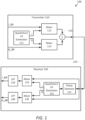
- FIG. 1 is a simplified diagram of a quadrature modulation transmission and reception system 100 according to some embodiments.
- quadrature modulation transmission and reception system 100 includes a transmitter 110 coupled to a receiver 130 via a transmission medium 120.
- transmission medium 120 may be wireless and/or include one or more conductors and/or one or more wave guides.
- transmitter 110 may be part of a larger transmission unit and receiver 130 may be part of a larger receiver unit.
- Transmitter 110 is designed to receive two quadrature baseband signals, I_BB and Q_BB, and generate a composite signal for transmission.
- a quadrature LO generator 111 generates both an in-phase (I) and quadrature (Q) LO signal at a desired LO frequency.
- the in-phase and quadrature LO signals are typically sinusoids at the desired LO frequency and have the same amplitude and a 90 degree phase difference.
- Data signal I_BB and the in-phase LO signal are passed to a mixer 112.
- Mixer 112 up-converts data signal I_BB to the in-phase LO signal.
- the resulting modulated in-phase signal is then passed to summer 114.
- mixer 112 may be a signal multiplier.
- data signal Q_BB and the quadrature LO signal are passed to a mixer 113.
- Mixer 113 up-convers data signal Q_BB to the quadrature LO signal.
- the resulting modulated quadrature signal is then passed to summer 114.
- mixer 113 may be a signal multiplier.
- Summer 114 adds the modulated in-phase signal and the modulated quadrature signal together to form a composite signal that is transmitted via an antenna. Due to imperfections in the quadrature LO signal, the composite signal typically includes both a desired sideband component and an undesired image component. For acceptable recovery of the I_BB and Q_BB data signals at a receiver, the undesired image has to be low enough to meet spectral mask specifications.
- phase detector 131 examines the composite signal and generates a phase reference that can be used to synchronize the phases of the in-phase and quadrature LO signals as generated in transmitter 110 by quadrature LO generator 111 and the in-phase and quadrature LO signals generated in receiver 130 by quadrature LO generator 132. This synchronization accounts for any phase shift introduced in transmitter 110, transmission medium 120, and/or receiver 130.
- phase detector 131 may further include a frequency offset to account for Doppler frequency shifts due to relative motion between transmitter 110 and receiver 130.
- Quadrature LO generator 132 generates both an in-phase (I) and quadrature (Q) LO signals at the desired frequency with a synchronizing phase shift provided by phase detector 131.
- the in-phase and quadrature LO signals are typically sinusoids at the desired frequency and have the same amplitude and a 90 degree phase difference.
- the in-phase LO signal provided by quadrature LO generator 132 is passed to mixer 133 where it is mixed with the composite signal received at receiver 130.
- Mixer 133 typically multiplies the received composite signal and the in-phase LO signal and generates a recovered version of I_BB and a signal at twice the desired frequency.
- the signal at twice the desired frequency is removed by low-pass filter 134 leaving the recovered version of the in-phase data signal I_BB'.
- quadrature LO signal provided by quadrature LO generator 132 is passed to mixer 135 where it is mixed with the composite signal received at receiver 130.
- Mixer 135 typically multiplies the received composite signal and the quadrature LO signal and generates a recovered version of Q_BB and a signal at twice the desired frequency.
- the signal at twice the desired frequency is removed by low-pass filter 136 leaving the recovered version of the quadrature data signal Q_BB'.
- the recovered version of the data signal I_BB' and the original version of the data signal I_BB are the same and the recovered version of the data signal Q_BB' and the original version of the data signal Q_BB are the same.
- imperfections in the modulation of transmitter 110 and the demodulation of receiver 130 result in differences between the recovered and original versions of the data signals.
- a good amplitude balance corresponds to the magnitudes of the in-phase and quadrature LO signals remaining equal or nearly equal.
- a good amplitude balance corresponds to the magnitudes of the in-phase and quadrature LO signals being within 0.3dB of each other.
- a good phase balance corresponds to maintaining the phase shift between the in-phase and quadrature LO signals at or close to 90 degrees.
- a good phase balance corresponds to the phase between the in-phase and quadrature LO signals staying within 83 and 93 degrees of each other.
- quadrature LO generators 111 and 132 plays an important role in the ability of quadrature modulation transmission and reception system 100 to successfully recover data signals I_BB and Q_BB at receiver 130.
- FIG. 2 is a simplified diagram of a quadrature LO generator 200 according to some embodiments.
- quadrature LO generator 200 may be used for quadrature LO generator 111 and/or 132 from Figure 1 .
- quadrature LO generator 200 includes a frequency synthesizer 210 and an in-phase/quadrature signal generator (IQ generator) 220.
- Frequency synthesizer 210 generates a local oscillator (LO) signal at a suitable frequency.
- the suitable frequency is twice the desired LO frequency for the in-phase and quadrature LO signals.
- frequency synthesizer 210 may include a phase-locked loop (PLL) or other similarly functioning circuitry to generate the LO signal.
- PLL phase-locked loop
- the LO signal is passed to IQ generator 220 to generate the in-phase (I) and quadrature (Q) LO signals.
- IQ generator 220 may be used by IQ generator 220 to generate the in-phase and quadrature LO signals from the LO signal.
- FIG 3 is a simplified diagram of a frequency divider 300 according to some embodiments.
- frequency divider 300 may be used as part of IQ generator 220. As shown in Figure 3 , frequency divider 300 receives an input signal have a frequency of twice the desired LO frequency and generates both an in-phase (I) LO signal and a quadrature (Q) LO signal at the desired LO frequency.
- I in-phase
- Q quadrature
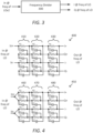
- FIG. 4 is a simplified diagram of polyphase filters 400 and 450 according to some embodiments.
- polyphase filters 400 and/or 450 may be used as part of IQ generator 220.
- polyphase filter 400 receives a signal at the desired LO frequency and is built around a multi-stage RC filtering network.
- Each of the n stages includes a similarly interconnected set of four same valued resistors (shown as Ri in stage i) and four capacitors (shown as Ci in stage i), although the resistor and capacitor values may be different in different stages.
- Stage 410 is the input stage for polyphase filter 400.
- a first resister includes a first terminal connected to a first side of an input signal (e.g., from one side of a frequency synthesizer, such as frequency synthesizer 210, that generates a differential output) and a second terminal connected to a first output of stage 410.
- a first capacitor includes a first terminal connected to the first terminal of the first resistor and a second terminal connected to a second output of stage 410.
- a second resistor includes a first terminal connected to a first terminal of a second capacitor. A second terminal of the second resistor is connected to the second terminal of the first capacitor and the second output of stage 410. The second terminal of the second capacitor is connected to a third output of stage 410.
- a third resister includes a first terminal connected to a second side of the input signal and a second terminal connected to the second terminal of the second capacitor and the third output of stage 410.
- a third capacitor includes a first terminal connected to the first terminal of the third resistor and a second terminal connected to a fourth output of stage 410.
- a fourth resistor includes a first terminal connected to a first terminal of a fourth capacitor.
- a second terminal of the fourth resistor is connected to the second terminal of the third capacitor and the fourth output of stage 410.
- the second terminal of the fourth capacitor is connected to the second terminal of the first resistor and the first output of stage 410.
- the interconnections among the resistors and capacitors of stage 420 are similar to that of stage 410 except that the first terminals of the first resistor and first capacitor are a first input for stage 420 connected to the first output of stage 410, the first terminals of the second resistor and second capacitor are a second input for stage 420 connected to the second output of stage 410, the first terminals of the third resistor and third capacitor are a third input for stage 420 connected to the third output of stage 410, and the first terminals of the fourth resistor and fourth capacitor are a fourth input for stage 420 connected to the fourth output of stage 410.
- stage 420 Subsequent stages of polyphase filter 400 are connected similar to stage 420 with the first through fourth inputs of the stage being connected to the first through fourth outputs, respectively, of the previous stage.
- the first and third outputs of the last (nth) stage 430 are the differential outputs (I+ and I-) of the in-phase LO signal, and the second and fourth outputs of stage 430 are the different outputs (Q+ and Q-) of the quadrature LO signal.
- Polyphase filter 450 similarly receives a signal at the desired frequency and includes n stages (shown via representative stages 460, 470, and 480).
- the internal interconnection of resistors and capacitors in polyphase filter 450 is similar to the internal interconnections of resistors and capacitors in polyphase filter 400.
- Polyphase filter 450 differs from polyphase filter 400 in that the first side of the input signal is connected to the first terminals of the first resistor, the first capacitor, the second resistor, and the second capacitor and the second side of the input signal is connected to the first terminals of the third resistor, the third capacitor, the fourth resistor, and the fourth capacitor.
- frequency divider 300 In practice, none of frequency divider 300, polyphase filter 400, and polyphase filter 450 is flexible enough to support a quadrature modulation transmission and reception system, such as quadrature modulation transmission and reception system 100, over a broad range of possible LO frequencies and with reasonable power consumption.
- a quadrature modulation transmission and reception system that is designed to flexibly operate with LO frequencies in the range of 0.5 GHz to 3 GHz may not be able to operate effectively across this broad range of LO frequencies using just a frequency divider or a polyphase filter.
- frequency divider 300 begins to exhibit poor amplitude and phase balance above 1.15 GHz and especially above 2 GHz. And although some improvements in amplitude and phase balance are possible by increasing the power used by frequency divider 300, the frequency range is still practicably limited to less than 2 GHz.
- polyphase filters 400 and 450 exhibit better amplitude and phase balance at frequencies above 1 GHz, but have a poor amplitude and phase balance at lower frequencies.
- polyphase filter 400 further provides good phase balance across a wide range in frequencies, but has an amplitude balance that deteriorates as the desired LO frequency diverges from the RC pole frequencies of stages 410-430.
- polyphase filter 450 further provides good amplitude balance across a wide range in frequencies, but has a phase balance that deteriorates as the desired LO frequency diverges from the RC pole frequencies of stages 460-480.
- a broad frequency range quadrature modulation transmission and reception system is not practical using frequency dividers or polyphase filters alone.
- a hybrid approach using both a frequency divider and a polyphase filter is able to provide both good amplitude and good phase balance across a full range of LO frequencies, such as those between 0.5 Hz and 3 GHz.
- the choice of whether to use the frequency divider or the polyphase filter to generate the in-phase and quadrature LO signals is made based on the desired LO frequency.
- the frequency divider is used for lower desired LO frequencies (e.g., from 0.5 GHz up to and including 1.15 GHz) and the polyphase filter is used for higher desired LO frequencies (e.g., from 1.15 GHz up to and including 3 GHz).
- the hybrid approach may have the added advantage of providing an analog-only solution to the generation of in-phase and quadrature LO signals with good amplitude and phase balance.
- FIG. 5 is a simplified diagram of a quadrature LO generator 500 according to some embodiments.
- quadrature LO generator 500 may be used for quadrature LO generator 111 and/or 132 from Figure 1 .
- quadrature LO generator 500 includes a frequency synthesizer 510. Similar to frequency synthesizer 210, frequency synthesizer 510 generates a differential local oscillator (LO) signal at a suitable frequency, which is shown in Figure 5 as a differential signal.
- LO local oscillator
- the frequency is selected based on a desired LO frequency for a corresponding transmitter or receiver and may alternatively be selected by an operator, a processor circuit (not shown), and/or some other suitable method as indicated by the frequency select input of frequency synthesizer 510.
- the frequency is either the desired LO frequency, when a polyphase filter 530 is used to generate the in-phase and quadrature LO signals, or twice the desired LO frequency, when a frequency divider 540 is used to generate the in-phase and quadrature LO signals.
- frequency synthesizer 510 may include a phase-locked loop (PLL) or other similarly functioning circuitry to generate the LO signal. The LO signal is then passed to low-pass filter 520 and frequency divider 540.
- PLL phase-locked loop
- Low-pass filter 520 is used to remove higher harmonics from the LO signal.
- the cut-off frequency of low-pass filter 520 may be approximately 1.5x the frequency of the primary frequency of the LO signal.
- low-pass filter 520 may be a first, second, or higher-order filter.
- low-pass filter 520 may be a passive or an active filter.
- low-pass filter 520 may be an elliptical filter, a Butterworth filter, a Chebyshev filter, a Bessel filter, a Cauer filter, and/or the like.
- the filtered LO signal is passed to a polyphase filter 530.
- Polyphase filter 530 receives the filtered LO signal and generates differential candidate in-phase (I 1 ) and quadrature (Q 1 ) LO signals.
- polyphase filter 530 is consistent with polyphase filter 400 and/or polyphase filter 450.
- the I 1 and Q 1 candidate in-phase and quadrature LO signals are then passed to a LO signal selector 550.
- the I 1 and Q 1 candidate in-phase and quadrature LO signals are suitable for use at higher frequencies, such as frequencies at or above 1.15 GHz.
- Frequency divider 540 receives the LO signal and generates differential candidate in-phase (I 2 ) and quadrature (Q 2 ) LO signals. In some examples, frequency divider 540 is consistent with frequency divider 300. The I 2 and Q 2 candidate in-phase and quadrature LO signals are then passed to LO signal selector 550. In some examples, the I 2 and Q 2 candidate in-phase and quadrature LO signals are suitable for use at lower frequencies, such as frequencies at or below 1.15 GHz.
- LO signal selector 550 is used to select between the I 1 and Q 1 and the I 2 and Q 2 candidate in-phase and quadrature LO signals to provide I and Q in-phase and quadrature LO signals (e.g., as differential LO signals) to other parts of a quadrature system.
- LO signal selector 550 uses the frequency select input that is also supplied to frequency synthesizer 510 to determine whether quadrature LO generator 500 is operating at low frequencies or high frequencies.
- the low frequencies may correspond to frequencies at or below 1.15 GHz and high frequencies may correspond to frequencies above 1.15 GHz.
- LO signal selector 550 determines that quadrature LO generator 500 is operating at high frequencies, the I 1 and Q 1 candidate in-phase and quadrature LO signals are selected as the in-phase and quadrature LO signals supplied as I and Q, respectively.
- the I 2 and Q 2 candidate in-phase and quadrature LO signals are selected as the in-phase and quadrature LO signals supplied as I and Q, respectively.
- LO signal selector 550 may include one or more multiplexors for selecting between the candidate in-phase and quadrature LO signals.
- LO signal selector 550 may include a frequency detector and comparator that determines which of the in-phase and quadrature LO signals from polyphase filter 530 (I 1 and Q 1 ) or the in-phase and quadrature LO signals from frequency divider 540 (I 2 and Q 2 ) based on the observed frequencies of one or more of the candidate in-phase and quadrature LO signals.
- the use of the frequency detector and comparator may eliminate the frequency select input on LO signal selector 550.
- quadrature LO generator 500 may operate in a reduced power mode.
- the reduced power mode may include disabling low-pass filter 520 and/or polyphase filter 530 when quadrature LO generator 500 is generating the in-phase and quadrature LO signals at low frequency and/or disabling frequency divider 540 when quadrature LO generator 500 is generating the in-phase and quadrature LO signals at high frequency.
Landscapes
- Engineering & Computer Science (AREA)
- Signal Processing (AREA)
- Computer Networks & Wireless Communication (AREA)
- Power Engineering (AREA)
- Transmitters (AREA)
- Digital Transmission Methods That Use Modulated Carrier Waves (AREA)
- Stabilization Of Oscillater, Synchronisation, Frequency Synthesizers (AREA)
Claims (15)
- Schaltung zum Erzeugen von Quadratur-Lokaloszillatorsignalen, LO-Signalen, wobei die Schaltung umfasst:einen Frequenzsynthesizer (510), der ein erstes LO-Signal erzeugt;ein Mehrphasenfilter (530), das zum Empfangen des ersten LO-Signals gekoppelt ist und Erzeugen eines ersten phasengleichen LO-Signals und eines ersten Quadratur-LO-Signals;einen Frequenzteiler (540), der gekoppelt ist, um das erste LO-Signal zu empfangen und ein zweites phasengleiches LO-Signal und ein zweites Quadratur-LO-Signal zu erzeugen; wobei die Schaltung dadurch gekennzeichnet ist, dass sie ferner umfasst:
einen LO-Signalselektor (550) zum Auswählen entweder des ersten oder des zweiten phasengleichen LO-Signals als ein phasengleiches LO-Ausgangssignal und zum Auswählen entweder des ersten oder des zweiten Quadratur-LO-Signals als ein Quadratur-LO-Ausgangssignal basierend auf einer gewünschten Ausgangsfrequenz, die durch ein Frequenzauswahlsignal angegeben wird, das zum Einstellen einer Frequenz des ersten LO-Signals verwendet wird. - Schaltung nach Anspruch 1, die ferner ein Tiefpassfilter umfasst, das zwischen dem Frequenzsynthesizer und dem Mehrphasenfilter geschaltet ist.
- Schaltung nach Anspruch 1, wobei der LO-Signalselektor:das erste phasengleiche LO-Signal als phasengleiches LO-Ausgangssignal auswählt, wenn die gewünschte Ausgangsfrequenz über einer Schwellenfrequenz liegt;das erste Quadratur-LO-Signal als Ausgangs-Quadratur-LO-Signal auswählt, wenn die gewünschte Ausgangsfrequenz über der Schwellenfrequenz liegt;das zweite phasengleiche LO-Signal als phasengleiches LO-Ausgangssignal auswählt, wenn die gewünschte Ausgangsfrequenz bei oder unter der Schwellenfrequenz liegt; unddas zweite Quadratur-LO-Signal als Ausgangs-Quadratur-LO-Signal auswählt, wenn die gewünschte Ausgangsfrequenz bei oder unter der Schwellenfrequenz liegt.
- Schaltungen Anspruch 3, wobei die Schwellenfrequenz 1,15 GHz ist.
- Schaltung nach Anspruch 1, wobei die gewünschte Ausgangsfrequenz basierend auf einem Frequenzauswahlsignal bestimmt wird, das dem LO-Signalselektor bereitgestellt wird.
- Schaltung nach Anspruch 5, wobei das Frequenzauswahlsignal dem Frequenzsynthesizer bereitgestellt wird, um eine Frequenz des ersten LO-Signals einzustellen.
- Schaltung nach Anspruch 1, wobei der LO-Signalselektor einen oder mehrere Multiplexer umfasst.
- Schaltung nach Anspruch 1, wobei der LO-Signalselektor einen Frequenzdetektor zum Bestimmen der gewünschten Ausgangsfrequenz basierend auf einer Frequenz des ersten phasengleichen LO-Signals, einer Frequenz des zweiten phasengleichen LO-Signals, einer Frequenz des ersten Quadratur-LO-Signals oder einer Frequenz des zweiten Quadratur-LO-Signals umfasst.
- Schaltung nach Anspruch 1, wobei das phasengleiche LO-Ausgangssignal und das Quadratur-LO-Ausgangssignal annähernd die gleiche Amplitude und eine Phasenverschiebung von annähernd 90 Grad aufweisen, wenn die gewünschte Ausgangsfrequenz innerhalb eines Bereichs von Betriebsfrequenzen für die Schaltung liegt.
- Schaltung nach Anspruch 9, wobei sich der Bereich der Betriebsfrequenzen von 0,5 GHz bis 3 GHz erstreckt.
- Verfahren zum Erzeugen von Quadratur-Lokaloszillatorsignalen, LO-Signalen, wobei das Verfahren umfasst:Erzeugen eines ersten LO-Signals;unter Verwendung eines Mehrphasenfilters (530) und des ersten LO-Signals Erzeugen eines ersten phasengleichen LO-Signals und eines ersten Quadratur-LO-Signals;unter Verwendung eines Frequenzteilers (540) und des ersten LO-Signals Erzeugen eines zweiten phasengleichen LO-Signals und eines zweiten Quadratur-LO-Signals; wobei das Verfahren dadurch gekennzeichnet ist, dass es ferner einen folgenden Schritt umfasst:
Auswählen entweder des ersten oder des zweiten phasengleichen LO-Signals als ein phasengleiches LO-Ausgangssignal und Auswählen entweder des ersten oder des zweiten Quadratur-LO-Signals als ein Quadratur-LO-Ausgangssignal basierend auf einer gewünschten Ausgangsfrequenz, die durch ein Frequenzauswahlsignal angegeben wird, das zum Einstellen einer Frequenz des ersten LO-Signals verwendet wird. - Verfahren nach Anspruch 11, wobei das Auswählen umfasst:Auswählen des ersten phasengleichen LO-Signals als phasengleiches LO-Ausgangssignal, wenn die gewünschte Ausgangsfrequenz über einer Schwellenfrequenz liegt;Auswählen des ersten Quadratur-LO-Signals als Ausgangs-Quadratur-LO-Signal, wenn die gewünschte Ausgangsfrequenz über der Schwellenfrequenz liegt;Auswählen des zweiten phasengleichen LO-Signals als das phasengleiche LO-Ausgangssignal, wenn die gewünschte Ausgangsfrequenz bei oder unter der Schwellenfrequenz liegt; undAuswählen des zweiten Quadratur-LO-Signals als Ausgangs-Quadratur-LO-Signal, wenn die gewünschte Ausgangsfrequenz bei oder unter der Schwellenfrequenz liegt.
- Verfahren nach Anspruch 11, das ferner eine Tiefpassfilterung des ersten LO-Signals umfasst, bevor es dem Mehrphasenfilter bereitgestellt wird.
- Verfahren nach Anspruch 11, das ferner das Deaktivieren des Mehrphasenfilters oder des Frequenzteilers basierend auf der gewünschten Ausgangsfrequenz umfasst.
- Verfahren nach Anspruch 11, wobei das phasengleiche LO-Ausgangssignal und das Quadratur-LO-Ausgangssignal eine gute Amplitudenbalance und eine gute Phasenbalance aufweisen, wenn die gewünschte Ausgangsfrequenz innerhalb eines Betriebsfrequenzbereichs liegt, der sich von 0,5 GHz bis 3 GHz erstreckt.
Applications Claiming Priority (2)
| Application Number | Priority Date | Filing Date | Title |
|---|---|---|---|
| US15/632,093 US10389572B2 (en) | 2017-06-23 | 2017-06-23 | Circuits and systems for wideband quadrature signal generation |
| PCT/US2018/039074 WO2018237309A1 (en) | 2017-06-23 | 2018-06-22 | Circuits and systems for wideband quadrature signal generation |
Publications (3)
| Publication Number | Publication Date |
|---|---|
| EP3642995A1 EP3642995A1 (de) | 2020-04-29 |
| EP3642995A4 EP3642995A4 (de) | 2021-03-17 |
| EP3642995B1 true EP3642995B1 (de) | 2023-03-08 |
Family
ID=64693781
Family Applications (1)
| Application Number | Title | Priority Date | Filing Date |
|---|---|---|---|
| EP18819800.6A Active EP3642995B1 (de) | 2017-06-23 | 2018-06-22 | Schaltungen und systeme zur breitbandquadratursignalerzeugung |
Country Status (5)
| Country | Link |
|---|---|
| US (2) | US10389572B2 (de) |
| EP (1) | EP3642995B1 (de) |
| KR (1) | KR20200015784A (de) |
| CN (1) | CN110785959B (de) |
| WO (1) | WO2018237309A1 (de) |
Families Citing this family (4)
| Publication number | Priority date | Publication date | Assignee | Title |
|---|---|---|---|---|
| US10734967B2 (en) * | 2018-09-28 | 2020-08-04 | Apple Inc. | Capacitor compensated dual of polyphase filter |
| US11271597B1 (en) * | 2020-09-15 | 2022-03-08 | Swiftlink Technologies Co., Ltd. | Wideband transmitter for millimeter-wave wireless communication |
| US12596081B2 (en) * | 2021-11-30 | 2026-04-07 | Arizona Board Of Regents On Behalfof Arizona State University | Compact, low-power, high image rejection sideband separation receiver |
| US12328099B2 (en) | 2023-02-23 | 2025-06-10 | Analog Devices, Inc. | Apparatus and methods for local oscillator interface circuits with quadrature clock generation and phase correction |
Family Cites Families (18)
| Publication number | Priority date | Publication date | Assignee | Title |
|---|---|---|---|---|
| JPS589422A (ja) * | 1981-07-10 | 1983-01-19 | Hitachi Ltd | 選局装置 |
| US4593257A (en) * | 1985-02-28 | 1986-06-03 | Rca Corporation | Multiband local oscillator |
| US6058291A (en) * | 1997-12-03 | 2000-05-02 | 3Com Corporation | Methods and apparatus for carrier suppression in a radio modulator |
| US6169463B1 (en) * | 1999-03-24 | 2001-01-02 | Philips Electronic North America Corp. | Quadrature modulator with set-and-forget carrier leakage compensation |
| US7555263B1 (en) * | 1999-10-21 | 2009-06-30 | Broadcom Corporation | Adaptive radio transceiver |
| US7095454B2 (en) * | 2003-07-30 | 2006-08-22 | Maxim Integrated Products, Inc. | Broadband single conversion tuner integrated circuits |
| US7362826B2 (en) * | 2003-09-29 | 2008-04-22 | Silicon Laboratories, Inc. | Receiver including an oscillation circuit for generating an image rejection calibration tone |
| EP1792394A1 (de) * | 2004-09-14 | 2007-06-06 | Koninklijke Philips Electronics N.V. | Einrichtung zur ultrabreitbandigen frequenzerzeugung |
| US7912429B2 (en) * | 2005-09-06 | 2011-03-22 | Mediatek, Inc. | LO 2LO upconverter for an in-phase/quadrature-phase (I/Q) modulator |
| US7321268B2 (en) * | 2005-11-04 | 2008-01-22 | Via Technologies | Ultra wideband and fast hopping frequency synthesizer for MB-OFDM wireless application |
| US7809338B2 (en) * | 2006-08-29 | 2010-10-05 | Texas Instruments Incorporated | Local oscillator with non-harmonic ratio between oscillator and RF frequencies using wideband modulation spectral replicas |
| CA2639568C (en) * | 2007-09-14 | 2014-05-13 | Mohammad Reza Nezhad Ahmadi Mohabadi | Low-if transceiver architecture |
| JP5623279B2 (ja) * | 2007-09-28 | 2014-11-12 | アギア システムズ エルエルシーAgere Systems LLC | 拡張されたトラッキング範囲を有する位相ロック・ループ(pll) |
| US8509208B2 (en) * | 2008-02-01 | 2013-08-13 | Qualcomm Incorporated | Frequency error estimation |
| KR101271425B1 (ko) * | 2009-12-15 | 2013-06-05 | 한국전자통신연구원 | 듀얼밴드 광대역 국부신호 발생장치 |
| US8508308B2 (en) * | 2011-09-01 | 2013-08-13 | Lsi Corporation | Automatic frequency calibration of a multi-LCVCO phase locked loop with adaptive thresholds and programmable center control voltage |
| TWI513195B (zh) * | 2012-04-24 | 2015-12-11 | Mstar Semiconductor Inc | 震盪信號提供器、同相與正交震盪信號提供器以及相關之信號處理方法 |
| US9559792B1 (en) * | 2015-08-31 | 2017-01-31 | Xillinx, Inc. | Broadband in-phase and quadrature phase signal generation |
-
2017
- 2017-06-23 US US15/632,093 patent/US10389572B2/en active Active
-
2018
- 2018-06-22 EP EP18819800.6A patent/EP3642995B1/de active Active
- 2018-06-22 WO PCT/US2018/039074 patent/WO2018237309A1/en not_active Ceased
- 2018-06-22 CN CN201880042144.XA patent/CN110785959B/zh active Active
- 2018-06-22 KR KR1020207001982A patent/KR20200015784A/ko not_active Ceased
-
2019
- 2019-08-16 US US16/543,373 patent/US20190372823A1/en not_active Abandoned
Also Published As
| Publication number | Publication date |
|---|---|
| US20190372823A1 (en) | 2019-12-05 |
| EP3642995A1 (de) | 2020-04-29 |
| EP3642995A4 (de) | 2021-03-17 |
| CN110785959A (zh) | 2020-02-11 |
| KR20200015784A (ko) | 2020-02-12 |
| US20180375711A1 (en) | 2018-12-27 |
| WO2018237309A1 (en) | 2018-12-27 |
| US10389572B2 (en) | 2019-08-20 |
| CN110785959B (zh) | 2021-07-30 |
Similar Documents
| Publication | Publication Date | Title |
|---|---|---|
| JP4236059B2 (ja) | 周波数変換回路 | |
| EP3642995B1 (de) | Schaltungen und systeme zur breitbandquadratursignalerzeugung | |
| US5819161A (en) | Two way radio set utilizing a single oscillator | |
| EP2805424A1 (de) | Funkfrequenzempfänger mit doppelter umwandlung und zwei trägern | |
| US7454185B2 (en) | Wideband I/Q signal generation device | |
| EP1178604B1 (de) | System zur Frequenzumsetzung von FM-Signalen | |
| CA2771958C (en) | Unified frequency synthesizer for direct conversion receiver or transmitter | |
| US5642385A (en) | Frequency detector for carrier frequency synchronization | |
| JP4851458B2 (ja) | 装置、発振段、周波数選択器、システム、方法 | |
| JP3256422B2 (ja) | 周波数シンセサイザ | |
| US9042486B2 (en) | Sideband suppression in angle modulated signals | |
| US10594342B1 (en) | Power amplifying system and associated power amplifying method for bluetooth device | |
| US20050243948A1 (en) | Frequency shift keying modulator and applications thereof | |
| US7817977B1 (en) | Configurable signal generator | |
| EP1575179A2 (de) | Verfahren und Schaltung zur Demodulation | |
| JPH0541717A (ja) | デジタル変調波の復調装置 | |
| KR20020000895A (ko) | 통신 시스템 | |
| CN104242922B (zh) | 无线通信设备及其频率合成装置 | |
| JP2919328B2 (ja) | 変調回路 | |
| US20030067357A1 (en) | Automatic multiple II/4 phase shifter | |
| JPH0541718A (ja) | デジタル変調波の復調装置 | |
| US9391562B2 (en) | Local oscillation generator, associated communication system and method for local oscillation generation | |
| JP3462277B2 (ja) | 搬送波再生回路 | |
| JP2002353835A (ja) | 受信器 | |
| JPS63260247A (ja) | 変調器 |
Legal Events
| Date | Code | Title | Description |
|---|---|---|---|
| STAA | Information on the status of an ep patent application or granted ep patent |
Free format text: STATUS: THE INTERNATIONAL PUBLICATION HAS BEEN MADE |
|
| PUAI | Public reference made under article 153(3) epc to a published international application that has entered the european phase |
Free format text: ORIGINAL CODE: 0009012 |
|
| STAA | Information on the status of an ep patent application or granted ep patent |
Free format text: STATUS: REQUEST FOR EXAMINATION WAS MADE |
|
| 17P | Request for examination filed |
Effective date: 20200116 |
|
| AK | Designated contracting states |
Kind code of ref document: A1 Designated state(s): AL AT BE BG CH CY CZ DE DK EE ES FI FR GB GR HR HU IE IS IT LI LT LU LV MC MK MT NL NO PL PT RO RS SE SI SK SM TR |
|
| AX | Request for extension of the european patent |
Extension state: BA ME |
|
| DAV | Request for validation of the european patent (deleted) | ||
| DAX | Request for extension of the european patent (deleted) | ||
| A4 | Supplementary search report drawn up and despatched |
Effective date: 20210217 |
|
| RIC1 | Information provided on ipc code assigned before grant |
Ipc: H04B 17/12 20150101ALI20210211BHEP Ipc: H04L 5/12 20060101AFI20210211BHEP Ipc: H04L 27/26 20060101ALI20210211BHEP |
|
| REG | Reference to a national code |
Ref country code: DE Ref legal event code: R079 Ref document number: 602018047054 Country of ref document: DE Free format text: PREVIOUS MAIN CLASS: H04L0005120000 Ipc: H03B0027000000 |
|
| GRAP | Despatch of communication of intention to grant a patent |
Free format text: ORIGINAL CODE: EPIDOSNIGR1 |
|
| STAA | Information on the status of an ep patent application or granted ep patent |
Free format text: STATUS: GRANT OF PATENT IS INTENDED |
|
| RIC1 | Information provided on ipc code assigned before grant |
Ipc: H04L 27/00 20060101ALI20220902BHEP Ipc: H04L 23/02 20060101ALI20220902BHEP Ipc: H03D 7/16 20060101ALI20220902BHEP Ipc: H03C 3/00 20060101ALI20220902BHEP Ipc: H03B 27/00 20060101AFI20220902BHEP |
|
| INTG | Intention to grant announced |
Effective date: 20220929 |
|
| GRAS | Grant fee paid |
Free format text: ORIGINAL CODE: EPIDOSNIGR3 |
|
| GRAA | (expected) grant |
Free format text: ORIGINAL CODE: 0009210 |
|
| STAA | Information on the status of an ep patent application or granted ep patent |
Free format text: STATUS: THE PATENT HAS BEEN GRANTED |
|
| AK | Designated contracting states |
Kind code of ref document: B1 Designated state(s): AL AT BE BG CH CY CZ DE DK EE ES FI FR GB GR HR HU IE IS IT LI LT LU LV MC MK MT NL NO PL PT RO RS SE SI SK SM TR |
|
| REG | Reference to a national code |
Ref country code: CH Ref legal event code: EP Ref country code: AT Ref legal event code: REF Ref document number: 1553277 Country of ref document: AT Kind code of ref document: T Effective date: 20230315 |
|
| REG | Reference to a national code |
Ref country code: DE Ref legal event code: R096 Ref document number: 602018047054 Country of ref document: DE |
|
| REG | Reference to a national code |
Ref country code: IE Ref legal event code: FG4D |
|
| REG | Reference to a national code |
Ref country code: LT Ref legal event code: MG9D |
|
| REG | Reference to a national code |
Ref country code: NL Ref legal event code: MP Effective date: 20230308 |
|
| PG25 | Lapsed in a contracting state [announced via postgrant information from national office to epo] |
Ref country code: RS Free format text: LAPSE BECAUSE OF FAILURE TO SUBMIT A TRANSLATION OF THE DESCRIPTION OR TO PAY THE FEE WITHIN THE PRESCRIBED TIME-LIMIT Effective date: 20230308 Ref country code: NO Free format text: LAPSE BECAUSE OF FAILURE TO SUBMIT A TRANSLATION OF THE DESCRIPTION OR TO PAY THE FEE WITHIN THE PRESCRIBED TIME-LIMIT Effective date: 20230608 Ref country code: LV Free format text: LAPSE BECAUSE OF FAILURE TO SUBMIT A TRANSLATION OF THE DESCRIPTION OR TO PAY THE FEE WITHIN THE PRESCRIBED TIME-LIMIT Effective date: 20230308 Ref country code: LT Free format text: LAPSE BECAUSE OF FAILURE TO SUBMIT A TRANSLATION OF THE DESCRIPTION OR TO PAY THE FEE WITHIN THE PRESCRIBED TIME-LIMIT Effective date: 20230308 Ref country code: HR Free format text: LAPSE BECAUSE OF FAILURE TO SUBMIT A TRANSLATION OF THE DESCRIPTION OR TO PAY THE FEE WITHIN THE PRESCRIBED TIME-LIMIT Effective date: 20230308 Ref country code: ES Free format text: LAPSE BECAUSE OF FAILURE TO SUBMIT A TRANSLATION OF THE DESCRIPTION OR TO PAY THE FEE WITHIN THE PRESCRIBED TIME-LIMIT Effective date: 20230308 |
|
| REG | Reference to a national code |
Ref country code: AT Ref legal event code: MK05 Ref document number: 1553277 Country of ref document: AT Kind code of ref document: T Effective date: 20230308 |
|
| PG25 | Lapsed in a contracting state [announced via postgrant information from national office to epo] |
Ref country code: SE Free format text: LAPSE BECAUSE OF FAILURE TO SUBMIT A TRANSLATION OF THE DESCRIPTION OR TO PAY THE FEE WITHIN THE PRESCRIBED TIME-LIMIT Effective date: 20230308 Ref country code: NL Free format text: LAPSE BECAUSE OF FAILURE TO SUBMIT A TRANSLATION OF THE DESCRIPTION OR TO PAY THE FEE WITHIN THE PRESCRIBED TIME-LIMIT Effective date: 20230308 Ref country code: GR Free format text: LAPSE BECAUSE OF FAILURE TO SUBMIT A TRANSLATION OF THE DESCRIPTION OR TO PAY THE FEE WITHIN THE PRESCRIBED TIME-LIMIT Effective date: 20230609 Ref country code: FI Free format text: LAPSE BECAUSE OF FAILURE TO SUBMIT A TRANSLATION OF THE DESCRIPTION OR TO PAY THE FEE WITHIN THE PRESCRIBED TIME-LIMIT Effective date: 20230308 |
|
| PG25 | Lapsed in a contracting state [announced via postgrant information from national office to epo] |
Ref country code: SM Free format text: LAPSE BECAUSE OF FAILURE TO SUBMIT A TRANSLATION OF THE DESCRIPTION OR TO PAY THE FEE WITHIN THE PRESCRIBED TIME-LIMIT Effective date: 20230308 Ref country code: RO Free format text: LAPSE BECAUSE OF FAILURE TO SUBMIT A TRANSLATION OF THE DESCRIPTION OR TO PAY THE FEE WITHIN THE PRESCRIBED TIME-LIMIT Effective date: 20230308 Ref country code: PT Free format text: LAPSE BECAUSE OF FAILURE TO SUBMIT A TRANSLATION OF THE DESCRIPTION OR TO PAY THE FEE WITHIN THE PRESCRIBED TIME-LIMIT Effective date: 20230710 Ref country code: EE Free format text: LAPSE BECAUSE OF FAILURE TO SUBMIT A TRANSLATION OF THE DESCRIPTION OR TO PAY THE FEE WITHIN THE PRESCRIBED TIME-LIMIT Effective date: 20230308 Ref country code: CZ Free format text: LAPSE BECAUSE OF FAILURE TO SUBMIT A TRANSLATION OF THE DESCRIPTION OR TO PAY THE FEE WITHIN THE PRESCRIBED TIME-LIMIT Effective date: 20230308 Ref country code: AT Free format text: LAPSE BECAUSE OF FAILURE TO SUBMIT A TRANSLATION OF THE DESCRIPTION OR TO PAY THE FEE WITHIN THE PRESCRIBED TIME-LIMIT Effective date: 20230308 |
|
| PG25 | Lapsed in a contracting state [announced via postgrant information from national office to epo] |
Ref country code: SK Free format text: LAPSE BECAUSE OF FAILURE TO SUBMIT A TRANSLATION OF THE DESCRIPTION OR TO PAY THE FEE WITHIN THE PRESCRIBED TIME-LIMIT Effective date: 20230308 Ref country code: PL Free format text: LAPSE BECAUSE OF FAILURE TO SUBMIT A TRANSLATION OF THE DESCRIPTION OR TO PAY THE FEE WITHIN THE PRESCRIBED TIME-LIMIT Effective date: 20230308 Ref country code: IS Free format text: LAPSE BECAUSE OF FAILURE TO SUBMIT A TRANSLATION OF THE DESCRIPTION OR TO PAY THE FEE WITHIN THE PRESCRIBED TIME-LIMIT Effective date: 20230708 |
|
| REG | Reference to a national code |
Ref country code: DE Ref legal event code: R097 Ref document number: 602018047054 Country of ref document: DE |
|
| PLBE | No opposition filed within time limit |
Free format text: ORIGINAL CODE: 0009261 |
|
| STAA | Information on the status of an ep patent application or granted ep patent |
Free format text: STATUS: NO OPPOSITION FILED WITHIN TIME LIMIT |
|
| PG25 | Lapsed in a contracting state [announced via postgrant information from national office to epo] |
Ref country code: MC Free format text: LAPSE BECAUSE OF FAILURE TO SUBMIT A TRANSLATION OF THE DESCRIPTION OR TO PAY THE FEE WITHIN THE PRESCRIBED TIME-LIMIT Effective date: 20230308 |
|
| PG25 | Lapsed in a contracting state [announced via postgrant information from national office to epo] |
Ref country code: SI Free format text: LAPSE BECAUSE OF FAILURE TO SUBMIT A TRANSLATION OF THE DESCRIPTION OR TO PAY THE FEE WITHIN THE PRESCRIBED TIME-LIMIT Effective date: 20230308 Ref country code: MC Free format text: LAPSE BECAUSE OF FAILURE TO SUBMIT A TRANSLATION OF THE DESCRIPTION OR TO PAY THE FEE WITHIN THE PRESCRIBED TIME-LIMIT Effective date: 20230308 Ref country code: DK Free format text: LAPSE BECAUSE OF FAILURE TO SUBMIT A TRANSLATION OF THE DESCRIPTION OR TO PAY THE FEE WITHIN THE PRESCRIBED TIME-LIMIT Effective date: 20230308 |
|
| REG | Reference to a national code |
Ref country code: CH Ref legal event code: PL |
|
| 26N | No opposition filed |
Effective date: 20231211 |
|
| REG | Reference to a national code |
Ref country code: BE Ref legal event code: MM Effective date: 20230630 |
|
| GBPC | Gb: european patent ceased through non-payment of renewal fee |
Effective date: 20230622 |
|
| PG25 | Lapsed in a contracting state [announced via postgrant information from national office to epo] |
Ref country code: LU Free format text: LAPSE BECAUSE OF NON-PAYMENT OF DUE FEES Effective date: 20230622 |
|
| REG | Reference to a national code |
Ref country code: IE Ref legal event code: MM4A |
|
| PG25 | Lapsed in a contracting state [announced via postgrant information from national office to epo] |
Ref country code: LU Free format text: LAPSE BECAUSE OF NON-PAYMENT OF DUE FEES Effective date: 20230622 |
|
| PG25 | Lapsed in a contracting state [announced via postgrant information from national office to epo] |
Ref country code: IE Free format text: LAPSE BECAUSE OF NON-PAYMENT OF DUE FEES Effective date: 20230622 |
|
| PG25 | Lapsed in a contracting state [announced via postgrant information from national office to epo] |
Ref country code: IE Free format text: LAPSE BECAUSE OF NON-PAYMENT OF DUE FEES Effective date: 20230622 Ref country code: GB Free format text: LAPSE BECAUSE OF NON-PAYMENT OF DUE FEES Effective date: 20230622 Ref country code: CH Free format text: LAPSE BECAUSE OF NON-PAYMENT OF DUE FEES Effective date: 20230630 |
|
| PG25 | Lapsed in a contracting state [announced via postgrant information from national office to epo] |
Ref country code: IT Free format text: LAPSE BECAUSE OF FAILURE TO SUBMIT A TRANSLATION OF THE DESCRIPTION OR TO PAY THE FEE WITHIN THE PRESCRIBED TIME-LIMIT Effective date: 20230308 Ref country code: FR Free format text: LAPSE BECAUSE OF NON-PAYMENT OF DUE FEES Effective date: 20230630 Ref country code: BE Free format text: LAPSE BECAUSE OF NON-PAYMENT OF DUE FEES Effective date: 20230630 |
|
| PG25 | Lapsed in a contracting state [announced via postgrant information from national office to epo] |
Ref country code: BG Free format text: LAPSE BECAUSE OF FAILURE TO SUBMIT A TRANSLATION OF THE DESCRIPTION OR TO PAY THE FEE WITHIN THE PRESCRIBED TIME-LIMIT Effective date: 20230308 |
|
| PG25 | Lapsed in a contracting state [announced via postgrant information from national office to epo] |
Ref country code: BG Free format text: LAPSE BECAUSE OF FAILURE TO SUBMIT A TRANSLATION OF THE DESCRIPTION OR TO PAY THE FEE WITHIN THE PRESCRIBED TIME-LIMIT Effective date: 20230308 |
|
| PGFP | Annual fee paid to national office [announced via postgrant information from national office to epo] |
Ref country code: DE Payment date: 20250630 Year of fee payment: 8 |
|
| PG25 | Lapsed in a contracting state [announced via postgrant information from national office to epo] |
Ref country code: CY Free format text: LAPSE BECAUSE OF FAILURE TO SUBMIT A TRANSLATION OF THE DESCRIPTION OR TO PAY THE FEE WITHIN THE PRESCRIBED TIME-LIMIT; INVALID AB INITIO Effective date: 20180622 |
|
| REG | Reference to a national code |
Ref country code: DE Ref legal event code: R081 Ref document number: 602018047054 Country of ref document: DE Owner name: AXIRO SEMICONDUCTOR INC., SAN DIEGO, US Free format text: FORMER OWNER: INTEGRATED DEVICE TECHNOLOGY, INC., SAN JOSE, CA, US Ref country code: DE Ref legal event code: R081 Ref document number: 602018047054 Country of ref document: DE Owner name: AXIRO SEMICONDUCTOR INC., SAN DIEGO, US Free format text: FORMER OWNER: RENESAS ELECTRONICS AMERICA INC., MILPITAS, CA, US |
|
| PG25 | Lapsed in a contracting state [announced via postgrant information from national office to epo] |
Ref country code: HU Free format text: LAPSE BECAUSE OF FAILURE TO SUBMIT A TRANSLATION OF THE DESCRIPTION OR TO PAY THE FEE WITHIN THE PRESCRIBED TIME-LIMIT; INVALID AB INITIO Effective date: 20180622 |
|
| REG | Reference to a national code |
Ref country code: DE Ref legal event code: R082 Ref document number: 602018047054 Country of ref document: DE Representative=s name: TBK, DE |
|
| PG25 | Lapsed in a contracting state [announced via postgrant information from national office to epo] |
Ref country code: TR Free format text: LAPSE BECAUSE OF FAILURE TO SUBMIT A TRANSLATION OF THE DESCRIPTION OR TO PAY THE FEE WITHIN THE PRESCRIBED TIME-LIMIT Effective date: 20230308 |