EP3640976A1 - Mask and method for preparing array substrate - Google Patents
Mask and method for preparing array substrate Download PDFInfo
- Publication number
- EP3640976A1 EP3640976A1 EP17908931.3A EP17908931A EP3640976A1 EP 3640976 A1 EP3640976 A1 EP 3640976A1 EP 17908931 A EP17908931 A EP 17908931A EP 3640976 A1 EP3640976 A1 EP 3640976A1
- Authority
- EP
- European Patent Office
- Prior art keywords
- area
- sub
- photoresist
- areas
- mask plate
- Prior art date
- Legal status (The legal status is an assumption and is not a legal conclusion. Google has not performed a legal analysis and makes no representation as to the accuracy of the status listed.)
- Withdrawn
Links
Images
Classifications
-
- G—PHYSICS
- G03—PHOTOGRAPHY; CINEMATOGRAPHY; ANALOGOUS TECHNIQUES USING WAVES OTHER THAN OPTICAL WAVES; ELECTROGRAPHY; HOLOGRAPHY
- G03F—PHOTOMECHANICAL PRODUCTION OF TEXTURED OR PATTERNED SURFACES, e.g. FOR PRINTING, FOR PROCESSING OF SEMICONDUCTOR DEVICES; MATERIALS THEREFOR; ORIGINALS THEREFOR; APPARATUS SPECIALLY ADAPTED THEREFOR
- G03F1/00—Originals for photomechanical production of textured or patterned surfaces, e.g., masks, photo-masks, reticles; Mask blanks or pellicles therefor; Containers specially adapted therefor; Preparation thereof
- G03F1/54—Absorbers, e.g. of opaque materials
- G03F1/58—Absorbers, e.g. of opaque materials having two or more different absorber layers, e.g. stacked multilayer absorbers
-
- G—PHYSICS
- G03—PHOTOGRAPHY; CINEMATOGRAPHY; ANALOGOUS TECHNIQUES USING WAVES OTHER THAN OPTICAL WAVES; ELECTROGRAPHY; HOLOGRAPHY
- G03F—PHOTOMECHANICAL PRODUCTION OF TEXTURED OR PATTERNED SURFACES, e.g. FOR PRINTING, FOR PROCESSING OF SEMICONDUCTOR DEVICES; MATERIALS THEREFOR; ORIGINALS THEREFOR; APPARATUS SPECIALLY ADAPTED THEREFOR
- G03F1/00—Originals for photomechanical production of textured or patterned surfaces, e.g., masks, photo-masks, reticles; Mask blanks or pellicles therefor; Containers specially adapted therefor; Preparation thereof
- G03F1/54—Absorbers, e.g. of opaque materials
-
- G—PHYSICS
- G03—PHOTOGRAPHY; CINEMATOGRAPHY; ANALOGOUS TECHNIQUES USING WAVES OTHER THAN OPTICAL WAVES; ELECTROGRAPHY; HOLOGRAPHY
- G03F—PHOTOMECHANICAL PRODUCTION OF TEXTURED OR PATTERNED SURFACES, e.g. FOR PRINTING, FOR PROCESSING OF SEMICONDUCTOR DEVICES; MATERIALS THEREFOR; ORIGINALS THEREFOR; APPARATUS SPECIALLY ADAPTED THEREFOR
- G03F7/00—Photomechanical, e.g. photolithographic, production of textured or patterned surfaces, e.g. printing surfaces; Materials therefor, e.g. comprising photoresists; Apparatus specially adapted therefor
- G03F7/20—Exposure; Apparatus therefor
- G03F7/2051—Exposure without an original mask, e.g. using a programmed deflection of a point source, by scanning, by drawing with a light beam, using an addressed light or corpuscular source
- G03F7/2059—Exposure without an original mask, e.g. using a programmed deflection of a point source, by scanning, by drawing with a light beam, using an addressed light or corpuscular source using a scanning corpuscular radiation beam, e.g. an electron beam
- G03F7/2063—Exposure without an original mask, e.g. using a programmed deflection of a point source, by scanning, by drawing with a light beam, using an addressed light or corpuscular source using a scanning corpuscular radiation beam, e.g. an electron beam for the production of exposure masks or reticles
-
- G—PHYSICS
- G02—OPTICS
- G02F—OPTICAL DEVICES OR ARRANGEMENTS FOR THE CONTROL OF LIGHT BY MODIFICATION OF THE OPTICAL PROPERTIES OF THE MEDIA OF THE ELEMENTS INVOLVED THEREIN; NON-LINEAR OPTICS; FREQUENCY-CHANGING OF LIGHT; OPTICAL LOGIC ELEMENTS; OPTICAL ANALOGUE/DIGITAL CONVERTERS
- G02F1/00—Devices or arrangements for the control of the intensity, colour, phase, polarisation or direction of light arriving from an independent light source, e.g. switching, gating or modulating; Non-linear optics
- G02F1/01—Devices or arrangements for the control of the intensity, colour, phase, polarisation or direction of light arriving from an independent light source, e.g. switching, gating or modulating; Non-linear optics for the control of the intensity, phase, polarisation or colour
- G02F1/13—Devices or arrangements for the control of the intensity, colour, phase, polarisation or direction of light arriving from an independent light source, e.g. switching, gating or modulating; Non-linear optics for the control of the intensity, phase, polarisation or colour based on liquid crystals, e.g. single liquid crystal display cells
- G02F1/1303—Apparatus specially adapted to the manufacture of LCDs
-
- G—PHYSICS
- G03—PHOTOGRAPHY; CINEMATOGRAPHY; ANALOGOUS TECHNIQUES USING WAVES OTHER THAN OPTICAL WAVES; ELECTROGRAPHY; HOLOGRAPHY
- G03F—PHOTOMECHANICAL PRODUCTION OF TEXTURED OR PATTERNED SURFACES, e.g. FOR PRINTING, FOR PROCESSING OF SEMICONDUCTOR DEVICES; MATERIALS THEREFOR; ORIGINALS THEREFOR; APPARATUS SPECIALLY ADAPTED THEREFOR
- G03F1/00—Originals for photomechanical production of textured or patterned surfaces, e.g., masks, photo-masks, reticles; Mask blanks or pellicles therefor; Containers specially adapted therefor; Preparation thereof
- G03F1/50—Mask blanks not covered by G03F1/20 - G03F1/34; Preparation thereof
-
- G—PHYSICS
- G03—PHOTOGRAPHY; CINEMATOGRAPHY; ANALOGOUS TECHNIQUES USING WAVES OTHER THAN OPTICAL WAVES; ELECTROGRAPHY; HOLOGRAPHY
- G03F—PHOTOMECHANICAL PRODUCTION OF TEXTURED OR PATTERNED SURFACES, e.g. FOR PRINTING, FOR PROCESSING OF SEMICONDUCTOR DEVICES; MATERIALS THEREFOR; ORIGINALS THEREFOR; APPARATUS SPECIALLY ADAPTED THEREFOR
- G03F1/00—Originals for photomechanical production of textured or patterned surfaces, e.g., masks, photo-masks, reticles; Mask blanks or pellicles therefor; Containers specially adapted therefor; Preparation thereof
- G03F1/68—Preparation processes not covered by groups G03F1/20 - G03F1/50
- G03F1/82—Auxiliary processes, e.g. cleaning or inspecting
-
- G—PHYSICS
- G03—PHOTOGRAPHY; CINEMATOGRAPHY; ANALOGOUS TECHNIQUES USING WAVES OTHER THAN OPTICAL WAVES; ELECTROGRAPHY; HOLOGRAPHY
- G03F—PHOTOMECHANICAL PRODUCTION OF TEXTURED OR PATTERNED SURFACES, e.g. FOR PRINTING, FOR PROCESSING OF SEMICONDUCTOR DEVICES; MATERIALS THEREFOR; ORIGINALS THEREFOR; APPARATUS SPECIALLY ADAPTED THEREFOR
- G03F7/00—Photomechanical, e.g. photolithographic, production of textured or patterned surfaces, e.g. printing surfaces; Materials therefor, e.g. comprising photoresists; Apparatus specially adapted therefor
- G03F7/70—Microphotolithographic exposure; Apparatus therefor
- G03F7/708—Construction of apparatus, e.g. environment aspects, hygiene aspects or materials
- G03F7/7095—Materials, e.g. materials for housing, stage or other support having particular properties, e.g. weight, strength, conductivity, thermal expansion coefficient
- G03F7/70958—Optical materials or coatings, e.g. with particular transmittance, reflectance or anti-reflection properties
-
- H—ELECTRICITY
- H10—SEMICONDUCTOR DEVICES; ELECTRIC SOLID-STATE DEVICES NOT OTHERWISE PROVIDED FOR
- H10D—INORGANIC ELECTRIC SEMICONDUCTOR DEVICES
- H10D30/00—Field-effect transistors [FET]
- H10D30/01—Manufacture or treatment
- H10D30/021—Manufacture or treatment of FETs having insulated gates [IGFET]
- H10D30/031—Manufacture or treatment of FETs having insulated gates [IGFET] of thin-film transistors [TFT]
- H10D30/0312—Manufacture or treatment of FETs having insulated gates [IGFET] of thin-film transistors [TFT] characterised by the gate electrodes
- H10D30/0316—Manufacture or treatment of FETs having insulated gates [IGFET] of thin-film transistors [TFT] characterised by the gate electrodes of lateral bottom-gate TFTs comprising only a single gate
-
- H—ELECTRICITY
- H10—SEMICONDUCTOR DEVICES; ELECTRIC SOLID-STATE DEVICES NOT OTHERWISE PROVIDED FOR
- H10D—INORGANIC ELECTRIC SEMICONDUCTOR DEVICES
- H10D30/00—Field-effect transistors [FET]
- H10D30/01—Manufacture or treatment
- H10D30/021—Manufacture or treatment of FETs having insulated gates [IGFET]
- H10D30/031—Manufacture or treatment of FETs having insulated gates [IGFET] of thin-film transistors [TFT]
- H10D30/0321—Manufacture or treatment of FETs having insulated gates [IGFET] of thin-film transistors [TFT] comprising silicon, e.g. amorphous silicon or polysilicon
-
- H—ELECTRICITY
- H10—SEMICONDUCTOR DEVICES; ELECTRIC SOLID-STATE DEVICES NOT OTHERWISE PROVIDED FOR
- H10D—INORGANIC ELECTRIC SEMICONDUCTOR DEVICES
- H10D86/00—Integrated devices formed in or on insulating or conducting substrates, e.g. formed in silicon-on-insulator [SOI] substrates or on stainless steel or glass substrates
- H10D86/01—Manufacture or treatment
- H10D86/021—Manufacture or treatment of multiple TFTs
- H10D86/0231—Manufacture or treatment of multiple TFTs using masks, e.g. half-tone masks
-
- H—ELECTRICITY
- H10—SEMICONDUCTOR DEVICES; ELECTRIC SOLID-STATE DEVICES NOT OTHERWISE PROVIDED FOR
- H10P—GENERIC PROCESSES OR APPARATUS FOR THE MANUFACTURE OR TREATMENT OF DEVICES COVERED BY CLASS H10
- H10P50/00—Etching of wafers, substrates or parts of devices
- H10P50/69—Etching of wafers, substrates or parts of devices using masks for semiconductor materials
- H10P50/691—Etching of wafers, substrates or parts of devices using masks for semiconductor materials for Group IV materials or Group III-V materials
- H10P50/693—Etching of wafers, substrates or parts of devices using masks for semiconductor materials for Group IV materials or Group III-V materials characterised by their size, orientation, disposition, behaviour or shape, in horizontal or vertical plane
- H10P50/695—Etching of wafers, substrates or parts of devices using masks for semiconductor materials for Group IV materials or Group III-V materials characterised by their size, orientation, disposition, behaviour or shape, in horizontal or vertical plane characterised by the process involved to create the mask, e.g. lift-off masks or sidewalls or to modify the mask
-
- H—ELECTRICITY
- H10—SEMICONDUCTOR DEVICES; ELECTRIC SOLID-STATE DEVICES NOT OTHERWISE PROVIDED FOR
- H10P—GENERIC PROCESSES OR APPARATUS FOR THE MANUFACTURE OR TREATMENT OF DEVICES COVERED BY CLASS H10
- H10P50/00—Etching of wafers, substrates or parts of devices
- H10P50/71—Etching of wafers, substrates or parts of devices using masks for conductive or resistive materials
-
- H—ELECTRICITY
- H10—SEMICONDUCTOR DEVICES; ELECTRIC SOLID-STATE DEVICES NOT OTHERWISE PROVIDED FOR
- H10P—GENERIC PROCESSES OR APPARATUS FOR THE MANUFACTURE OR TREATMENT OF DEVICES COVERED BY CLASS H10
- H10P76/00—Manufacture or treatment of masks on semiconductor bodies, e.g. by lithography or photolithography
- H10P76/20—Manufacture or treatment of masks on semiconductor bodies, e.g. by lithography or photolithography of masks comprising organic materials
- H10P76/204—Manufacture or treatment of masks on semiconductor bodies, e.g. by lithography or photolithography of masks comprising organic materials of organic photoresist masks
- H10P76/2041—Photolithographic processes
-
- H—ELECTRICITY
- H10—SEMICONDUCTOR DEVICES; ELECTRIC SOLID-STATE DEVICES NOT OTHERWISE PROVIDED FOR
- H10P—GENERIC PROCESSES OR APPARATUS FOR THE MANUFACTURE OR TREATMENT OF DEVICES COVERED BY CLASS H10
- H10P76/00—Manufacture or treatment of masks on semiconductor bodies, e.g. by lithography or photolithography
- H10P76/40—Manufacture or treatment of masks on semiconductor bodies, e.g. by lithography or photolithography of masks comprising inorganic materials
- H10P76/408—Manufacture or treatment of masks on semiconductor bodies, e.g. by lithography or photolithography of masks comprising inorganic materials characterised by their sizes, orientations, dispositions, behaviours or shapes
- H10P76/4085—Manufacture or treatment of masks on semiconductor bodies, e.g. by lithography or photolithography of masks comprising inorganic materials characterised by their sizes, orientations, dispositions, behaviours or shapes characterised by the processes involved to create the masks
-
- G—PHYSICS
- G03—PHOTOGRAPHY; CINEMATOGRAPHY; ANALOGOUS TECHNIQUES USING WAVES OTHER THAN OPTICAL WAVES; ELECTROGRAPHY; HOLOGRAPHY
- G03F—PHOTOMECHANICAL PRODUCTION OF TEXTURED OR PATTERNED SURFACES, e.g. FOR PRINTING, FOR PROCESSING OF SEMICONDUCTOR DEVICES; MATERIALS THEREFOR; ORIGINALS THEREFOR; APPARATUS SPECIALLY ADAPTED THEREFOR
- G03F7/00—Photomechanical, e.g. photolithographic, production of textured or patterned surfaces, e.g. printing surfaces; Materials therefor, e.g. comprising photoresists; Apparatus specially adapted therefor
- G03F7/16—Coating processes; Apparatus therefor
-
- G—PHYSICS
- G03—PHOTOGRAPHY; CINEMATOGRAPHY; ANALOGOUS TECHNIQUES USING WAVES OTHER THAN OPTICAL WAVES; ELECTROGRAPHY; HOLOGRAPHY
- G03F—PHOTOMECHANICAL PRODUCTION OF TEXTURED OR PATTERNED SURFACES, e.g. FOR PRINTING, FOR PROCESSING OF SEMICONDUCTOR DEVICES; MATERIALS THEREFOR; ORIGINALS THEREFOR; APPARATUS SPECIALLY ADAPTED THEREFOR
- G03F7/00—Photomechanical, e.g. photolithographic, production of textured or patterned surfaces, e.g. printing surfaces; Materials therefor, e.g. comprising photoresists; Apparatus specially adapted therefor
- G03F7/20—Exposure; Apparatus therefor
-
- G—PHYSICS
- G03—PHOTOGRAPHY; CINEMATOGRAPHY; ANALOGOUS TECHNIQUES USING WAVES OTHER THAN OPTICAL WAVES; ELECTROGRAPHY; HOLOGRAPHY
- G03F—PHOTOMECHANICAL PRODUCTION OF TEXTURED OR PATTERNED SURFACES, e.g. FOR PRINTING, FOR PROCESSING OF SEMICONDUCTOR DEVICES; MATERIALS THEREFOR; ORIGINALS THEREFOR; APPARATUS SPECIALLY ADAPTED THEREFOR
- G03F7/00—Photomechanical, e.g. photolithographic, production of textured or patterned surfaces, e.g. printing surfaces; Materials therefor, e.g. comprising photoresists; Apparatus specially adapted therefor
- G03F7/26—Processing photosensitive materials; Apparatus therefor
Definitions
- the present disclosure relates to display field, and particularly to a mask plate and a manufacturing method of an array substrate.
- the thin film transistor is the key element for manufacturing the display devices, and the mask plate is an indispensable tool during the manufacturing process of the TFTs.
- the semi-transparent film 2 is configured between two shading areas 1 in the conventional mask plate.
- the two shading areas 1 are completely opaque, and thus the photoresist 3 with respect to the two shading areas 1 may be reserved. And only the part of the light may pass through the semi-transparent film 2, thus the photoresist 3 with respect to the semi-transparent film 2 may be partially exposed.
- the remaining photoresist with respect to the semi-transparent film 2 is completely ashed. And a channel of the TFT is obtained corresponding to the semi-transparent film 2 after a series of processes.
- the manufacturing process of the TFT adopting the conventional mask plate may require longer time for conducting the exposure process and the ashing process, which may result in lower productivity and greater power-consuming.
- the present disclosure relates to a mask plate and a manufacturing method of an array substrate configured to reduce the time for conducting the exposure process and the ashing process, so as to reduce power-consuming.
- an array substrate including:
- the first area in the mask plate of the present disclosure is configured to be the semi-transparent area and is configured with the at least two first sub-area spaced apart from each other.
- the thickness of the exposed photoresist on the second sub-area is greater than the thickness of the exposed photoresist on the first sub-area.
- the photoresist corresponding to the second sub-area may be exposed deeper under the same exposure amount when being compared with the conventional exposure process. As such, the present disclosure may reduce the time and the power for the exposure process.
- the present disclosure relates to a mask plate, including: a first area 10, a second area 20, a third area 30, a fourth area 40, a fifth area 50, and a sixth area 60.
- the first area 10 is configured with at least two first sub-areas 101, wherein the first sub-areas 101 are spaced apart from each other, and at least one gap 102 are configured between the first sub-areas 101.
- the first area 10 may include three first sub-areas 101, but is not limited. In another example, the first area may include two, three, or even more first sub-areas.
- the first sub-areas 101 are configured to be semi-transparent areas, and thus only a portion of the light beams may pass through the first sub-areas 101, the remaining portions of the light beams may be reflected.
- the first sub-areas 101 may be made of semi-transparent film.
- the second area 20 is configured with at least one second sub-area 201, wherein the second sub-area 201 is configured in the gap 102 between the first sub-areas 101.
- the first area 10 may include three first sub-areas 101, and the second area 20 may include two second sub-areas 201.
- a transmittance rate of the second sub-area 201 is greater than the first sub-area 101.
- a thickness of the exposed photoresist via the second sub-area 201 is greater than a thickness of the exposed photoresist via the first sub-areas 101.
- a thickness of the remaining photoresist of the second sub-area 201 is less than a thickness of the remaining photoresist of the first sub-areas 101 after a development process.
- An ashing process is conducted on the remaining photoresist, and the ashing process may be terminated upon the photoresist corresponding to the second sub-area is completely ashed.
- at least one channel may be formed on the array substrate corresponding to the at least one second sub-area 201 after conducting an etching process.
- a width of the second sub-area 201 is less than a resolution of an exposure machine, for example less than 2.5mm, of an exposure machine so as to guarantee the channel may be formed on the array substrate corresponding to the second sub-area, so that a diffraction effect may occur and the subsequent process may be completed.
- the exposed photoresist via the second sub-area 201 corresponds to the second sub-area 201 when conducting the exposure process on the photoresist.
- the channel of the array substrate may correspond to the second sub-area 201 after a series manufacturing process, wherein the width of the channel is configured to be the width of the photoresist.
- the width of the channel is configured to be a width of a gap between two shading areas 1.
- the present disclosure adopts the mask plate to reduce the width of the channel and to improve charging rate.
- the second area 20 may include one or two second sub-areas 201.
- the mask plate may include the third area 30, the fourth area 40, the fifth area 50, and the sixth area 60.
- the third area 30 and the fourth area 40 are respectively configured next to two sides of the first area 10.
- the third area 30 and the fourth area 40 may be in the same plane with the first area 10, as shown in FIG. 2 , and may not be in the same plane with the first area 10, as shown in FIG. 3 .
- the third area 30 and the fourth area 40 are configured to be the shading areas 40.
- the first area 10 may be configured below the third area 30 and the fourth area 40.
- the first area 10 may be configured on the third area 30 and the fourth area 40.
- the fifth area 50 and the sixth area 60 are respectively configured next to one side of the third area 30 and one side of the fourth area 40, wherein the side of the third area 30 and the side of the fourth area 40 are facing away the first area 10, and the fifth area 50 and the sixth area 60 are configured to be full translucent areas.
- the present disclosure further relates to a manufacturing process of the array substrates, including the following steps.
- S100 providing a substrate and forming a gate layer, an insulation layer covering the gate layer and the substrate, a semiconductor layer covering the insulation layer, a second metal layer covering the semiconductor layer, and a photoresist layer covering the second metal layer on the substrate in sequence.
- the gate layer 200, the insulation layer 300 covering the gate layer 200 and the substrate 100, the semiconductor layer 400 covering the insulation layer 300, the second metal layer 500 covering the semiconductor layer 400, and the photoresist layer 600 covering the second metal layer 500 are formed on the substrate 100 in sequence.
- the step of forming the gate layer 200 further includes: forming a first metal layer (not shown) on the substrate 100, and conducting a patterned process on the first metal layer to form the gate layer 200.
- the exposure process is to transfer patters of the mask plate 700 onto the photoresist 600 by exposing the ultraviolet (UV).
- UV ultraviolet
- the photoresist layer 600 may be divided into a first exposure area 601 and a second exposure area 602, wherein the first exposure area 601 corresponds to the at least two first sub-areas 101 of the mask plate 700, and the second exposure area 602 corresponds to the at least one second sub-area 201.
- the transmittance rate of the second sub-area 201 is greater than the first sub-area 101, and thus when conducting the exposure process on the photoresist, a thickness of the exposed second exposure area 602 is greater than a thickness of the exposed first exposure area. Due to the first sub-area 101 is configured to be the semi-transparent area, the transmittance rate of a non-hollowed area of the second sub-area 201 is greater than the first sub-area 101, and the width of the hollowed area of the second sub-area 201 is less than the resolution of the exposure machine, the photoresist of the photoresist layer 600 corresponding to the first sub-area 101 and the second sub-area 102 is partially exposed when conducting the exposure process.
- the present disclosure may only expose the photoresist corresponding to the at least two second sub-area 201 to the required thickness, and the photoresist corresponding to the second sub-area 201 may be exposed deeper under the same exposure amount when being compared with the conventional exposure process. As such, the present disclosure may reduce the time and the power for the exposure process and may improve the productivity.
- the mask plate 700 may include the third area 30, the fourth area 40, the fifth area 50, and the sixth area 60.
- the photoresist layer may further include a third exposure area 603 and a fourth exposure area 604.
- the third exposure area 603 corresponds to the third area 30 and fourth area 40 of the mask plate 700
- the fourth area 604 corresponds to the fifth area 50 and the sixth area 60 of the mask plate 700.
- the third area 30 and the fourth area 40 are configured to be the shading areas, and thus the photoresist corresponding to the third exposure area 603 is partially exposed.
- the fifth area 50 and the sixth area 60 are configured to be the full-transparent areas, and thus the photoresist layer 600 corresponding to the fourth exposure area 604 is completely exposed.
- the manufacturing method may further include the following steps.
- a first etching process is conducted to remove a first portion of the second metal layer 500 and the semiconductor layer 400, wherein the portion of the second metal layer 500 and the semiconductor layer 400 are not covered by the photoresist layer 600.
- the thickness of the remaining photoresist corresponding to the second sub-area 201 is less than the thickness of the remaining photoresist corresponding to the first sub-area 101.
- the ashing process is conducted on the whole of the remaining photoresist on the semi-transparent film 2. Therefore, the present disclosure may reduce time and power for conducting the ashing process and may improve productivity when being compared with the conventional manufacturing method.
- a second etching process is conducted to remove a second portion of the second metal layer 500 and the semiconductor layer 400, so as to form a source 501 and a drain 502, wherein the second portion of the second metal layer 500 and the semiconductor layer 400 are not covered by the photoresist layer 600.
- the at least one channel 503 is formed on the array substrate corresponding to the at least one second sub-area 201.
- the first area in the mask plate of the present disclosure is configured to be the semi-transparent area and is configured with the at least two first sub-area spaced apart from each other.
- the thickness of the exposed photoresist on the second sub-area is greater than the thickness of the exposed photoresist on the first sub-area.
- the photoresist corresponding to the second sub-area may be exposed deeper under the same exposure amount when being compared with the conventional exposure process. As such, the present disclosure may reduce the time and power for the exposure process.
- the present disclosure may terminate the ashing process upon the photoresist corresponding to the second sub-area is completely ashed, and the thickness of the exposed photoresist corresponding to the second sub-area is less than the exposed photoresist corresponding to the first sub-area.
- the thickness of the remaining photoresist corresponding to the second sub-area is less than the thickness of the remaining photoresist corresponding to the first sub-area.
Landscapes
- Physics & Mathematics (AREA)
- General Physics & Mathematics (AREA)
- Nonlinear Science (AREA)
- Engineering & Computer Science (AREA)
- Health & Medical Sciences (AREA)
- Chemical & Material Sciences (AREA)
- Crystallography & Structural Chemistry (AREA)
- Optics & Photonics (AREA)
- Manufacturing & Machinery (AREA)
- Environmental & Geological Engineering (AREA)
- Epidemiology (AREA)
- Public Health (AREA)
- Toxicology (AREA)
- Preparing Plates And Mask In Photomechanical Process (AREA)
- Exposure And Positioning Against Photoresist Photosensitive Materials (AREA)
- Thin Film Transistor (AREA)
- Liquid Crystal (AREA)
Abstract
Description
- The present disclosure relates to display field, and particularly to a mask plate and a manufacturing method of an array substrate.
- With respect to the flat panel display field, the thin film transistor (TFT) is the key element for manufacturing the display devices, and the mask plate is an indispensable tool during the manufacturing process of the TFTs.
- Referring to
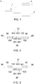
FIG. 1 , thesemi-transparent film 2 is configured between twoshading areas 1 in the conventional mask plate. When conducting the exposure process, the twoshading areas 1 are completely opaque, and thus thephotoresist 3 with respect to the twoshading areas 1 may be reserved. And only the part of the light may pass through thesemi-transparent film 2, thus thephotoresist 3 with respect to thesemi-transparent film 2 may be partially exposed. In the subsequent process, the remaining photoresist with respect to thesemi-transparent film 2 is completely ashed. And a channel of the TFT is obtained corresponding to thesemi-transparent film 2 after a series of processes. - The manufacturing process of the TFT adopting the conventional mask plate may require longer time for conducting the exposure process and the ashing process, which may result in lower productivity and greater power-consuming.
- The present disclosure relates to a mask plate and a manufacturing method of an array substrate configured to reduce the time for conducting the exposure process and the ashing process, so as to reduce power-consuming.
- In one aspect, the present disclosure relate to the mask plate including:
- a first area configured with at least two first sub-areas, wherein the first sub-areas are spaced apart from each other, and the first sub-areas are configured to be semi-transparent areas;
- a second area configured with at least one second sub-area, wherein the second sub-area is configured between the first sub-areas, and a transmittance rate of the second sub-area is greater than the first sub-area;
- a third area and a fourth area respectively configured next to two sides of the first area;
- a fifth area and a sixth area respectively configured next to one side of the third area and one side of the fourth area, wherein the side of the third area and the side of the fourth area are facing away the first area; wherein the second sub-area is configured to be a hollow area or to be a non-hollow area having the transmittance rate greater than the first sub-area;
- a first area configured with at least two first sub-areas, wherein the first sub-areas are spaced apart from each other, and the first sub-areas are configured to be semi-transparent areas;
- a second area configured with at least one second sub-area, wherein the second sub-area is configured between the first sub-areas, and a transmittance rate of the second sub-area is greater than the first sub-area;
- In another aspect, the present disclosure relates to an array substrate, including:
- providing a substrate; forming a gate layer, an insulation layer covering the gate layer and the substrate, a semiconductor layer covering the insulation layer, a second metal layer covering the semiconductor layer, and a photoresist layer covering the second metal layer on the substrate in sequence;
- providing a mask plate and conducting an exposure process on the photoresist layer via the mask plate;
- conducting a development process and transferring patterns on the mask plate onto the photoresist layer;
- wherein the mask layer includes:
- a first area is configured with at least two first sub-areas, wherein the first sub-areas are spaced apart from each other, and the first sub-areas are configured to be semi-transparent areas;
- a second area is configured with at least one second sub-area, wherein the second sub-area is configured between the first sub-areas, and a transmittance rate of the second sub-area is greater than the first sub-area; when conducting an exposure process on a photoresist, a thickness of the exposed photoresist via the second sub-area is greater than a thickness of the exposed photoresist via the first sub-area, and the photoresist layer with respect to the first sub-area and the second sub-area is partially exposed.
- In view of the above, the first area in the mask plate of the present disclosure is configured to be the semi-transparent area and is configured with the at least two first sub-area spaced apart from each other. When manufacturing the array substrate, due to the transmittance rate of the second sub-area is greater than the first sub-area, the thickness of the exposed photoresist on the second sub-area is greater than the thickness of the exposed photoresist on the first sub-area. The photoresist corresponding to the second sub-area may be exposed deeper under the same exposure amount when being compared with the conventional exposure process. As such, the present disclosure may reduce the time and the power for the exposure process. In the subsequent ashing process, the present disclosure may terminate the ashing process upon the photoresist corresponding to the second sub-area is completely ashed, and the thickness of the exposed photoresist corresponding to the second sub-area is less than the exposed photoresist corresponding to the first sub-area. After conducting the development process, the thickness of the remaining photoresist corresponding to the second sub-area is less than the thickness of the remaining photoresist corresponding to the first sub-area. As such, the time and the power for conducting the ashing process may be reduced, and the productivity may be improved.
-
-
FIG. 1 is a schematic view of a conventional mask plate when conducting an exposure process. -
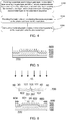
FIG. 2 is a schematic view of a mask plate in one embodiment of the present disclosure. -
FIG. 3 is a schematic view of a mask plate in one embodiment of the present disclosure. -
FIG. 4 is a flowchart of a manufacturing method of array substrates in one embodiment of the present disclosure. -
FIG. 5 is a schematic view illustrating an array substrate in step S100 shown inFIG. 4 in one embodiment of the present disclosure. -
FIG. 6 is a schematic view illustrating an array substrate in step S200 shown inFIG. 4 in one embodiment of the present disclosure. -
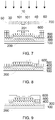
FIG. 7 is a schematic view illustrating the array substrate in step S200 shown inFIG. 4 in another embodiment of the present disclosure. -
FIG. 8 is a schematic view illustrating an array substrate in step S300 shown inFIG. 4 in one embodiment of the present disclosure. -
FIG. 9 is a schematic view illustrating an array substrate in step S400 in one embodiment of the present disclosure. -
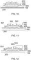
FIG. 10 is a schematic view illustrating an array substrate in step S500 in one embodiment of the present disclosure. -
FIG. 11 is a schematic view illustrating an array substrate in step S600 in one embodiment of the present disclosure. -
FIG. 12 is a schematic view illustrating the array substrate in step S600 in another embodiment of the present disclosure. - Referring to
FIG. 2 , the present disclosure relates to a mask plate, including: afirst area 10, asecond area 20, athird area 30, afourth area 40, afifth area 50, and asixth area 60. - The
first area 10 is configured with at least twofirst sub-areas 101, wherein thefirst sub-areas 101 are spaced apart from each other, and at least onegap 102 are configured between thefirst sub-areas 101. In one example, as shown inFIG. 2 , thefirst area 10 may include threefirst sub-areas 101, but is not limited. In another example, the first area may include two, three, or even more first sub-areas. - The
first sub-areas 101 are configured to be semi-transparent areas, and thus only a portion of the light beams may pass through thefirst sub-areas 101, the remaining portions of the light beams may be reflected. Specifically, thefirst sub-areas 101 may be made of semi-transparent film. - The
second area 20 is configured with at least onesecond sub-area 201, wherein thesecond sub-area 201 is configured in thegap 102 between thefirst sub-areas 101. In one example, as shown inFIG. 2 , thefirst area 10 may include threefirst sub-areas 101, and thesecond area 20 may include twosecond sub-areas 201. - A transmittance rate of the
second sub-area 201 is greater than thefirst sub-area 101. As such, when conducting an exposure process on a photoresist via the mask plate during the manufacturing process of the substrate, a thickness of the exposed photoresist via thesecond sub-area 201 is greater than a thickness of the exposed photoresist via thefirst sub-areas 101. A thickness of the remaining photoresist of thesecond sub-area 201 is less than a thickness of the remaining photoresist of thefirst sub-areas 101 after a development process. An ashing process is conducted on the remaining photoresist, and the ashing process may be terminated upon the photoresist corresponding to the second sub-area is completely ashed. And at least one channel may be formed on the array substrate corresponding to the at least onesecond sub-area 201 after conducting an etching process. - Conventionally, the photoresist corresponding to a whole
semi-transparent film 2 is exposed to the same degree. However, the present disclosure may only expose the at least one second sub-area to a required thickness. Due to the transmittance rate of the at least onesecond sub-area 201 is greater than the at least twofirst sub-area 101, the exposure time and the power may be reduced in the present disclosure when being compared with the conventional manufacturing method. The ashing process may only be conducted on the remaining photoresist corresponding to thesecond sub-area 201 in the present disclosure, such that the time and time power for the ashing process may be reduced, so as to improve to productivity. - In one example, the
second sub-area 201 is configured to be a hollow area or to be a non-hollow area having the transmittance rate greater than thefirst sub-area 101. Thesecond sub-area 201 is configured to be the hollow area that indicates thefirst area 10 used to be a complete semi-transparent area, such as a complete transparent film, and at least one sub-area of thefirst area 10 is hollowed out to form the at least twofirst sub-area 101 spaced apart from each other. The hollowed portion of thefirst sub-area 101 is configured to be the at least onesecond sub-area 201. A width of thesecond sub-area 201 is less than a resolution of an exposure machine, for example less than 2.5mm, of an exposure machine so as to guarantee the channel may be formed on the array substrate corresponding to the second sub-area, so that a diffraction effect may occur and the subsequent process may be completed. - In one example, in order to obtain a thinner channel of the array substrate, the exposed photoresist via the
second sub-area 201 corresponds to thesecond sub-area 201 when conducting the exposure process on the photoresist. As such, the channel of the array substrate may correspond to thesecond sub-area 201 after a series manufacturing process, wherein the width of the channel is configured to be the width of the photoresist. Conventionally, the width of the channel is configured to be a width of a gap between twoshading areas 1. The present disclosure adopts the mask plate to reduce the width of the channel and to improve charging rate. Specifically, thesecond area 20 may include one or twosecond sub-areas 201. When thesecond area 20 includes two second sub-areas 201, a double seam interference effect may be occurred, such that a bright strip may be formed within an area corresponding to the photoresist after the light beams pass through the twosecond sub-areas 201. The exposure process may be conducted via the bright stripe. As such, the exposure position of the two second sub-areas 201 may be the same. The channel may be formed after the series manufacturing process. - In one example, the mask plate may include the
third area 30, thefourth area 40, thefifth area 50, and thesixth area 60. - The
third area 30 and thefourth area 40 are respectively configured next to two sides of thefirst area 10. Thethird area 30 and thefourth area 40 may be in the same plane with thefirst area 10, as shown inFIG. 2 , and may not be in the same plane with thefirst area 10, as shown inFIG. 3 . Wherein thethird area 30 and thefourth area 40 are configured to be theshading areas 40. In one example, as shown inFIG. 3 , thefirst area 10 may be configured below thethird area 30 and thefourth area 40. In another example, thefirst area 10 may be configured on thethird area 30 and thefourth area 40. - The
fifth area 50 and thesixth area 60 are respectively configured next to one side of thethird area 30 and one side of thefourth area 40, wherein the side of thethird area 30 and the side of thefourth area 40 are facing away thefirst area 10, and thefifth area 50 and thesixth area 60 are configured to be full translucent areas. - Referring to
FIG. 4 , the present disclosure further relates to a manufacturing process of the array substrates, including the following steps. - In S100: providing a substrate and forming a gate layer, an insulation layer covering the gate layer and the substrate, a semiconductor layer covering the insulation layer, a second metal layer covering the semiconductor layer, and a photoresist layer covering the second metal layer on the substrate in sequence.
- Referring to
FIG. 5 , thesubstrate 100 is provided. Thesubstrate 100 is made of a material having good optical performance, high transparency, and low reflectivity. In one example, thesubstrate 100 may be made of glass. - The
gate layer 200, theinsulation layer 300 covering thegate layer 200 and thesubstrate 100, thesemiconductor layer 400 covering theinsulation layer 300, thesecond metal layer 500 covering thesemiconductor layer 400, and thephotoresist layer 600 covering thesecond metal layer 500 are formed on thesubstrate 100 in sequence. - Specifically, the step of forming the
gate layer 200 further includes: forming a first metal layer (not shown) on thesubstrate 100, and conducting a patterned process on the first metal layer to form thegate layer 200. - The
gate layer 200 and thesecond metal layer 500 are made of one or more combination of molybdenum, titanium, aluminum and copper. Theinsulation layer 300 is made of one or more combination of silicon oxide and silicon nitride. Thesemiconductor layer 400 is made of amorphous silicon or polysilicon. - In S200: providing the mask plate and conducting the exposure process on the photoresist layer via the mask plate.
- Referring to
FIG. 6 , themask plate 700 is provided, and the exposure process is conducted on thephotoresist layer 600 via themask plate 700, wherein themask plate 700 may be configured to be one of the mask plates described above, and may not be described again. - The exposure process is to transfer patters of the
mask plate 700 onto thephotoresist 600 by exposing the ultraviolet (UV). A s shown inFIG. 6 , after conducting the exposure process, thephotoresist layer 600 may be divided into afirst exposure area 601 and asecond exposure area 602, wherein thefirst exposure area 601 corresponds to the at least twofirst sub-areas 101 of themask plate 700, and thesecond exposure area 602 corresponds to the at least onesecond sub-area 201. - The transmittance rate of the
second sub-area 201 is greater than thefirst sub-area 101, and thus when conducting the exposure process on the photoresist, a thickness of the exposedsecond exposure area 602 is greater than a thickness of the exposed first exposure area. Due to thefirst sub-area 101 is configured to be the semi-transparent area, the transmittance rate of a non-hollowed area of thesecond sub-area 201 is greater than thefirst sub-area 101, and the width of the hollowed area of thesecond sub-area 201 is less than the resolution of the exposure machine, the photoresist of thephotoresist layer 600 corresponding to thefirst sub-area 101 and thesecond sub-area 102 is partially exposed when conducting the exposure process. - In view of the above, the present disclosure may only expose the photoresist corresponding to the at least two
second sub-area 201 to the required thickness, and the photoresist corresponding to thesecond sub-area 201 may be exposed deeper under the same exposure amount when being compared with the conventional exposure process. As such, the present disclosure may reduce the time and the power for the exposure process and may improve the productivity. - In one example, the
mask plate 700 may include thethird area 30, thefourth area 40, thefifth area 50, and thesixth area 60. After conducting the exposure process, the photoresist layer may further include athird exposure area 603 and afourth exposure area 604. Wherein thethird exposure area 603 corresponds to thethird area 30 andfourth area 40 of themask plate 700 and thefourth area 604 corresponds to thefifth area 50 and thesixth area 60 of themask plate 700. Thethird area 30 and thefourth area 40 are configured to be the shading areas, and thus the photoresist corresponding to thethird exposure area 603 is partially exposed. Thefifth area 50 and thesixth area 60 are configured to be the full-transparent areas, and thus thephotoresist layer 600 corresponding to thefourth exposure area 604 is completely exposed. - In order to obtain the thinner channel, the exposed
photoresist layer 600 via thesecond sub-area 201 of themask plate 700 corresponds to thesecond sub-area 201 when conducting the exposure process on thephotoresist layer 600 via themask plate 700. In one example, as shown inFIG. 7 , thesecond area 20 may include one or twosecond sub-area 201. When thesecond area 20 includes two second sub-areas 201, the double seam interference effect may be conducted, such that the bright strip may be formed within the area corresponding to the photoresist. The exposure process may be conducted on the photoresist layer via the bright stripe. - In S300: conducting the development process and transferring patterns on the mask plate onto the photoresist layer.
- As shown in
FIG. 8 , the development process is conducted via developer. Specifically, the exposed photoresist may be dissolved, and the patterns of themask plate 700 may be transferred onto thephotoresist layer 600. - In one example, after the step S300, the manufacturing method may further include the following steps.
- In S400: conducting the patterned process on the second metal layer and the semiconductor layer via the remaining photoresist of the photoresist layer.
- As shown in
FIG. 9 , a first etching process is conducted to remove a first portion of thesecond metal layer 500 and thesemiconductor layer 400, wherein the portion of thesecond metal layer 500 and thesemiconductor layer 400 are not covered by thephotoresist layer 600. - In one example, after the step S400, the manufacturing method may further include the following steps.
- In S500: conducting the ashing process on the remaining photoresist of the photoresist layer and terminating the ashing process upon the photoresist layer corresponding to the second sub-area is completely ashed.
- As shown in
FIG. 10 , the ashing process is conducted on the remainingphotoresist layer 600, and the ashing process may be terminated upon the photoresist of the photoresist layer corresponding to the second sub-area is completely ashed. - The thickness of the remaining photoresist corresponding to the
second sub-area 201 is less than the thickness of the remaining photoresist corresponding to thefirst sub-area 101. Conventionally, the ashing process is conducted on the whole of the remaining photoresist on thesemi-transparent film 2. Therefore, the present disclosure may reduce time and power for conducting the ashing process and may improve productivity when being compared with the conventional manufacturing method. - In one example, after the step S500, the manufacturing method may further include the following steps.
- In S600: conducting the patterned process on the second metal layer and the semiconductor layer via the remaining photoresist layer, wherein the at least one channel is formed on the array substrate corresponding to the at least one second sub-area.
- As shown in
FIG. 11 , a second etching process is conducted to remove a second portion of thesecond metal layer 500 and thesemiconductor layer 400, so as to form asource 501 and adrain 502, wherein the second portion of thesecond metal layer 500 and thesemiconductor layer 400 are not covered by thephotoresist layer 600. The at least onechannel 503 is formed on the array substrate corresponding to the at least onesecond sub-area 201. - As shown in
FIG. 12 , the exposed photoresist of thephotoresist layer 700 corresponding to thesecond sub-area 201 corresponds to thesecond sub-area 201 when conducting the exposure process on the photoresist, and the onechannel 503 may be obtained. Conventionally, the width of thechannel 503 is configured to be as a width of thewhole semiconductor film 2. The width of thechannel 503 in the present disclosure is configured to be as the width of the exposed photoresist. As such, the present disclosure may reduce the width of the channel and may improve charging rate when being compared with the conventional manufacturing method. In addition, the drain and the source may be formed on the array substrate corresponding to thefirst area 10, so as to reduce the size of the TFT and to improve opening rate. - In view of the above, the first area in the mask plate of the present disclosure is configured to be the semi-transparent area and is configured with the at least two first sub-area spaced apart from each other. When manufacturing the array substrate, due to the transmittance rate of the second sub-area is greater than the first sub-area, the thickness of the exposed photoresist on the second sub-area is greater than the thickness of the exposed photoresist on the first sub-area. The photoresist corresponding to the second sub-area may be exposed deeper under the same exposure amount when being compared with the conventional exposure process. As such, the present disclosure may reduce the time and power for the exposure process. In the subsequent ashing process, the present disclosure may terminate the ashing process upon the photoresist corresponding to the second sub-area is completely ashed, and the thickness of the exposed photoresist corresponding to the second sub-area is less than the exposed photoresist corresponding to the first sub-area. After conducting the development process, the thickness of the remaining photoresist corresponding to the second sub-area is less than the thickness of the remaining photoresist corresponding to the first sub-area. As such, the time and the power for conducting the ashing process may be reduced, and the productivity may be improved.
- The above description is merely the embodiments in the present disclosure, the claim is not limited to the description thereby. The equivalent structure or changing of the process of the content of the description and the figures, or to implement to other technical field directly or indirectly should be included in the claim.
Claims (12)
- A mask plate, comprising:a first area configured with at least two first sub-areas, wherein the first sub-areas are spaced apart from each other, and the first sub-areas are configured to be semi-transparent areas;a second area configured with at least one second sub-area, wherein the second sub-area is configured between the first sub-areas, and a transmittance rate of the second sub-area is greater than the first sub-area;a third area and a fourth area respectively configured next to two sides of the first area;a fifth area and a sixth area respectively configured next to one side of the third area and one side of the fourth area, wherein the side of the third area and the side of the fourth area are facing away the first area;wherein the second sub-area is configured to be a hollow area or to be a non-hollow area having the transmittance rate greater than the first sub-area;when the second sub-area is configured to be the hollow area, a width of the second sub-area is less than a resolution of an exposure machine, the third area and the fourth area are configured to be shading areas, and the fifth area and the sixth area are configured to be full translucent areas;when conducting an exposure process on a photoresist, a thickness of the exposed photoresist via the second sub-area is greater than a thickness of the exposed photoresist via the first sub-area;when manufacturing an array substrate, a channel of the array substrate corresponds to the second sub-area.
- The mask plate according to claim 1, wherein the exposed photoresist via the second sub-area corresponds to the second sub-area when conducting the exposure process on the photoresist.
- A mask plate, comprising:a first area configured with at least two first sub-areas, wherein the first sub-areas are spaced apart from each other, and the first sub-areas are configured to be semi-transparent areas;a second area configured with at least one second sub-area, wherein the second sub-area is configured between the first sub-areas, and a transmittance rate of the second sub-area is greater than the first sub-area;wherein a thickness of the exposed photoresist via the second sub-area is greater than a thickness of the exposed photoresist via the first sub-area when conducting an exposure process on a photoresist;when manufacturing an array substrate, at least one channel of the array substrate corresponds to the at least one second sub-area.
- The mask plate according to claim 3, wherein the second sub-area is configured to be a hollow area or to be a non-hollow area having the transmittance rate greater than the first sub-area, when the second sub-area is configured to be the hollow area, a width of the second sub-area is less than a resolution of an exposure machine.
- The mask plate according to claim 4, wherein the exposed photoresist via the second sub-area corresponds to the second sub-area when conducting the exposure process on the photoresist.
- The mask plate according to claim 3, wherein the mask plate further comprises:a third area and a fourth area are respectively configured next to two sides of the first area;a fifth area and a sixth area are respectively configured next to one side of the third area and one side of the fourth area, wherein the side of the third area and the side of the fourth area are facing away the first area;wherein the third area and the fourth area are configured to be shading areas, and the fifth area and the sixth area are configured to be full translucent areas.
- A manufacturing method of an array substrate, comprising:providing a substrate;forming a gate layer, an insulation layer covering the gate layer and the substrate, a semiconductor layer covering the insulation layer, a second metal layer covering the semiconductor layer, and a photoresist layer covering the second metal layer on the substrate in sequence;providing a mask plate and conducting an exposure process on the photoresist layer via the mask plate;conducting a development process and transferring patterns on the mask plate onto the photoresist layer;wherein the mask layer comprises:a first area is configured with at least two first sub-areas, wherein the first sub-areas are spaced apart from each other, and the first sub-areas are configured to be semi-transparent areas;a second area is configured with at least one second sub-area, wherein the second sub-area is configured between the first sub-areas, and a transmittance rate of the second sub-area is greater than the first sub-area;when conducting an exposure process on a photoresist, a thickness of the exposed photoresist via the second sub-area is greater than a thickness of the exposed photoresist via the first sub-area, and the photoresist layer with respect to the first sub-area and the second sub-area is partially exposed.
- The manufacturing method according to claim 7, wherein the step of providing the mask plate and conducting the exposure process on the photoresist layer via the mask plate further comprises:the second sub-area is configured to be a hollow area or to be a non-hollow area having the transmittance rate greater than the first sub-area;when the second sub-area is configured to be the hollow area, a width of the second sub-area is less than a resolution of an exposure machine.
- The manufacturing method according to claim 8, wherein the step of providing the mask plate and conducting the exposure process on the photoresist layer via the mask plate further comprises:
the exposed photoresist via the second sub-area corresponds to the second sub-area when conducting the exposure process on the photoresist. - The manufacturing method according to claim 7, wherein the mask plate further comprises:a third area and a fourth area are respectively configured next to two sides of the first area;a fifth area and a sixth area are respectively configured next to one side of the third area and one side of the fourth area, wherein the side of the third area and the side of the fourth area are facing away the first area;the third area and the fourth area are configured to be shading areas, and the fifth area and the sixth area are configured to be full translucent areas.
- The manufacturing method according to claim 10, wherein the manufacturing method further comprises:conducting a patterned process in the second metal layer and the semiconductor layer via the remaining photoresist of the photoresist layer;conducting an ashing process on the remaining photoresist of the photoresist layer;terminating the ashing process upon the photoresist layer corresponding to the second sub-area is completely ashed.
- The manufacturing method according to claim 11, wherein the manufacturing method further comprises:conducting the patterned process on the second metal layer and the semiconductor layer via the remaining photoresist layer;wherein at least one channel is formed on the array substrate corresponding to the at least one second sub-area.
Applications Claiming Priority (2)
| Application Number | Priority Date | Filing Date | Title |
|---|---|---|---|
| CN201710325080.1A CN107132724B (en) | 2017-05-10 | 2017-05-10 | A kind of preparation method of mask plate and array substrate |
| PCT/CN2017/088614 WO2018205345A1 (en) | 2017-05-10 | 2017-06-16 | Mask and method for preparing array substrate |
Publications (2)
| Publication Number | Publication Date |
|---|---|
| EP3640976A1 true EP3640976A1 (en) | 2020-04-22 |
| EP3640976A4 EP3640976A4 (en) | 2021-03-03 |
Family
ID=59732781
Family Applications (1)
| Application Number | Title | Priority Date | Filing Date |
|---|---|---|---|
| EP17908931.3A Withdrawn EP3640976A4 (en) | 2017-05-10 | 2017-06-16 | MASK AND METHOD FOR PREPARING NETWORK SUBSTRATE |
Country Status (6)
| Country | Link |
|---|---|
| US (1) | US10345697B2 (en) |
| EP (1) | EP3640976A4 (en) |
| JP (1) | JP6895525B2 (en) |
| KR (1) | KR102316173B1 (en) |
| CN (1) | CN107132724B (en) |
| WO (1) | WO2018205345A1 (en) |
Cited By (1)
| Publication number | Priority date | Publication date | Assignee | Title |
|---|---|---|---|---|
| US12317593B2 (en) | 2020-02-26 | 2025-05-27 | Fuzhou Boe Optoelectronics Technology Co., Ltd. | Array substrate and display panel having array substrate |
Families Citing this family (3)
| Publication number | Priority date | Publication date | Assignee | Title |
|---|---|---|---|---|
| CN109136834B (en) * | 2018-09-07 | 2021-03-05 | 京东方科技集团股份有限公司 | Mask, OLED display substrate and preparation method thereof |
| CN109343304B (en) | 2018-11-21 | 2020-04-14 | 惠科股份有限公司 | A method for making a photomask and a display panel for making an active switch |
| CN115064635B (en) * | 2022-06-07 | 2025-05-30 | 广州华星光电技术有限公司 | Method for manufacturing side wiring of substrate and display panel |
Family Cites Families (23)
| Publication number | Priority date | Publication date | Assignee | Title |
|---|---|---|---|---|
| US7241539B2 (en) * | 2002-10-07 | 2007-07-10 | Samsung Electronics Co., Ltd. | Photomasks including shadowing elements therein and related methods and systems |
| JP4009219B2 (en) * | 2003-04-10 | 2007-11-14 | 松下電器産業株式会社 | Photomask, pattern formation method using the photomask, and mask data creation method |
| KR100616708B1 (en) * | 2004-04-12 | 2006-08-28 | 엘지.필립스 엘시디 주식회사 | LCD array substrate and manufacturing method thereof |
| KR101190045B1 (en) * | 2005-12-21 | 2012-10-12 | 엘지디스플레이 주식회사 | The photo mask and method of fabricating the array substrate for liquid crystal display device using the same |
| KR101255616B1 (en) * | 2006-07-28 | 2013-04-16 | 삼성디스플레이 주식회사 | Multi-tone optical mask, method of manufacturing the same and method of manufacturing thin film transistor substrate using the same |
| CN101211118A (en) * | 2006-12-25 | 2008-07-02 | 上海广电Nec液晶显示器有限公司 | LCD device preparation method and mask used in the method |
| JP2009063638A (en) * | 2007-09-04 | 2009-03-26 | Fujitsu Microelectronics Ltd | Photomask manufacturing method and semiconductor device manufacturing method |
| KR101407306B1 (en) * | 2007-12-31 | 2014-06-16 | 엘지디스플레이 주식회사 | Mask and method for manufacturing thin film transistor substrate using same |
| CN101546733B (en) * | 2008-03-28 | 2011-07-27 | 北京京东方光电科技有限公司 | Method for manufacturing TFT-LCD array substrate and color film substrate |
| TWI373097B (en) * | 2008-07-09 | 2012-09-21 | Au Optronics Corp | Method for fabricating thin film transistor array substrate |
| KR101237096B1 (en) * | 2008-08-21 | 2013-02-25 | 엘지디스플레이 주식회사 | Method for manufacturing thin film transistor array substrate |
| JP5595004B2 (en) * | 2008-10-21 | 2014-09-24 | 株式会社半導体エネルギー研究所 | Display device |
| CN101738846B (en) * | 2008-11-17 | 2012-02-29 | 北京京东方光电科技有限公司 | Mask plate and preparation method thereof |
| KR101079161B1 (en) * | 2008-12-22 | 2011-11-02 | 엘지이노텍 주식회사 | Half tone mask and fabricating method |
| TWI444758B (en) * | 2009-06-19 | 2014-07-11 | 友達光電股份有限公司 | Thin film transistor element and photomask and thin film transistor element for defining thin film transistor element |
| CN101615594A (en) * | 2009-08-14 | 2009-12-30 | 上海广电光电子有限公司 | The manufacture method of thin-film transistor array base-plate |
| JP5123349B2 (en) * | 2010-04-19 | 2013-01-23 | Hoya株式会社 | Multi-tone mask manufacturing method |
| JP5917020B2 (en) * | 2010-06-29 | 2016-05-11 | Hoya株式会社 | Manufacturing method of mask blank and multi-tone mask |
| TWI424507B (en) * | 2011-04-15 | 2014-01-21 | 中華映管股份有限公司 | Method for manufacturing thin film transistor array substrate |
| KR101425064B1 (en) * | 2011-06-09 | 2014-08-01 | 엘지디스플레이 주식회사 | Oxide thin film transistor and method of fabricating the same |
| CN102707575B (en) * | 2012-05-18 | 2015-02-25 | 北京京东方光电科技有限公司 | Mask plate and method for manufacturing array substrate |
| CN103165471A (en) * | 2013-02-19 | 2013-06-19 | 京东方科技集团股份有限公司 | Thin film transistor and manufacture method and display device thereof |
| KR20170035408A (en) * | 2015-09-22 | 2017-03-31 | 삼성디스플레이 주식회사 | Thin film transistor array panel and manufacturing method thereof |
-
2017
- 2017-05-10 CN CN201710325080.1A patent/CN107132724B/en active Active
- 2017-06-16 EP EP17908931.3A patent/EP3640976A4/en not_active Withdrawn
- 2017-06-16 KR KR1020197035836A patent/KR102316173B1/en active Active
- 2017-06-16 JP JP2019538607A patent/JP6895525B2/en active Active
- 2017-06-16 US US15/541,681 patent/US10345697B2/en active Active
- 2017-06-16 WO PCT/CN2017/088614 patent/WO2018205345A1/en not_active Ceased
Cited By (1)
| Publication number | Priority date | Publication date | Assignee | Title |
|---|---|---|---|---|
| US12317593B2 (en) | 2020-02-26 | 2025-05-27 | Fuzhou Boe Optoelectronics Technology Co., Ltd. | Array substrate and display panel having array substrate |
Also Published As
| Publication number | Publication date |
|---|---|
| CN107132724A (en) | 2017-09-05 |
| KR20200003180A (en) | 2020-01-08 |
| KR102316173B1 (en) | 2021-10-26 |
| CN107132724B (en) | 2019-11-26 |
| JP6895525B2 (en) | 2021-06-30 |
| US20180329287A1 (en) | 2018-11-15 |
| JP2020505639A (en) | 2020-02-20 |
| WO2018205345A1 (en) | 2018-11-15 |
| US10345697B2 (en) | 2019-07-09 |
| EP3640976A4 (en) | 2021-03-03 |
Similar Documents
| Publication | Publication Date | Title |
|---|---|---|
| TWI674662B (en) | Manufacturing method of array substrate | |
| US9698171B2 (en) | Array substrate and method of manufacturing the same, and display device | |
| US8134158B2 (en) | TFT-LCD pixel unit and method for manufacturing the same | |
| US6479398B1 (en) | Method of manufacturing an amorphous-silicon thin film transistor | |
| KR101255616B1 (en) | Multi-tone optical mask, method of manufacturing the same and method of manufacturing thin film transistor substrate using the same | |
| CN106206456B (en) | Manufacturing method of array substrate, array substrate and display device | |
| CN103165529B (en) | Preparation method of array baseplate | |
| EP2530720B1 (en) | Manufacture methods of thin film transistor and array substrate and mask | |
| CN105742240B (en) | A kind of manufacturing method of LTPS array substrate | |
| WO2020073474A1 (en) | Method for manufacturing tft array substrate | |
| US10345697B2 (en) | Mask plates and manufacturing methods of array substrates | |
| CN103346159B (en) | A kind of array base palte and manufacture method, display device | |
| US6391499B1 (en) | Light exposure mask and method of manufacturing the same | |
| TWI578546B (en) | Method for manufacturing thin film transistor | |
| CN105185743B (en) | The preparation method of thin-film transistor array base-plate | |
| CN103035652A (en) | Array substrate of fringe filed switching type liquid-crystal display panel and production method of array substrate | |
| TWI424507B (en) | Method for manufacturing thin film transistor array substrate | |
| JP2004014622A (en) | Method of manufacturing thin film semiconductor device and method of forming resist pattern thereof | |
| WO2020073547A1 (en) | Thin film transistor and manufacturing method therefor | |
| TWI396916B (en) | Thin film transistor array substrate manufacturing method | |
| CN110047738B (en) | Mask, thin film transistor, array substrate, manufacturing method and display device | |
| KR101577234B1 (en) | Method for Forming Patterns and Method for Manufacturing Thin Film Transistor Substrate | |
| JP3071964B2 (en) | Manufacturing method of liquid crystal display device | |
| CN102830531B (en) | TFT (Thin Film Transistor) array substrate, manufacturing method and liquid crystal display device | |
| TWI766198B (en) | Display panel and method of manufacturing the same |
Legal Events
| Date | Code | Title | Description |
|---|---|---|---|
| STAA | Information on the status of an ep patent application or granted ep patent |
Free format text: STATUS: THE INTERNATIONAL PUBLICATION HAS BEEN MADE |
|
| PUAI | Public reference made under article 153(3) epc to a published international application that has entered the european phase |
Free format text: ORIGINAL CODE: 0009012 |
|
| STAA | Information on the status of an ep patent application or granted ep patent |
Free format text: STATUS: REQUEST FOR EXAMINATION WAS MADE |
|
| 17P | Request for examination filed |
Effective date: 20191128 |
|
| AK | Designated contracting states |
Kind code of ref document: A1 Designated state(s): AL AT BE BG CH CY CZ DE DK EE ES FI FR GB GR HR HU IE IS IT LI LT LU LV MC MK MT NL NO PL PT RO RS SE SI SK SM TR |
|
| AX | Request for extension of the european patent |
Extension state: BA ME |
|
| DAV | Request for validation of the european patent (deleted) | ||
| DAX | Request for extension of the european patent (deleted) | ||
| A4 | Supplementary search report drawn up and despatched |
Effective date: 20210129 |
|
| RIC1 | Information provided on ipc code assigned before grant |
Ipc: G03F 1/54 20120101ALI20210125BHEP Ipc: G03F 1/50 20120101ALI20210125BHEP Ipc: H01L 21/77 20170101AFI20210125BHEP Ipc: H01L 27/12 20060101ALI20210125BHEP |
|
| STAA | Information on the status of an ep patent application or granted ep patent |
Free format text: STATUS: EXAMINATION IS IN PROGRESS |
|
| 17Q | First examination report despatched |
Effective date: 20230605 |
|
| GRAP | Despatch of communication of intention to grant a patent |
Free format text: ORIGINAL CODE: EPIDOSNIGR1 |
|
| STAA | Information on the status of an ep patent application or granted ep patent |
Free format text: STATUS: GRANT OF PATENT IS INTENDED |
|
| INTG | Intention to grant announced |
Effective date: 20231023 |
|
| STAA | Information on the status of an ep patent application or granted ep patent |
Free format text: STATUS: THE APPLICATION IS DEEMED TO BE WITHDRAWN |
|
| 18D | Application deemed to be withdrawn |
Effective date: 20240305 |