EP3638639B1 - Verfahren zur herstellung eines schaltungsträgers - Google Patents
Verfahren zur herstellung eines schaltungsträgers Download PDFInfo
- Publication number
- EP3638639B1 EP3638639B1 EP18731088.3A EP18731088A EP3638639B1 EP 3638639 B1 EP3638639 B1 EP 3638639B1 EP 18731088 A EP18731088 A EP 18731088A EP 3638639 B1 EP3638639 B1 EP 3638639B1
- Authority
- EP
- European Patent Office
- Prior art keywords
- carrier substrate
- ceramic material
- vol
- laser
- carrier
- Prior art date
- Legal status (The legal status is an assumption and is not a legal conclusion. Google has not performed a legal analysis and makes no representation as to the accuracy of the status listed.)
- Active
Links
Images




Classifications
-
- C—CHEMISTRY; METALLURGY
- C04—CEMENTS; CONCRETE; ARTIFICIAL STONE; CERAMICS; REFRACTORIES
- C04B—LIME, MAGNESIA; SLAG; CEMENTS; COMPOSITIONS THEREOF, e.g. MORTARS, CONCRETE OR LIKE BUILDING MATERIALS; ARTIFICIAL STONE; CERAMICS; REFRACTORIES; TREATMENT OF NATURAL STONE
- C04B35/00—Shaped ceramic products characterised by their composition; Ceramics compositions; Processing powders of inorganic compounds preparatory to the manufacturing of ceramic products
- C04B35/01—Shaped ceramic products characterised by their composition; Ceramics compositions; Processing powders of inorganic compounds preparatory to the manufacturing of ceramic products based on oxide ceramics
- C04B35/10—Shaped ceramic products characterised by their composition; Ceramics compositions; Processing powders of inorganic compounds preparatory to the manufacturing of ceramic products based on oxide ceramics based on aluminium oxide
- C04B35/111—Fine ceramics
- C04B35/117—Composites
-
- C—CHEMISTRY; METALLURGY
- C04—CEMENTS; CONCRETE; ARTIFICIAL STONE; CERAMICS; REFRACTORIES
- C04B—LIME, MAGNESIA; SLAG; CEMENTS; COMPOSITIONS THEREOF, e.g. MORTARS, CONCRETE OR LIKE BUILDING MATERIALS; ARTIFICIAL STONE; CERAMICS; REFRACTORIES; TREATMENT OF NATURAL STONE
- C04B35/00—Shaped ceramic products characterised by their composition; Ceramics compositions; Processing powders of inorganic compounds preparatory to the manufacturing of ceramic products
- C04B35/622—Forming processes; Processing powders of inorganic compounds preparatory to the manufacturing of ceramic products
- C04B35/626—Preparing or treating the powders individually or as batches ; preparing or treating macroscopic reinforcing agents for ceramic products, e.g. fibres; mechanical aspects section B
- C04B35/63—Preparing or treating the powders individually or as batches ; preparing or treating macroscopic reinforcing agents for ceramic products, e.g. fibres; mechanical aspects section B using additives specially adapted for forming the products, e.g.. binder binders
- C04B35/632—Organic additives
- C04B35/636—Polysaccharides or derivatives thereof
-
- C—CHEMISTRY; METALLURGY
- C04—CEMENTS; CONCRETE; ARTIFICIAL STONE; CERAMICS; REFRACTORIES
- C04B—LIME, MAGNESIA; SLAG; CEMENTS; COMPOSITIONS THEREOF, e.g. MORTARS, CONCRETE OR LIKE BUILDING MATERIALS; ARTIFICIAL STONE; CERAMICS; REFRACTORIES; TREATMENT OF NATURAL STONE
- C04B41/00—After-treatment of mortars, concrete, artificial stone or ceramics; Treatment of natural stone
- C04B41/009—After-treatment of mortars, concrete, artificial stone or ceramics; Treatment of natural stone characterised by the material treated
-
- C—CHEMISTRY; METALLURGY
- C04—CEMENTS; CONCRETE; ARTIFICIAL STONE; CERAMICS; REFRACTORIES
- C04B—LIME, MAGNESIA; SLAG; CEMENTS; COMPOSITIONS THEREOF, e.g. MORTARS, CONCRETE OR LIKE BUILDING MATERIALS; ARTIFICIAL STONE; CERAMICS; REFRACTORIES; TREATMENT OF NATURAL STONE
- C04B41/00—After-treatment of mortars, concrete, artificial stone or ceramics; Treatment of natural stone
- C04B41/45—Coating or impregnating, e.g. injection in masonry, partial coating of green or fired ceramics, organic coating compositions for adhering together two concrete elements
- C04B41/50—Coating or impregnating, e.g. injection in masonry, partial coating of green or fired ceramics, organic coating compositions for adhering together two concrete elements with inorganic materials
- C04B41/51—Metallising, e.g. infiltration of sintered ceramic preforms with molten metal
-
- C—CHEMISTRY; METALLURGY
- C04—CEMENTS; CONCRETE; ARTIFICIAL STONE; CERAMICS; REFRACTORIES
- C04B—LIME, MAGNESIA; SLAG; CEMENTS; COMPOSITIONS THEREOF, e.g. MORTARS, CONCRETE OR LIKE BUILDING MATERIALS; ARTIFICIAL STONE; CERAMICS; REFRACTORIES; TREATMENT OF NATURAL STONE
- C04B41/00—After-treatment of mortars, concrete, artificial stone or ceramics; Treatment of natural stone
- C04B41/80—After-treatment of mortars, concrete, artificial stone or ceramics; Treatment of natural stone of only ceramics
- C04B41/81—Coating or impregnation
- C04B41/85—Coating or impregnation with inorganic materials
- C04B41/88—Metals
-
- H—ELECTRICITY
- H05—ELECTRIC TECHNIQUES NOT OTHERWISE PROVIDED FOR
- H05K—PRINTED CIRCUITS; CASINGS OR CONSTRUCTIONAL DETAILS OF ELECTRIC APPARATUS; MANUFACTURE OF ASSEMBLAGES OF ELECTRICAL COMPONENTS
- H05K1/00—Printed circuits
- H05K1/02—Details
- H05K1/03—Use of materials for the substrate
- H05K1/0306—Inorganic insulating substrates, e.g. ceramic, glass
-
- H—ELECTRICITY
- H05—ELECTRIC TECHNIQUES NOT OTHERWISE PROVIDED FOR
- H05K—PRINTED CIRCUITS; CASINGS OR CONSTRUCTIONAL DETAILS OF ELECTRIC APPARATUS; MANUFACTURE OF ASSEMBLAGES OF ELECTRICAL COMPONENTS
- H05K3/00—Apparatus or processes for manufacturing printed circuits
- H05K3/10—Apparatus or processes for manufacturing printed circuits in which conductive material is applied to the insulating support in such a manner as to form the desired conductive pattern
- H05K3/18—Apparatus or processes for manufacturing printed circuits in which conductive material is applied to the insulating support in such a manner as to form the desired conductive pattern using precipitation techniques to apply the conductive material
- H05K3/181—Apparatus or processes for manufacturing printed circuits in which conductive material is applied to the insulating support in such a manner as to form the desired conductive pattern using precipitation techniques to apply the conductive material by electroless plating
- H05K3/182—Apparatus or processes for manufacturing printed circuits in which conductive material is applied to the insulating support in such a manner as to form the desired conductive pattern using precipitation techniques to apply the conductive material by electroless plating characterised by the patterning method
- H05K3/185—Apparatus or processes for manufacturing printed circuits in which conductive material is applied to the insulating support in such a manner as to form the desired conductive pattern using precipitation techniques to apply the conductive material by electroless plating characterised by the patterning method by making a catalytic pattern by photo-imaging
-
- C—CHEMISTRY; METALLURGY
- C04—CEMENTS; CONCRETE; ARTIFICIAL STONE; CERAMICS; REFRACTORIES
- C04B—LIME, MAGNESIA; SLAG; CEMENTS; COMPOSITIONS THEREOF, e.g. MORTARS, CONCRETE OR LIKE BUILDING MATERIALS; ARTIFICIAL STONE; CERAMICS; REFRACTORIES; TREATMENT OF NATURAL STONE
- C04B2111/00—Mortars, concrete or artificial stone or mixtures to prepare them, characterised by specific function, property or use
- C04B2111/00474—Uses not provided for elsewhere in C04B2111/00
- C04B2111/00844—Uses not provided for elsewhere in C04B2111/00 for electronic applications
-
- C—CHEMISTRY; METALLURGY
- C04—CEMENTS; CONCRETE; ARTIFICIAL STONE; CERAMICS; REFRACTORIES
- C04B—LIME, MAGNESIA; SLAG; CEMENTS; COMPOSITIONS THEREOF, e.g. MORTARS, CONCRETE OR LIKE BUILDING MATERIALS; ARTIFICIAL STONE; CERAMICS; REFRACTORIES; TREATMENT OF NATURAL STONE
- C04B2235/00—Aspects relating to ceramic starting mixtures or sintered ceramic products
- C04B2235/02—Composition of constituents of the starting material or of secondary phases of the final product
- C04B2235/30—Constituents and secondary phases not being of a fibrous nature
- C04B2235/32—Metal oxides, mixed metal oxides, or oxide-forming salts thereof, e.g. carbonates, nitrates, (oxy)hydroxides, chlorides
- C04B2235/3281—Copper oxides, cuprates or oxide-forming salts thereof, e.g. CuO or Cu2O
-
- C—CHEMISTRY; METALLURGY
- C04—CEMENTS; CONCRETE; ARTIFICIAL STONE; CERAMICS; REFRACTORIES
- C04B—LIME, MAGNESIA; SLAG; CEMENTS; COMPOSITIONS THEREOF, e.g. MORTARS, CONCRETE OR LIKE BUILDING MATERIALS; ARTIFICIAL STONE; CERAMICS; REFRACTORIES; TREATMENT OF NATURAL STONE
- C04B2235/00—Aspects relating to ceramic starting mixtures or sintered ceramic products
- C04B2235/02—Composition of constituents of the starting material or of secondary phases of the final product
- C04B2235/50—Constituents or additives of the starting mixture chosen for their shape or used because of their shape or their physical appearance
- C04B2235/54—Particle size related information
- C04B2235/5409—Particle size related information expressed by specific surface values
-
- C—CHEMISTRY; METALLURGY
- C04—CEMENTS; CONCRETE; ARTIFICIAL STONE; CERAMICS; REFRACTORIES
- C04B—LIME, MAGNESIA; SLAG; CEMENTS; COMPOSITIONS THEREOF, e.g. MORTARS, CONCRETE OR LIKE BUILDING MATERIALS; ARTIFICIAL STONE; CERAMICS; REFRACTORIES; TREATMENT OF NATURAL STONE
- C04B2235/00—Aspects relating to ceramic starting mixtures or sintered ceramic products
- C04B2235/02—Composition of constituents of the starting material or of secondary phases of the final product
- C04B2235/50—Constituents or additives of the starting mixture chosen for their shape or used because of their shape or their physical appearance
- C04B2235/54—Particle size related information
- C04B2235/5418—Particle size related information expressed by the size of the particles or aggregates thereof
- C04B2235/5445—Particle size related information expressed by the size of the particles or aggregates thereof submicron sized, i.e. from 0,1 to 1 micron
-
- C—CHEMISTRY; METALLURGY
- C04—CEMENTS; CONCRETE; ARTIFICIAL STONE; CERAMICS; REFRACTORIES
- C04B—LIME, MAGNESIA; SLAG; CEMENTS; COMPOSITIONS THEREOF, e.g. MORTARS, CONCRETE OR LIKE BUILDING MATERIALS; ARTIFICIAL STONE; CERAMICS; REFRACTORIES; TREATMENT OF NATURAL STONE
- C04B2235/00—Aspects relating to ceramic starting mixtures or sintered ceramic products
- C04B2235/65—Aspects relating to heat treatments of ceramic bodies such as green ceramics or pre-sintered ceramics, e.g. burning, sintering or melting processes
- C04B2235/656—Aspects relating to heat treatments of ceramic bodies such as green ceramics or pre-sintered ceramics, e.g. burning, sintering or melting processes characterised by specific heating conditions during heat treatment
- C04B2235/6567—Treatment time
-
- H—ELECTRICITY
- H05—ELECTRIC TECHNIQUES NOT OTHERWISE PROVIDED FOR
- H05K—PRINTED CIRCUITS; CASINGS OR CONSTRUCTIONAL DETAILS OF ELECTRIC APPARATUS; MANUFACTURE OF ASSEMBLAGES OF ELECTRICAL COMPONENTS
- H05K2203/00—Indexing scheme relating to apparatus or processes for manufacturing printed circuits covered by H05K3/00
- H05K2203/10—Using electric, magnetic and electromagnetic fields; Using laser light
- H05K2203/107—Using laser light
Definitions
- the invention relates to a method for producing a circuit carrier with a carrier substrate. Furthermore, the invention relates to a carrier substrate for a ceramic material, a use of a ceramic material as a carrier substrate, and the ceramic material as such.
- Thermoplastics containing additives provided with metal compounds are usually used to produce circuit carriers and in particular injection-molded circuit carriers.
- the circuit carriers are usually manufactured using the so-called laser direct structuring (LDS method).
- LDS method laser direct structuring
- a laser beam writes a desired layout directly onto the surface of a corresponding plastic-based carrier substrate.
- the surface of the plastic is decomposed into volatile cleavage products and slightly removed.
- metal nuclei are split off from the additive and are finely distributed in the micro-rough surface. These metal nuclei serve as a catalyst for the subsequent metallization.
- a conductor profile or a conductor structure with sharp contours is created in a currentless copper bath on the lasered partial areas of the surface. Layers of copper, nickel and finally gold (Cu/Ni/Au coating) can be applied one after the other.
- circuit carriers due to the limited thermal stability of such plastic-based circuit carriers, the area of application is restricted. Especially in areas where circuit carriers are exposed to high loads, such as in medical technology, in aviation and aerospace, in the automotive industry or when they are used in LED-based lighting fixtures, circuit carriers are required that are characterized by good chemical, thermal and mechanical stability and a low thermal expansion coefficient.
- Circuit carriers made of ceramic materials represent an alternative that is suitable for such purposes.
- the screen printing process or LTCC (Low Temperature Cofired Ceramics) and HTCC (High Temperature Cofired Ceramics) techniques are often used.
- LTCC Low Temperature Cofired Ceramics
- HTCC High Temperature Cofired Ceramics
- a ceramic substrate which is used as a carrier substrate for a circuit carrier.
- the ceramic substrate is made of an inorganic powder and an organic molding resin.
- the inorganic powder comprises 72-98% by weight aluminum oxide, 1-12% by weight copper oxide, 0.1-3% by weight titanium oxide and 0.25-10% by weight silicon oxide.
- a conductive paste is applied to a green body of the ceramic material and fired together with the green body.
- the invention is therefore based on the object of specifying a possibility that allows improved and simplified production of circuit carriers that can be used in a variety of ways.
- a carrier substrate is provided, in the surface of which a structure for a conductor to be applied is introduced by means of a laser.
- the structure is provided with a metallic coating forming the conductor, forming the circuit carrier.
- a ceramic material with a composition comprising 85 to 99% by volume of aluminum oxide (Al 2 O 3 ) and 1 to 15% by volume of copper oxide (Cu 2 O) is used as the carrier substrate.
- the method according to the invention enables ceramic-based three-dimensional circuit carriers to be generated by means of additive manufacturing processes.
- the method of laser structuring which has hitherto been unsuitable (or only partially) suitable for ceramic materials, can be used for the simple and effective production of three-dimensional circuit carriers.
- electrically conductive conductor structures i.e. structures with the appropriately applied conductors
- the carrier substrate i.e. on the Al 2 O 3 ceramic substrate material doped with Cu 2 O, which new chemical compounds with contain special properties.
- the ceramic material is first selectively activated using the laser-based structuring technique.
- the structure introduced into the surface of the carrier substrate by means of laser processing is then coated with metal to form the circuit carrier.
- composition of the ceramic material used within the scope of the method according to the invention for producing the circuit carrier increases the laser activity, the precision when introducing the structures and the quality of the metallization. Since the copper contained in the composition serves as a catalyst for the copper deposition, the copper layer thickness of the circuit carrier produced by means of the method according to the invention is increased after metallization in comparison to conventional laser structuring of ceramic materials.
- Laser structurability and metallization of the carrier substrate are further improved if a ceramic material is used as the carrier substrate with a composition that preferably contains 94 to 98% by volume of aluminum oxide (Al 2 O 3 ) and 2 to 6% by volume of copper oxide ( Cu 2 O).
- Al 2 O 3 aluminum oxide
- Cu 2 O copper oxide
- the sum of the components included in the composition of the ceramic material ie the sum of the proportions of aluminum oxide (Al 2 O 3 ) and copper oxide (Cu 2 O), is 100% by volume.
- this 100% by volume also includes the usual (particularly minor) impurities, for example depending on the purity of the starting materials used and/or the respective process used to produce the ceramic material.
- the ceramic material can contain residues of an organic binder or other additives (eg a dispersing agent) as process-related impurities.
- the carrier substrate is advantageously produced by sintering at temperatures between 1000.degree. C. and 1800.degree. It is particularly advantageous within the scope of the invention if the carrier substrate is produced by sintering at temperatures between 1100° C. and 1300° C.
- lasers with a specific wavelength of the emitted light and a very low power are required.
- the laser wavelength for structuring the surface of the laser substrate is preferably 1064 nm.
- a laser type: Nd:YAg is expediently used for this purpose.
- a structure for a conductor to be applied is understood to mean in principle any structure or any surface profile introduced into the surface of a carrier substrate for the production of a corresponding circuit carrier. This includes in particular both linear and planar structures. However, the structures are of course not limited to these designs, but are in particular adapted to the requirements of the circuit carrier or matched to its intended area of use.
- the structures are preferably introduced into the surface of the carrier substrate with a laser power in a range between 4 watts and 12 watts.
- the preferred laser speed is in a range between 0.75 m/s to 2.25 m/s.
- the laser pulse frequency with which the structures are introduced into the surface of the carrier substrate is preferably in a range between 60 kHz and 120 kHz.
- the use of a ceramic material as the carrier substrate with a composition comprising 95% by volume Al 2 O 3 and 5% by volume Cu 2 O is particularly preferred.
- the surface is preferably laser structured with a laser power of 4 watts, a laser speed of 1.5 m/s and a laser frequency of 120 kHz.
- the structure introduced into the surface of the carrier substrate or the respective profile is expediently provided with a metallic coating containing Cu-Ni-Au.
- the coating is preferably carried out by a chemical electroless metallization method.
- copper, nickel and gold are applied one after the other in an electroless manner to the surface structure of the carrier substrate, forming the circuit carrier.
- standard layer thicknesses are achieved.
- the quality and durability of the metallization are excellent, especially with regard to surface roughness, adhesion of the metallization and durability.
- the copper conductor tracks produced in this way have a diameter of 160 ⁇ m.
- the smallest distance between two conductor tracks is 20 ⁇ m.
- the layer thickness is in the range of 8.2 ⁇ m to 12.2 ⁇ m.
- the roughness of the surface after laser exposure is in the range between 21 ⁇ m and 36 ⁇ m.
- the first step in electroless metallization is cleaning by means of ultrasound in deionized water. Cleaning takes place at a temperature of 293 K and an exposure time of at least 5 minutes. It is then rinsed with deionized water.
- the respective component i.e. the carrier substrate, is completely immersed in a copper plating solution.
- the copper plating solution consists of 15% by volume to 40% by volume of copper(II) sulfate CuSO 4 and formaldehyde COH 2 and is adjusted to a pH value of: 11-13 with sodium hydroxide solution NaOH.
- the bathroom has a temperature in a range between 318K and 333K.
- dry, de-oiled atmospheric air is blown into the bath from the bottom of the bath at room temperature with a volume flow of 1 l/min and a pressure of 1200 hPa.
- the copper layers are built up at a rate of 2 ⁇ m/h to 5 ⁇ m/h.
- the component is thoroughly cleaned in several stages in deionized water at a temperature of 293K.
- the component is then immersed in an aqueous, highly acidic palladium sulfate solution for 30 s to 60 seconds and then rinsed.
- the component treated in this way is immersed in an acidic nickel(I) phosphate solution for the nickel plating.
- the nickel is deposited at a rate of 4 ⁇ m/h to 6 ⁇ m/h nickel at a bath temperature between 348 K and 363 K.
- the gold layer is applied with approx.
- Ceramic substrates in printed circuit board technology are often used in power electronics. This requires copper layers of up to 200 ⁇ m so that high currents can be transported.
- galvanic metallization is particularly preferred.
- the structures, which have already been generated without current, are contacted with a clamp (cathode) and immersed in a sulfuric acid CuSO 4 solution. There is a Cu anode in the solution. If a DC voltage is now applied between the two electrodes, Cu(2+) ions are continuously deposited on the structures according to Faraday's law. With this method, predefined Cu layer thicknesses can be generated.
- the carrier substrate according to the invention for a circuit carrier comprises a ceramic material with a composition comprising 85 to 99% by volume aluminum oxide (Al 2 O 3 ) and 1 to 15% by volume copper oxide (Cu 2 O).
- the carrier substrate particularly preferably comprises a ceramic material with a composition comprising 94 to 98% by volume of aluminum oxide (Al 2 O 3 ) and 2 to 6% by volume of copper oxide (Cu 2 O).
- the carrier substrate is preferably produced by sintering at temperatures between 1000°C and 1800°C. It is particularly advantageous if the carrier substrate is produced by sintering at temperatures between 1100°C and 1300°C.
- a ceramic material with a composition comprising 85 to 99% by volume of aluminum oxide (Al 2 O 3 ) and 1 to 15% by volume of copper oxide (Cu 2 O) is used as a carrier substrate for a circuit carrier, the carrier substrate in particular is used in the above-described inventive method for producing a circuit carrier.
- the use of a ceramic material with a composition comprising 94 to 98% by volume aluminum oxide (Al 2 O 3 ) and 2 to 6% by volume copper oxide (Cu 2 O) as a carrier substrate for a circuit carrier is particularly preferred.
- a mixture of aluminum oxide and copper oxide according to the invention ie a composition of Al 2 O 3 doped with Cu 2 O, as a ceramic material for a carrier substrate results in a new material after thermal treatment of the corresponding mixture, ie after sintering.
- CuAlO 2 and CuAl 2 O 4 are formed as reaction products, with the concentration of CuAl 2 O 4 increasing as the sintering temperature rises.
- the phases take on a certain order in the new material, which influences the properties of the material.
- a further processing of a Workpiece with the composition according to the invention is especially well suited for direct laser structuring.
- the ceramic material used as a carrier substrate for a circuit carrier is preferably produced by sintering at temperatures between 1000°C and 1800°C.
- the ceramic material used as the carrier substrate for a circuit carrier is particularly preferably produced by sintering at temperatures between 1100.degree. C. and 1300.degree.
- the ceramic material according to the invention for a carrier substrate of a circuit carrier has a composition which comprises 85 to 99% by volume aluminum oxide (Al 2 O 3 ) and 1 to 15% by volume copper oxide (Cu 2 O). More preferably, the ceramic material for a circuit carrier has a composition that includes 94 to 98% by volume of aluminum oxide (Al 2 O 3 ) and 2 to 6% by volume of copper oxide (Cu 2 O). The sum of all components included in the composition of the ceramic material - including the usual minor impurities - is 100% by volume.
- the ceramic material is produced by sintering at temperatures between 1000°C and 1800°C. Ceramic material is also preferably produced by sintering at temperatures between 1100°C and 1300°C.
- FIG. 1 shows the particle size distribution of the particle mixture used to produce a carrier substrate according to the invention (i.e. the Educts Al 2 O 3 , Cu 2 O and dextrin) in a plot 1 of the particle diameter [ ⁇ m] versus the relative volume fraction [%] of the educts in the mixture.
- the three starting materials Al 2 O 3 , Cu 2 O and dextrin were dispersed in deionized water by adding a Darvan CN dispersant solution (Electrosteric dispersant, ammonium salt of polymethacrylic acid, rt Vanderbilt Co. Inc. Norwalk, CT, USA).
- a Darvan CN dispersant solution Electrodeic dispersant, ammonium salt of polymethacrylic acid, rt Vanderbilt Co. Inc. Norwalk, CT, USA.
- Table 1 lists the specific properties of the starting materials used to produce a ceramic material.
- the binder-supported aqueous Al 2 O 3 -Cu 2 O suspension was homogenized in a tumble mixer ( Turbula® , Willy A. Bachofen AG, Switzerland) with Al 2 O 3 grinding balls over a period of 24 h and then freeze-dried at a pressure of 0.38 mPa (Delta 2-24, Christ, Osterode/Harz, Germany). Since no shrinkage can be observed during freeze-drying due to the lack of capillary forces, the mechanical strength and porosity of the obtained freeze-dried blanks (batches) are dependent on the content of the solvent (water) in the resulting ceramic slurry.
- the dried batches were ground for a further 24 hours and sieved through a sieve with a mesh size of 150 ⁇ m.
- the aluminum oxide (Al 2 O 3 ) and the copper oxide (Cu 2 O) particles are homogeneously distributed after sludging, freeze drying and grinding and have a dextrin layer, so that the further shaping process can also be used to produce ceramic Green compacts can be used with relatively high mechanical strength.
- the volume ratios of Al 2 O 3 and Cu 2 O varies.
- the ground and sieved powders were mixed in different volume ratios and then uniaxially pressed at a pressure of 200 MPa into a cylindrical shape with a diameter of 40 mm and a thickness of 2 mm to 5 mm (Paul Weber, Maschinen und Apparatebau, Stuttgart, Germany). Subsequently, the binder-supported Cu 2 O-Al 2 O 3 molded parts were sintered in air at temperatures of 1200° C., 1400° C. and 1600° C. for 1 hour.
- microstructures (determined by EDX analysis) of two samples with different Cu 2 O-Al 2 O 3 - concentrations in the powder mixtures used after sintering at different temperatures are in the Figures 2 to 5 shown.
- 2 and 3 are microscopic images 9, 11 of a ceramic material 12 produced by sintering at 1200° C. with a ratio of Al 2 O 3 to Cu 2 O of 95% by volume to 5% by volume with a resolution of 200 ⁇ m ( 2 ), as well as with a resolution of 20 ⁇ m ( 3 ) shown.
- the 4 and 5 each show microscopic images13, 15 of a ceramic material produced by sintering at 1600 °C with a ratio of Al 2 O 3 to Cu 2 O from 85% by volume to 15% by volume with a resolution of 200 ⁇ m ( 4 ), as well as with a resolution of 20 ⁇ m ( figure 5 ).
- samples sintered at a temperature of 1200 °C form three different phases: an Al 2 O 3 phase 17, a Cu 2 O phase 19 and a CuAlO 2 phase 21, which in-situ through the Reaction between Al 2 O 3 and Cu 2 O was formed.
- the porosity after sintering at 1200 °C is around ⁇ 45%.
- the ceramic material 16 which was sintered at 1600 °C, has a denser microstructure with a residual porosity of only ⁇ 3% ( 4 , micrograph 13).
- an Al 2 O 3 phase 23 and a CuAl 2 O 4 phase 25 were observed in samples sintered at a temperature of 1600° C., namely an Al 2 O 3 phase 23 and a CuAl 2 O 4 phase 25.
- a Cu 2 O phase is due to the complete reaction of Cu 2 O at higher temperatures is no longer present.
- the CuAl 2 O 4 phase 25 can be enriched in the sintered products.
- the results obtained from the EDX analyzes were further confirmed by XRD (X-ray diffraction) analyses.
- XRD X-ray diffraction
- Such an XRD analysis is in plot 26 is in 6 shown.
- the plot 26 shows a curve 27 for a sample with 85% by volume Al 2 O 3 and 15% by volume Cu 2 O, which was sintered at a temperature of 1200 ° C, and a curve 28 for a sample with 85 % by volume Al 2 O 3 and 15 % by volume Cu 2 O, which was sintered at a temperature of 1600°C.
- Cu +1 (eg in Cu 2 O and CuAlO 2 - in plot 26 indicated by circular symbols (Cu 2 O) and crosses (CuAlO 2 )) is still present, while Cu +1 after oxidized to Cu +2 during sintering at 1600°C (CuO and CuAl 2 O 4 - indicated in plot 26 by open squares (CuO) and asterisks (CuAl 2 O 4 )).
- Various structures were introduced into the surfaces of the manufactured substrates using a laser in order to check the suitability of the respective substrate (and thus the respective new material) for the manufacture of normal and micro-MID products.
- a series of measurements were carried out to check the effects of the structuring process on the substrate surface. Particular attention was paid to the ability to activate the surface and the properties of the structured area.
- the structuring was carried out with a laser power in a range between 4 watts and 12 watts, a laser speed in a range between 0.75 m/s to 2.25 m/s and a laser frequency in a range between 60 kHz and 120 kHz.
- the optimal parameters for laser structuring are a laser power of 4 watts, a laser speed of 1.5 m/s and a laser pulse frequency of 120 kHz.
- the ceramic materials according to the invention or the carrier substrates produced from them in contrast to standard polymer materials, which often have structuring defects, exhibit excellent properties both in grooved areas and in structured areas.
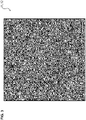
- 7 shows a representative 3D microscope laser scan 29 for a planar structured area 30 on the surface 31 of a carrier substrate 33 produced by sintering at 1200° C.
- the ratio of Al 2 O 3 to Cu 2 O is 95% by volume to 5 Vol%.
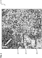
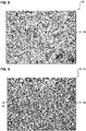
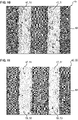
- FIG. 8 shows a section of a laser-structured carrier substrate 35 produced by sintering at 1200° C. with a planar structure 37 on the surface 39 of the carrier substrate 35.
- the ratio of Al 2 O 3 to Cu 2 O is also 95% by volume to 5 here Vol%.
- the same section of the laser-structured carrier substrate 35 is shown.
- the planar structure 37 of the carrier substrate 35 is already provided with a Cu/Ni/Au coating 41 forming the conductor 40 and can thus be used as a circuit carrier 43 .
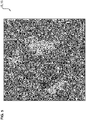
- FIG. 10 also shows a section of a laser-structured carrier substrate 45 sintered at 1200 °C.
- the ratio of Al 2 O 3 to Cu 2 O is 95% by volume to 5% by volume.
- the carrier substrate 45 has a linear structure 47 on the surface 49 of the carrier substrate 45 .
- Two adjacent ones can be seen Lanes 51. 11 the section of the laser-structured carrier substrate 45 according to 10 .
- the webs 51 (analogous to the planar structure 37 according to 9 ) is provided with a Cu/Ni/Au coating 53 forming the conductor 52, so that the carrier substrate 45 can also be used as a circuit carrier 55.
Landscapes
- Chemical & Material Sciences (AREA)
- Engineering & Computer Science (AREA)
- Ceramic Engineering (AREA)
- Structural Engineering (AREA)
- Organic Chemistry (AREA)
- Materials Engineering (AREA)
- Manufacturing & Machinery (AREA)
- Inorganic Chemistry (AREA)
- Microelectronics & Electronic Packaging (AREA)
- Composite Materials (AREA)
- Chemical Kinetics & Catalysis (AREA)
- Manufacturing Of Printed Wiring (AREA)
- Compositions Of Oxide Ceramics (AREA)
Description
- Die Erfindung betrifft ein Verfahren zur Herstellung eines Schaltungsträgers mit einem Trägersubstrat. Des Weiteren betrifft die Erfindung ein Trägersubstrat für einen keramischen Werkstoff, eine Verwendung eines keramischen Werkstoffes als Trägersubstrat, sowie den keramischen Werkstoff als solchen.
- Zur Herstellung von Schaltungsträgern und insbesondere von spritzgegossenen Schaltungsträgern werden üblicherweise thermoplastische Kunststoffe eingesetzt, die mit Metallverbindungen versehene Additive enthalten. Die Fertigung der Schaltungsträger erfolgt üblicherweise mittels der sogenannten Laser-Direkt- Strukturierung (LDS-Verfahren). Hierbei schreibt ein Laserstrahl ein gewünschtes Layout direkt auf die Oberfläche eines entsprechenden kunststoffbasierten Trägersubstrats. An den Stellen, an welchen der Laserstrahl auf den Kunststoff trifft, wird der Kunststoff oberflächlich in flüchtige Spaltprodukte zersetzt und geringfügig abgetragen. Gleichzeitig werden aus dem Additiv Metallkeime abgespalten, die feinst verteilt in der mikrorauen Oberfläche liegen. Diese Metallkeime dienen als Katalysator für die nachfolgende Metallisierung. In einem stromlosen Kupferbad entsteht ein Leiterprofil bzw. eine Leiterstruktur konturenscharf auf den gelaserten Teilbereichen der Oberfläche. Nacheinander lassen sich so Schichten aus Kupfer, Nickel und abschließend Gold (Cu/Ni/Au-Beschichtung) aufbringen.
- Aufgrund der begrenzten thermischen Stabilität solcher kunststoffbasierten Schaltungsträger ist den Einsatzbereich jedoch eingeschränkt. Insbesondere in Bereichen, in denen Schaltungsträger hohen Belastungen ausgesetzt sind, wie beispielsweise in der Medizintechnik, in der Luftfahrt- und Raumfahrt, in der Automobilindustrie oder bei deren Einsatz in LED-basierten Beleuchtungskörpern sind vielmehr Schaltungsträger notwendig, die sich durch gute chemische, thermische und mechanische Stabilität sowie durch einen geringen thermischen Ausdehnungskoeffizienten auszeichnen.
- Eine für solche Einsatzzwecke geeignete Alternative stellen Schaltungsträger aus keramischen Werkstoffen dar. Zu deren Herstellung werden häufig das Siebdruckverfahren oder LTCC (Low Temperature Cofired Ceramics) und HTCC (High Temperature Cofired Ceramics)-Techniken genutzt. Allerdings sind die keramischen Trägersubstrate bei diesen Verfahren hinsichtlich in ihrer Formgebung eingeschränkt.
- Weiter gab es Versuche, Keramiksubstrate aus reinem Aluminiumoxid (Al2O3) mittels eines additiven laserbasierten Prozesses zu strukturieren und anschließend zu metallisieren [AiF, Abschlussbericht IGF-Vorhaben 488ZN]. Die selektive Aktivierung der Oberfläche des Trägersubstrates erfolgte hierbei durch die Reduktion des Aluminium(III)-Oxides zu metallischen Aluminium mittels der in das Material eingekoppelten Laserenergie. Die so entstandenen Aluminiumatome wirkten katalytisch für die Kupferabscheidung bei der stromlosen Metallisierung. Allerdings ist die Reduktion des Aluminium(III)-Oxides aufgrund der geringen Elektronegativität schwierig. Gleichzeitig wird metallisches Aluminium durch Luftsauerstoff schnell oxidiert und verliert hierdurch seine katalytische Aktivität, was eine anschließende Metallisierung entsprechend erschwert.
- So ist beispielsweise aus
DE 694 07 499 T2 bekannt, ein gesintertes Aluminiumoxidteil oberflächlich mit einem UV-Lichtstrahl zu bestrahlen, der von einer gepulsten Excimerlaserquelle emittiert wird. Das bestrahlte Teil wird anschließend in eine autokatalytische Lösung eingetaucht, welche Ionen des Metalls enthält, welches gleichmäßig auf die bestrahlten Zonen des Teils niedergeschlagen werden soll. Das metallisierte Teil wird durch Löten oder Glühen in einer gesteuerten InertgasAtmosphäre erwärmt. - Aus
DE 10 2012 100 299 A1 ist ein Verfahren bekannt, bei dem auf einem Trägermaterial aufgebrachte Leiterbahnstrukturen durch einwirkende elektromagnetische Strahlung nicht selektiv aktiviert, sondern selektiv mit dem Trägermaterial verbunden werden. Hierzu wird eine Beschichtung auf das Trägermaterial aufgebracht, die anschließend selektiv mit der elektromagnetischen Strahlung bestrahlt wird. Die elektromagnetische Strahlung bewirkt hierbei, dass die in der Beschichtung enthaltenen Wirkstoffpartikel in die Oberfläche des Trägermaterials dispergiert werden. - Aus
US 2007/0142530 A1 ist ein Keramiksubstrat bekannt, das als Trägersubstrat für einen Schaltungsträger verwendet wird. Das Keramiksubstrat ist hergestellt aus einem inorganischen Pulver und einem organischen Gießharz. Das inorganische Pulver umfasst dabei 72-98 Gew.-% Aluminiumoxid, 1-12 Gew.-% Kupferoxid, 0,1-3 Gew.-% Titanoxid und 0,25-10 Gew.-% Siliziumoxid. Zur Herstellung von Leiterbahnen wird eine leitfähige Paste auf einen Grünkörper des Keramikmaterials aufgetragen und zusammen mit dem Grünkörper gebrannt. - Aus
GB 860,863 A - Ebenfalls bekannt sind laserstrukturierbare keramische Substrate, die Verbindungen von Cu-Cr-O enthalten. Die Herstellung solcher keramischen Substrate ist jedoch kostenintensiv und aufgrund des enthaltenen Chroms als umweltschädlich einzustufen.
- Der Erfindung liegt daher die Aufgabe zugrunde, eine Möglichkeit anzugeben, die eine verbesserte und vereinfachte Herstellung von vielfältig einsetzbaren Schaltungsträgern erlaubt.
- Diese Aufgabe wird erfindungsgemäß gelöst durch die Merkmale der Ansprüche 1, 8, 12 und 14. Vorteilhafte Ausgestaltungen der Erfindung sind in den Unteransprüchen und der nachfolgenden Beschreibung dargelegt.
- Im Rahmen des erfindungsgemäßen Verfahrens, welches zur Herstellung eines Schaltungsträgers angewandt wird, wird ein Trägersubstrat bereitgestellt, in dessen Oberfläche mittels eines Lasers eine Struktur für einen aufzubringenden Leiter eingebracht wird. Die Struktur wird unter Ausbildung des Schaltungsträgers mit einer den Leiter bildenden metallischen Beschichtung versehen. Als Trägersubstrat wird erfindungsgemäß ein keramischer Werkstoff mit einer Zusammensetzung, umfassend 85 bis 99 Vol.-% Aluminiumoxid (Al2O3), sowie 1 bis 15 Vol.-% Kupferoxid (Cu2O) eingesetzt.
- Dank des Einsatzes eines keramischen Werkstoffes mit der angegebenen Zusammensetzung als Trägersubstrat ermöglicht das erfindungsgemäße Verfahren die Generierung keramikbasierter dreidimensionaler Schaltungsträger mittels generativer Fertigungsprozesse. Mit anderen Worten lässt sich dank der erfindungsgemäßen Zusammensetzung des keramischen Werkstoffes das bislang für keramische Materialien nicht (oder lediglich bedingt) geeignete Verfahren der Laserstrukturierung zur einfachen und effektiven Herstellung von dreidimensionalen Schaltungsträgern einsetzen.
- Durch die Laserbearbeitung der Oberfläche des Trägersubstrates und den anschließenden Metallisierungsprozess lassen sich auf dem Trägersubstrat, also auf dem mit Cu2O dotierten Al2O3- Keramikträgermaterial elektrisch leitfähige Leiterstrukturen (also Strukturen mit den entsprechend aufgebrachten Leiter) herstellen, die neue chemische Verbindungen mit besonderen Eigenschaften enthalten. Mittels der laserbasierten Strukturierungstechnik wird der keramische Werkstoff zuerst selektiv aktiviert. Anschließend wird die mittels der Laserbearbeitung in die Oberfläche des Trägersubstrates eingebrachte Struktur unter Ausbildung des Schaltungsträgers metallisch beschichtet.
- Durch die im Rahmen des erfindungsgemäßen Verfahrens zur Herstellung des Schaltungsträgers eingesetzte Zusammensetzung des keramischen Werkstoffes werden die Laser-Aktivität, die Genauigkeit bei der Einbringung der Strukturen sowie die Metallisierungsqualität erhöht. Da das in der Zusammensetzung enthaltenen Kupfer als Katalysator für die Kupferabscheidung dient, ist die Kupferschichtdicke des mittels des erfindungsgemäßen Verfahrens hergestellten Schaltungsträgers nach der Metallisierung im Vergleich zur konventionellen Laserstrukturierung keramischer Materialien erhöht.
- Weiter verbessert werden die Laserstrukturierbarkeit und die Metallisierbarkeit des Trägersubstrates, wenn als Trägersubstrat ein keramischer Werkstoff mit einer Zusammensetzung eingesetzt wird, die vorzugsweise 94 bis 98 Vol.-% Aluminiumoxid (Al2O3), sowie 2 bis 6 Vol.-% Kupferoxid (Cu2O) umfasst.
- Insgesamt ergibt die Summe der von der Zusammensetzung des keramischen Werkstoffes umfassten Bestandteile, also die Summe der Anteile an Aluminiumoxid (Al2O3) und Kupferoxid (Cu2O), 100 Vol.-%. In diesen 100 Vol.-% sind selbstverständlich auch übliche (insbesondere geringfügige) Verunreinigungen, beispielsweise abhängig von Reinheit der eingesetzten Edukte und/oder dem jeweiligen zur Herstellung des keramischen Werkstoffes eingesetzten Verfahren mit berücksichtigt. Insbesondere kann der keramische Werkstoff im Rahmen der Erfindung Rückstände eines organischen Bindemittels oder weiterer Additive (z.B. eines Dispergiermittels) als verfahrensbedingte Verunreinigungen enthalten.
- Vorteilhafterweise wird das Trägersubstrat durch Sintern bei Temperaturen zwischen 1000°C und 1800°C hergestellt. Besonders von Vorteil ist es im Rahmen der Erfindung, wenn das Trägersubstrat durch Sintern bei Temperaturen zwischen 1100°C und 1300°C hergestellt wird.
- Grundlegend für das Verfahren zur Herstellung eines Schaltungsträgers mit einem Trägersubstrat aus einem keramischen Werkstoff mit einer Zusammensetzung, umfassend 85 bis 99 Vol.-% Aluminiumoxid (Al2O3), sowie 1 bis 15 Vol.-% Kupferoxid (Cu2O) und insbesondere 94 bis 98 Vol.-% Aluminiumoxid (Al2O3), sowie 2 bis 6 Vol.-% Kupferoxid (Cu2O) ist die gezielte Parameterauswahl zur Laserstrukturierung. Diese stellt aufgrund der Vielzahl möglicher Einstellungsparameter für den Strukturierungsprozess eine besondere Herausforderung dar.
- Zur Laserbehandlung eines Werkstückes und im Rahmen der Erfindung insbesondere zur gezielten Strukturierung der Oberfläche des Trägersubstrats (Einbringen von Strukturen als diskrete geometrische Strukturen) werden Laser mit einer speziellen Wellenlänge des emittierendes Lichtes und einer sehr geringen Leistung benötigt. Die Laserwellenlänge zur Strukturierung der Oberfläche des Lasersubstrates liegt vorzugsweise bei 1064nm. Hierzu wird zweckmäßigerweise ein Lasertyp: Nd:YAg eingesetzt.
- Unter einer Struktur für einen aufzubringenden Leiter wird im Rahmen der Erfindung grundsätzlich jede zur Herstellung eines entsprechenden Schaltungsträgers in die Oberfläche eines Trägersubstrates eingebrachte Struktur bzw. jedes Oberflächenprofil verstanden. Hiervon sind insbesondere sowohl linienförmige als auch flächige Strukturen umfasst. Selbstverständlich sind die Strukturen jedoch nicht auf diese Ausführungen beschränkt, sondern insbesondere an die Anforderungen des Schaltungsträgers angepasst bzw. auf dessen vorgesehenes Einsatzgebiet abgestimmt.
- Die Strukturen werden vorzugsweise mit einer Laserleistung in einem Bereich zwischen 4 Watt und 12 Watt in die Oberfläche des Trägersubstrates eingebracht. Die bevorzugte Lasergeschwindigkeit liegt in einem Bereich zwischen 0,75 m/s bis 2,25 m/s. Die Laserpulsfrequenz, mit welcher die Strukturen in die Oberfläche des Trägersubstrates eingebracht werden, liegt vorzugsweise in einem Bereich zwischen 60 kHz bis 120 kHz.
- Besonders bevorzugt ist der Einsatz eines keramischen Werkstoffes als Trägersubstrat mit einer Zusammensetzung, umfassend 95 Vol.-% Al2O3 und 5 Vol.-% Cu2O. Zur Herstellung eines Schaltungsträgers mit einem derart zusammengesetzten Trägersubstrat erfolgt die Laserstrukturierung der Oberfläche vorzugsweise mit einer Laserleistung von 4 Watt, einer Lasergeschwindigkeit von 1,5 m/s und einer Laserfrequenz von 120 kHz.
- Zweckmäßigerweise wird die in die Oberfläche des Trägersubstrates eingebrachte Struktur bzw. das jeweilige Profil mit einer Cu-Ni-Au enthaltenden metallische Beschichtung versehen. Die Beschichtung erfolgt vorzugsweise durch eine chemisch außenstromlose Metallisierungsmethode. Hierbei werden - unter Ausbildung des Schaltungsträgers - nacheinander Kupfer, Nickel und Gold stromlos auf die Oberflächenstruktur des Trägersubstrats aufgebracht. Bei der Beschichtung werden Standard-Schichtdicken erreicht. Die Qualität und die Beständigkeit der Metallisierung sind insbesondere im Hinblick auf die Oberflächenrauigkeit, die Haftung der Metallisierung und der Haltbarkeit hervorragend.
- Bei einem keramischen Werkstoff mit einer Zusammensetzung, umfassend 95 Vol.-% Al2O3 und 5 Vol.-% Cu2O, dessen Oberfläche wie vorstehend beschrieben strukturiert wurde (Laserleistung 4 Watt, Lasergeschwindigkeit 1,5 m/s und Laserfrequenz von 120 kHz) haben beispielsweise die so erzeugten Kupferleiterbahnen (also linienförmige Strukturen) einen Durchmesser von 160 µm. Der kleinste Abstand zwischen zwei Leiterbahnen liegt bei 20 µm. Die Schichtdicke liegt nach der Metallisierung im Bereich von 8,2 µm bis 12,2 µm. Die Rauheit der Oberfläche nach der Lasereinwirkung liegt im Bereich zwischen 21 µm und 36 µm.
- Die Metallisierung stellt sehr hohe Anforderungen an die hierzu eingesetzten Substanzen und den physikalischen Zustand der Lösungen. Im Folgenden ist in einer bevorzugten Ausgestaltung eine Variante einer stromlosen Metallisierung detailliert beschrieben. Der erste Schritt bei der stromlosen Metallisierung stellt die Reinigung mittels Ultraschall in vollentionisiertem Wasser dar. Die Reinigung erfolgt bei einer Temperatur von 293 K und einer Einwirkdauer von mindestens 5 min. Anschließend wird mit vollentionisiertem Wasser gespült. Zur selektiven Kupferabscheidung wird das jeweilige Bauteil, also das Trägersubstrat vollständig in eine Verkupferungslösung getaucht. Die Verkupferungslösung besteht zu je 15 Vol% bis 40 Vol% aus Kupfer(II)-Sulfat CuSO4 und Formaldehyd COH2 und wird mit Natronlauge NaOH auf einem pH-Wert von: 11 -13, eingestellt. Das Bad weist eine Temperatur in einem Bereich zwischen 318 K und 333K auf. Zur besseren Umspülung des entsprechenden Bauteils wird trockene, entölte Atmosphärenluft bei Raumtemperatur mit einem Volumenstrom von 1 l/min bei einem Druck von 1200 hPa ausgehend von der Unterseite des Bades in dieses eingeblasen. Der Schichtaufbau des Kupfers erfolgt mit einer Rate von 2 µm/h bis 5 µm/h.
- Nach der Kupferabscheidung erfolgt eine gründliche mehrstufige Reinigung des Bauteils in vollentionisiertem Wasser bei einer Temperatur von 293K. Anschließend wird das Bauteil für 30 s bis 60 Sekunden in eine wässrige, starksaure Palladiumsulfat-Lösung eingetaucht und anschließend gespült. Das auf diese Weise behandelte Bauteil wird für die Nickelabscheidung in eine saure Nickel(I)-Phosphatlösung getaucht. Die Nickelabscheidung erfolgt mit einer Rate von 4 µm/h bis 6 µm/h Nickel bei einer Badtemperatur zwischen 348 K und 363 K. Nach ca. 90 min wird das Bauteil aus dem Nickelbad entnommen und erneut mit vollentionisiertem Wasser gewaschen. Abschließend erfolgt die Aufbringung der Goldschicht mit ca. 0,04 µm Gold, einem sogenannten Goldflash, durch das Eintauchen des Bauteils in eine saure Goldcyanid-Lösung für einen Zeitraum von 5 min bis 15 min. Zum Schluss wird das Bauteil noch final mit vollentionisiertem Wasser gewaschen. Durch das Abscheiden der Metallionen an das Bauteil werden die jeweiligen Substanzen bzw. Stoffe aus den Lösungen entfernt und müssen während des Prozesses zudosiert werden.
- Keramische Substrate in der Leiterplattentechnik werden häufig in der Leistungselektronik eingesetzt. Hierzu sind Kupferschichten bis zu 200 µm notwendig, damit hohe Ströme transportiert werden können. Zur Verstärkung der Strukturen auf den neuartig strukturierten Schaltungsträgern ist insbesondere die galvanische Metallisierung bevorzugt. Dabei werden die bereits stromlos erzeugten Strukturen mit einer Klemme ankontaktiert (Kathode) und in eine schwefelsaure CuSO4-Lösung eingetaucht. In der Lösung befindet sich eine Cu-Anode. Wird nun eine Gleichspannung zwischen den beiden Elektroden angelegt scheiden sich an den Strukturen Cu (2+)-Ionen nach dem Faraday'schen Gesetz kontinuierlich ab. Mit dieser Methode können definiert vorgegebene Cu-Schichtdicken erzeugt werden.
- Das erfindungsgemäße Trägersubstrat für einen Schaltungsträger umfasst einen keramischen Werkstoff mit einer Zusammensetzung, umfassend 85 bis 99 Vol.-% Aluminiumoxid (Al2O3), sowie 1 bis 15 Vol.-% Kupferoxid (Cu2O). Besonders bevorzugt umfasst das Trägersubstrat einen keramischen Werkstoff mit einer Zusammensetzung umfassend 94 bis 98 Vol.-% Aluminiumoxid (Al2O3), sowie 2 bis 6 Vol.-% Kupferoxid (Cu2O).
- Das Trägersubstrat ist vorzugweise hergestellt durch Sintern bei Temperaturen zwischen 1000°C und 1800°C. Besonders von Vorteil es, wenn das Trägersubstrat durch Sintern bei Temperaturen zwischen 1100°C und 1300°C hergestellt ist.
- Weitere vorteilhafte Ausgestaltungen für das Trägersubstrat ergeben sich aus den auf das Verfahren gerichteten Unteransprüchen. Die hierzu benannten Vorteile können sinngemäß auf das Trägersubstrat übertragen werden.
- Erfindungsgemäß wird ein keramischer Werkstoff mit einer Zusammensetzung, umfassend 85 bis 99 Vol.-% Aluminiumoxid (Al2O3), sowie 1 bis 15 Vol.-% Kupferoxid (Cu2O) als Trägersubstrat für einen Schaltungsträger verwendet, wobei das Trägersubstrat insbesondere in dem vorstehend beschriebenen, erfindungsgemäßen Verfahren zur Herstellung eines Schaltungsträgers verwendet wird. Besonders bevorzugt ist die Verwendung eines keramischen Werkstoffes mit einer Zusammensetzung umfassend 94 bis 98 Vol.-% Aluminiumoxid (Al2O3), sowie 2 bis 6 Vol.-% Kupferoxid (Cu2O).als Trägersubstrat für einen Schaltungsträger.
- Durch die Verwendung einer erfindungsgemäßen Mischung aus Aluminiumoxid und Kupferoxid, also einer Zusammensetzung von mit Cu2O dotiertem Al2O3 als keramischer Werkstoff für ein Trägersubstrat entsteht nach einer thermischen Behandlung der entsprechenden Mischung, also nach dem Sintern ein neuer Werkstoff. Als Reaktionsprodukte entstehen CuAlO2 und CuAl2O4, wobei sich die Konzentration von CuAl2O4 mit steigender Sintertemperatur erhöht. Die Phasen nehmen in dem neuen Werkstoff eine bestimmte Ordnung an, durch welche die Eigenschaften des Materials beeinflusst werden. Eine Weiterverarbeitung eines Werkstückes mit der erfindungsgemäßen Zusammensetzung ist speziell für die Laserdirektstrukturierung besonders gut geeignet.
- Der als Trägersubstrat für einen Schaltungsträger eingesetzte keramische Werkstoff ist vorzugsweise durch Sintern bei Temperaturen zwischen 1000°C und 1800°C hergestellt. Besonders bevorzugt ist der als Trägersubstrat für einen Schaltungsträger verwendete keramische Werkstoff durch Sintern bei Temperaturen zwischen 1100°C und 1300°C hergestellt.
- Weitere vorteilhafte Ausgestaltungen für die Verwendung des keramischen Werkstoffes ergeben sich aus den auf das Verfahren und auf das Trägersubstrat gerichteten Unteransprüchen. Die hierzu benannten Vorteile können sinngemäß auf die Verwendung übertragen werden.
- Der erfindungsgemäße keramische Werkstoff für ein Trägersubstrat eines Schaltungsträgers weist eine Zusammensetzung auf, die 85 bis 99 Vol.-% Aluminiumoxid (Al2O3), sowie 1 bis 15 Vol.-% Kupferoxid (Cu2O) umfasst. Weiter bevorzugt weist der keramische Werkstoff für einen Schaltungsträger eine Zusammensetzung auf, die 94 bis 98 Vol.-% Aluminiumoxid (Al2O3), sowie 2 bis 6 Vol.-% Kupferoxid (Cu2O) umfasst. Die Summe aller von der Zusammensetzung des keramischen Werkstoffes umfassten Bestandteile - inklusive üblicher, geringfügiger Verunreinigungen - ergibt hierbei 100 Vol.-%.
- In vorteilhafter Ausgestaltung ist der keramische Werkstoff durch Sintern bei Temperaturen zwischen 1000°C und 1800°C hergestellt. Weiter bevorzugt ist keramischer Werkstoff hergestellt durch Sintern bei Temperatuten zwischen 1100°C und 1300°C.
- Weitere vorteilhafte Ausgestaltungen für die Verwendung des keramischen Werkstoffes ergeben sich aus den auf das Verfahren, auf das Trägersubstrat sowie auf die Verwendung gerichteten Unteransprüchen. Die hierzu benannten Vorteile können sinngemäß auf den keramischen Werkstoff übertragen werden.
- Nachfolgend werden Ausführungsbeispiele der Erfindung anhand einer Zeichnung näher erläutert. Darin zeigen:
- Fig. 1
- eine Auftragung einer Partikelgrößenverteilung der zur Herstellung eines keramischen Werkstoffes eingesetzten Edukte Al2O3, Cu2O und Dextrin,
- Fig. 2
- eine Mikroskopieaufnahme (SEM) eines durch Sintern bei 1200 °C hergestellten keramischen Werkstoffes mit einem Verhältnis von Al2O3 zu Cu2O von 95 Vol.-% zu 5 Vol.-%,
- Fig. 3
- die Mikroskopieaufnahme gemäß
Fig. 2 in 10-facher Vergrößerung, - Fig. 4
- eine weitere Mikroskopieaufnahme (SEM) eines durch Sintern bei 1600 °C hergestellten keramischen Werkstoffes mit einem Verhältnis von Al2O3:Cu2O von 85 Vol.-% zu 15 Vol.-%,
- Fig. 5
- die Mikroskopieaufnahme (SEM) gemäß
Fig. 4 in 10-facher Vergrößerung, - Fig. 6
- eine XRD-Aufnahme,
- Fig. 7
- einen 3D-Mikroskop-Laserscan für den strukturierten Bereich eines Trägersubstrates,
- Fig. 8
- einen Ausschnitt eines Trägersubstrats mit einer auf der Oberfläche eingebrachten flächigen Struktur,
- Fig. 9
- den Ausschnitt des Trägersubstrats gemäß
Fig. 8 mit der metallisierten flächigen Leiterstruktur, - Fig. 10
- einen Ausschnitt eines Trägersubstrats mit einer auf der Oberfläche eingebrachten linienförmigen Struktur, sowie
- Fig. 11
- den Ausschnitt des Trägersubstrats gemäß
Fig. 10 mit der metallisierten linienförmigen Leiterstruktur. - Einander entsprechende Teile und Größen sind in allen Figuren stets mit gleichen Bezugszeichen versehen.
-
Fig. 1 zeigt die Partikelgrößenverteilung der zur Herstellung eines erfindungsgemäßen Trägersubstrates eingesetzten Partikel-Mischung (also der eingesetzten Edukte Al2O3, Cu2O und Dextrin) in einer Auftragung 1 des Partikeldurchmessers [µm] gegen den relativen Volumenanteil [%] der Edukte in der Mischung. - Als Edukte wurden Submikron-Al2O3-Pulver (Kurve 3) (CT 3000 SG, Almatis GmbH, Ludwigshafen, Deutschland), Cu2O-Pulver (Kurve 5) (Strem Chemicals, Inc., KEHL, Deutschland) und Dextrin-Bindemittel (C6H10O5)n (Kurve 7) (Superior Gelbmittel F, Suedstaerke, Schrobenhausen, Deutschland, n = 10 - 200, d50 = 109 µm, Molekulargewicht 1600 - 32000 g/Mol) eingesetzt. Die drei Edukte Al2O3, Cu2O und Dextrin wurden in entionisiertem Wasser durch Zugabe einer Darvan C-N Dispergiermittel Lösung (Electrosteric Dispergiermittel Ammoniumsalz der Polymethacrylic Säure, r.t. Vanderbilt Co. Inc. Norwalk, CT, USA) dispergiert.
- In Tabelle 1 sind die die spezifischen Eigenschaften der zur Herstellung eines keramischen Werkstoffes eingesetzten Edukte aufgeführt.
Tabelle 1: Eigenschaften der eingesetzten Edukte Al2O3, Cu2O und Dextrin Al2O3 Dextrin Cu2O Spezifische Oberfläche [m2/g] 9.3 0.1 2,1 d 90 2.0 194.8 12.5 Partikelgröße [µm] d 50 0.8 109.0 5.5 d 10 0.3 50.8 1.7 - Die Bindemittel-gestützte wässrige Al2O3-Cu2O-Suspension wurde in einem Taumel-Mischer (Turbula®, Willy A. Bachofen AG, Schweiz) mit Al2O3-Schleifkugeln über einen Zeitraum von 24 h homogenisiert und anschließend bei einem Druck von 0,38 mPa gefriergetrocknet (Delta 2-24, Christ, Osterode/Harz, Deutschland). Da aufgrund des Fehlens von Kapillarkräften keine Schrumpfung während der Gefriertrocknung beobachtet werden kann, ist die mechanische Festigkeit und Porosität der erhaltenen gefriergetrockneten Rohlinge (Chargen) abhängig vom Gehalt des Lösungsmittels (Wasser) in dem resultierenden keramischen Schlamm.
- Nach der Gefriertrocknung wurden die getrockneten Chargen für weitere 24 Stunden gemahlen und durch ein Sieb mit einer Maschenweite von 150 µm gesiebt. Die Aluminiumoxid (Al2O3)- und die Kupferoxid (Cu2O)-Partikel sind nach der Verschlämmung, der Gefriertrocknung und dem Vermahlen homogen verteilt und weisen eine Dextrin-Schicht auf, so dass der weitere Formgebungsprozess auch zur Herstellung von Keramik-Grünlingen mit relativ hoher mechanischer Festigkeit genutzt werden kann.
- Da die Cu2O-Konzentration in der zur Herstellung des keramischen Werkstoffes eingesetzten Mischung eine wichtige Rolle für die endgültigen Materialeigenschaften, wie insbesondere die Laser-Aktivierbarkeit und die Dichte des keramischen Werkstoffes nach der thermischen Behandlung spielt, wurden die Volumenverhältnisse von Al2O3 und Cu2O variiert.
- Hierzu wurden die gemahlenen und gesiebten Pulver in verschiedene Volumenverhältnissen vermischt und anschließend einachsig bei einem Druck von 200 MPa in eine zylindrische Form mit einem Durchmesser von 40 mm und einer Dicke von 2 mm bis 5 mm gepresst (Paul Weber, Maschinen Und Apparatebau, Stuttgart, Deutschland). Anschließend wurden die Bindemittel-gestützten Cu2O-Al2O3-Formteile in Luft bei Temperaturen von 1200 °C, 1400 °C und 1600 °C für 1 Stunde gesintert.
- Die Mikrostrukturen (ermittelt durch EDX-Analyse) von zwei Proben mit unterschiedlichen Cu2O-Al2O3- Konzentrationen in den eingesetzten Pulver- Mischungen nach dem Sintern bei unterschiedlichen Temperaturen sind in den
Fig. 2 bis 5 gezeigt. In denFig. 2 und3 sind Mikroskopieaufnahmen 9, 11 eines durch Sintern bei 1200 °C hergestellten keramischen Werkstoffes 12 mit einem Verhältnis von Al2O3 zu Cu2O von 95 Vol.-% zu 5 Vol.-% mit einer Auflösung von 200 µm (Fig. 2 ), sowie mit einer Auflösung von 20 µm (Fig. 3 ) gezeigt. - Die
Fig. 4 und5 zeigen jeweils Mikroskopieaufnahmen13, 15 eines durch Sintern bei 1600 °C hergestellten keramischen Werkstoffes mit einem Verhältnis von Al2O3 zu Cu2O von 85 Vol.-% zu 15 Vol.-% mit einer Auflösung von 200 µm (Fig. 4 ), sowie mit einer Auflösung von 20 µm (Fig. 5 ). - Anhand der Mikroskopieaufnahme 9 (
Fig. 2 ) ist zu erkennen, dass bei einer Temperatur von 1200 °C gesinterte Proben drei verschiedene Phasen entstehen: eine Al2O3-Phase 17, eine Cu2O-Phase 19 und eine CuAlO2-Phase 21, die in-situ durch die Reaktion zwischen Al2O3 und Cu2O gebildet wurde. Die Porosität nach dem Sintern bei 1200 °C liegt bei etwa ~ 45 %. - Im Unterschied hierzu weist der keramische Werkstoff 16, der bei 1600 ° C gesintert wurde, eine dichtere Mikrostruktur mit einer Restporosität von nur ~ 3 % auf (
Fig. 4 , Mikroskopieaufnahme 13). Außerdem konnten bei Proben, die bei einer Temperatur von 1600 °C gesintert wurden, lediglich zwei verschiedene Phasen beobachtet werden, nämlich eine Al2O3-Phase 23 und eine CuAl2O4-Phase 25. Eine Cu2O-Phase ist aufgrund der vollständigen Abreaktion von Cu2O bei höheren Temperaturen nicht mehr vorhanden. Aufgrund von heterogenem in-situ- Wachstum von Kupfer Aluminiumoxid Spinellen zeigt die CuAl2O4-Phase 25 sowohl nadelförmige als auch unregelmäßige Formen. Durch die Oxidation von Cu+ (Cu2O) zu Cu2+ (CuAl2O4) ändert sich die Farbe der Proben nach dem Sintern bei 1600 °C von gelb nach dunkelrot. Gleichzeitig erhöht sich die mechanische Stabilität mit Erhöhung der Sintertemperatur aufgrund der stärkeren Verdichtung. - Mit zunehmender Cu2O-Konzentration in den eingesetzten Pulver-Mischungen (vor der Sinterung) lässt sich die CuAl2O4-Phase 25 in den gesinterten Produkten anreichern. Die anhand der EDX-Analysen erhaltenen Ergebnisse wurden weiter mittels XRD-Analysen (Röntgendiffraktion) bestätigt. Eine solche XRD-Analyse ist in Auftragung 26 ist in
Fig. 6 gezeigt. Die Auftragung 26 zeigt eine Kurve 27 für eine Probe mit 85 Vol.-% Al2O3 und 15 Vol.-% Cu2O, die bei einer Temperatur von 1200 °C gesintert wurde, sowie eine Kurve 28 für eine Probe mit 85 Vol.-% Al2O3 und 15 Vol.-% Cu2O, die bei einer Temperatur von 1600 °C gesintert wurde. - Bei einer Sintertemperatur von 1200 °C (Kurve 27) können CuO und CuAlO2 gemäß folgender Reaktionen gebildet werden:
- 2 Cu2O + O2(g) → 4 CuO
- Cu2O + Al2O3 → 2 CuAlO2 (mit Cu +1, Al +3 und O -2)
- Bei einer Sintertemperatur von 1600 °C (Kurve 28) können CuO und CuAlO2 gemäß folgender Reaktionen gebildet werden:
- 2 Cu2O + 4 Al2O3 + O2 (g) → 4 CuAl2O4 (mit Cu +2, Al +3 und O -2)
- 4 CuAlO2 + O2(g) → 2 CuAl2O4 + 2 CuO
- Nach dem Sintern bei einer Temperatur von 1200 °C ist Cu+1 (z.B. in Cu2O und CuAlO2 - in Auftragung 26 gekennzeichnet durch Kreissymbole (Cu2O) und Kreuze (CuAlO2)) noch vorhanden, während Cu+1 nach dem Sintern bei 1600 °C zu Cu+2 oxidiert wird (CuO und CuAl2O4- in Auftragung 26 gekennzeichnet durch ungefüllte Quadrate (CuO) und Sternsymbole (CuAl2O4)).
- Nach der Herstellung der keramischen Substrate wurde deren Eignung für die Laserstrukturierung und entsprechend für MID-Anwendungen untersucht. Hierzu wurden Experimente basierend auf statistischer Versuchsplanung (DoE, Design of Experiments) durchgeführt. Untersucht wurden insbesondere die Wirkung der Strukturierungsparameter (LDS-Parameter) wie die Laserleistung, die Laserfrequenz und die Strukturierungsgeschwindigkeit, sowie (als Fertigungsparameter) der Anteil der additiven Cu2O-Teilchen und die Kerntemperaturen der Proben.
- Mittels eines Lasers wurden verschiedene Strukturen in die Oberflächen der hergestellten Substrate eingebracht, um die Eignung des jeweiligen Substrates (und damit des jeweiligen neuen Materials) für die Herstellung normaler und Mikro-MID-Produkte zu überprüfen. Hierzu wurde nach der Laserstrukturierung eine Reihe von Messungen zur Prüfung der Auswirkungen des Strukturierungsprozesses auf die Substratoberfläche durchgeführt. Besonderes Augenmerk wurde auf die Aktivierbarkeit der Oberfläche und die Eigenschaften des strukturierten Bereichs gelegt. Die Strukturierung erfolgte mit einer Laserleistung in einem Bereich zwischen 4 Watt und 12 Watt, einer Lasergeschwindigkeit in einem Bereich zwischen 0,75 m/s bis 2,25 m/s und einer Laserfrequenz in einem Bereich zwischen 60 kHz bis 120 kHz.
- Nach der Untersuchung von Mischungsvariationen zeigt sich ein Trend zu weniger Cu2O-Anteil (
Fig. 2 und3 ). Besonders gute Resultate wurden bei einer Temperatur von 1200 °C gesinterten keramischen Werkstoffen aus 95 Vol.-% Al2O3 und 5 Vol.-% Cu2O nach dem Sintern bei 1200°C erzielt. Für einen solchen keramischen Werkstoff sind die optimalen Parameter bei der Laserstrukturierung eine Laserleistung von 4 Watt, eine Lasergeschwindigkeit von1,5 m/s und eine Laserpulsfrequenz von 120 kHz. - Darüber hinaus zeigen die erfindungsgemäßen keramischen Werkstoffe bzw. die aus diesen hergestellten Trägersubstrate im Unterschied zu Standard-Polymermaterialien, die häufig Strukturierungsdefekte aufweisen, hervorragende Eigenschaften sowohl in gefurchten Bereichen als auch in strukturierten Bereichen.
Fig. 7 zeigt einen repräsentativen 3D-Mikroskop-Laserscan 29 für einen flächig strukturierten Bereich 30 auf der Oberfläche 31 eines durch Sintern bei 1200 °C hergestellten Trägersubstrates 33. Das Verhältnis von Al2O3 zu Cu2O liegt bei 95 Vol.-% zu 5 Vol.-%. -
Fig. 8 zeigt einen Ausschnitt eines laserstrukturierten eines durch Sintern bei 1200 °C hergestellten Trägersubstrates 35 mit einer flächigen Struktur 37 auf der Oberfläche 39 des Trägersubstrates 35. Das Verhältnis von Al2O3 zu Cu2O liegt auch hier bei 95 Vol.-% zu 5 Vol.-%. InFig. 9 ist der gleiche Ausschnitt des laserstrukturierten Trägersubstrates 35 gezeigt. InFig. 9 ist die flächige Struktur 37 des Trägersubstrats 35 allerdings schon mit einer den Leiter 40 bildenden Cu/Ni/Au-Beschichtung 41 versehen und lässt sich somit als Schaltungsträger 43 einsetzen. -
Fig. 10 zeigt ebenfalls einen Ausschnitt eines bei 1200 °C gesinterten laserstrukturierten Trägersubstrates 45. Wie auch bei den Trägersubstraten 33, 35 (Fig. 7 bis 9 ) und dem Trägersubstraten liegt das Verhältnis von Al2O3 zu Cu2O bei 95 Vol.-% zu 5 Vol.-%. Das Trägersubstrat 45 weist eine linienförmige Struktur 47 auf der Oberfläche 49 des Trägersubstrates 45 auf. Zu erkennen sind zwei einander benachbarte Bahnen 51.Fig. 11 den Ausschnitt des laserstrukturierten Trägersubstrates 45 gemäßFig. 10 . Vorliegend sind die Bahnen 51 (analog zur flächigen Struktur 37 gemäßFig. 9 ) mit einer den Leiter 52 bildenden einer Cu/Ni/Au-Beschichtung 53 versehen, so dass auch das Trägersubstrat 45 als Schaltungsträger 55 eingesetzt werden kann. - Die Erfindung wird an den vorstehend beschriebenen Ausführungsbeispielen besonders deutlich, ist auf diese Ausführungsbeispiele gleichwohl aber nicht beschränkt. Vielmehr können weitere Ausführungsformen der Erfindung aus den Ansprüchen und der vorstehenden Beschreibung abgeleitet werden.
-
- 1
- Auftragung Partikelgrößenverteilung
- 3
- Kurve Al2O3
- 5
- Kurve Cu2O
- 7
- Kurve Dextrin
- 9
- SEM-Mikroskopieaufnahme
- 11
- SEM-Mikroskopieaufnahme
- 12
- keramischer Werkstoff
- 13
- SEM-Mikroskopieaufnahme
- 15
- SEM-Mikroskopieaufnahme
- 16
- keramischer Werkstoff
- 17
- Al2O3-Phase
- 19
- Cu2O-Phase
- 21
- CuAlO2-Phase
- 23
- Al2O3-Phase
- 25
- CuAl2O4-Phase
- 26
- Auftragung XRD-Analyse
- 27
- Kurve (Sintertemperatur T = 1200 °C)
- 28
- Kurve (Sintertemperatur T = 1200 °C)
- 29
- 3D-Mikroskopie Laserscan
- 30
- strukturierter Bereich
- 31
- Oberfläche Trägersubstrat
- 33
- Trägersubstrat
- 35
- Trägersubstrat
- 37
- Struktur
- 39
- Oberfläche Trägersubstrat
- 40
- Leiter
- 41
- Beschichtung / Metallisierung
- 43
- Schaltungsträger
- 45
- Trägersubstrat
- 47
- Struktur
- 49
- Oberfläche Trägersubstrat
- 51
- Bahn
- 52
- Leiter
- 55
- Beschichtung / Metallisierung
- 55
- Schaltungsträger
Claims (17)
- Verfahren zur Herstellung eines Schaltungsträgers (43, 55), wobei ein Trägersubstrat (33, 35, 45) bereitgestellt wird, wobei mittels eines Lasers eine Struktur (37, 47) für einen aufzubringenden Leiter (40, 52) in die Oberfläche (31, 39, 39) des Trägersubstrates (33, 35, 45) eingebracht wird, wobei die Struktur (37, 47) unter Ausbildung des Schaltungsträgers (43, 54) mit einer den Leiter (40, 52) bildenden metallischen Beschichtung (41, 53) versehen wird, und wobei als Trägersubstrat (33, 35, 45) ein keramischer Werkstoff (12, 16) eingesetzt wird,
dadurch gekennzeichnet,
dass der keramische Werkstoff eine Zusammensetzung, umfassend 85 bis 99 Vol.-% Aluminiumoxid, Al2O3, sowie 1 bis 15 Vol.-% Kupferoxid, Cu2O, aufweist. - Verfahren nach Anspruch 1, wobei als Trägersubstrat (33, 35, 45) ein keramischer Werkstoff (12, 16) mit einer Zusammensetzung, umfassend 94 bis 98 Vol.-% Aluminiumoxid, Al2O3, sowie 2 bis 6 Vol.-% Kupferoxid, Cu2O, eingesetzt wird.
- Verfahren nach Anspruch 1 oder 2, wobei das Trägersubstrat (33, 35, 45) durch Sintern bei Temperaturen zwischen 1000°C und 1800°C hergestellt wird.
- Verfahren nach einem der vorhergehenden Ansprüche, wobei das Trägersubstrat (33, 35, 45) durch Sintern bei Temperaturen zwischen 1100°C und 1300°C hergestellt wird.
- Verfahren nach einem der vorhergehenden Ansprüche, wobei die Leiterstruktur (37, 47) mit einer Laserleistung in einem Bereich zwischen 4 Watt und 12 Watt in die Oberfläche (31, 39, 39) des Trägersubstrates (33, 35, 45) eingebracht wird.
- Verfahren nach einem der vorhergehenden Ansprüche, wobei die Leiterstruktur (37, 47) mit einer Lasergeschwindigkeit in einem Bereich zwischen 0,75 m/s bis 2,25 m/s in die Oberfläche (31, 39, 39) des Trägersubstrates (33, 35, 45) eingebracht wird.
- Verfahren nach einem der vorhergehenden Ansprüche, wobei die Leiterstruktur (37, 47) mit einer Laserpulsfrequenz in einem Bereich zwischen 60 kHz bis 120 kHz in die Oberfläche (31, 39, 39) des Trägersubstrates (33, 35, 45) eingebracht wird.
- Trägersubstrat (33, 35, 45) für einen Schaltungsträger (43, 55), umfassend einen keramischen Werkstoff (12, 16) mit einer Zusammensetzung, umfassend 85 bis 99 Vol.-% Aluminiumoxid, Al2O3, sowie 1 bis 15 Vol.-% Kupferoxid, Cu2O,
dadurch gekennzeichnet,
dass sich die Anteile an Aluminiumoxid, Al2O3, und Kupferoxid, Cu2O, unter Berücksichtigung üblicher Verunreinigungen zu 100 Vol.-% ergänzen. - Trägersubstrat (33, 35, 45) nach Anspruch 8, umfassend einen keramischen Werkstoff (12, 16) mit einer Zusammensetzung umfassend 94 bis 98 Vol.-% Aluminiumoxid, Al2O3, sowie 2 bis 6 Vol.-% Kupferoxid, Cu2O.
- Trägersubstrat (33, 35, 45) nach Anspruch 8 oder 9, hergestellt durch Sintern bei Temperaturen zwischen 1000°C und 1800°C.
- Trägersubstrat (33, 35, 45) nach einem der Ansprüche 8 bis 10, hergestellt durch Sintern bei Temperaturen zwischen 1100°C und 1300°C.
- Verwendung eines keramischen Werkstoffes (12, 16) mit einer Zusammensetzung, umfassend 85 bis 99 Vol.-% Aluminiumoxid, Al2O3, sowie 1 bis 15 Vol.-% Kupferoxid, Cu2O, als Trägersubstrat (33, 35, 45), für einen Schaltungsträger (43, 55),
dadurch kennzeichnet,
dass sich die Anteile an Aluminiumoxid, Al2O3, und Kupferoxid, Cu2O, unter Berücksichtigung üblicher Verunreinigungen zu 100 Vol.-% ergänzen. - Verwendung eines keramischen Werkstoffes (12, 16) nach Anspruch 12 mit einer Zusammensetzung, umfassend 94 bis 98 Vol.-% Aluminiumoxid, Al2O3, sowie 2 bis 6 Vol.-% Kupferoxid, Cu2O.
- Keramischer Werkstoff (12, 16) für ein Trägersubstrat (33, 35, 45) eines Schaltungsträgers (43, 55) mit einer Zusammensetzung, umfassend 85 bis 99 Vol.-% Aluminiumoxid, Al2O3, sowie 1 bis 15 Vol.-% Kupferoxid, Cu2O,
dadurch gekennzeichnet,
dass sich die Anteile an Aluminiumoxid, Al2O3, und Kupferoxid, Cu2O, unter Berücksichtigung üblicher Verunreinigungen zu 100 Vol.-% ergänzen. - Keramischer Werkstoff (12, 16) nach Anspruch 14, umfassend 94 bis 98 Vol.-% Aluminiumoxid, Al2O3, sowie 2 bis 6 Vol.-% Kupferoxid, Cu2O.
- Keramischer Werkstoff (12, 16) nach Anspruch 14 oder 15, hergestellt durch Sintern bei Temperaturen zwischen 1000°C und 1800°C.
- Keramischer Werkstoff nach einem der Ansprüche 14 bis 16, hergestellt durch Sintern bei Temperatuten zwischen 1100°C und 1300°C.
Applications Claiming Priority (2)
| Application Number | Priority Date | Filing Date | Title |
|---|---|---|---|
| DE102017209993.3A DE102017209993A1 (de) | 2017-06-13 | 2017-06-13 | Verfahren zur Herstellung eines Schaltungsträgers |
| PCT/EP2018/065675 WO2018229138A1 (de) | 2017-06-13 | 2018-06-13 | Verfahren zur herstellung eines schaltungsträgers |
Publications (2)
| Publication Number | Publication Date |
|---|---|
| EP3638639A1 EP3638639A1 (de) | 2020-04-22 |
| EP3638639B1 true EP3638639B1 (de) | 2022-08-31 |
Family
ID=62599630
Family Applications (1)
| Application Number | Title | Priority Date | Filing Date |
|---|---|---|---|
| EP18731088.3A Active EP3638639B1 (de) | 2017-06-13 | 2018-06-13 | Verfahren zur herstellung eines schaltungsträgers |
Country Status (3)
| Country | Link |
|---|---|
| EP (1) | EP3638639B1 (de) |
| DE (1) | DE102017209993A1 (de) |
| WO (1) | WO2018229138A1 (de) |
Family Cites Families (5)
| Publication number | Priority date | Publication date | Assignee | Title |
|---|---|---|---|---|
| GB860863A (en) * | 1958-04-16 | 1961-02-15 | Bendix Corp | Ceramic body |
| US3180756A (en) * | 1962-09-07 | 1965-04-27 | Robert E Cowan | Copper metallizing of alumina ceramics |
| BE1007242A3 (fr) * | 1993-07-13 | 1995-05-02 | Laude Lucien Diego | Procede de production d'une couche metallique fortement adherente sur de l'alumine frittee et produit metallise ainsi obtenu. |
| JP4986594B2 (ja) * | 2005-12-20 | 2012-07-25 | 三洋電機株式会社 | セラミックグリーンシート及びセラミック基板 |
| DE102012100299A1 (de) * | 2012-01-13 | 2013-07-18 | Lpkf Laser & Electronics Ag | Verfahren zur selektiven Herstellung einer Leiterbahnstruktur sowie eine nach dem Verfahren hergestellte Leiterbahnstruktur |
-
2017
- 2017-06-13 DE DE102017209993.3A patent/DE102017209993A1/de not_active Withdrawn
-
2018
- 2018-06-13 EP EP18731088.3A patent/EP3638639B1/de active Active
- 2018-06-13 WO PCT/EP2018/065675 patent/WO2018229138A1/de not_active Ceased
Also Published As
| Publication number | Publication date |
|---|---|
| DE102017209993A1 (de) | 2018-12-13 |
| WO2018229138A1 (de) | 2018-12-20 |
| EP3638639A1 (de) | 2020-04-22 |
Similar Documents
| Publication | Publication Date | Title |
|---|---|---|
| AT412002B (de) | Diamantelektrode und verfahren zu ihrer herstellung | |
| WO2003005784A2 (de) | Leiterbahnstrukturen und verfahren zu ihrer herstellung | |
| DE10132092A1 (de) | Leiterbahnstrukturen und Verfahren zu ihrer Herstellung | |
| WO2007115546A2 (de) | Verfahren zur herstellung einer leiterbahnstruktur sowie eine derart hergestellte leiterbahnstruktur | |
| DE3543613A1 (de) | Verfahren zum metallisieren von keramischen oberflaechen | |
| EP1523390A2 (de) | Verfahren zur endkonturnahen herstellung von hochpor sen met allischen formk rpern | |
| EP1725398A1 (de) | Haftfester verbund und verfahren zur herstellung | |
| DE602004000821T2 (de) | Oberflächenbehandeltes ultrafeines Metallpulver | |
| DE102012100299A1 (de) | Verfahren zur selektiven Herstellung einer Leiterbahnstruktur sowie eine nach dem Verfahren hergestellte Leiterbahnstruktur | |
| EP3174657B1 (de) | Verfahren zur herstellung eines silbersintermittels mit silberoxidoberflächen und seine verwendung in verfahren zum verbinden von bauelementen durch drucksintern | |
| WO2018229138A1 (de) | Verfahren zur herstellung eines schaltungsträgers | |
| DE102017216566A1 (de) | Verfahren zur Herstellung eines offenporösen Formkörpers mit modifizierter Oberfläche, der mit einem Metall gebildet ist und einen mit dem Verfahren hergestellten Formkörper | |
| DE2454569C3 (de) | Reaktionskathode | |
| WO2004020696A2 (de) | Verfahren zum herstellen einer schaumförmigen metallstruktur, metallschaum sowie anordnung aus einem trägersubstrat und einem metallschaum | |
| EP1241148B1 (de) | AIuminiumnitridsubstrat sowie Verfahren zur Vorbereitung dieses Substrates auf die Verbindung mit einer Kupferfolie | |
| DE4444681C2 (de) | Keramik-Substrat sowie Verfahren zu seiner Herstellung | |
| DE825195C (de) | Verfahren zur Erzeugung rauher Metallschichten | |
| DE102022125415A1 (de) | Verfahren zum Fügen von Werkstücken, sowie Fügeprodukt | |
| DE4435146A1 (de) | Verfahren zur Herstellung von Gradientenwerkstoffen, Vorrichtung zur Durchführung des Verfahrens und mittels des Verfahrens hergestellte Gradientenwerkstoffe | |
| DE102023209672B3 (de) | Elektrode für elektrochemische Zellen | |
| EP0291667A2 (de) | Verbundpulver aus metallischen oder keramischen Whiskern | |
| EP3174656B1 (de) | Verfahren zum verbinden von bauelementen durch drucksintern | |
| DE4228442C1 (de) | Verfahren zur außenstromlosen Vernickelung von Keramik | |
| DE3816326A1 (de) | Verbundpulver aus metallischen oder keramischen whiskern | |
| EP1302566B1 (de) | Erzeugung eines metallisch leitfähigen Oberflächenbereichs auf oxidierten Al-Mg-Legierungen |
Legal Events
| Date | Code | Title | Description |
|---|---|---|---|
| STAA | Information on the status of an ep patent application or granted ep patent |
Free format text: STATUS: UNKNOWN |
|
| STAA | Information on the status of an ep patent application or granted ep patent |
Free format text: STATUS: THE INTERNATIONAL PUBLICATION HAS BEEN MADE |
|
| PUAI | Public reference made under article 153(3) epc to a published international application that has entered the european phase |
Free format text: ORIGINAL CODE: 0009012 |
|
| STAA | Information on the status of an ep patent application or granted ep patent |
Free format text: STATUS: REQUEST FOR EXAMINATION WAS MADE |
|
| 17P | Request for examination filed |
Effective date: 20191127 |
|
| AK | Designated contracting states |
Kind code of ref document: A1 Designated state(s): AL AT BE BG CH CY CZ DE DK EE ES FI FR GB GR HR HU IE IS IT LI LT LU LV MC MK MT NL NO PL PT RO RS SE SI SK SM TR |
|
| AX | Request for extension of the european patent |
Extension state: BA ME |
|
| RIN1 | Information on inventor provided before grant (corrected) |
Inventor name: TRAVITZKY, NAHUM Inventor name: FRANKE, JOERG Inventor name: BACHY, BASSIM Inventor name: SUESS-WOLF, ROBERT Inventor name: FU, ZONGWEN Inventor name: LI, WANG Inventor name: GREIL, PETER |
|
| DAV | Request for validation of the european patent (deleted) | ||
| DAX | Request for extension of the european patent (deleted) | ||
| GRAP | Despatch of communication of intention to grant a patent |
Free format text: ORIGINAL CODE: EPIDOSNIGR1 |
|
| RIC1 | Information provided on ipc code assigned before grant |
Ipc: C04B 111/00 20060101ALN20220221BHEP Ipc: H05K 3/18 20060101ALI20220221BHEP Ipc: H05K 1/03 20060101ALI20220221BHEP Ipc: C04B 41/51 20060101ALI20220221BHEP Ipc: C04B 41/00 20060101ALI20220221BHEP Ipc: C04B 41/88 20060101ALI20220221BHEP Ipc: C04B 35/636 20060101ALI20220221BHEP Ipc: C04B 35/117 20060101AFI20220221BHEP |
|
| STAA | Information on the status of an ep patent application or granted ep patent |
Free format text: STATUS: GRANT OF PATENT IS INTENDED |
|
| INTG | Intention to grant announced |
Effective date: 20220331 |
|
| GRAS | Grant fee paid |
Free format text: ORIGINAL CODE: EPIDOSNIGR3 |
|
| GRAA | (expected) grant |
Free format text: ORIGINAL CODE: 0009210 |
|
| STAA | Information on the status of an ep patent application or granted ep patent |
Free format text: STATUS: THE PATENT HAS BEEN GRANTED |
|
| AK | Designated contracting states |
Kind code of ref document: B1 Designated state(s): AL AT BE BG CH CY CZ DE DK EE ES FI FR GB GR HR HU IE IS IT LI LT LU LV MC MK MT NL NO PL PT RO RS SE SI SK SM TR |
|
| REG | Reference to a national code |
Ref country code: CH Ref legal event code: EP Ref country code: GB Ref legal event code: FG4D Free format text: NOT ENGLISH |
|
| REG | Reference to a national code |
Ref country code: AT Ref legal event code: REF Ref document number: 1515203 Country of ref document: AT Kind code of ref document: T Effective date: 20220915 Ref country code: DE Ref legal event code: R096 Ref document number: 502018010535 Country of ref document: DE |
|
| REG | Reference to a national code |
Ref country code: IE Ref legal event code: FG4D Free format text: LANGUAGE OF EP DOCUMENT: GERMAN |
|
| REG | Reference to a national code |
Ref country code: LT Ref legal event code: MG9D |
|
| REG | Reference to a national code |
Ref country code: NL Ref legal event code: MP Effective date: 20220831 |
|
| PG25 | Lapsed in a contracting state [announced via postgrant information from national office to epo] |
Ref country code: SE Free format text: LAPSE BECAUSE OF FAILURE TO SUBMIT A TRANSLATION OF THE DESCRIPTION OR TO PAY THE FEE WITHIN THE PRESCRIBED TIME-LIMIT Effective date: 20220831 Ref country code: RS Free format text: LAPSE BECAUSE OF FAILURE TO SUBMIT A TRANSLATION OF THE DESCRIPTION OR TO PAY THE FEE WITHIN THE PRESCRIBED TIME-LIMIT Effective date: 20220831 Ref country code: NO Free format text: LAPSE BECAUSE OF FAILURE TO SUBMIT A TRANSLATION OF THE DESCRIPTION OR TO PAY THE FEE WITHIN THE PRESCRIBED TIME-LIMIT Effective date: 20221130 Ref country code: LV Free format text: LAPSE BECAUSE OF FAILURE TO SUBMIT A TRANSLATION OF THE DESCRIPTION OR TO PAY THE FEE WITHIN THE PRESCRIBED TIME-LIMIT Effective date: 20220831 Ref country code: LT Free format text: LAPSE BECAUSE OF FAILURE TO SUBMIT A TRANSLATION OF THE DESCRIPTION OR TO PAY THE FEE WITHIN THE PRESCRIBED TIME-LIMIT Effective date: 20220831 Ref country code: FI Free format text: LAPSE BECAUSE OF FAILURE TO SUBMIT A TRANSLATION OF THE DESCRIPTION OR TO PAY THE FEE WITHIN THE PRESCRIBED TIME-LIMIT Effective date: 20220831 |
|
| PG25 | Lapsed in a contracting state [announced via postgrant information from national office to epo] |
Ref country code: PL Free format text: LAPSE BECAUSE OF FAILURE TO SUBMIT A TRANSLATION OF THE DESCRIPTION OR TO PAY THE FEE WITHIN THE PRESCRIBED TIME-LIMIT Effective date: 20220831 Ref country code: IS Free format text: LAPSE BECAUSE OF FAILURE TO SUBMIT A TRANSLATION OF THE DESCRIPTION OR TO PAY THE FEE WITHIN THE PRESCRIBED TIME-LIMIT Effective date: 20221231 Ref country code: HR Free format text: LAPSE BECAUSE OF FAILURE TO SUBMIT A TRANSLATION OF THE DESCRIPTION OR TO PAY THE FEE WITHIN THE PRESCRIBED TIME-LIMIT Effective date: 20220831 Ref country code: GR Free format text: LAPSE BECAUSE OF FAILURE TO SUBMIT A TRANSLATION OF THE DESCRIPTION OR TO PAY THE FEE WITHIN THE PRESCRIBED TIME-LIMIT Effective date: 20221201 |
|
| PG25 | Lapsed in a contracting state [announced via postgrant information from national office to epo] |
Ref country code: SM Free format text: LAPSE BECAUSE OF FAILURE TO SUBMIT A TRANSLATION OF THE DESCRIPTION OR TO PAY THE FEE WITHIN THE PRESCRIBED TIME-LIMIT Effective date: 20220831 Ref country code: RO Free format text: LAPSE BECAUSE OF FAILURE TO SUBMIT A TRANSLATION OF THE DESCRIPTION OR TO PAY THE FEE WITHIN THE PRESCRIBED TIME-LIMIT Effective date: 20220831 Ref country code: PT Free format text: LAPSE BECAUSE OF FAILURE TO SUBMIT A TRANSLATION OF THE DESCRIPTION OR TO PAY THE FEE WITHIN THE PRESCRIBED TIME-LIMIT Effective date: 20230102 Ref country code: ES Free format text: LAPSE BECAUSE OF FAILURE TO SUBMIT A TRANSLATION OF THE DESCRIPTION OR TO PAY THE FEE WITHIN THE PRESCRIBED TIME-LIMIT Effective date: 20220831 Ref country code: DK Free format text: LAPSE BECAUSE OF FAILURE TO SUBMIT A TRANSLATION OF THE DESCRIPTION OR TO PAY THE FEE WITHIN THE PRESCRIBED TIME-LIMIT Effective date: 20220831 Ref country code: CZ Free format text: LAPSE BECAUSE OF FAILURE TO SUBMIT A TRANSLATION OF THE DESCRIPTION OR TO PAY THE FEE WITHIN THE PRESCRIBED TIME-LIMIT Effective date: 20220831 |
|
| PG25 | Lapsed in a contracting state [announced via postgrant information from national office to epo] |
Ref country code: SK Free format text: LAPSE BECAUSE OF FAILURE TO SUBMIT A TRANSLATION OF THE DESCRIPTION OR TO PAY THE FEE WITHIN THE PRESCRIBED TIME-LIMIT Effective date: 20220831 Ref country code: EE Free format text: LAPSE BECAUSE OF FAILURE TO SUBMIT A TRANSLATION OF THE DESCRIPTION OR TO PAY THE FEE WITHIN THE PRESCRIBED TIME-LIMIT Effective date: 20220831 |
|
| REG | Reference to a national code |
Ref country code: DE Ref legal event code: R097 Ref document number: 502018010535 Country of ref document: DE |
|
| PG25 | Lapsed in a contracting state [announced via postgrant information from national office to epo] |
Ref country code: NL Free format text: LAPSE BECAUSE OF FAILURE TO SUBMIT A TRANSLATION OF THE DESCRIPTION OR TO PAY THE FEE WITHIN THE PRESCRIBED TIME-LIMIT Effective date: 20220831 Ref country code: AL Free format text: LAPSE BECAUSE OF FAILURE TO SUBMIT A TRANSLATION OF THE DESCRIPTION OR TO PAY THE FEE WITHIN THE PRESCRIBED TIME-LIMIT Effective date: 20220831 |
|
| PLBE | No opposition filed within time limit |
Free format text: ORIGINAL CODE: 0009261 |
|
| STAA | Information on the status of an ep patent application or granted ep patent |
Free format text: STATUS: NO OPPOSITION FILED WITHIN TIME LIMIT |
|
| P01 | Opt-out of the competence of the unified patent court (upc) registered |
Effective date: 20230601 |
|
| 26N | No opposition filed |
Effective date: 20230601 |
|
| PG25 | Lapsed in a contracting state [announced via postgrant information from national office to epo] |
Ref country code: SI Free format text: LAPSE BECAUSE OF FAILURE TO SUBMIT A TRANSLATION OF THE DESCRIPTION OR TO PAY THE FEE WITHIN THE PRESCRIBED TIME-LIMIT Effective date: 20220831 |
|
| PGFP | Annual fee paid to national office [announced via postgrant information from national office to epo] |
Ref country code: AT Payment date: 20230616 Year of fee payment: 6 |
|
| PG25 | Lapsed in a contracting state [announced via postgrant information from national office to epo] |
Ref country code: MC Free format text: LAPSE BECAUSE OF FAILURE TO SUBMIT A TRANSLATION OF THE DESCRIPTION OR TO PAY THE FEE WITHIN THE PRESCRIBED TIME-LIMIT Effective date: 20220831 |
|
| PG25 | Lapsed in a contracting state [announced via postgrant information from national office to epo] |
Ref country code: MC Free format text: LAPSE BECAUSE OF FAILURE TO SUBMIT A TRANSLATION OF THE DESCRIPTION OR TO PAY THE FEE WITHIN THE PRESCRIBED TIME-LIMIT Effective date: 20220831 |
|
| REG | Reference to a national code |
Ref country code: BE Ref legal event code: MM Effective date: 20230630 |
|
| PG25 | Lapsed in a contracting state [announced via postgrant information from national office to epo] |
Ref country code: LU Free format text: LAPSE BECAUSE OF NON-PAYMENT OF DUE FEES Effective date: 20230613 |
|
| REG | Reference to a national code |
Ref country code: IE Ref legal event code: MM4A |
|
| PG25 | Lapsed in a contracting state [announced via postgrant information from national office to epo] |
Ref country code: LU Free format text: LAPSE BECAUSE OF NON-PAYMENT OF DUE FEES Effective date: 20230613 |
|
| PG25 | Lapsed in a contracting state [announced via postgrant information from national office to epo] |
Ref country code: IE Free format text: LAPSE BECAUSE OF NON-PAYMENT OF DUE FEES Effective date: 20230613 |
|
| PG25 | Lapsed in a contracting state [announced via postgrant information from national office to epo] |
Ref country code: IE Free format text: LAPSE BECAUSE OF NON-PAYMENT OF DUE FEES Effective date: 20230613 |
|
| PG25 | Lapsed in a contracting state [announced via postgrant information from national office to epo] |
Ref country code: IT Free format text: LAPSE BECAUSE OF FAILURE TO SUBMIT A TRANSLATION OF THE DESCRIPTION OR TO PAY THE FEE WITHIN THE PRESCRIBED TIME-LIMIT Effective date: 20220831 Ref country code: BE Free format text: LAPSE BECAUSE OF NON-PAYMENT OF DUE FEES Effective date: 20230630 |
|
| PG25 | Lapsed in a contracting state [announced via postgrant information from national office to epo] |
Ref country code: BG Free format text: LAPSE BECAUSE OF FAILURE TO SUBMIT A TRANSLATION OF THE DESCRIPTION OR TO PAY THE FEE WITHIN THE PRESCRIBED TIME-LIMIT Effective date: 20220831 |
|
| PG25 | Lapsed in a contracting state [announced via postgrant information from national office to epo] |
Ref country code: BG Free format text: LAPSE BECAUSE OF FAILURE TO SUBMIT A TRANSLATION OF THE DESCRIPTION OR TO PAY THE FEE WITHIN THE PRESCRIBED TIME-LIMIT Effective date: 20220831 |
|
| REG | Reference to a national code |
Ref country code: AT Ref legal event code: MM01 Ref document number: 1515203 Country of ref document: AT Kind code of ref document: T Effective date: 20240613 |
|
| PG25 | Lapsed in a contracting state [announced via postgrant information from national office to epo] |
Ref country code: AT Free format text: LAPSE BECAUSE OF NON-PAYMENT OF DUE FEES Effective date: 20240613 |
|
| PGFP | Annual fee paid to national office [announced via postgrant information from national office to epo] |
Ref country code: DE Payment date: 20250625 Year of fee payment: 8 |
|
| PGFP | Annual fee paid to national office [announced via postgrant information from national office to epo] |
Ref country code: GB Payment date: 20250620 Year of fee payment: 8 |
|
| PGFP | Annual fee paid to national office [announced via postgrant information from national office to epo] |
Ref country code: FR Payment date: 20250626 Year of fee payment: 8 |
|
| PG25 | Lapsed in a contracting state [announced via postgrant information from national office to epo] |
Ref country code: CY Free format text: LAPSE BECAUSE OF FAILURE TO SUBMIT A TRANSLATION OF THE DESCRIPTION OR TO PAY THE FEE WITHIN THE PRESCRIBED TIME-LIMIT; INVALID AB INITIO Effective date: 20180613 |
|
| PG25 | Lapsed in a contracting state [announced via postgrant information from national office to epo] |
Ref country code: HU Free format text: LAPSE BECAUSE OF FAILURE TO SUBMIT A TRANSLATION OF THE DESCRIPTION OR TO PAY THE FEE WITHIN THE PRESCRIBED TIME-LIMIT; INVALID AB INITIO Effective date: 20180613 |
|
| PGFP | Annual fee paid to national office [announced via postgrant information from national office to epo] |
Ref country code: CH Payment date: 20250701 Year of fee payment: 8 |
|
| PG25 | Lapsed in a contracting state [announced via postgrant information from national office to epo] |
Ref country code: TR Free format text: LAPSE BECAUSE OF FAILURE TO SUBMIT A TRANSLATION OF THE DESCRIPTION OR TO PAY THE FEE WITHIN THE PRESCRIBED TIME-LIMIT Effective date: 20220831 |