EP3637640B1 - Zeitsynchronisationsverfahren und -vorrichtung - Google Patents
Zeitsynchronisationsverfahren und -vorrichtung Download PDFInfo
- Publication number
- EP3637640B1 EP3637640B1 EP17916220.1A EP17916220A EP3637640B1 EP 3637640 B1 EP3637640 B1 EP 3637640B1 EP 17916220 A EP17916220 A EP 17916220A EP 3637640 B1 EP3637640 B1 EP 3637640B1
- Authority
- EP
- European Patent Office
- Prior art keywords
- end device
- moment
- conversion module
- channel medium
- medium conversion
- Prior art date
- Legal status (The legal status is an assumption and is not a legal conclusion. Google has not performed a legal analysis and makes no representation as to the accuracy of the status listed.)
- Active
Links
Images


Classifications
-
- H—ELECTRICITY
- H04—ELECTRIC COMMUNICATION TECHNIQUE
- H04W—WIRELESS COMMUNICATION NETWORKS
- H04W56/00—Synchronisation arrangements
- H04W56/001—Synchronization between nodes
-
- H—ELECTRICITY
- H04—ELECTRIC COMMUNICATION TECHNIQUE
- H04J—MULTIPLEX COMMUNICATION
- H04J3/00—Time-division multiplex systems
- H04J3/02—Details
- H04J3/06—Synchronising arrangements
- H04J3/0635—Clock or time synchronisation in a network
- H04J3/0638—Clock or time synchronisation among nodes; Internode synchronisation
- H04J3/0658—Clock or time synchronisation among packet nodes
- H04J3/0661—Clock or time synchronisation among packet nodes using timestamps
- H04J3/067—Details of the timestamp structure
-
- H—ELECTRICITY
- H04—ELECTRIC COMMUNICATION TECHNIQUE
- H04J—MULTIPLEX COMMUNICATION
- H04J3/00—Time-division multiplex systems
- H04J3/02—Details
- H04J3/06—Synchronising arrangements
-
- H—ELECTRICITY
- H04—ELECTRIC COMMUNICATION TECHNIQUE
- H04J—MULTIPLEX COMMUNICATION
- H04J3/00—Time-division multiplex systems
- H04J3/02—Details
- H04J3/06—Synchronising arrangements
- H04J3/0635—Clock or time synchronisation in a network
- H04J3/0638—Clock or time synchronisation among nodes; Internode synchronisation
- H04J3/0652—Synchronisation among time division multiple access [TDMA] nodes, e.g. time triggered protocol [TTP]
- H04J3/0655—Synchronisation among time division multiple access [TDMA] nodes, e.g. time triggered protocol [TTP] using timestamps
-
- H—ELECTRICITY
- H04—ELECTRIC COMMUNICATION TECHNIQUE
- H04J—MULTIPLEX COMMUNICATION
- H04J3/00—Time-division multiplex systems
- H04J3/02—Details
- H04J3/06—Synchronising arrangements
- H04J3/0635—Clock or time synchronisation in a network
- H04J3/0638—Clock or time synchronisation among nodes; Internode synchronisation
- H04J3/0658—Clock or time synchronisation among packet nodes
- H04J3/0661—Clock or time synchronisation among packet nodes using timestamps
- H04J3/0667—Bidirectional timestamps, e.g. NTP or PTP for compensation of clock drift and for compensation of propagation delays
-
- H—ELECTRICITY
- H04—ELECTRIC COMMUNICATION TECHNIQUE
- H04J—MULTIPLEX COMMUNICATION
- H04J3/00—Time-division multiplex systems
- H04J3/02—Details
- H04J3/06—Synchronising arrangements
- H04J3/0635—Clock or time synchronisation in a network
- H04J3/0638—Clock or time synchronisation among nodes; Internode synchronisation
- H04J3/0658—Clock or time synchronisation among packet nodes
- H04J3/0673—Clock or time synchronisation among packet nodes using intermediate nodes, e.g. modification of a received timestamp before further transmission to the next packet node, e.g. including internal delay time or residence time into the packet
Definitions
- the present invention relates to the field of communications technologies, and specifically, to a time synchronization method and a device.
- the 1588V2 protocol is a precise time synchronization protocol, and is referred to as a precision time protocol (precision time protocol, PTP) for short.
- PTP precision time protocol
- the 1588V2 protocol can be used to implement time synchronization between a plurality of network devices.
- time of a receive-end device and time of a transmit-end device may be synchronized by using both software and hardware.
- a stamping point may be defined in a protocol stack.
- a timestamp is generated when a PTP message passes the stamping point, and the timestamp is carried in the message.
- a time offset is calculated by exchanging the message with the transmit-end device, and is compensated for, to implement time synchronization between the receive-end device and the transmit-end device.
- the stamping point needs to be located as close as possible to the physical layer medium.
- a channel medium conversion module for example, an optical module
- a channel medium conversion module in the transmit-end device converts, into a signal (for example, an optical signal) that can be transmitted in a corresponding channel medium, the PTP message that carries the timestamp; and the signal is sent to a channel medium conversion module in the receive-end device by using a channel medium (for example, an optical fiber).
- the channel medium conversion module in the receive-end device then coverts the signal into an electric signal and identifies the electric signal.
- US 2015/139251 A1 describes time synchronization architecture in a network device.
- US 2013/343409 A1 describes methods and apparatus for precision time stamping.
- US 2015/092793 A1 describes methods and devices for time and frequency synchronization.
- US 2014/177653 A1 describes timing synchronization between network nodes.
- Embodiments of the present invention provide a time synchronization method and a device, to improve time synchronization precision.
- the scope of protection is defined by the appended claims.
- an embodiment of the present invention provides a time synchronization method, including: receiving, by a receive-end device, a first timestamp sent by a transmit-end device, and receiving a first header signal sent by the transmit-end device, where the first header signal is sent by a first channel medium conversion module in the transmit-end device, the first timestamp indicates a first moment at which the first channel medium conversion module sends the first header signal, and a moment at which the receive-end device receives the first header signal is a second moment; sending, by the receive-end device, a second header signal to the transmit-end device, where the second header signal is generated by a second channel medium conversion module in the receive-end device, and a moment at which the receive-end device sends the second header signal is a third moment; receiving, by the receive-end device, a fourth timestamp sent by the transmit-end device, where the fourth timestamp indicates a fourth moment at which the transmit-end device receives the second header signal; and synchronizing, by the
- the transmit-end device when the first channel medium conversion module in the transmit-end device receives or sends a header signal, the transmit-end device generates a timestamp; or when the second channel medium conversion module in the receive-end device receives or sends a header signal, the receive-end device generates a timestamp.
- a stamping point on a physical layer is moved to the channel medium conversion modules, so that a moment indicated by a timestamp is closer to a moment at which a signal enters or leaves a transmission medium. This reduces an uncertainty about a delay of transmitting a message between a stamping point and a physical layer medium and can improve precision of a timestamping moment, thereby improving precision of time synchronization between the receive-end device and the transmit-end device.
- the first moment is a moment at which a first stamping module in the transmit-end device receives a first trigger signal sent by the first channel medium conversion module
- the second moment is a moment at which a second stamping module in the receive-end device receives a second trigger signal sent by the second channel medium conversion module
- the third moment is a moment at which the second stamping module receives a third trigger signal sent by the second channel medium conversion module
- the fourth moment is a moment at which the first stamping module receives a fourth trigger signal sent by the first channel medium conversion module.
- the first header signal is received by the second channel medium conversion module, and after the second channel medium conversion module receives the first header signal sent by the first channel medium conversion module, the method further includes: sending, by the second channel medium conversion module, the second trigger signal to the second stamping module; and generating, by the second stamping module, a second timestamp when the second stamping module receives the second trigger signal, and sending the second timestamp to a processor in the receive-end device, where the second timestamp indicates the second moment.
- the method further includes: sending, by the second channel medium conversion module, the third trigger signal to the second stamping module; and generating, by the second stamping module, a third timestamp when the second stamping module receives the third trigger signal, and sending the third timestamp to the processor in the receive-end device, where the third timestamp indicates the third moment.
- the first channel medium conversion module in the transmit-end device When receiving a header signal, the first channel medium conversion module in the transmit-end device sends a trigger signal for triggering timestamping to the first stamping module, and the first stamping module generates a timestamp; or when receiving a header signal, the second channel medium conversion module in the receive-end device sends a trigger signal for triggering timestamping to the second stamping module, and the second stamping module generates a timestamp.
- a stamping point on a physical layer is moved to the channel medium conversion modules, so that a moment indicated by a timestamp is closer to a moment at which a signal enters or leaves a transmission medium. This reduces an uncertainty about a delay of transmitting a message between a stamping point and a physical layer medium and can improve precision of a timestamping moment, thereby improving precision of time synchronization between the receive-end device and the transmit-end device.
- the first channel medium conversion module and the second channel medium conversion module are optical modules; and the first header signal, the first timestamp, the second header signal, and the fourth timestamp are transmitted between the first channel medium conversion module and the second channel medium conversion module by using an optical fiber.
- the first channel medium conversion module and the second channel medium conversion module are electromagnetic wave conversion modules; and the first header signal, the first timestamp, the second header signal, and the fourth timestamp are transmitted between the first channel medium conversion module and the second channel medium conversion module by using an electromagnetic wave transmission medium.
- an embodiment of the present invention provides a time synchronization method, including: sending, by a transmit-end device, a first timestamp to a receive-end device, and sending a first header signal to the receive-end device, where the first header signal is sent by a first channel medium conversion module in the transmit-end device, the first timestamp indicates a first moment at which the first channel medium conversion module sends the first header signal, and a moment at which the receive-end device receives the first header signal is a second moment; receiving, by the transmit-end device, a second header signal sent by the receive-end device, where the second header signal is sent by a second channel medium conversion module in the receive-end device, a moment at which the receive-end device sends the second header signal is a third moment, and a moment at which the transmit-end device receives the second header signal is a fourth moment; and sending, by the transmit-end device, a fourth timestamp to the receive-end device, so that the receive-end device can synchronize
- the transmit-end device when the first channel medium conversion module in the transmit-end device receives or sends a header signal, the transmit-end device generates a timestamp; or when the second channel medium conversion module in the receive-end device receives or sends a header signal, the receive-end device generates a timestamp.
- a stamping point on a physical layer is moved to the channel medium conversion modules, so that a moment indicated by a timestamp is closer to a moment at which a signal enters or leaves a transmission medium. This reduces an uncertainty about a delay of transmitting a message between a stamping point and a physical layer medium and can improve precision of a timestamping moment, thereby improving precision of time synchronization between the receive-end device and the transmit-end device.
- the first moment is a moment at which a first stamping module in the transmit-end device receives a first trigger signal sent by the first channel medium conversion module
- the second moment is a moment at which a second stamping module in the receive-end device receives a second trigger signal sent by the second channel medium conversion module
- the third moment is a moment at which the second stamping module receives a third trigger signal sent by the second channel medium conversion module
- the fourth moment is a moment at which the first stamping module receives a fourth trigger signal sent by the first channel medium conversion module.
- the method further includes: sending, by the first channel medium conversion module, the first trigger signal to the first stamping module; and generating, by the first stamping module, the first timestamp when the first stamping module receives the first trigger signal, and sending the first timestamp to a processor in the transmit-end device.
- the second header signal is received by the first channel medium conversion module, and after the first channel medium conversion module receives the second header signal sent by the second channel medium conversion module, the method further includes: sending, by the first channel medium conversion module, the fourth trigger signal to the first stamping module; and generating, by the first stamping module, the fourth timestamp when the first stamping module receives the fourth trigger signal, and sending the fourth timestamp to the processor in the transmit-end device.
- the first channel medium conversion module in the transmit-end device When receiving or sending a header signal, the first channel medium conversion module in the transmit-end device sends a trigger signal for triggering timestamping to the first stamping module, and the first stamping module generates a timestamp; or when receiving or sending a header signal, the second channel medium conversion module in the receive-end device sends a trigger signal for triggering timestamping to the second stamping module, and the second stamping module generates a timestamp.
- a stamping point on a physical layer is moved to the channel medium conversion modules, so that a moment indicated by a timestamp is closer to a moment at which a signal enters or leaves a transmission medium. This reduces an uncertainty about a delay of transmitting a message between a stamping point and a physical layer medium and can improve precision of a timestamping moment, thereby improving precision of time synchronization between the receive-end device and the transmit-end device.
- the sending, by a transmit-end device, a first moment to a receive-end device includes: sending, by the processor in the transmit-end device after receiving the first timestamp sent by the first stamping module, a synchronization message to the receive-end device by using the first channel medium conversion module, where the synchronization message carries the first timestamp.
- the sending, by the transmit-end device, a fourth timestamp to the receive-end device includes: sending, by the processor in the transmit-end device after receiving the fourth timestamp sent by the first stamping module, a delay response message to the receive-end device by using the first channel medium conversion module, where the delay response message carries the fourth timestamp.
- an embodiment of the present invention provides a receive-end device, including a processor and a second channel medium conversion module, where
- the receive-end device further includes a second stamping module
- the first moment is a moment at which a first stamping module in the transmit-end device receives a first trigger signal sent by the first channel medium conversion module
- the second moment is a moment at which the second stamping module in the receive-end device receives a second trigger signal sent by the second channel medium conversion module
- the third moment is a moment at which the second stamping module receives a third trigger signal sent by the second channel medium conversion module
- the fourth moment is a moment at which the first stamping module receives a fourth trigger signal sent by the first channel medium conversion module.
- the second channel medium conversion module after the second channel medium conversion module receives the first header signal sent by the first channel medium conversion module, the second channel medium conversion module is further configured to send the second trigger signal to the second stamping module; and the second stamping module is configured to generate a second timestamp when receiving the second trigger signal, and send the second timestamp to the processor, where the second timestamp indicates the second moment.
- the second channel medium conversion module after the second channel medium conversion module sends the second header signal to the first channel medium conversion module, the second channel medium conversion module is further configured to send the third trigger signal to the second stamping module; and the second stamping module is further configured to generate a third timestamp when receiving the third trigger signal, and send the third timestamp to the processor, where the third timestamp indicates the third moment.
- an embodiment of the present invention provides a transmit-end device, including a processor and a first channel medium conversion module, where
- the transmit-end device further includes a first stamping module, the first moment is a moment at which the first stamping module receives a first trigger signal sent by the first channel medium conversion module, the second moment is a moment at which a second stamping module in the receive-end device receives a second trigger signal sent by the second channel medium conversion module, the third moment is a moment at which the second stamping module receives a third trigger signal sent by the second channel medium conversion module, and the fourth moment is a moment at which the first stamping module receives a fourth trigger signal sent by the first channel medium conversion module.
- the first channel medium conversion module after the first channel medium conversion module sends the first header signal to the second channel medium conversion module, the first channel medium conversion module is further configured to send the first trigger signal to the first stamping module; and the first stamping module is configured to generate the first timestamp when receiving the first trigger signal, and send the first timestamp to the processor in the transmit-end device.
- the first channel medium conversion module is further configured to send the fourth trigger signal to the first stamping module after receiving the second header signal sent by the second channel medium conversion module; and the first stamping module is further configured to generate the fourth timestamp when receiving the fourth trigger signal, and send the fourth timestamp to the processor in the transmit-end device.
- the first channel medium conversion module is configured to send a first timestamp to a receive-end device includes: the processor in the transmit-end device sends, after receiving the first timestamp sent by the first stamping module, a synchronization message to the receive-end device by using the first channel medium conversion module, where the synchronization message carries the first timestamp.
- the first channel medium conversion module is further configured to send a fourth timestamp to the receive-end device includes: the processor in the transmit-end device sends, after receiving the fourth timestamp sent by the first stamping module, a delay response message to the receive-end device by using the first channel medium conversion module, where the delay response message carries the fourth timestamp.
- an embodiment of the present invention provides a receive-end device, where the receive-end device includes a module or a unit configured to perform the time synchronization method according to any one of the first aspect or the possible implementations of the first aspect.
- an embodiment of the present invention provides a transmit-end device, where the transmit-end device includes a module or a unit configured to perform the time synchronization method according to any one of the second aspect or the possible implementations of the second aspect.
- an embodiment of the present invention provides a communications system.
- the communications system includes a transmit-end device and a receive-end device.
- the receive-end device is the receive-end device according to the third aspect or the fifth aspect
- the transmit-end device is the transmit-end device according to the fourth aspect or the sixth aspect.
- an embodiment of the present invention provides a computer readable storage medium, where the storage medium includes an instruction.
- the receive-end device is enabled to perform the time synchronization method according to any one of the first aspect or the possible implementations of the first aspect.
- an embodiment of the present invention provides a computer readable storage medium, where the storage medium includes an instruction.
- the transmit-end device is enabled to perform the time synchronization method according to any one of the second aspect or the possible implementations of the second aspect.
- an embodiment of the present invention provides a computer program product, where the computer program product includes an instruction.
- the receive-end device is enabled to perform the time synchronization method according to any one of the first aspect or the possible implementations of the first aspect.
- an embodiment of the present invention provides a computer program product, where the computer program product includes an instruction.
- the transmit-end device is enabled to perform the time synchronization method according to any one of the second aspect or the possible implementations of the second aspect.
- the first channel medium conversion module in the transmit-end device when receiving or sending a header signal, sends a trigger signal for triggering timestamping to the first stamping module, and the first stamping module generates a timestamp; or when receiving or sending a header signal, the second channel medium conversion module in the receive-end device sends a trigger signal for triggering timestamping to the second stamping module, and the second stamping module generates a timestamp.
- a stamping point on a physical layer is moved to the channel medium conversion modules, so that a moment indicated by a timestamp is closer to a moment at which a signal enters or leaves a transmission medium. This reduces an uncertainty about a delay of transmitting a message between a stamping point and a physical layer medium and can improve precision of a timestamping moment, thereby improving precision of time synchronization between the receive-end device and the transmit-end device.
- Embodiments of the present invention provide a time synchronization method and a device, to improve time synchronization precision.
- the time synchronization method and the device are separately described in detail below.
- FIG 1 is a schematic diagram of a principle of time synchronization in the 1588V2 protocol according to an embodiment of the present invention. As shown in FIG 1 , a receive-end device and a transmit-end device interact with each other by using a message carrying a timestamp, and the receive-end device synchronizes time with the transmit-end device based on the time stamp.
- the transmit-end device sends a synchronization message at a moment t1; and adds, to the synchronization message, a timestamp t1 that indicates the moment t1.
- the receive-end device receives the synchronization message at a moment t2; generates, locally at the receive-end device, a timestamp t2 that indicates the moment t2; and extracts the timestamp t1 from the synchronization message.
- the receive-end device sends a delay request message at a moment t3; and generates, locally at the receive-end device, a timestamp t3 that indicates the moment t3.
- the transmit-end device receives the delay request message at a moment t4; and generates, locally at the transmit-end device, a timestamp t4 that indicates the moment t4.
- the transmit-end device adds the timestamp t4 to a delay response message, and sends the delay response message to the receive-end device.
- the receive-end device extracts the timestamp t4 from the delay response message.
- the receive-end device may calculate a time deviation between the receive-end device and the transmit-end device based on the obtained timestamps t1, t2, t3, and t4; and adjust time of the receive-end device, to synchronize time with the transmit-end device.
- a timestamp is information about a moment on a clock of the transmit-end device or the receive-end device when the transmit-end device or the receive-end device makes a stamp.
- the timestamp is, for example, a character string or coded information.
- the transmit-end device and the receive-end device may be ports, modules, network devices, and the like that need to synchronize time.
- the synchronization message, the delay request message, and the delay response message may be transmitted in a form of packet.
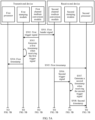
- FIG 2 is a schematic architectural diagram of a system according to an embodiment of the present invention.
- the system may include a transmit-end device 10 and a receive-end device 20.
- the system may use the 1588V2 protocol to synchronize time between the receive-end device 20 and the transmit-end device 10.
- the transmit-end device 10 includes a first channel medium conversion module 101, and the receive-end device 20 correspondingly includes a second channel medium conversion module 201.
- the transmit-end device 10 and the receive-end device 20 may transmit messages to each other.
- the messages generated by the transmit-end device 10 and the receive-end device 20 carry timestamps.
- the transmit-end device 10 and the receive-end device 20 each send the generated message to a local channel medium conversion module.
- a local channel medium conversion module in the local device needs to process the message.
- the transmit-end device 10 generates a message that carries a timestamp, and sends the message to the first channel medium conversion module 101.
- the first channel medium conversion module 101 coverts the message into a signal that can be transmitted in a transmission medium, and transfers the signal to the receive-end device 20 by using the transmission medium.
- the first channel medium conversion module 101 and the second channel medium conversion module 201 may be optical modules; and are configured to carry, on an optical wave, a message that carries a time stamp, and transmit the message to a peer-end device by using an optical fiber.
- the first channel medium conversion module 101 and the second channel medium conversion module 201 may be channel medium conversion modules of another type, for example, electromagnetic wave conversion modules; and are configured to carry a message on an electromagnetic wave (for example, a microwave), and transmit the message to a peer-end device. This is not limited in this embodiment.
- the 1588V2 protocol requires that a transmit delay be symmetrical to a receive delay.
- a transmit delay is symmetrical to a receive delay.
- a delay in a transmit link by which the transmit-end device 10 sends a message to the receive-end device 20 is the transmit delay
- a delay in a receive link by which the transmit-end device 10 receives a message sent by the receive-end device 20 is the receive delay.
- the transmit delay and the receive delay are collectively referred to as a link delay.
- a time span from a moment at which a message passes through a protocol stack and a timestamp is generated to a moment at which the message leaves the first channel medium conversion module 101 is a first time span
- a time span from a moment at which the message enters the first channel medium conversion module 101 to a moment at which the first channel medium conversion module 101 completes processing and the message enters the protocol stack is a second time span.
- the first time span needs to be equal to the second time span, or a difference between the first time span and the second time span needs to be constant.
- a transmit delay needs to be symmetrical to a receive delay.
- the first channel medium conversion module 101 and the second channel medium conversion module 201 differ in processing types and signal processing amounts concerning a transmitted signal and a received signal. Therefore, a transmit link delay is unequal to a receive link delay, and a difference between the transmit link delay and the receive link delay is inconstant. Therefore, precise time compensation cannot be performed, reducing time synchronization precision.
- stamping points for generating timestamps in the system are moved from physical layer (physical layer, PHY) chips in the transmit-end device 10 and the receive-end device 20 to the first channel medium conversion module 101 and the second channel medium conversion module 201.
- PHY physical layer
- the first channel medium conversion module 101 sends a header signal to the second medium conversion module 201, and at the same time, the transmit-end device 10 generates a first timestamp.
- a fourth timestamp may also be generated in the transmit-end device 10 when the first channel medium conversion module 101 receives a header signal sent by the receive-end device 20.
- a second timestamp is generated when the second channel medium conversion module 201 in the receive-end device 20 receives a header signal sent by the transmit-end device 10, and a third timestamp may also be generated in the receive-end device 20 when the second channel medium conversion module 201 sends a header signal to the transmit-end device 10.
- FIG 3 is a schematic structural diagram of a transmit-end device 10 according to an embodiment of the present invention.
- FIG 4 is a schematic structural diagram of a receive-end device 20 according to an embodiment of the present invention.
- the transmit-end device 10 further includes a first stamping module 102, a first processor 103, a media access control (media access control, MAC) chip 104, and a PHY chip 105.
- the receive-end device 20 further includes a second stamping module 202, a second processor 203, a MAC chip 204, and a PHY chip 205.
- a process of transmitting a message that carries a timestamp is as follows:
- the first stamping module 102 sends a generated timestamp to the first processor 103.
- the first processor 103 generates a message, and adds the timestamp to the message.
- the message is encapsulated by the MAC chip 104 and the PHY chip 105 in the transmit-end device 10, to obtain a data bit stream, and the data bit stream is sent to a first channel medium conversion module 101.
- the first channel medium conversion module 101 performs pre-transmission processing, such as channel coding, on the data bit stream; converts a processed data bit stream into a signal, for example, an optical signal, that can be transmitted on a transmission medium; and sends the signal to a second channel medium conversion module 201 in the receive-end device 20. After receiving the optical signal, the second channel medium conversion module 201 converts the optical signal into a data bit stream.
- the data bit stream is decapsulated by the PHY chip 205 and the MAC chip 204 and then sent to the second processor 203.
- a timestamp generation and transmission process in the receive-end device 20 is similar to that in the transmit-end device 10. Details are not described again.
- the first channel medium conversion module 101 may include a receiver 1012 and a transmitter 1011.
- the receiver 1012 and the transmitter 1011 may be integrated into one chip.
- the receiver 1012 is configured to receive a data bit stream sent by the receive-end device 20.
- the data bit stream is decapsulated, by the PHY chip 105 and the MAC chip 104, into a message that carries a timestamp; and the message is transmitted to the first processor 103.
- the receiver 1012 may further receive and identify a header signal, and send a trigger signal for triggering timestamping to the first stamping module 102.
- the transmitter 1011 is configured to receive the data bit stream processed by the MAC chip 104 and the PHY chip 105 in the transmit-end device 10, and send the data bit stream to the receive-end device 20.
- the transmitter 1011 is further configured to send a header signal to the receive-end device 20, and send a trigger signal for triggering stamping to the first stamping module 102.
- the first stamping module 102 may send
- the second channel medium conversion module 201 may include a receiver 2012 and a transmitter 2011.
- the receiver 2012 and the transmitter 2011 may be integrated into one chip.
- the receiver 2012 is configured to receive a data bit stream sent by the transmit-end device 10.
- the data bit stream is decapsulated, by the PHY chip 205 and the MAC chip 204, into a message that carries a timestamp; and the message is transmitted to the second processor 203.
- the receiver 2012 may further receive and identify a header signal, and send a trigger signal for triggering timestamping to the second stamping module 202.
- the transmitter 2011 is configured to receive the data bit stream processed by the MAC chip 204 and the PHY chip 205 in the receive-end device 20, and send the data bit stream to the transmit-end device 10.
- the transmitter 2011 is further configured to send a header signal to the transmit-end device 10, and send a trigger signal for triggering stamping to the second stamping module 202.
- the second stamping module 202 may send a timestamp to the second processor
- the first processor 103 and the second processor 203 each may be a central processing unit (central processing unit, CPU) or a network processor (network processor, NP).
- the first processor 103 and the second processor 203 are configured to generate and send messages, where the messages may include a synchronization message, a delay request message, and a delay response message.
- the first stamping module 102 and the second stamping module 202 are configured to generate timestamps.
- the first stamping module 102 may generate a timestamp when receiving a trigger signal sent by the first channel medium conversion module 101.
- the second stamping module 202 may generate a timestamp when receiving a trigger signal sent by the second channel medium conversion module 201.
- the first stamping module 102 and the second stamping module 202 each may be implemented by using, for example, a field programmable gate array (field programmable gate array, FPGA). All or some of components in each of the transmit-end device 10 and the receive-end device 20 may be integrated into one component or disposed separately as required.
- FPGA field programmable gate array
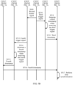
- FIG 5A and FIG 5B are a schematic flowchart of a time synchronization method according to an embodiment of the present invention. As shown in FIG 5A and FIG 5B , the time synchronization method may include the following steps.
- a first channel medium conversion module in a transmit-end device sends a first header signal to a receive-end device.
- the transmit-end device and the receive-end device continuously transmit data frames to each other.
- the data frames may be data frames of an existing service flow between the transmit-end device and the receive-end device.
- the transmit-end device may send a data frame to the receive-end device or receive a data frame from the receive-end device by using the first channel medium conversion module.
- the receive-end device may send a data frame to the transmit-end device or receive a data frame from the transmit-end device by using a second channel medium conversion module.
- a data frame includes a frame header.
- the transmit-end device and the receive-end device can identify the frame header in the received data frame.
- the first header signal may be a frame header of a data frame sent by the transmit-end device.
- the first channel medium conversion module in the transmit-end device sends a first trigger signal to a first stamping module.
- the first channel medium conversion module sends the first trigger signal to the first stamping module simultaneously when sending the first header signal to the second channel medium conversion module in the receive-end device.
- the first channel medium conversion module and the second channel medium conversion module each may be provided with a counter locally, to count a quantity of frame headers (namely, header signals) of data frames transmitted between the transmit-end device and the receive-end device.
- the following may be set in the transmit-end device and the receive-end device:
- the first channel medium conversion module detects that a quantity of transmitted header signals is a preset value N (in other words, detects the Nth header signal, where the Nth header signal is the transmitted first header signal)
- the first channel medium conversion module sends the first trigger signal to the first stamping module.
- the first channel medium conversion module detects that the quantity of transmitted header signals does not reach the preset value N, the first channel medium conversion module continues to send a header signal and counts an accumulative quantity of header signals.
- the second channel medium conversion module in the receive-end device detects that a quantity of received header signals sent by the first channel medium conversion module is the preset value N (in other words, detects that the Nth header signal is received, where the Nth header signal is the received first header signal)
- the second channel medium conversion module sends a second trigger signal to a second stamping module. If the second channel medium conversion module detects that the quantity of received header signals does not reach the preset value, the second channel medium conversion module continues to receive a header signal and counts an accumulative quantity of header signals.
- the preset value N may be 1 or a positive integer greater than 1.
- a channel medium conversion module sends one trigger signal to a local stamping module each time detecting 100 header signals.
- the first stamping module in the transmit-end device generates a first timestamp when receiving the first trigger signal.
- the first stamping module when receiving the first trigger signal, the first stamping module generates the first timestamp based on a system clock in the transmit-end device.
- the first timestamp indicates a first moment at which the first stamping module receives the first trigger signal, namely, a moment at which the first channel medium conversion module sends the first header signal.
- the first stamping module sends the first timestamp to a first processor.
- the first processor sends the first timestamp to the receive-end device.
- the first processor when receiving the first timestamp, the first processor generates a synchronization message, namely, a synchronization packet.
- the synchronization packet is a sync packet.
- a sync packet generated each time is used to carry a first timestamp generated in the current time.
- An originTimestamp field in the sync packet is used to carry the first timestamp, and other fields may be set correspondingly based on functions of the corresponding fields. This is not limited in this embodiment.
- the synchronization message that carries the first timestamp is encapsulated by a MAC chip and a PHY chip. This may include adding a MAC header; performing physical-layer code conversion, for example, physical coding sublayer (physical coding sublayer, PCS) processing; and the like.
- a data bit stream is obtained after the synchronization message that carries the first timestamp is encapsulated by the MAC chip and the PHY chip.
- the PHY chip sends the data bit stream to the first channel medium conversion module.
- the first channel medium conversion module converts the data bit stream, for example, performs channel coding on the data bit stream; and converts the data bit stream in a form of an electrical signal into a signal that can be transmitted between the first channel medium conversion module and the second channel medium conversion module.
- the first channel medium conversion module and the second channel medium conversion module may be optical modules. Then, the data bit stream in the form of an electrical signal is converted into an optical signal, and the optical signal is transmitted between the optical module in the transmit-end device and the optical module in the receive-end device by using an optical fiber. Alternatively, the optical signal may be transmitted to the receive-end device over the air. In this case, the optical signal is transmitted over the air.
- the first channel medium conversion module and the second channel medium conversion module may be configured to convert the data bit stream in the form of an electrical signal into a signal that can be transmitted in a transmission medium such as a copper wire, and transmit the signal in the transmission medium.
- the second channel medium conversion module in the receive-end device After receiving the signal sent by the first channel medium conversion module, the second channel medium conversion module in the receive-end device converts the signal into an electrical signal, namely, a data bit stream.
- the data bit stream is decapsulated by a PHY chip and a MAC chip, to restore the synchronization message, and the synchronization message is sent to a second processor.
- the second processor may store, in a memory of the receive-end device, the first timestamp extracted from the synchronization message.
- the first processor may generate a synchronization message periodically, and a generation period is the same as a trigger signal generation period.
- the synchronization message is used to carry a periodically updated first timestamp.
- the first processor may send a synchronization message that carries a first timestamp of a current time.
- the second channel medium conversion module sends the second trigger signal to the second stamping module.
- the second channel medium conversion module sends the second trigger signal to the second stamping module when receiving the first header signal.
- a counter may be embedded in the second channel medium conversion module, and is configured to count a quantity of received header signals.
- the second channel medium conversion module may generate the second trigger signal and send the second trigger signal to the second stamping module.
- the second stamping module generates a second timestamp when receiving the second trigger signal.
- the second stamping module when receiving the second trigger signal, the second stamping module generates the second timestamp based on a system clock in the receive-end device.
- the second timestamp indicates a second moment at which the second stamping module receives the second trigger signal, namely, a moment at which the second channel medium conversion module receives the first header signal.
- the second stamping module sends the second timestamp to the second processor.
- the second processor may store the second timestamp in the memory of the receive-end device.
- the second channel medium conversion module in the receive-end device sends a second header signal to the transmit-end device.
- the second header signal is similar to the first header signal, and may also be a frame header of a data frame transmitted between the transmit-end device and the receive-end device.
- the transmit-end device can identify a frame header of a data frame from the receive-end device.
- the second channel medium conversion module sends a third trigger signal to the second stamping module.
- the second channel medium conversion module sends the third trigger signal to the second stamping module while sending the second header signal to the transmit-end device.
- the second channel medium conversion module may include a counter for counting header signals.
- the second channel medium conversion module When detecting that a quantity of header signals sent by the second channel medium conversion module to the transmit-end device reaches a preset value M, the second channel medium conversion module generates and sends the third trigger signal.
- a process of generating the third trigger signal refer to step S502. Details are not described herein again.
- the second stamping module generates a third timestamp when receiving the third trigger signal.
- the second stamping module when receiving the third trigger signal, the second stamping module generates the third timestamp based on the system clock in the receive-end device.
- the third timestamp indicates a third moment at which the second stamping module receives the third trigger signal, namely, a moment at which the second channel medium conversion module sends the second header signal.
- the second stamping module sends the third timestamp to the second processor.
- the second processor may store the third timestamp in the memory of the receive-end device.
- the first channel medium conversion module sends a fourth trigger signal to the first stamping module.
- the first channel medium conversion module when the first channel medium conversion module receives the second header signal, the first channel medium conversion module sends the fourth trigger signal to the first stamping module.
- a counter may be embedded in the first channel medium conversion module, and is configured to count a quantity of received header signals.
- the first channel medium conversion module may generate the fourth trigger signal and send the fourth trigger signal to the first stamping module.
- the first stamping module generates a fourth timestamp when receiving the fourth trigger signal.
- the first stamping module when receiving the fourth trigger signal, the first stamping module generates the fourth timestamp based on the system clock in the transmit-end device.
- the fourth timestamp indicates a fourth moment at which the first stamping module receives the fourth trigger signal, namely, a moment at which the first channel medium conversion module receives the second header signal.
- the first stamping module sends the fourth timestamp to the first processor.
- the first processor sends the fourth timestamp to the receive-end device.
- the first processor when receiving the fourth timestamp, the first processor generates a delay response message, namely, a delay response packet.
- the delay response packet is a Delay_Resp packet.
- a Delay_Resp packet generated each time is used to carry a fourth timestamp generated in the current time.
- An originTimestamp field in the Delay _Resp packet may be used to carry the fourth timestamp.
- the delay response message that carries the fourth timestamp Before the first processor sends, to the receive-end device, the delay response message that carries the fourth timestamp, the delay response message that carries the fourth timestamp is encapsulated by the MAC chip and the PHY chip. This may include adding a MAC header; performing physical-layer code conversion, for example, PCS processing; and the like. A data bit stream is obtained after the delay response message that carries the fourth timestamp is encapsulated by the MAC chip and the PHY chip. The PHY chip sends the data bit stream to the first channel medium conversion module.
- the first channel medium conversion module converts the data bit stream, for example, performs channel coding on the data bit stream; and converts the data bit stream in a form of an electrical signal into a signal that can be transmitted between the first channel medium conversion module and the second channel medium conversion module.
- the first channel medium conversion module and the second channel medium conversion module may be optical modules. Then, the data bit stream in the form of an electrical signal is converted into an optical signal, and the optical signal is transmitted between the optical module in the transmit-end device and the optical module in the receive-end device by using an optical fiber. Alternatively, the optical signal may be transmitted to the receive-end device over the air. In this case, the optical signal is transmitted over the air.
- the first channel medium conversion module and the second channel medium conversion module may be configured to convert the data bit stream in the form of an electrical signal into a signal that can be transmitted in a transmission medium such as a copper wire, and transmit the signal in the transmission medium.
- the second channel medium conversion module in the receive-end device converts the signal into an electrical signal, namely, a data bit stream. Then the data bit stream is decapsulated by the PHY chip and the MAC chip, to restore the delay response message; and the delay response message is sent to the second processor.
- the second processor may store the fourth timestamp in the memory of the receive-end device.
- the receive-end device synchronizes time with the transmit-end device based on the first moment, the second moment, the third moment, and the fourth moment.
- the receive-end device synchronizes time with the transmit-end device based on the first moment, the second moment, the third moment, and the fourth moment that are respectively indicated by the first timestamp, the second timestamp, the third timestamp, and the fourth timestamp.
- first timestamp, the second timestamp, the third timestamp, and the fourth timestamp are respectively information, for example, character strings or coded information, indicating the first moment, the second moment, the third moment, and the fourth moment.
- the first channel medium conversion module in the transmit-end device when receiving or sending a header signal, sends a trigger signal for triggering timestamping to the first stamping module, and the first stamping module generates a timestamp; or when receiving or sending a header signal, the second channel medium conversion module in the receive-end device sends a trigger signal for triggering timestamping to the second stamping module, and the second stamping module generates a timestamp.
- a stamping point on a physical layer is moved to the channel medium conversion modules, so that a moment indicated by a timestamp is closer to a moment at which a signal enters or leaves a transmission medium. This reduces an uncertainty about a delay of transmitting a message between a stamping point and a physical layer medium and can improve precision of a timestamping moment, thereby improving precision of time synchronization between the receive-end device and the transmit-end device.
- FIG 6 is a schematic structural diagram of another receive-end device 20 according to an embodiment of the present invention.
- the receive-end device 20 may include a communications unit 601 and a processing unit 602.
- the communications unit 601 is configured to receive a first timestamp sent by a transmit-end device 10, and receive a first header signal sent by the transmit-end device 10, where the first header signal is sent by a first channel medium conversion module in the transmit-end device 10, the first timestamp indicates a first moment at which the first channel medium conversion module sends the first header signal, and a moment at which the receive-end device 20 receives the first header signal is a second moment;
- the first moment is a moment at which a first stamping module in the transmit-end device 10 receives a first trigger signal sent by the first channel medium conversion module
- the second moment is a moment at which a second stamping module in the receive-end device 20 receives a second trigger signal sent by the second channel medium conversion module
- the third moment is a moment at which the second stamping module receives a third trigger signal sent by the second channel medium conversion module
- the fourth moment is a moment at which the first stamping module receives a fourth trigger signal sent by the first channel medium conversion module.
- the first header signal is received by the second channel medium conversion module, and after the second channel medium conversion module receives the first header signal sent by the first channel medium conversion module, the second channel medium conversion module sends the second trigger signal to the second stamping module; and when the second stamping module receives the second trigger signal, the second stamping module generates a second timestamp and sends the second timestamp to a second processor in the receive-end device 20, where the second timestamp indicates the second moment.
- the second channel medium conversion module after the second channel medium conversion module sends the second header signal to the first channel medium conversion module, the second channel medium conversion module sends the third trigger signal to the second stamping module; and the second stamping module generates a third timestamp when the second stamping module receives the third trigger signal, and sends the third timestamp to the second processor in the receive-end device, where the third timestamp indicates the third moment.
- the communications unit 601 may be configured to implement the functions of the second channel medium conversion module, and the processing unit 602 may be configured to implement the functions of the second processor and the second stamping module.
- FIG 7 is a schematic structural diagram of another transmit-end device 10 according to an embodiment of the present invention.
- the transmit-end device 10 may include a communications unit 701 and a processing unit 702.
- the communications unit 701 is configured to send a first timestamp and a first header signal to a receive-end device 20, where the first header signal is sent by a first channel medium conversion module in the transmit-end device 10, the first timestamp indicates a first moment at which the first channel medium conversion module sends the first header signal, and a moment at which the receive-end device 20 receives the first header signal is a second moment.
- the communications unit 701 is further configured to receive a second header signal sent by the receive-end device 20, where the second header signal is sent by a second channel medium conversion module in the receive-end device 20, a moment at which the receive-end device 20 sends the second header signal is a third moment, and a moment at which the transmit-end device 10 receives the second header signal is a fourth moment.
- the communications unit 701 is further configured to send a fourth timestamp to the receive-end device 20, so that the receive-end device 20 can synchronize time with the transmit-end device 10 based on the first moment, the second moment, the third moment, and the fourth moment, where the fourth timestamp indicates the fourth moment.
- the processing unit 702 is configured to communicate with the communications unit 701.
- the first moment is a moment at which a first stamping module in the transmit-end device 10 receives a first trigger signal sent by the first channel medium conversion module
- the second moment is a moment at which a second stamping module in the receive-end device 20 receives a second trigger signal sent by the second channel medium conversion module
- the third moment is a moment at which the second stamping module receives a third trigger signal sent by the second channel medium conversion module
- the fourth moment is a moment at which the first stamping module receives a fourth trigger signal sent by the first channel medium conversion module.
- the communications unit 701 after the communications unit 701 sends the first header signal to the second channel medium conversion module, the communications unit 701 is further configured to send the first trigger signal to the first stamping module; and the processing unit 702 is further configured to generate the first timestamp when receiving the first trigger signal.
- the communications unit 701 is further configured to send the fourth trigger signal to the first stamping module after the first channel medium conversion module receives the second header signal sent by the second channel medium conversion module; and the processing unit 702 is further configured to generate the fourth timestamp when receiving the fourth trigger signal.
- the communications unit 701 sends a first timestamp to a receive-end device includes: the processing unit 702 is configured to: after receiving the first timestamp sent by the first stamping module, send a synchronization message to the receive-end device by using the first channel medium conversion module, where the synchronization message carries the first timestamp.
- the transmit-end device sends the fourth timestamp to the receive-end device includes: a first processor in the transmit-end device sends, after receiving the fourth timestamp sent by the first stamping module, a delay response message to the receive-end device by using the first channel medium conversion module, where the delay response message carries the fourth timestamp.
- the communications unit 701 may be configured to implement the functions of the first channel medium conversion module, and the processing unit 702 may be configured to implement the functions of the first processor and the first stamping module.
- FIG 8 is a schematic structural diagram of still another receive-end device 20 according to an embodiment of the present invention.
- the receive-end device 20 may include a second processor 801 and a second channel medium conversion module 802. A communication connection is established between the second processor 801 and the second channel medium conversion module 802.
- the second channel medium conversion module 802 is configured to receive a first timestamp sent by a transmit-end device and receive a first header signal sent by the transmit-end device, where the first header signal is sent by a first channel medium conversion module in the transmit-end device, the first timestamp indicates a first moment at which the first channel medium conversion module sends the first header signal, and a moment at which the receive-end device receives the first header signal is a second moment.
- the second channel medium conversion module 802 is further configured to send a second header signal to the transmit-end device, where a moment at which the second channel medium conversion module 802 sends the second header signal is a third moment.
- the second channel medium conversion module 802 is further configured to receive a fourth timestamp sent by the transmit-end device, where the fourth timestamp indicates a fourth moment at which the transmit-end device receives the second header signal.
- the second processor 801 is configured to synchronize time with the transmit-end device based on the first moment, the second moment, the third moment, and the fourth moment.
- the receive-end device further includes a second stamping module 803, the first moment is a moment at which a first stamping module in the transmit-end device 10 receives a first trigger signal sent by the first channel medium conversion module, the second moment is a moment at which the second stamping module 803 in the receive-end device 20 receives a second trigger signal sent by the second channel medium conversion module 802, the third moment is a moment at which the second stamping module 803 receives a third trigger signal sent by the second channel medium conversion module 802, and the fourth moment is a moment at which the first stamping module receives a fourth trigger signal sent by the first channel medium conversion module.
- the first moment is a moment at which a first stamping module in the transmit-end device 10 receives a first trigger signal sent by the first channel medium conversion module
- the second moment is a moment at which the second stamping module 803 in the receive-end device 20 receives a second trigger signal sent by the second channel medium conversion module 802
- the third moment is a moment at which the second stamping module
- the second channel medium conversion module 802 after the second channel medium conversion module 802 receives the first header signal sent by the first channel medium conversion module, the second channel medium conversion module 802 is further configured to send the second trigger signal to the second stamping module; and the second stamping module 803 is configured to generate a second timestamp when receiving the second trigger signal, and send the second timestamp to the second processor 801, where the second timestamp indicates the second moment.
- the second channel medium conversion module 802 after the second channel medium conversion module 802 sends the second header signal to the first channel medium conversion module, the second channel medium conversion module 802 is further configured to send the third trigger signal to the second stamping module 803; and the second stamping module 803 is further configured to generate a third timestamp when receiving the third trigger signal, and send the third timestamp to the second processor 801, where the third timestamp indicates the third moment.
- each module refers to corresponding descriptions in the embodiment of the time synchronization method shown in FIG 5A and FIG 5B .
- FIG 9 is a schematic structural diagram of still another transmit-end device 10 according to an embodiment of the present invention.
- the transmit-end device 10 may include a first processor 901 and a first channel medium conversion module 902. A communication connection is established between the first processor 901 and the first channel medium conversion module 902.
- the first channel medium conversion module 902 is configured to send a first timestamp to a receive-end device and send a first header signal to the receive-end device, where the first header signal is sent by the first channel medium conversion module 902 in the transmit-end device, the first timestamp indicates a first moment at which the first channel medium conversion module 902 sends the first header signal, and a moment at which the receive-end device receives the first header signal is a second moment.
- the first channel medium conversion module 902 is further configured to receive a second header signal sent by the receive-end device, where the second header signal is sent by a second channel medium conversion module in the receive-end device, a moment at which the receive-end device sends the second header signal is a third moment, and a moment at which the transmit-end device 10 receives the second header signal is a fourth moment.
- the first channel medium conversion module 902 is further configured to send a fourth timestamp to the receive-end device, so that the receive-end device can synchronize time with the transmit-end device based on the first moment, the second moment, the third moment, and the fourth moment, where the fourth timestamp indicates the fourth moment.
- the first processor 901 is configured to communicate with the first channel medium conversion module 902.
- the transmit-end device 10 further includes a first stamping module 903, the first moment is a moment at which the first stamping module 903 receives a first trigger signal sent by the first channel medium conversion module 902, the second moment is a moment at which a second stamping module in the receive-end device receives a second trigger signal sent by the second channel medium conversion module, the third moment is a moment at which the second stamping module receives a third trigger signal sent by the second channel medium conversion module, and the fourth moment is a moment at which the first stamping module 903 receives a fourth trigger signal sent by the first channel medium conversion module 902.
- the first channel medium conversion module 902 after the first channel medium conversion module 902 sends the first header signal to the second channel medium conversion module, the first channel medium conversion module 902 is further configured to send the first trigger signal to the first stamping module 903; and the first stamping module 903 is configured to generate the first timestamp when receiving the first trigger signal, and send the first timestamp to the first processor 901.
- the first channel medium conversion module 902 is further configured to send the fourth trigger signal to the first stamping module 903 after receiving the second header signal sent by the second channel medium conversion module; and the first stamping module 903 is further configured to generate the fourth timestamp when receiving the fourth trigger signal, and send the fourth timestamp to the first processor 901.
- the first channel medium conversion module 902 is configured to send a first timestamp to a receive-end device includes: the first processor 901 sends, after receiving the first timestamp sent by the first stamping module, a synchronization message to the receive-end device by using the first channel medium conversion module, where the synchronization message carries the first timestamp.
- the first channel medium conversion module 902 is further configured to send a fourth timestamp to the receive-end device includes: the first processor in the transmit-end device 10 sends, after receiving the fourth timestamp sent by the first stamping module 903, a delay response message to the receive-end device by using the first channel medium conversion module 902, where the delay response message carries the fourth timestamp.
- an embodiment of the present invention provides a communications system.
- the communications system includes a transmit-end device 10 and a receive-end device 20.
- the receive-end device 20 is one of the receive-end device provided in the embodiment described in FIG 3 , the receive-end device provided in the embodiment described in FIG 6 , or the receive-end device provided in the embodiment described in FIG 8 .
- the transmit-end device 10 is one of the transmit-end device provided in the embodiment described in FIG 4 , the transmit-end device provided in the embodiment described in FIG 7 , or the receive-end device provided in the embodiment described in FIG 9 .
- each module refers to corresponding descriptions in the embodiment of the time synchronization method shown in FIG 5A and FIG 5B .
- the embodiments of the present invention may be provided as a method, a system, or a computer program product. Therefore, all or some of the embodiments of the present invention may be implemented by using software, hardware, firmware, or any combination thereof. Moreover, the embodiments of the present invention may use a form of a computer program product that is implemented on one or more computer-usable storage media (including but not limited to a disk memory, an optical memory, and the like) that include computer-usable program code.
- computer-usable storage media including but not limited to a disk memory, an optical memory, and the like
- These computer program instructions may be provided for a general-purpose computer, a dedicated computer, an embedded processor, or a processor of any other programmable data processing device to generate a machine, so that the instructions executed by a computer or a processor of any other programmable data processing device generate an apparatus for implementing a specific function in one or more processes in the flowcharts and/or in one or more blocks in the block diagrams.
- These computer program instructions may also be stored in a computer readable memory that can instruct the computer or any other programmable data processing device to work in a specific manner, so that the instructions stored in the computer readable memory generate an artifact that includes an instruction apparatus.
- the instruction apparatus implements a specific function in one or more processes in the flowcharts and/or in one or more blocks in the block diagrams.
- These computer program instructions may also be loaded onto a computer or another programmable data processing device, so that a series of operations and steps are performed on the computer or the another programmable device, thereby generating computer-implemented processing. Therefore, the instructions executed on the computer or the another programmable device provide steps for implementing a specific function in one or more processes in the flowcharts and/or in one or more blocks in the block diagrams.
- the program may be stored in a computer readable storage medium. When the program runs, the processes of the method embodiments are performed.
- the foregoing storage medium includes any medium that can store program code, such as a ROM, a random access memory RAM, a magnetic disk, or an optical disc.
Landscapes
- Engineering & Computer Science (AREA)
- Computer Networks & Wireless Communication (AREA)
- Signal Processing (AREA)
- Synchronisation In Digital Transmission Systems (AREA)
- Data Exchanges In Wide-Area Networks (AREA)
Claims (15)
- Zeitsynchronisationsverfahren, umfassend:Empfangen, durch eine Empfangsendevorrichtung (20), eines ersten Zeitstempels, der durch eine Übertragungsendevorrichtung (10) gesendet wird, und Empfangen eines ersten Header-Signals, das durch die Übertragungsendevorrichtung (10) gesendet wird, wobei das erste Header-Signal auf einem Übertragungsmedium durch ein erstes Kanalmediumumwandlungsmodul (101) in der Übertragungsendevorrichtung (10) gesendet wird, wobei das erste Kanalmediumumwandlungsmodul (101) von einem Chip einer physikalischen Schicht, PHY-Chip, (105) in der Übertragungsendevorrichtung (10) getrennt ist, der erste Zeitstempel einen ersten Zeitpunkt angibt, zu dem das erste Kanalmediumumwandlungsmodul das erste Header-Signal sendet, und ein Zeitpunkt, zu dem die Empfangsendevorrichtung (20) das erste Header-Signal empfängt, ein zweiter Zeitpunkt ist;Senden, durch die Empfangsendevorrichtung (20), eines zweiten Header-Signals an die Übertragungsendevorrichtung (10), wobei das zweite Header-Signal auf dem Übertragungsmedium durch ein zweites Kanalmediumumwandlungsmodul (201) in der Empfangsendevorrichtung (20) gesendet wird, wobei das zweite Kanalmediumumwandlungsmodul (201) von einem Chip einer physikalischen Schicht, PHY-Chip, (205) in der Empfangsendevorrichtung (20) getrennt ist und ein Zeitpunkt, zu dem die Empfangsendevorrichtung (20) das zweite Header-Signal sendet, ein dritter Zeitpunkt ist;Empfangen, durch die Empfangsendevorrichtung (20), eines vierten Zeitstempels, der durch die Übertragungsendevorrichtung (10) gesendet wird, wobei der vierte Zeitstempel einen vierten Zeitpunkt angibt, zu dem die Übertragungsendevorrichtung (10) das zweite Header-Signal empfängt; undSynchronisieren, durch die Empfangsendevorrichtung (20), von Zeit mit der Übertragungsendevorrichtung (10) basierend auf dem ersten Zeitpunkt, dem zweiten Zeitpunkt, dem dritten Zeitpunkt und dem vierten Zeitpunkt.
- Zeitsynchronisierungsverfahren nach Anspruch 1, wobei der erste Zeitpunkt ein Zeitpunkt ist, zu dem ein erstes Stempelmodul in der Übertragungsendevorrichtung ein erstes Auslösesignal empfängt, das durch das erste Kanalmediumumwandlungsmodul gesendet wird, der zweite Zeitpunkt ein Zeitpunkt ist, zu dem ein zweites Stempelmodul in der Empfangsendevorrichtung ein zweites Auslösesignal empfängt, das durch das zweite Kanalmediumumwandlungsmodul gesendet wird, der dritte Zeitpunkt ein Zeitpunkt ist, zu dem das zweite Stempelmodul ein drittes Auslösesignal empfängt, das durch das zweite Kanalmediumumwandlungsmodul gesendet wird, und der vierte Zeitpunkt ein Zeitpunkt ist, zu dem das erste Stempelmodul ein viertes Auslösesignal empfängt, das durch das erste Kanalmediumumwandlungsmodul gesendet wird.
- Verfahren nach Anspruch 2, wobei das erste Header-Signal durch das zweite Kanalmediumumwandlungsmodul empfangen wird, und, nachdem das zweite Kanalmediumumwandlungsmodul das erste Header-Signal empfängt, das durch das erste Kanalmediumumwandlungsmodul gesendet wird, das Verfahren ferner Folgendes umfasst:Senden, durch das zweite Kanalmediumumwandlungsmodul, des zweiten Auslösesignals an das zweite Stempelmodul; undErzeugen, durch das zweite Stempelmodul, eines zweiten Zeitstempels, wenn das zweite Stempelmodul das zweite Auslösesignal empfängt, und Senden des zweiten Zeitstempels an einen Prozessor in der Empfangsendevorrichtung, wobei der zweite Zeitstempel den zweiten Zeitpunkt angibt.
- Verfahren nach Anspruch 2 oder 3, wobei, nachdem das zweite Kanalmediumumwandlungsmodul das zweite Header-Signal an das erste Kanalmediumumwandlungsmodul sendet, das Verfahren ferner Folgendes umfasst:Senden, durch das zweite Kanalmediumumwandlungsmodul, des dritten Auslösesignals an das zweite Stempelmodul; undErzeugen, durch das zweite Stempelmodul, eines dritten Zeitstempels, wenn das zweite Stempelmodul das dritte Auslösesignal empfängt, und Senden des dritten Zeitstempels an einen Prozessor in der Empfangsendevorrichtung, wobei der dritte Zeitstempel den dritten Zeitpunkt angibt.
- Zeitsynchronisationsverfahren, umfassend:Senden, durch eine Übertragungsendevorrichtung (10), eines ersten Zeitstempels an eine Empfangsendevorrichtung (20) und Senden eines ersten Header-Signals an die Empfangsendevorrichtung (20), wobei das erste Header-Signal auf einem Übertragungsmedium durch ein erstes Kanalmediumumwandlungsmodul (101) in der Übertragungsendevorrichtung (10) gesendet wird, wobei das erste Kanalmediumumwandlungsmodul (101) von einem Chip einer physikalischen Schicht, PHY-Chip, (105) in der Übertragungsendevorrichtung (10) getrennt ist, der erste Zeitstempel einen ersten Zeitpunkt angibt, zu dem das erste Kanalmediumumwandlungsmodul das erste Header-Signal sendet, und ein Zeitpunkt, zu dem die Empfangsendevorrichtung (20) das erste Header-Signal empfängt, ein zweiter Zeitpunkt ist;Empfangen, durch die Übertragungsendevorrichtung (10), eines zweiten Header-Signals, das durch die Empfangsendevorrichtung (20) gesendet wird, wobei das zweite Header-Signal auf dem Übertragungsmedium durch ein zweites Kanalmediumumwandlungsmodul (201) in der Empfangsendevorrichtung (20) gesendet wird, wobei das zweite Kanalmediumumwandlungsmodul (201) von einem Chip einer physikalischen Schicht, PHY-Chip, (205) in der Empfangsendevorrichtung (20) getrennt ist, ein Zeitpunkt, zu dem die Empfangsendevorrichtung (20) das zweite Header-Signal sendet, ein dritter Zeitpunkt ist und ein Zeitpunkt, zu dem die Übertragungsendevorrichtung (10) das zweite Header-Signal empfängt, ein vierter Zeitpunkt ist; undSenden, durch die Übertragungsendevorrichtung (10), eines vierten Zeitstempels an die Empfangsendevorrichtung (20), sodass die Empfangsendevorrichtung (20) Zeit mit der Übertragungsendevorrichtung (10) basierend auf dem ersten Zeitpunkt, dem zweiten Zeitpunkt, dem dritten Zeitpunkt und dem vierten Zeitpunkt synchronisieren kann, wobei der vierte Zeitstempel den vierten Zeitpunkt angibt.
- Zeitsynchronisierungsverfahren nach Anspruch 5, wobei der erste Zeitpunkt ein Zeitpunkt ist, zu dem ein erstes Stempelmodul in der Übertragungsendevorrichtung ein erstes Auslösesignal empfängt, das durch das erste Kanalmediumumwandlungsmodul gesendet wird, der zweite Zeitpunkt ein Zeitpunkt ist, zu dem ein zweites Stempelmodul in der Empfangsendevorrichtung ein zweites Auslösesignal empfängt, das durch das zweite Kanalmediumumwandlungsmodul gesendet wird, der dritte Zeitpunkt ein Zeitpunkt ist, zu dem das zweite Stempelmodul ein drittes Auslösesignal empfängt, das durch das zweite Kanalmediumumwandlungsmodul gesendet wird, und der vierte Zeitpunkt ein Zeitpunkt ist, zu dem das erste Stempelmodul ein viertes Auslösesignal empfängt, das durch das erste Kanalmediumumwandlungsmodul gesendet wird.
- Verfahren nach Anspruch 6, wobei, nachdem das erste Kanalmediumumwandlungsmodul das erste Header-Signal an das zweite Kanalmediumumwandlungsmodul sendet, das Verfahren ferner Folgendes umfasst:Senden, durch das erste Kanalmediumumwandlungsmodul, des ersten Auslösesignals an das erste Stempelmodul; undErzeugen, durch das erste Stempelmodul, des ersten Zeitstempels, wenn das erste Stempelmodul das erste Auslösesignal empfängt, und Senden des ersten Zeitstempels an einen Prozessor in der Übertragungsendevorrichtung.
- Verfahren nach Anspruch 6 oder 7, wobei das zweite Header-Signal durch das erste Kanalmediumumwandlungsmodul empfangen wird, und, nachdem das erste Kanalmediumumwandlungsmodul das zweite Header-Signal empfängt, das durch das zweite Kanalmediumumwandlungsmodul gesendet wird, das Verfahren ferner Folgendes umfasst:Senden, durch das erste Kanalmediumumwandlungsmodul, des vierten Auslösesignals an das erste Stempelmodul; undErzeugen, durch das erste Stempelmodul, des vierten Zeitstempels, wenn das erste Stempelmodul das vierte Auslösesignal empfängt, und Senden des vierten Zeitstempels an den Prozessor in der Übertragungsendevorrichtung.
- Empfangsendevorrichtung (20), umfassend einen Prozessor und ein zweites Kanalmediumumwandlungsmodul (201), wobei das zweite Kanalmediumumwandlungsmodul (201) von einem Chip einer physikalischen Schicht, PHY-Chip, (205) in der Empfangsendevorrichtung (20) getrennt ist, und wobeidas zweite Kanalmediumumwandlungsmodul dazu konfiguriert ist, einen ersten Zeitstempel zu empfangen, der durch eine Übertragungsendevorrichtung (10) gesendet wird, und ein erstes Header-Signal zu empfangen, das auf einem Übertragungsmedium durch die Übertragungsendevorrichtung (10) gesendet wird, wobei das erste Header-Signal durch ein erstes Kanalmediumumwandlungsmodul in der Übertragungsendevorrichtung (10) gesendet wird, der erste Zeitstempel einen ersten Zeitpunkt angibt, zu dem das erste Kanalmediumumwandlungsmodul das erste Header-Signal sendet, und ein Zeitpunkt, zu dem die Empfangsendevorrichtung (20) das erste Header-Signal empfängt, ein zweiter Zeitpunkt ist;das zweite Kanalmediumumwandlungsmodul ferner dazu konfiguriert ist, auf dem Übertragungsmedium ein zweites Header-Signal an die Übertragungsendevorrichtung (10) zu senden, wobei ein Zeitpunkt, zu dem das zweite Kanalmediumumwandlungsmodul das zweite Header-Signal sendet, ein dritter Zeitpunkt ist;das zweite Kanalmediumumwandlungsmodul ferner dazu konfiguriert ist, einen vierten Zeitstempel zu empfangen, der durch die Übertragungsendevorrichtung (10) gesendet wird, wobei der vierte Zeitstempel einen vierten Zeitpunkt angibt, zu dem die Übertragungsendevorrichtung (10) das zweite Header-Signal empfängt; undder Prozessor dazu konfiguriert ist, Zeit mit der Übertragungsendevorrichtung (10) basierend auf dem ersten Zeitpunkt, dem zweiten Zeitpunkt, dem dritten Zeitpunkt und dem vierten Zeitpunkt zu synchronisieren.
- Empfangsendevorrichtung nach Anspruch 9, wobei die Empfangsendevorrichtung ferner ein zweites Stempelmodul umfasst, der erste Zeitpunkt ein Zeitpunkt ist, zu dem ein erstes Stempelmodul in der Übertragungsendevorrichtung ein erstes Auslösesignal empfängt, das durch das erste Kanalmediumumwandlungsmodul gesendet wird, der zweite Zeitpunkt ein Zeitpunkt ist, zu dem das zweite Stempelmodul in der Empfangsendevorrichtung ein zweites Auslösesignal empfängt, das durch das zweite Kanalmediumumwandlungsmodul gesendet wird, der dritte Zeitpunkt ein Zeitpunkt ist, zu dem das zweite Stempelmodul ein drittes Auslösesignal empfängt, das durch das zweite Kanalmediumumwandlungsmodul gesendet wird, und der vierte Zeitpunkt ein Zeitpunkt ist, zu dem das erste Stempelmodul ein viertes Auslösesignal empfängt, das durch das erste Kanalmediumumwandlungsmodul gesendet wird.
- Empfangsendevorrichtung nach Anspruch 10, wobei, nachdem das zweite Kanalmediumumwandlungsmodul das erste Header-Signal empfängt, das durch das erste Kanalmediumumwandlungsmodul gesendet wird, das zweite Kanalmediumumwandlungsmodul ferner dazu konfiguriert ist, das zweite Auslösesignal an das zweite Stempelmodul zu senden; und
das zweite Stempelmodul dazu konfiguriert ist, einen zweiten Zeitstempel zu erzeugen, wenn es das zweite Auslösesignal empfängt, und den zweiten Zeitstempel an den Prozessor zu senden, wobei der zweite Zeitstempel den zweiten Zeitpunkt angibt. - Übertragungsendevorrichtung (10), umfassend einen Prozessor und ein erstes Kanalmediumumwandlungsmodul (101), wobei das erste Kanalmediumumwandlungsmodul (101) von einem Chip einer physikalischen Schicht, PHY-Chip, (105) in der Übertragungsendevorrichtung (10) getrennt ist und wobeidas erste Kanalmediumumwandlungsmodul dazu konfiguriert ist, einen ersten Zeitstempel an eine Empfangsendevorrichtung (20) zu senden und ein erstes Header-Signal an die Empfangsendevorrichtung (20) zu senden, wobei das erste Header-Signal auf einem Übertragungsmedium durch das erste Kanalmediumumwandlungsmodul in der Übertragungsendevorrichtung (10) gesendet wird, der erste Zeitstempel einen ersten Zeitpunkt angibt, zu dem das erste Kanalmediumumwandlungsmodul das erste Header-Signal sendet, und ein Zeitpunkt, zu dem die Empfangsendevorrichtung (20) das erste Header-Signal empfängt, ein zweiter Zeitpunkt ist;das erste Kanalmediumumwandlungsmodul ferner dazu konfiguriert ist, ein zweites Header-Signal zu empfangen, das durch die Empfangsendevorrichtung (20) gesendet wird, wobei das zweite Header-Signal auf dem Übertragungsmedium durch ein zweites Kanalmediumumwandlungsmodul in der Empfangsendevorrichtung (20) gesendet wird, ein Zeitpunkt, zu dem die Empfangsendevorrichtung (20) das zweite Header-Signal sendet, ein dritter Zeitpunkt ist und ein Zeitpunkt, zu dem die Übertragungsendevorrichtung (10) das zweite Header-Signal empfängt, ein vierter Zeitpunkt ist;das erste Kanalmediumumwandlungsmodul ferner dazu konfiguriert ist, einen vierten Zeitstempel an die Empfangsendevorrichtung (20) zu senden, sodass die Empfangsendevorrichtung (20) Zeit mit der Übertragungsendevorrichtung (10) basierend auf dem ersten Zeitpunkt, dem zweiten Zeitpunkt, dem dritten Zeitpunkt und dem vierten Zeitpunkt synchronisieren kann, wobei der vierte Zeitstempel den vierten Zeitpunkt angibt; undder Prozessor dazu konfiguriert ist, mit dem ersten Kanalmediumumwandlungsmodul zu kommunizieren.
- Übertragungsendevorrichtung nach Anspruch 12, wobei die Übertragungsendevorrichtung ferner ein erstes Stempelmodul umfasst, der erste Zeitpunkt ein Zeitpunkt ist, zu dem das erste Stempelmodul ein erstes Auslösesignal empfängt, das durch das erste Kanalmediumumwandlungsmodul gesendet wird, der zweite Zeitpunkt ein Zeitpunkt ist, zu dem ein zweites Stempelmodul in der Empfangsendevorrichtung ein zweites Auslösesignal empfängt, das durch das zweite Kanalmediumumwandlungsmodul gesendet wird, der dritte Zeitpunkt ein Zeitpunkt ist, zu dem das zweite Stempelmodul ein drittes Auslösesignal empfängt, das durch das zweite Kanalmediumumwandlungsmodul gesendet wird, und der vierte Zeitpunkt ein Zeitpunkt ist, zu dem das erste Stempelmodul ein viertes Auslösesignal empfängt, das durch das erste Kanalmediumumwandlungsmodul gesendet wird.
- Übertragungsendevorrichtung nach Anspruch 13, wobei, nachdem das erste Kanalmediumumwandlungsmodul das erste Header-Signal an das zweite Kanalmediumumwandlungsmodul sendet, das erste Kanalmediumumwandlungsmodul ferner dazu konfiguriert ist, das erste Auslösesignal an das erste Stempelmodul zu senden; und das erste Stempelmodul dazu konfiguriert ist, den ersten Zeitstempel zu erzeugen, wenn es das erste Auslösesignal empfängt, und den ersten Zeitstempel an den Prozessor in der Übertragungsendevorrichtung zu senden.
- Übertragungsendevorrichtung nach Anspruch 13 oder 14, wobei das erste Kanalmediumumwandlungsmodul ferner dazu konfiguriert ist, das vierte Auslösesignal an das erste Stempelmodul zu senden, nachdem es das zweite Header-Signal empfängt, das durch das zweite Kanalmediumumwandlungsmodul gesendet wird; und
das erste Stempelmodul ferner dazu konfiguriert ist, den vierten Zeitstempel zu erzeugen, wenn es das vierte Auslösesignal empfängt, und den vierten Zeitstempel an den Prozessor in der Übertragungsendevorrichtung zu senden.
Applications Claiming Priority (1)
| Application Number | Priority Date | Filing Date | Title |
|---|---|---|---|
| PCT/CN2017/091267 WO2019000432A1 (zh) | 2017-06-30 | 2017-06-30 | 时间同步方法及设备 |
Publications (3)
| Publication Number | Publication Date |
|---|---|
| EP3637640A1 EP3637640A1 (de) | 2020-04-15 |
| EP3637640A4 EP3637640A4 (de) | 2020-05-20 |
| EP3637640B1 true EP3637640B1 (de) | 2024-11-27 |
Family
ID=64741967
Family Applications (1)
| Application Number | Title | Priority Date | Filing Date |
|---|---|---|---|
| EP17916220.1A Active EP3637640B1 (de) | 2017-06-30 | 2017-06-30 | Zeitsynchronisationsverfahren und -vorrichtung |
Country Status (4)
| Country | Link |
|---|---|
| US (1) | US11343007B2 (de) |
| EP (1) | EP3637640B1 (de) |
| CN (2) | CN109429553B (de) |
| WO (1) | WO2019000432A1 (de) |
Families Citing this family (2)
| Publication number | Priority date | Publication date | Assignee | Title |
|---|---|---|---|---|
| CN111464252B (zh) * | 2019-01-22 | 2023-01-06 | 华为技术有限公司 | 通信方法和光模块 |
| CN110071851B (zh) * | 2019-04-19 | 2022-01-25 | 成都飞机工业(集团)有限责任公司 | 一种测量飞行试验数据延迟的系统及方法 |
Citations (1)
| Publication number | Priority date | Publication date | Assignee | Title |
|---|---|---|---|---|
| US20140177653A1 (en) * | 2012-12-20 | 2014-06-26 | Broadcom Corporation | Inband Timestamping |
Family Cites Families (12)
| Publication number | Priority date | Publication date | Assignee | Title |
|---|---|---|---|---|
| JP4899087B2 (ja) * | 2006-03-24 | 2012-03-21 | 富士通株式会社 | 伝送システム |
| CN101499871B (zh) * | 2008-02-03 | 2013-02-13 | 大唐移动通信设备有限公司 | Sdh网元时延检测方法、时钟同步方法及sdh网元 |
| CN102957489B (zh) * | 2008-02-03 | 2015-04-01 | 大唐移动通信设备有限公司 | 时钟同步方法、主从时钟实体 |
| CN101547083B (zh) * | 2008-03-24 | 2011-12-21 | 杭州华三通信技术有限公司 | 时间同步装置、时间同步系统和时间同步方法 |
| CN102130735A (zh) * | 2010-11-09 | 2011-07-20 | 华为技术有限公司 | 一种传送设备及其实现时钟和时间同步的方法 |
| CN202772918U (zh) * | 2011-11-29 | 2013-03-06 | 浙江省电力公司 | 一种ptp信号协议转换设备 |
| CN102387155B (zh) * | 2011-11-29 | 2014-08-06 | 浙江省电力公司 | 一种延迟恒定的ptp信号协议转换系统及实现方法 |
| CN104380632B (zh) * | 2012-06-26 | 2018-04-24 | 马维尔国际贸易有限公司 | 用于精确加时间戳的方法和装置 |
| WO2014006446A1 (en) * | 2012-07-02 | 2014-01-09 | Freescale Semiconductor, Inc. | Ethercat packet forwarding with distributed clocking |
| US9184861B2 (en) * | 2013-10-01 | 2015-11-10 | Khalifa University of Science, Technology, and Research | Method and devices for synchronization |
| US9306693B2 (en) * | 2013-11-15 | 2016-04-05 | Broadcom Corporation | Time synchronization architecture in a network device |
| US11522801B2 (en) * | 2017-03-02 | 2022-12-06 | Telefonaktiebolaget Lm Ericsson (Publ) | Reducing packet delay variation of time-sensitive packets |
-
2017
- 2017-06-30 CN CN201780013981.5A patent/CN109429553B/zh active Active
- 2017-06-30 WO PCT/CN2017/091267 patent/WO2019000432A1/zh not_active Ceased
- 2017-06-30 EP EP17916220.1A patent/EP3637640B1/de active Active
- 2017-06-30 CN CN202110713469.XA patent/CN113365340B/zh active Active
-
2019
- 2019-12-30 US US16/730,027 patent/US11343007B2/en active Active
Patent Citations (1)
| Publication number | Priority date | Publication date | Assignee | Title |
|---|---|---|---|---|
| US20140177653A1 (en) * | 2012-12-20 | 2014-06-26 | Broadcom Corporation | Inband Timestamping |
Also Published As
| Publication number | Publication date |
|---|---|
| EP3637640A1 (de) | 2020-04-15 |
| CN109429553B (zh) | 2021-06-29 |
| CN113365340B (zh) | 2024-07-05 |
| CN109429553A (zh) | 2019-03-05 |
| EP3637640A4 (de) | 2020-05-20 |
| US11343007B2 (en) | 2022-05-24 |
| US20200136737A1 (en) | 2020-04-30 |
| CN113365340A (zh) | 2021-09-07 |
| WO2019000432A1 (zh) | 2019-01-03 |
Similar Documents
| Publication | Publication Date | Title |
|---|---|---|
| EP2801162B1 (de) | Verfahren und vorrichtung zur übermittlung von zeitinformationen zwischen zeitbewussten vorrichtungen | |
| EP3664375B1 (de) | Paketverarbeitungsverfahren und netzwerkvorrichtung | |
| CN104054284B (zh) | 通过分组交换网络的数据传输 | |
| US20120148248A1 (en) | Transport device and clock and time synchronization method thereof | |
| US20170064661A1 (en) | Base station system, radio device and method | |
| CN105262555B (zh) | 一种时间同步方法、可编程逻辑器件、单板及网元 | |
| US12167353B2 (en) | Network entities and methods for a wireless network system for determining time information | |
| CN109644120B (zh) | 时间同步的方法和设备 | |
| CN105959076A (zh) | 使无源光网络具备支持时间同步能力的装置与方法 | |
| EP3890218A1 (de) | Zeitstempelerfassungsverfahren und zeitsynchronisationssystem | |
| WO2017179608A1 (ja) | 時刻同期方法、センサ収容端末、およびセンサネットワークシステム | |
| CN106161121B (zh) | 一种报文转发时延的测量方法、装置及系统 | |
| CN109995604B (zh) | 一种灵活以太网时延测量方法及相关设备 | |
| CN102916758A (zh) | 以太网时间同步装置和网络设备 | |
| US11343007B2 (en) | Time synchronization method and device | |
| CN103516454B (zh) | 时钟同步方法、装置及通信设备 | |
| US10531330B2 (en) | Frame start optimizing in telecommunications systems | |
| CN116647304A (zh) | 一种时间同步的方法、无线通信设备及系统 | |
| JP7267117B2 (ja) | 無線装置 | |
| CN111698666A (zh) | 用于工业的机器对机器通信的无线tdma通信方法和系统 | |
| JP2007306497A (ja) | パケット伝送におけるクロック同期方法及び回路 | |
| US10374735B2 (en) | Communication system, communication system control method, transmission device, and reception device | |
| US20160128012A1 (en) | Communication system, communication system control method, transmission device, and reception device | |
| WO2017150306A1 (ja) | 通信システム、予備通信装置、現用通信装置、時刻同期方法、及び非一時的なコンピュータ可読媒体 | |
| GB2406026A (en) | Synchronizing transmitter and receiver clocks using a synchronisation signal, and measuring round trip time |
Legal Events
| Date | Code | Title | Description |
|---|---|---|---|
| STAA | Information on the status of an ep patent application or granted ep patent |
Free format text: STATUS: THE INTERNATIONAL PUBLICATION HAS BEEN MADE |
|
| PUAI | Public reference made under article 153(3) epc to a published international application that has entered the european phase |
Free format text: ORIGINAL CODE: 0009012 |
|
| STAA | Information on the status of an ep patent application or granted ep patent |
Free format text: STATUS: REQUEST FOR EXAMINATION WAS MADE |
|
| 17P | Request for examination filed |
Effective date: 20191209 |
|
| AK | Designated contracting states |
Kind code of ref document: A1 Designated state(s): AL AT BE BG CH CY CZ DE DK EE ES FI FR GB GR HR HU IE IS IT LI LT LU LV MC MK MT NL NO PL PT RO RS SE SI SK SM TR |
|
| AX | Request for extension of the european patent |
Extension state: BA ME |
|
| A4 | Supplementary search report drawn up and despatched |
Effective date: 20200421 |
|
| RIC1 | Information provided on ipc code assigned before grant |
Ipc: H04J 3/06 20060101AFI20200416BHEP |
|
| DAV | Request for validation of the european patent (deleted) | ||
| DAX | Request for extension of the european patent (deleted) | ||
| STAA | Information on the status of an ep patent application or granted ep patent |
Free format text: STATUS: EXAMINATION IS IN PROGRESS |
|
| 17Q | First examination report despatched |
Effective date: 20211217 |
|
| GRAP | Despatch of communication of intention to grant a patent |
Free format text: ORIGINAL CODE: EPIDOSNIGR1 |
|
| STAA | Information on the status of an ep patent application or granted ep patent |
Free format text: STATUS: GRANT OF PATENT IS INTENDED |
|
| INTG | Intention to grant announced |
Effective date: 20240702 |
|
| GRAS | Grant fee paid |
Free format text: ORIGINAL CODE: EPIDOSNIGR3 |
|
| GRAA | (expected) grant |
Free format text: ORIGINAL CODE: 0009210 |
|
| STAA | Information on the status of an ep patent application or granted ep patent |
Free format text: STATUS: THE PATENT HAS BEEN GRANTED |
|
| AK | Designated contracting states |
Kind code of ref document: B1 Designated state(s): AL AT BE BG CH CY CZ DE DK EE ES FI FR GB GR HR HU IE IS IT LI LT LU LV MC MK MT NL NO PL PT RO RS SE SI SK SM TR |
|
| REG | Reference to a national code |
Ref country code: GB Ref legal event code: FG4D |
|
| REG | Reference to a national code |
Ref country code: CH Ref legal event code: EP |
|
| REG | Reference to a national code |
Ref country code: DE Ref legal event code: R096 Ref document number: 602017086472 Country of ref document: DE |
|
| REG | Reference to a national code |
Ref country code: IE Ref legal event code: FG4D |
|
| REG | Reference to a national code |
Ref country code: LT Ref legal event code: MG9D |
|
| REG | Reference to a national code |
Ref country code: NL Ref legal event code: MP Effective date: 20241127 |
|
| PG25 | Lapsed in a contracting state [announced via postgrant information from national office to epo] |
Ref country code: HR Free format text: LAPSE BECAUSE OF FAILURE TO SUBMIT A TRANSLATION OF THE DESCRIPTION OR TO PAY THE FEE WITHIN THE PRESCRIBED TIME-LIMIT Effective date: 20241127 Ref country code: PT Free format text: LAPSE BECAUSE OF FAILURE TO SUBMIT A TRANSLATION OF THE DESCRIPTION OR TO PAY THE FEE WITHIN THE PRESCRIBED TIME-LIMIT Effective date: 20250327 Ref country code: IS Free format text: LAPSE BECAUSE OF FAILURE TO SUBMIT A TRANSLATION OF THE DESCRIPTION OR TO PAY THE FEE WITHIN THE PRESCRIBED TIME-LIMIT Effective date: 20250327 |
|
| PG25 | Lapsed in a contracting state [announced via postgrant information from national office to epo] |
Ref country code: FI Free format text: LAPSE BECAUSE OF FAILURE TO SUBMIT A TRANSLATION OF THE DESCRIPTION OR TO PAY THE FEE WITHIN THE PRESCRIBED TIME-LIMIT Effective date: 20241127 Ref country code: NL Free format text: LAPSE BECAUSE OF FAILURE TO SUBMIT A TRANSLATION OF THE DESCRIPTION OR TO PAY THE FEE WITHIN THE PRESCRIBED TIME-LIMIT Effective date: 20241127 |
|
| REG | Reference to a national code |
Ref country code: AT Ref legal event code: MK05 Ref document number: 1746736 Country of ref document: AT Kind code of ref document: T Effective date: 20241127 |
|
| PG25 | Lapsed in a contracting state [announced via postgrant information from national office to epo] |
Ref country code: BG Free format text: LAPSE BECAUSE OF FAILURE TO SUBMIT A TRANSLATION OF THE DESCRIPTION OR TO PAY THE FEE WITHIN THE PRESCRIBED TIME-LIMIT Effective date: 20241127 |
|
| PG25 | Lapsed in a contracting state [announced via postgrant information from national office to epo] |
Ref country code: ES Free format text: LAPSE BECAUSE OF FAILURE TO SUBMIT A TRANSLATION OF THE DESCRIPTION OR TO PAY THE FEE WITHIN THE PRESCRIBED TIME-LIMIT Effective date: 20241127 |
|
| PG25 | Lapsed in a contracting state [announced via postgrant information from national office to epo] |
Ref country code: NO Free format text: LAPSE BECAUSE OF FAILURE TO SUBMIT A TRANSLATION OF THE DESCRIPTION OR TO PAY THE FEE WITHIN THE PRESCRIBED TIME-LIMIT Effective date: 20250227 |
|
| PG25 | Lapsed in a contracting state [announced via postgrant information from national office to epo] |
Ref country code: LV Free format text: LAPSE BECAUSE OF FAILURE TO SUBMIT A TRANSLATION OF THE DESCRIPTION OR TO PAY THE FEE WITHIN THE PRESCRIBED TIME-LIMIT Effective date: 20241127 Ref country code: AT Free format text: LAPSE BECAUSE OF FAILURE TO SUBMIT A TRANSLATION OF THE DESCRIPTION OR TO PAY THE FEE WITHIN THE PRESCRIBED TIME-LIMIT Effective date: 20241127 Ref country code: GR Free format text: LAPSE BECAUSE OF FAILURE TO SUBMIT A TRANSLATION OF THE DESCRIPTION OR TO PAY THE FEE WITHIN THE PRESCRIBED TIME-LIMIT Effective date: 20250228 |
|
| PG25 | Lapsed in a contracting state [announced via postgrant information from national office to epo] |
Ref country code: PL Free format text: LAPSE BECAUSE OF FAILURE TO SUBMIT A TRANSLATION OF THE DESCRIPTION OR TO PAY THE FEE WITHIN THE PRESCRIBED TIME-LIMIT Effective date: 20241127 |
|
| PG25 | Lapsed in a contracting state [announced via postgrant information from national office to epo] |
Ref country code: RS Free format text: LAPSE BECAUSE OF FAILURE TO SUBMIT A TRANSLATION OF THE DESCRIPTION OR TO PAY THE FEE WITHIN THE PRESCRIBED TIME-LIMIT Effective date: 20250227 |
|
| PG25 | Lapsed in a contracting state [announced via postgrant information from national office to epo] |
Ref country code: SM Free format text: LAPSE BECAUSE OF FAILURE TO SUBMIT A TRANSLATION OF THE DESCRIPTION OR TO PAY THE FEE WITHIN THE PRESCRIBED TIME-LIMIT Effective date: 20241127 |
|
| PGFP | Annual fee paid to national office [announced via postgrant information from national office to epo] |
Ref country code: DE Payment date: 20250507 Year of fee payment: 9 |
|
| PG25 | Lapsed in a contracting state [announced via postgrant information from national office to epo] |
Ref country code: DK Free format text: LAPSE BECAUSE OF FAILURE TO SUBMIT A TRANSLATION OF THE DESCRIPTION OR TO PAY THE FEE WITHIN THE PRESCRIBED TIME-LIMIT Effective date: 20241127 |
|
| PG25 | Lapsed in a contracting state [announced via postgrant information from national office to epo] |
Ref country code: EE Free format text: LAPSE BECAUSE OF FAILURE TO SUBMIT A TRANSLATION OF THE DESCRIPTION OR TO PAY THE FEE WITHIN THE PRESCRIBED TIME-LIMIT Effective date: 20241127 |
|
| PG25 | Lapsed in a contracting state [announced via postgrant information from national office to epo] |
Ref country code: RO Free format text: LAPSE BECAUSE OF FAILURE TO SUBMIT A TRANSLATION OF THE DESCRIPTION OR TO PAY THE FEE WITHIN THE PRESCRIBED TIME-LIMIT Effective date: 20241127 |
|
| PG25 | Lapsed in a contracting state [announced via postgrant information from national office to epo] |
Ref country code: SK Free format text: LAPSE BECAUSE OF FAILURE TO SUBMIT A TRANSLATION OF THE DESCRIPTION OR TO PAY THE FEE WITHIN THE PRESCRIBED TIME-LIMIT Effective date: 20241127 |
|
| PG25 | Lapsed in a contracting state [announced via postgrant information from national office to epo] |
Ref country code: CZ Free format text: LAPSE BECAUSE OF FAILURE TO SUBMIT A TRANSLATION OF THE DESCRIPTION OR TO PAY THE FEE WITHIN THE PRESCRIBED TIME-LIMIT Effective date: 20241127 |
|
| PG25 | Lapsed in a contracting state [announced via postgrant information from national office to epo] |
Ref country code: IT Free format text: LAPSE BECAUSE OF FAILURE TO SUBMIT A TRANSLATION OF THE DESCRIPTION OR TO PAY THE FEE WITHIN THE PRESCRIBED TIME-LIMIT Effective date: 20241127 |
|
| REG | Reference to a national code |
Ref country code: DE Ref legal event code: R097 Ref document number: 602017086472 Country of ref document: DE |
|
| PG25 | Lapsed in a contracting state [announced via postgrant information from national office to epo] |
Ref country code: SE Free format text: LAPSE BECAUSE OF FAILURE TO SUBMIT A TRANSLATION OF THE DESCRIPTION OR TO PAY THE FEE WITHIN THE PRESCRIBED TIME-LIMIT Effective date: 20241127 |
|
| PLBE | No opposition filed within time limit |
Free format text: ORIGINAL CODE: 0009261 |
|
| STAA | Information on the status of an ep patent application or granted ep patent |
Free format text: STATUS: NO OPPOSITION FILED WITHIN TIME LIMIT |
|
| REG | Reference to a national code |
Ref country code: CH Ref legal event code: L10 Free format text: ST27 STATUS EVENT CODE: U-0-0-L10-L00 (AS PROVIDED BY THE NATIONAL OFFICE) Effective date: 20251008 |
|
| 26N | No opposition filed |
Effective date: 20250828 |
|
| REG | Reference to a national code |
Ref country code: CH Ref legal event code: H13 Free format text: ST27 STATUS EVENT CODE: U-0-0-H10-H13 (AS PROVIDED BY THE NATIONAL OFFICE) Effective date: 20260127 |
|
| PG25 | Lapsed in a contracting state [announced via postgrant information from national office to epo] |
Ref country code: MC Free format text: LAPSE BECAUSE OF FAILURE TO SUBMIT A TRANSLATION OF THE DESCRIPTION OR TO PAY THE FEE WITHIN THE PRESCRIBED TIME-LIMIT Effective date: 20241127 |
|
| PG25 | Lapsed in a contracting state [announced via postgrant information from national office to epo] |
Ref country code: LU Free format text: LAPSE BECAUSE OF NON-PAYMENT OF DUE FEES Effective date: 20250630 |
|
| GBPC | Gb: european patent ceased through non-payment of renewal fee |
Effective date: 20250630 |
|
| REG | Reference to a national code |
Ref country code: BE Ref legal event code: MM Effective date: 20250630 |
|
| PG25 | Lapsed in a contracting state [announced via postgrant information from national office to epo] |
Ref country code: GB Free format text: LAPSE BECAUSE OF NON-PAYMENT OF DUE FEES Effective date: 20250630 |
|
| PG25 | Lapsed in a contracting state [announced via postgrant information from national office to epo] |
Ref country code: IE Free format text: LAPSE BECAUSE OF NON-PAYMENT OF DUE FEES Effective date: 20250630 |
|
| PG25 | Lapsed in a contracting state [announced via postgrant information from national office to epo] |
Ref country code: BE Free format text: LAPSE BECAUSE OF NON-PAYMENT OF DUE FEES Effective date: 20250630 |
|
| PG25 | Lapsed in a contracting state [announced via postgrant information from national office to epo] |
Ref country code: FR Free format text: LAPSE BECAUSE OF NON-PAYMENT OF DUE FEES Effective date: 20250630 |